

Page 1
A
Mixed-Signal Front-End (MxFE™) Baseband
Transceiver for Broadband Applications
FEATURES
Receive path includes dual 12-bit, 50 MSPS analog-to-digital
converters with internal or external reference
Transmit path includes dual 12-bit, 200 MSPS digital-to-
analog converters with 1×, 2×, or 4× interpolation and
programmable gain control
Internal clock distribution block includes a programmable
phase-locked loop and timing generation circuitry,
allowing single-reference clock operation
24-pin flexible I/O data interface allows various interleaved
or noninterleaved data transfers in half-duplex mode and
interleaved data transfers in full-duplex mode
Configurable through register programmability or
optionally limited programmability through mode pins
Independent Rx and Tx power-down control pins
64-lead LFCSP package (9 mm × 9 mm footprint)
APPLICATIONS
Broadband access
Broadband LAN
Communications (modems)
GENERAL DESCRIPTION
The AD9863 is a member of the MxFE family—a group of
integrated converters for the communications market. The
AD9863 integrates dual 12-bit analog-to-digital converters
(ADC) and dual 12-bit digital-to-analog converters (TxDAC®).
The AD9863 ADCs are optimized for ADC sampling of 50 MSPS
and less. The dual TxDACs operate at speeds up to 200 MHz
and include a bypassable 2× or 4× interpolation filter. The
AD9863 is optimized for high performance, low power, small
form factor, and to provide a cost-effective solution for the
broadband communication market.
The AD9863 uses a single input clock pin (CLKIN) or two
independent clocks for the Tx path and the Rx path. The ADC
and TxDAC clocks are generated within a timing generation
block that provides user programmable options such as divide
circuits, PLL multipliers, and switches.
A flexible, bidirectional 24-bit I/O bus accommodates a variety
of custom digital back ends or open market DSPs.
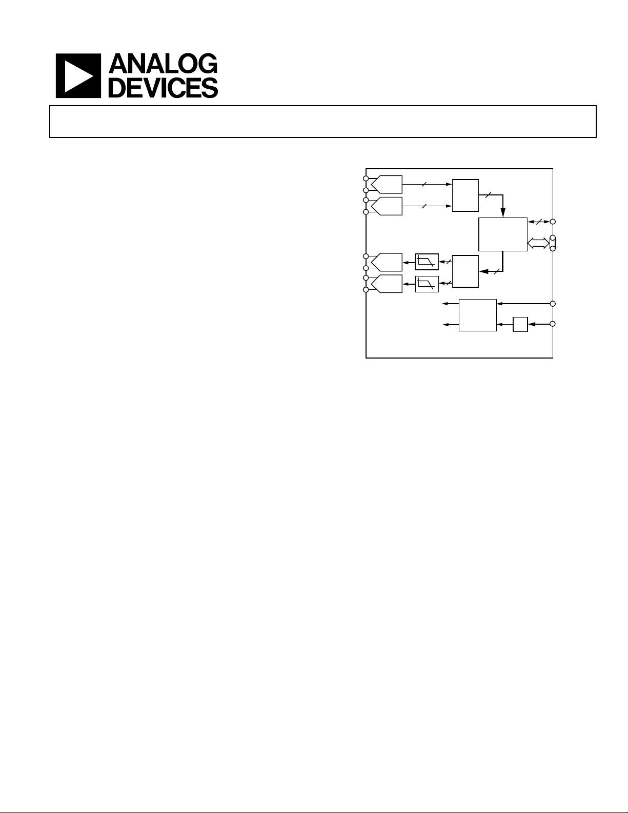
AD9863
FUNCTIONAL BLOCK DIAGRAM
VIN+A
VIN–A
VIN+B
VIN–B
IOUT+
IOUT–A
IOUT+B
IOUT–B
In half-duplex systems, the interface supports 24-bit parallel
transfers or 12-bit interleaved transfers. In full-duplex systems,
the interface supports an 12-bit interleaved ADC bus and an
12-bit interleaved TxDAC bus. The flexible I/O bus reduces pin
count and, therefore, reduces the required package size on the
AD9863 and the device to which it connects.
The AD9863 can use either mode pins or a serial programmable interface (SPI) to configure the interface bus, operate the
ADC in a low power mode, configure the TxDAC interpolation
rate, and control ADC and TxDAC power-down. The SPI
provides more programmable options for both the TxDAC path
(for example, coarse and fine gain control and offset control for
channel matching) and the ADC path (for example, the internal
duty cycle stabilizer, and twos complement data format).
The AD9863 is packaged in a 64-lead LFCSP (low profile, fine
pitched, chip scale package). The 64-lead LFCSP footprint is
only 9 mm × 9 mm, and is less than 0.9 mm high, fitting into
tightly spaced applications such as PCMCIA cards.
ADC
ADC
DAC
DAC
LOW-PASS
INTERPOLATION
FILTER
DAC CLOCK
AD9863
DATA
MUX
AND
LATCH
DATA
LATCH
AND
DEMUX
CLOCK
GENERATION
BLOCK
Figure 1.
Rx DATA
I/O
INTERFACE
CONFIGURATION
BLOCK
Tx DATA
PLL
I/O
INTERFACE
CONTROL
FLEXIBLE
I/O BUS
[0:23]
CLKIN1ADC CLOCK
CLKIN2
03604-0-070
Rev. 0
Information furnished by Analog Devices is believed to be accurate and reliable.
However, no responsibility is assumed by Analog Devices for its use, nor for any
infringements of patents or other rights of third parties that may result from its use.
Specifications subject to change without notice. No license is granted by implication
or otherwise under any patent or patent rights of Analog Devices. Trademarks and
registered trademarks are the property of their respective owners.
One Technology Way, P.O. Box 9106, Norwood, MA 02062-9106, U.S.A.
Tel: 781.329.4700
Fax: 781.326.8703 © 2003 Analog Devices, Inc. All rights reserved.
www.analog.com
Page 2

AD9863
TABLE OF CONTENTS
Tx Path Specifications...................................................................... 3
Theory of Operation...................................................................... 18
Rx Path Specifications...................................................................... 4
Power Specifications......................................................................... 5
Digital Specifications........................................................................ 5
Timing Specifications....................................................................... 6
Absolute Maximum Ratings............................................................ 7
ESD Caution.................................................................................. 7
Pin Configuration and Pin Function Descriptions...................... 8
Typical Performance Characteristics ........................................... 10
Te r m in o l o g y .................................................................................... 17
REVISION HISTORY
Revision 0: Initial Version
System Block ............................................................................... 18
Rx Path Block.............................................................................. 18
Tx Path Block.............................................................................. 20
Digital Block................................................................................ 23
Programmable Registers............................................................ 33
Clock Distribution Block .......................................................... 36
Outline Dimensions....................................................................... 40
Ordering Guide .......................................................................... 40
Rev. 0 | Page 2 of 40
Page 3
AD9863
Tx PATH SPECIFICATIONS
Table 1. F
AVDD = DVDD = 3.3 V, unless otherwise noted
Parameter Temp Test Level Min Typ Max Unit
Tx PATH GENERAL
Resolution Full IV 12 Bits
Maximum DAC Update Rate Full IV 200 MHz
Maximum Full-Scale Output Current Full IV 20 mA
Full-Scale Error Full V 1%
Gain Mismatch Error 25°C IV –3.5 +3.5 % FS
Offset Mismatch Error Full IV –0.1 +0.1 % FS
Reference Voltage Full V 1.23 V
Output Capacitance Full V 5 pF
Phase Noise (1 kHz Offset, 6 MHz Tone) 25°C V –115 dBc/Hz
Output Voltage Compliance Range Full IV –1.0 +1.0 V
TxPGA Gain Range Full V 20 dB
TxPGA Step Size Full V 0.10 dB
Tx PATH DYNAMIC PERFORMANCE
= 20 mA; F
(I
OUTFS
SNR Full IV 70.8 71.6 dB
SINAD Full IV 64.3 71 dB
THD Full IV −79 −66.3 dBc
SFDR, Wideband (DC to Nyquist) Full IV 68.5 77 dBc
SFDR, Narrowband (1 MHz Window) Full IV 72.8 81 dBc
1
See Figure 2 for description of the TxDAC termination scheme.
= 200 MSPS; 4× interpolation; R
DAC
= 1 MHz)
OUT
= 4.02 kΩ; differential load resistance of 100 Ω1; TxPGA = 20 dB,
SET
TxDAC
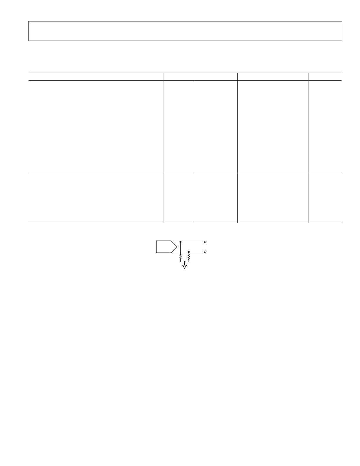
50Ω 50Ω
03604-0-071
Figure 2. Diagram showing Termination of100 Ω Differential
Load for Some TxDAC Measurements
Rev. 0 | Page 3 of 40
Page 4

AD9863
Rx PATH SPECIFICATIONS
Table 2. F
Parameter Temp Test Level Min Typ Max Unit
Rx PATH GENERAL
Resolution Full V 12 Bits
Maximum ADC Sample Rate Full IV 50 MSPS
Gain Mismatch Error Full V
Offset Mismatch Error Full V
Reference Voltage Full V 1.0 V
Reference Voltage (REFT–REFB) Error Full IV –30
Input Resistance (Differential) Full V 2 kΩ
Input Capacitance Full V 5 pF
Input Bandwidth Full V 30 MHz
Differential Analog Input Voltage Range Full V 2 V p-p differential
Rx PATH DC ACCURACY
Integral Nonlinearity (INL) 25°C V
Differential Nonlinearity (DNL) 25°C V
Aperature Delay 25°C V 2.0 ns
Aperature Uncertainty (Jitter) 25°C V 1.2 ps rms
Input Refered Noise 25°C V 250 uV
AD9863 Rx PATH DYNAMIC PERFORMANCE
(V
= –0.5 dBFS; FIN = 10 MHz)
IN
SNR Full V 67 dBc
SINAD Full V 65.5 dBc
THD (Second to Ninth Harmonics) Full IV −73 −66.6 dBc
SFDR, Wideband (DC to Nyquist) Full IV 68.3 74 dBc
Crosstalk between ADC Inputs Full V 80 dB
= 50 MSPS; internal reference; differential analog inputs, ADC_AVDD = DVDD = 3.3 V, unless otherwise noted
ADC
±0.2
±0.1
±6
±0.75
±0.75
% FS
% FS
+30 mV
LSB
LSB
Rev. 0 | Page 4 of 40
Page 5

AD9863
POWER SPECIFICATIONS
Table 3. Analog and digital supplies = 3.3 V; F
Parameter Temp Test Level Min Typ Max Unit
POWER SUPPLY RANGE
Analog Supply Voltage (AVDD) Full IV 2.7 3.6 V
Digital Supply Voltage (DVDD) Full IV 2.7 3.6 V
Driver Supply Voltage (DRVDD)
ANALOG SUPPLY CURRENTS
TxPath (20 mA Full-Scale Outputs) Full V 70 mA
TxPath (2 mA Full-Scale Outputs) Full V 20 mA
Rx Path (50 MSPS) Full V 103 mA
RxPath (50 MSPS, Low Power Mode) Full V 69 mA
RxPath (20 MSPS, Low Power Mode) Full V 55 mA
TxPath, Power-Down Mode Full V 2 mA
RxPath, Power-Down Mode Full V 5 mA
PLL Full V 12 mA
DIGITAL SUPPLY CURRENTS
TxPath, 1× Interpolation,
50 MSPS DAC Update for Both DACs,
Half-Duplex 24 Mode
TxPath, 2× Interpolation,
100 MSPS DAC Update for Both DACs,
Half-Duplex 24 Mode
TxPath, 4× Interpolation,
200 MSPS DAC Update for Both DACs,
Half-Duplex 24 Mode
RxPath Digital, Half-Duplex 24 Mode Full V 15 mA
CLKIN1
= F
= 50 MHz; PLL 4× setting; normal timing mode
CLKIN2
Full IV 2.7 3.6 V
Full V 20 mA
Full V 50 mA
Full V 80 mA
DIGITAL SPECIFICATIONS
Table 4.
Parameter Temp Test Level Min Typ Max Unit
LOGIC LEVELS
Input Logic High Voltage, V
Input Logic Low Voltage, V
Output Logic High Voltage, VOH (1 mA Load) Full IV DRVDD – 0.6 V
Output Logic Low Voltage, VOL (1 mA Load) Full IV 0.4 V
DIGITAL PIN
Input Leakage Current Full IV 12 µA
Input Capacitance Full IV 3 pF
Minimum RESET Low Pulse Width Full IV 5 Input Clock Cycles
Digital Output Rise/Fall Time Full IV 2.8 4 ns
IH
IL
Full IV DRVDD – 0.7 V
Full IV 0.4 V
Rev. 0 | Page 5 of 40
Page 6

AD9863
TIMING SPECIFICATIONS
Table 5.
Parameter Temp Test Level Min Typ Max Unit
INPUT CLOCK
CLKIN2 Clock Rate (PLL Bypassed) Full IV 1 200 MHz
PLL Input Frequency Full IV 16 200 MHz
PLL Ouput Frequency Full IV 32 350 MHz
TxPATH DATA
Setup Time
(HD24 Mode, Time Required before Data Latching Edge)
Hold Time
(HD24 Mode, Time Required after Data Latching Edge)
Latency 1× Interpolation (Data In until Peak Output Response) Full V 7 DAC Clock Cycles
Latency 2× Interpolation (Data In until Peak Output Response) Full V 35 DAC Clock Cycles
Latency 4× Interpolation (Data In until Peak Output Response) Full V 83 DAC Clock Cycles
RxPATH DATA
Output Delay (HD24 Mode, tOD) Full V –1.5
Latency Full V 5 ADC Clock Cycles
Full V 5
Full V –1.5
ns (see Clock
Distribution Block
section)
ns (see Clock
Distribution Block
section)
ns ( see Clock
Distribution Block
section)
Table 6. Explanation of Test Levels
Level Description
I 100% production tested.
II
III Sample tested only.
IV Parameter is guaranteed by design and characterization testing.
V Parameter is a typical value only.
VI
100% production tested at 25°C and guaranteed by design and characterization at specified temperatures.
100% production tested at 25°C and guaranteed by design and characterization for industrial temperature range.
Rev. 0 | Page 6 of 40
Page 7

AD9863
ABSOLUTE MAXIMUM RATINGS
Table 7.
Parameter Rating
Electrical
AVDD Voltage 3.9 V max
DRVDD Voltage 3.9 V max
Analog Input Voltage –0.3 V to AVDD + 0.3 V
Digital Input Voltage –0.3 V to DVDD – 0.3 V
Digital Output Current 5 mA max
Environmental
Operating Temperature Range
(Ambient)
Maximum Junction Temperature
Lead Temperature
(Soldering, 10 sec)
Storage Temperature Range
(Ambient)
–40°C to +85°C
150°C
300°C
–65°C to +150°C
Thermal Resistance
64-lead LFCSP (4-layer board):
θ
= 24.2 (paddle soldered to ground plan, 0 LPM air)
JA
= 30.8 (paddle not soldered to ground plan, 0 LPM air)
θ
JA
Stresses above those listed under the Absolute Maximum
Ratings may cause permanent damage to the device. This is a
stress rating only; functional operation of the device at these or
any other conditions above those indicated in the operational
section of this specification is not implied. Exposure to absolute
maximum rating conditions for extended periods may affect
device reliability.
ESD CAUTION
ESD (electrostatic discharge) sensitive device. Electrostatic charges as high as 4000 V readily accumulate on the
human body and test equipment and can discharge without detection. Although this product features
proprietary ESD protection circuitry, permanent damage may occur on devices subjected to high energy
electrostatic discharges. Therefore, proper ESD precautions are recommended to avoid performance
degradation or loss of functionality.
Rev. 0 | Page 7 of 40
Page 8
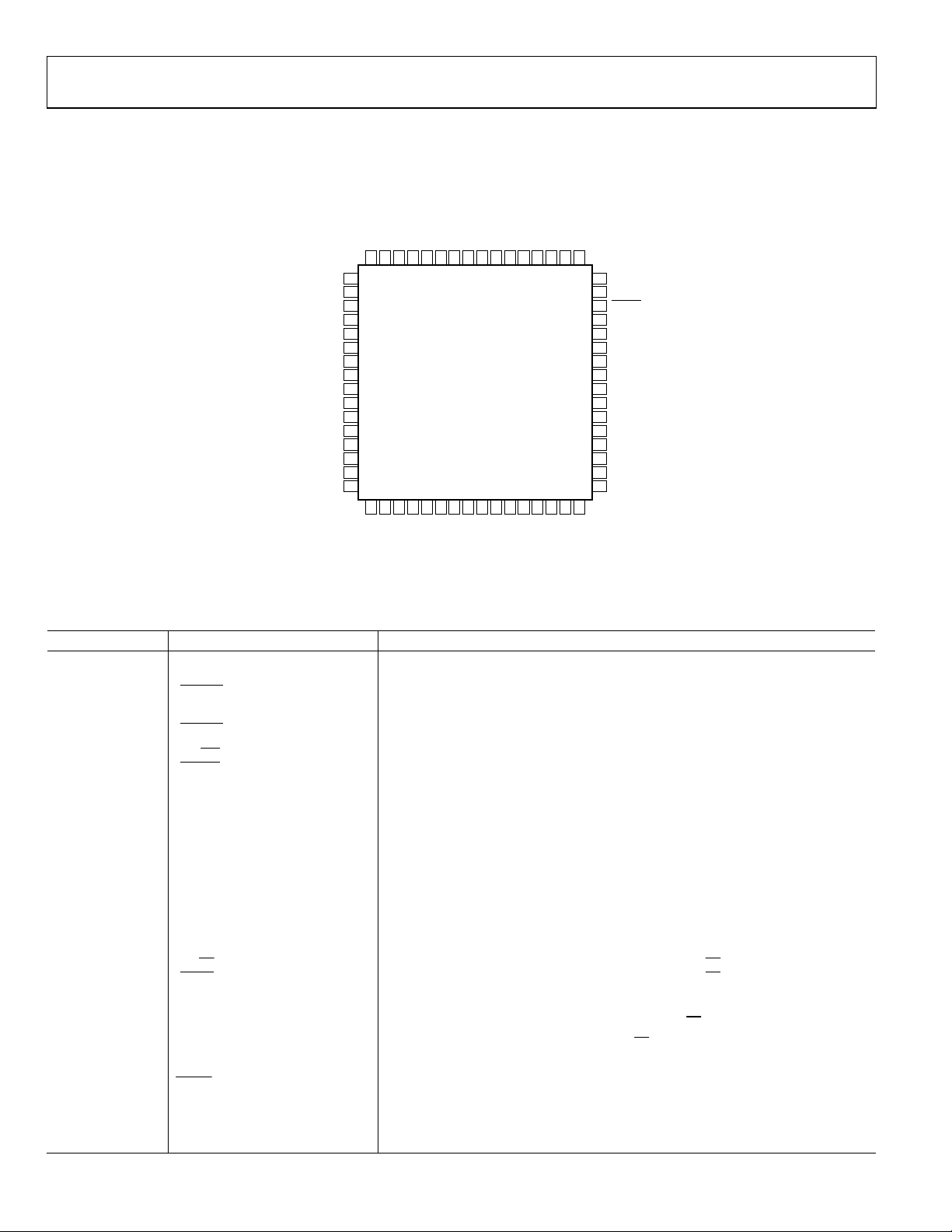
AD9863
A
R
PIN CONFIGURATION AND PIN FUNCTION DESCRIPTIONS
SPI_DIO
SPI_CLK
SPI_SDO
DC_LO_PW
DVDD
DVSS
AVDD
IOUT–A
IOUT+A
AGND
REFIO
FSADJ
AGND
IOUT+B
IOUT–B
AVDD
SPI_CS64TxPWRDWN63RxPWRDWN62ADC_AVDD61REFT60ADC_AVSS59VIN+A58VIN–A57VREF56VIN–B55VIN+B54ADC_AVSS53REFB52ADC_AVDD51PLL_AVDD50PLL_AVSS
1
2
3
4
5
6
7
8
9
10
11
12
13
14
15
16
18
19
U11
IFACE217IFACE3
AD9863
TOP VIEW
(Not to Scale)
20U921U822U723U624U525U426U327U228U129U030
U10
49
48
CLKIN1
CLKIN2
47
46
RESET
L0
45
L1
44
43
L2
L3
42
L4
41
40
L5
L6
39
38
L7
L8
37
L9
36
35
L10
L11
34
IFACE1
33
31
32
DRVDD
DRVSS
03604-0-072
Figure 3. Pin Configuration
Table 8. Pin Function Descriptions
Pin No. Name
1
1 SPI_DIO
(
Interp1)
2 SPI_CLK
(
Interp0)
3 SPI_SDO
FD/HD)
(
Description
SPI: Serial Port Data Input.
No SPI: Tx Interpolation Pin, MSB.
SPI: Serial Port Shift Clock.
No SPI: Tx Interpolation Pin, LSB.
SPI: 4-Wire Serial Port Data Output
No SPI: Configures Full-Duplex or Half-Duplex Mode.
2, 3
4 ADC_LO_PWR ADC Low Power Mode Enable. Defined at power-up.
5, 31 DVDD, DRVDD Digital Supply.
6, 32 DVSS, DRVDD Digital Ground.
7, 16, 50, 51, 61 AVDD Analog Supply.
8, 9 IOUT-A, IOUT+A DAC A Differential Output.
10, 13, 49, 53, 59 AGND, AVSS Analog Ground.
11 REFIO Tx DAC Band Gap Reference Decoupling Pin.
12 FSADJ Tx DAC Full-Scale Adjust Pin.
14, 15 IOUT+B, IOUT−B DAC B Differential Output.
17 IFACE2
(12/24)
SPI: Buffered CLKIN. Can be configured as system clock output.
No SPI: For FD: Buffered CLKIN; For HD24 or HD12: 12/
18 IFACE3 Clock Output.
19–30 U11–U0 Upper Data Bit 11 to Upper Data Bit 0.
33 IFACE1
SPI: For FD: TxSYNC; For HD24, HD12, or Clone: Tx/Rx.
No SPI: FD >> TxSYNC; HD24 or HD12: Tx/Rx.
34–45 L11–L0 Lower Data Bit 11 to Lower Data Bit 0.
46
RESET
Chip Reset When Low.
47 CLKIN2 Clock Input 2.
48 CLKIN1 Clock Input 1
52 REFB ADC Bottom Reference.
Rev. 0 | Page 8 of 40
24 Configuration Pin.
Page 9

AD9863
Pin No. Name
1
Description
2, 3
54, 55 VIN+B, VIN−B ADC B Differential Input.
56 VREF ADC Band Gap Reference.
57, 58 VIN−A, VIN+A ADC A Differential Input.
60 REFT ADC Top Reference.
62 RxPwrDwn Rx Analog Power-Down Control.
63 TxPwrDwn Tx Analog Power-Down Control.
64 SPI_CS
1
Underlined pin names and descriptions apply when the device is configured without a serial port interface, referred to as No SPI mode.
2
Some pin descriptions depend if a serial port is used (SPI mode) or not (No SPI mode), indicated by the labels SPI and No SPI.
3
Some pin descriptions depend on the interface configuration: full-duplex (FD), half-duplex interleaved data (HD12), half-duplex parallel data (HD24), and a half-duplex
interface similar to the AD9860 and AD9862 data interface called clone mode (Clone). Clone mode requires a serial port interface.
SPI: Serial Port Chip Select. At power-up or reset, this must be high.
No SPI: Tie low to disable SPI and use mode pins. This pin must be tied low.
Rev. 0 | Page 9 of 40
Page 10
AD9863
TYPICAL PERFORMANCE CHARACTERISTICS
0
–10
–20
–30
40
–50
–60
–70
AMPLITUDE (dBFS)
–80
–90
–100
–110
0 5 10 15 20 25
FREQUENCY (MHz)
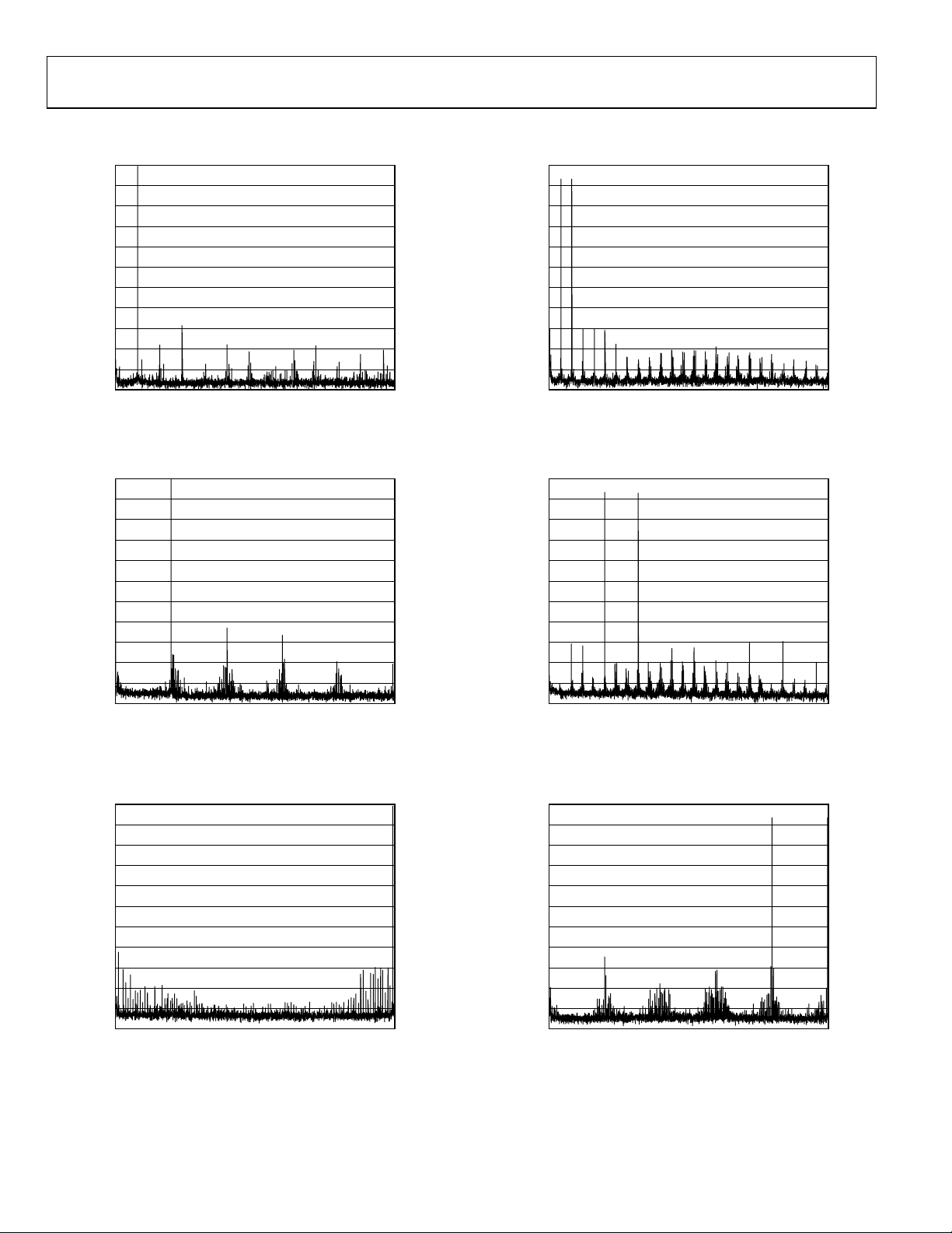
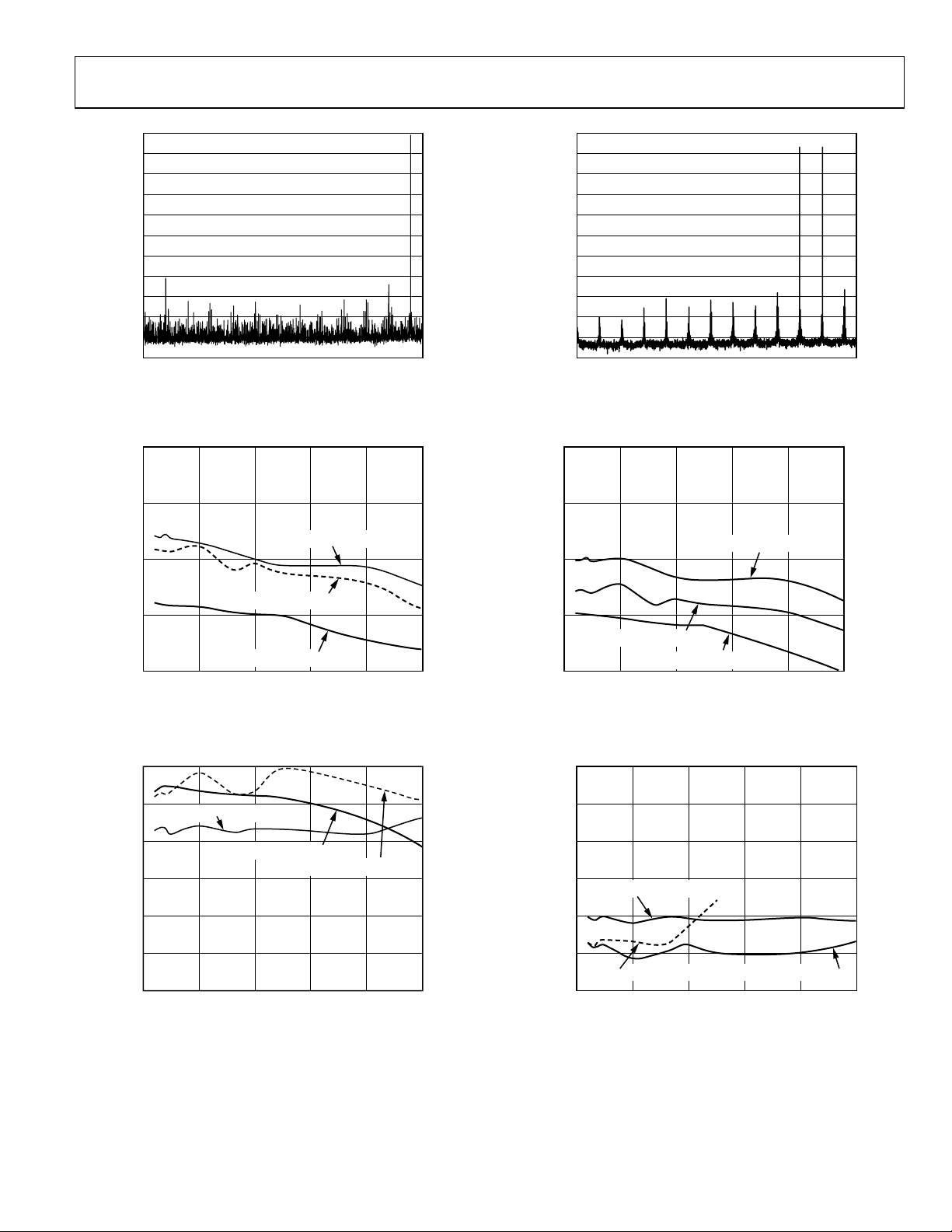
Figure 4. AD9863 Rx Path Single-Tone FFT of Rx Channel B Path
Digitizing 2 MHz Tone
03604-0-001
0
–10
–20
–30
40
–50
–60
–70
AMPLITUDE (dBFS)
–80
–90
–100
–110
0 5 10 15 20 25
FREQUENCY (MHz)
Figure 7. AD9863 Rx Path Dual-Tone FFT of Rx Channel A Path
Digitizing 1 MHz and 2 MHz Tones
03604-0-004
0
–10
–20
–30
40
–50
–60
–70
AMPLITUDE (dBFS)
–80
–90
–100
–110
0 5 10 15 20 25
FREQUENCY (MHz)
Figure 5. AD9863 Rx Path Single-Tone FFT of Rx Channel B Path
Digitizing 5 MHz Tone
0
–10
–20
–30
40
–50
–60
–70
AMPLITUDE (dBFS)
–80
–90
–100
–110
0 5 10 15 20 25
FREQUENCY (MHz)
Figure 6. AD9863 Rx Path Single-Tone FFT of Rx Channel B Path
Digitizing 24 MHz Tone
03604-0-002
03604-0-003
0
–10
–20
–30
40
–50
–60
–70
AMPLITUDE (dBFS)
–80
–90
–100
–110
0 5 10 15 20 25
FREQUENCY (MHz)
Figure 8. AD9863 Rx Path Dual-Tone FFT of Rx Channel A Path
Digitizing 5 MHz and 8 MHz Tones
0
–10
–20
–30
40
–50
–60
–70
AMPLITUDE (dBFS)
–80
–90
–100
–110
0 5 10 15 20 25
FREQUENCY (MHz)
Figure 9. AD9863 Rx Path Dual-Tone FFT of Rx Channel A Path
Digitizing 20 MHz and 25 MHz Tones
03604-0-005
03604-0-006
Rev. 0 | Page 10 of 40
Page 11
AD9863
0
–10
–20
–30
40
–50
–60
–70
AMPLITUDE (dBFS)
–80
–90
–100
–110
0 5 10 15 20 25
FREQUENCY (MHz)
Figure 10. AD9863 Rx Path Single-Tone FFT of Rx Channel B Path
Digitizing 76 MHz Tone
03604-0-007
0
–10
–20
–30
40
–50
–60
–70
AMPLITUDE (dBFS)
–80
–90
–100
–110
0 5 10 15 20 25
FREQUENCY (MHz)
Figure 13. AD9863 Rx Path Dual-Tone FFT of Rx Channel A Path
Digitizing 70 MHz and 72 MHz Tones
03604-0-010
74
71
LOW POWER @ 25MSPS
68
SNR (dBc)
65
62
0 5 10 15 20 25
NORMAL POWER @ 50MSPS
ULTRALOW POWER @ 16MSPS
INPUT FREQUENCY (MHz)
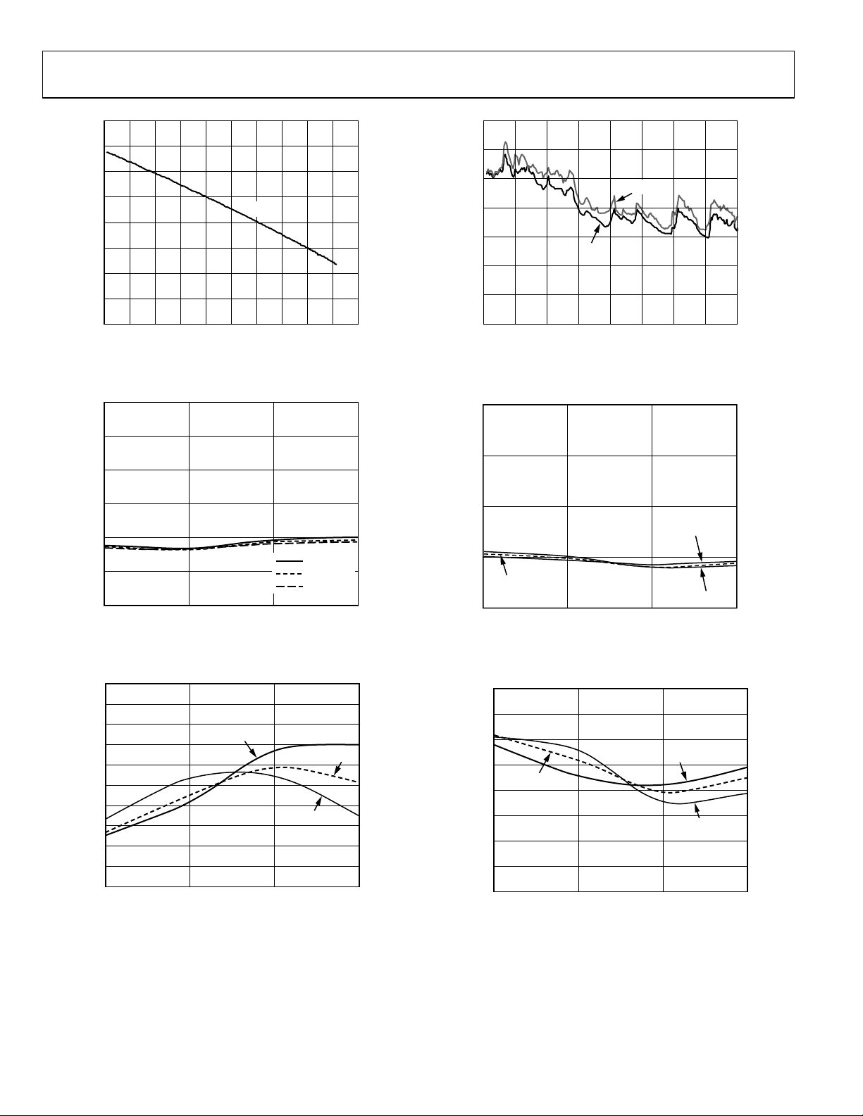
Figure 11. AD9863 Rx Path at 50 MSPS, 10 MHz Input Tone
SNR Performance vs. Input Frequency
80
75
NORMAL POWER @ 50MSPS
70
65
SFDR (dBc)
60
ULTRALOW POWER @ 16MSPS
LOW POWER @ 25MSPS
03604-0-008
74
71
68
SINAD (dBc)
65
NORMAL POWER @ 50MSPS
62
0 5 10 15 20 25
ULTRALOW POWER @ 16MSPS
INPUT FREQUENCY (MHz)
LOW POWER @ 25MSPS
Figure 14. AD9863 Rx Path at 50 MSPS, 10 MHz Input Tone
SINAD Performance vs. Input Frequency
–50
–55
–60
–65
NORMAL POWER @ 50MSPS
THD (dBc)
–70
12.0
11.8
11.6
11.4
11.2
11.0
10.8
10.6
10.4
10.2
10.0
ENOB (Bits)
03604-0-011
55
50
0 5 10 15 20 25
INPUT FREQUENCY (MHz)
Figure 12. AD9863 Rx Path at 50 MSPS, 10 MHz Input Tone
SFDR Performance vs. Input Frequency
03604-0-009
Rev. 0 | Page 11 of 40
–75
ULTRALOW POWER @ 16MSPS
–80
0 5 10 15 20 25
INPUT FREQUENCY (MHz)
LOW POWER @ 25MSPS
Figure 15. AD9863 Rx Path at 50 MSPS, 10 MHz Input Tone
THD Performance vs. Input Frequency
03604-0-012
Page 12
AD9863
80
90
–90
70
60
50
40
SNR (dBc)
30
20
10
0
0 –5 –10 –15 –20 –25 –30 –35 –40 –45 –50
INPUT AMPLITUDE (dBFS)
SNR
Figure 16. AD9863 Rx Path at 50 MSPS, 10 MHz Input Tone
SNR Performance vs. Input Amplitude
74
72
70
68
SNR (dBc)
66
64
62
3.6 3.3 3.0 2.7
INPUT AMPLITUDE (dBFS)
AVE –40°C
AVE +25°C
AVE +85°C
Figure 17. AD9863 Rx Path at 50 MSPS, 10 MHz Input Tone
SNR Performance vs. ADC_AVDD and Temperature
–70.0
–70.5
–71.0
–71.5
–72.0
–72.5
THD (dBc)
–73.0
–73.5
–74.0
–74.5
–75.0
2.7 3.0 3.3 3.6
INPUT AMPLITUDE (dBFS)
AVE –40°C
AVE +25°C
AVE +85°C
Figure 18. AD9863 Rx Path Single-Tone THD Performance vs.
ADC_AVDD and Temperature
03604-0-013
03604-0-014
03604-0-015
80
70
60
50
SFDR (dBFS)
40
30
20
0 –5 –10 –15 –20 –25 –30 –35 –40
THD
INPUT AMPLITUDE (dBFS)
SFDR
Figure 19. AD9863 Rx Path at 50 MSPS, 10 MHz Input Tone
THD and SFDR Performance vs. Input Amplitude
74
71
68
SINAD (dBc)
65
AVE +25°C
62
2.7 3.0 3.3 3.6
INPUT FREQUENCY (MHz)
AVE +85°C
AVE –40°C
Figure 20. AD9863 Rx Path at 50 MSPS, 10 MHz Input Tone
SINAD Performance vs. ADC_AVDD and Temperature
78
77
76
75
AVE +25°C
74
SFDR (dBc)
73
72
71
70
2.7 3.0 3.3 3.6
INPUT AMPLITUDE (dBFS)
AVE +85°C
AVE –40°C
Figure 21. AD9863 Rx Path Single-Tone SFDR Performance vs.
ADC_AVDD and Temperature
–80
–70
–60
–50
–40
–30
–20
12.0
11.8
11.6
11.4
11.2
11.0
10.8
10.6
10.4
10.2
10.0
THD (dBFS)
03604-0-016
ENOB (Bits)
03604-0-017
03604-0-018
Rev. 0 | Page 12 of 40
Page 13

AD9863
0
–10
–20
–30
40
–50
–60
–70
AMPLITUDE (dBc)
–80
–90
–100
–110
0 5 10 15 20 25
FREQUENCY (MHz)
Figure 22. AD9863 Tx Path 1 MHz Single-Tone Output FFT of Tx Path
with 20 mA Full-Scale Output into 33 Ω Differential Load
03604-0-019
0
–10
–20
–30
40
–50
–60
–70
AMPLITUDE (dBc)
–80
–90
–100
–110
0 5 10 15 20 25
FREQUENCY (MHz)
03604-0-022
Figure 25. AD9863 Tx Path 5 MHz Single-Tone Output FFT of Tx Channel A
with 20 mA Full-Scale Output into 33 Ω Differential Load
–50
–60
–70
THD
THD (dBc)
–80
SFDR
–90
–100
0 5 10 15 20 25
OUTPUT FREQUENCY (MHz)
50
60
70
80
90
100
SFDR (dBc)
03604-0-020
Figure 23. AD9863 Tx Path THD/SFDR vs. Output Frequency of Tx Channel A,
with 20 mA Full-Scale Output into 60 Ω Differential Load
–50
–60
–70
THD (dBc)
–80
–90
–100
2mA, 600Ω
0 5 10 15 20 25
OUTPUT FREQUENCY (MHz)
20mA, 60Ω
20mA, 33Ω
03604-0-021
Figure 24. AD9863 Tx Path THD vs. Output Frequency of Tx Channel A
74
72
SNR
70
68
SNR/SINAD (dBc)
66
64
62
0 5 10 15 20
SINAD
OUTPUT FREQUENCY (MHz)
03604-0-023
25
Figure 26. AD9863 Tx Path SINAD/SNR vs. Output Frequency of Tx Path
with 20 mA Full-Scale Output into 60 Ω Differential Load
–50
–55
–60
–65
–70
–75
IMD (dBc)
–80
–85
–90
–95
–100
0 5 10 15 20 25
OUTPUT FREQUENCY (MHz)
20mA, 60Ω
2mA, 600Ω
20mA, 33Ω
03604-0-024
Figure 27. AD9863 Tx Path Dual-Tone (0.5 MHz Spacing) IMD vs.
Output Frequency
Rev. 0 | Page 13 of 40
Page 14

AD9863
Figure 28 to Figure 33 use the same input data to the Tx path, a 64-carrier OFDM signal over a 20 MHz bandwidth, centered at 20 MHz.
The center two carriers are removed from the signal to observe the in-band intermodulation distortion (IMD) from the DAC output.
–20
–30
–40
–50
–60
–70
–80
AMPLITUDE (dBc)
–90
–100
–110
–120
7.5 12.5 17.5 22.5 27.5 32.5
FREQUENCY (MHz)
03604-0-025
Figure 28. AD9863 Tx Path FFT, 64-Carrier (Center Two Carriers Removed)
OFDM Signal over 20 MHz Bandwidth, Centered at 20 MHz, with
20 mA Full-Scale Output into 60 Ω Differential Load
–20
–30
–40
–50
–60
–70
–80
AMPLITUDE (dBc)
–90
–100
–110
–120
7.5 8.0 8.5 9.0 9.5 10.0 10.5 11.0 11.5 12.0 12.5
FREQUENCY (MHz)
03604-0-026
Figure 29. AD9863 Tx Path FFT, Lower Band IMD Products of
OFDM Signal in Figure 28
–20
–30
–40
–50
–60
–70
–80
AMPLITUDE (dBc)
–90
–100
–110
–120
0 1020304050607080
FREQUENCY (MHz)
03604-0-027
Figure 30. AD9863 Tx Path FFT of OFDM Signal in Figure 28 with
1x Interpolation
–20
–30
–40
–50
–60
–70
–80
AMPLITUDE (dBc)
–90
–100
–110
–120
18.75 19.25 19.75 20.25 20.75 21.25
FREQUENCY (MHz)
Figure 31. AD9863 Tx Path FFT, In-Band IMD Products of
OFDM Signal in Figure 28
–20
–30
–40
–50
–60
–70
–80
AMPLITUDE (dBc)
–90
–100
–110
–120
27.5 28.0 28.5 29.0 29.5 30.0 30.5 31.0 31.5 32.0 32.5
FREQUENCY (MHz)
Figure 32. AD9863 Tx Path FFT, Lower Band IMD Products of
OFDM Signal in Figure 28
–20
–30
–40
–50
–60
–70
–80
AMPLITUDE (dBc)
–90
–100
–110
–120
0 1020304050607080
FREQUENCY (MHz)
Figure 33. AD9863 Tx Path FFT of OFDM Signal in
Figure 28 with 2x Interpolation
03604-0-028
03604-0-029
03604-0-030
Rev. 0 | Page 14 of 40
Page 15

AD9863
Figure 34 to Figure 39 use the same input data to the Tx path, a 256-carrier OFDM signal over a 1.75 MHz bandwidth, centered at 7 MHz.
The center four carriers are removed from the signal to observe the in-band intermodulation distortion (IMD) from the DAC output.
–30
–40
–50
–60
–70
–80
–90
AMPLITUDE (dBc)
–100
–110
–120
–130
6.0 6.2 6.4 6.6 6.8 7.0 7.2 7.4 7.6 7.8 8.0
FREQUENCY (MHz)
Figure 34. AD9863 Tx Path FFT, 256-Carrier (Center Four Carriers Removed)
OFDM Signal over 1.75 MHz Bandwidth, Centered at 7 MHz, with
20 mA Full-Scale Output into 60 Ω Differential Load
–30
–40
–50
–60
–70
–80
–90
AMPLITUDE (dBc)
–100
–110
–120
–130
6.06 6.08 6.10 6.12 6.14 6.16 6.18
FREQUENCY (MHz)
Figure 35. AD9863 Tx Path FFT, Lower-Band IMD Products of
OFDM Signal in Figure 34
–30
–40
–50
–60
–70
–80
–90
AMPLITUDE (dBc)
–100
–110
–120
–130
0 5 10 15 20 25
FREQUENCY (MHz)
Figure 36. AD9863 Tx Path FFT of OFDM Signal in Figure 34,
with 1× Interpolation
03604-0-031
03604-0-032
03604-0-033
Rev. 0 | Page 15 of 40
–30
–40
–50
–60
–70
–80
–90
AMPLITUDE (dBc)
–100
–110
–120
–130
6.97 6.98 6.99 7.00 7.01 7.02 7.03
FREQUENCY (MHz)
Figure 37. AD9863 Tx Path FFT, In-Band IMD Products of
OFDM Signal in Figure 34
–30
–40
–50
–60
–70
–80
–90
AMPLITUDE (dBc)
–100
–110
–120
–130
7.81 7.83 7.85 7.87 7.89 7.91 7.93
FREQUENCY (MHz)
Figure 38. AD9863 Tx Path FFT, Upper-Band IMD Products of
OFDM Signal in Figure 34
–30
–40
–50
–60
–70
–80
–90
AMPLITUDE (dBc)
–100
–110
–120
–130
0 5 10 15 20 25
FREQUENCY (MHz)
Figure 39. AD9863 Tx Path FFT of OFDM Signal in Figure 34,
with 2× Interpolation
03604-0-034
03604-0-035
03604-0-036
Page 16

AD9863
Figure 40 to Figure 45 use the same input data to the Tx path, a 256-carrier OFDM signal over a 23 MHz bandwidth, centered at 23 MHz.
The center four carriers are removed from the signal to observe the in-band intermodulation distortion (IMD) from the DAC output.
–30
–40
–50
–60
–70
–80
–90
AMPLITUDE (dBc)
–100
–110
–120
9 141924 3429
FREQUENCY (MHz)
03604-0-037
Figure 40. AD9863 Tx Path FFT, 256-Carrier (Center Four Carriers Removed)
OFDM Signal over 23 MHz Bandwidth, Centered at 7 MHz, with
20 mA Full-Scale Output into 60 Ω Differential Load
–30
–40
–50
–60
–70
–80
–90
AMPLITUDE (dBc)
–100
–110
–120
10.5 10.7 10.9 11.1 11.3 11.5 11.7 11.9 12.1 12.3 12.5
FREQUENCY (MHz)
03604-0-038
Figure 41. AD9863 Tx Path FFT, Lower-Band IMD Products of
OFDM Signal in Figure 40
–30
–40
–50
–60
–70
–80
–90
AMPLITUDE (dBc)
–100
–110
–120
0 102030405060708090
FREQUENCY (MHz)
03604-0-039
Figure 42. AD9863 Tx Path FFT of OFDM Signal in Figure 40,
with 1× Interpolation
Rev. 0 | Page 16 of 40
–30
–40
–50
–60
–70
–80
–90
AMPLITUDE (dBc)
–100
–110
–120
6.97 6.98 6.99 7.00 7.01 7.02 7.03
FREQUENCY (MHz)
03604-0-040
Figure 43. AD9863 Tx Path FFT, In-Band IMD Products of
OFDM Signal in Figure 40
–30
–40
–50
–60
–70
–80
–90
AMPLITUDE (dBc)
–100
–110
–120
33.5 33.7 33.9 34.1 34.3 34.5 34.7 34.9 35.1 35.3 35.5
FREQUENCY (MHz)
03604-0-041
Figure 44. AD9863 Tx Path FFT, Upper-Band IMD Products of
OFDM Signal in Figure 40
–30
–40
–50
–60
–70
–80
–90
AMPLITUDE (dBc)
–100
–110
–120
0 102030405060708090
FREQUENCY (MHz)
03604-0-042
Figure 45. AD9863 Tx Path FFT of OFDM Signal in Figure 40,
with 2× Interpolation
Page 17

AD9863
TERMINOLOGY
Input Bandwidth
The analog input frequency at which the spectral power of the
fundamental frequency (as determined by the FFT analysis) is
reduced by 3 dB.
Aperture Delay
The delay between the 50% point of the rising edge of the
CLKIN1 signal and the instant at which the analog input is
actually sampled.
Aperture Uncertainty (Jitter)
The sample-to-sample variation in aperture delay.
Harmonic Distortion, Second
The ratio of the rms signal amplitude to the rms value of the
second harmonic component, reported in dBc.
Harmonic Distortion, Third
The ratio of the rms signal amplitude to the rms value of the
third harmonic component, reported in dBc.
Integral Nonlinearity
The deviation of the transfer function from a reference line
measured in fractions of an LSB using a “best straight line”
determined by a least square curve fit.
Crosstalk
Coupling onto one channel being driven by a –0.5 dBFS signal
when the adjacent interfering channel is driven by a full-scale
signal.
Differential Analog Input Voltage Range
The peak-to-peak differential voltage that must be applied to
the converter to generate a full-scale response. Peak differential
voltage is computed by observing the voltage on a single pin
and subtracting the voltage from the other pin, which is 180°
out of phase. Peak-to-peak differential is computed by rotating
the input phase 180° and taking the peak measurement again.
Then the difference is computed between both peak
measurements.
Differential Nonlinearity
The deviation of any code width from an ideal 1 LSB step.
Effective Number of Bits (ENOB)
The effective number of bits is calculated from the measured
SNR based on the following equation:
76.1 dBSNR
ENOB
=
MEASURED
−
02.6
Pulse Width/Duty Cycle
Pulse width high is the minimum amount of time that a signal
should be left in the logic high state to achieve rated performance; pulse width low is the minimum time a signal should be
left in the low state, logic low.
Full-Scale Input Power
Expressed in dBm, full-scale input power is computed using the
following equation:
2
⎛
⎜
Power
FULLSCALE
log10
=
⎜
⎝
ZV
−
RMSFULLSCALE
001.0
INPUT
⎞
⎟
⎟
⎠
Gain Error
Gain error is the difference between the measured and ideal
full-scale input voltage range of the ADC.
Minimum Conversion Rate
The encode rate at which the SNR of the lowest analog signal
frequency drops by no more than 3 dB below the guaranteed
limit.
Maximum Conversion Rate
The encode rate at which parametric testing is performed.
Output Propagation Delay
The delay between a differential crossing of CLK+ and CLK−
and the time when all output data bits are within valid logic
levels.
Power Supply Rejection Ratio
The ratio of a change in input offset voltage to a change in
power supply voltage.
Signal-to-Noise and Distortion (SINAD)
The ratio of the rms signal amplitude (set 1 dB below full-scale)
to the rms value of the sum of all other spectral components,
including harmonics, but excluding dc.
Signal-to-Noise Ratio (without Harmonics)
The ratio of the rms signal amplitude (set at 1 dB below full
scale) to the rms value of the sum of all other spectral
components, excluding the first five harmonics and dc.
Spurious-Free Dynamic Range (SFDR)
The ratio of the rms signal amplitude to the rms value of the
peak spurious spectral component. The peak spurious
component may or may not be a harmonic. It also may be
reported in dBc (i.e., degrades as signal level is lowered) or
dBFS (i.e., always related back to converter full scale). SFDR
does not include harmonic distortion components.
Worst Oth e r S p u r
The ratio of the rms signal amplitude to the rms value of the
worst spurious component (excluding the second and third
harmonics) reported in dBc.
Rev. 0 | Page 17 of 40
Page 18

AD9863
V
V
THEORY OF OPERATION
SYSTEM BLOCK
The AD9863 is targeted to cover the mixed-signal front end
needs of multiple wireless communication systems. It features a
receive path that consists of dual 12-bit receive ADCs, and a
transmit path that consists of dual 12-bit transmit DACs
(TxDAC). The AD9863 integrates additional functionality
typically required in most systems, such as power scalability, Tx
gain control, and clock multiplication circuitry.
The AD9863 minimizes both size and power consumption to
address the needs of a range of applications from the low power
portable market to the high performance base station market.
The part is provided in a 64-lead lead frame chip scale package
(LFCSP) that has a footprint of only 9 mm × 9 mm. Power
consumption can be optimized to suit the particular application
beyond just a speed grade option by incorporating power-down
controls, low power ADC modes, TxDAC power scaling, and a
half-duplex mode, which automatically disables the unused
digital path.
The AD9863 uses two 12-bit buses to transfer Rx path data and
Tx path data. These two buses support 24-bit parallel data
transfers or 12-bit interleaved data transfers. The bus is
configurable through either external mode pins or through
internal registers settings. The registers allow many more
options for configuring the entire device.
The following sections discuss the various blocks of the AD9863:
Rx block, Tx block, the digital block, programmable registers
and the clock distribution block.
Rx PATH BLOCK
Rx Path General Description
The AD9863 Rx path consists of two 12-bit, 50 MSPS analog-todigital converters (ADCs). The dual ADC paths share the same
clocking and reference circuitry to provide optimal matching
characteristics. Each of the ADCs consists of a 9-stage differential pipelined switched capacitor architecture with output error
correction logic.
The pipelined architecture permits the first stage to operate on a
new input sample, while the remaining stages operate on
preceding samples. Sampling occurs on the falling edge of the
input clock. Each stage of the pipeline, excluding the last,
consists of a low resolution flash ADC and a residual multiplier
to drive the next stage of the pipeline. The residual multiplier
uses the flash ADC output to control a switched capacitor
digital-to-analog converter (DAC) of the same resolution. The
DAC output is subtracted from the stage’s input signal, and the
residual is amplified (multiplied) to drive the next pipeline
stage. The residual multiplier stage is also called a multiplying
DAC (MDAC). One bit of redundancy is used in each one of
the stages to facilitate digital correction of flash errors. The last
stage simply consists of a flash ADC.
The differential input stage is dc self-biased and allows
differential or single-ended inputs. The output-staging block
aligns the data, carries out the error correction, and passes the
data to the output buffers.
The latency of the Rx path is about 5 clock cycles.
Rx Path Analog Input Equivalent Circuit
The Rx path analog inputs of the AD9863 incorporate a novel
structure that merges the function of the input sample-andhold amplifiers (SHAs) and the first pipeline residue amplifiers
into a single, compact switched capacitor circuit. This structure
achieves considerable noise and power savings over a conventional implementation that uses separate amplifiers, by eliminating
one amplifier in the pipeline.
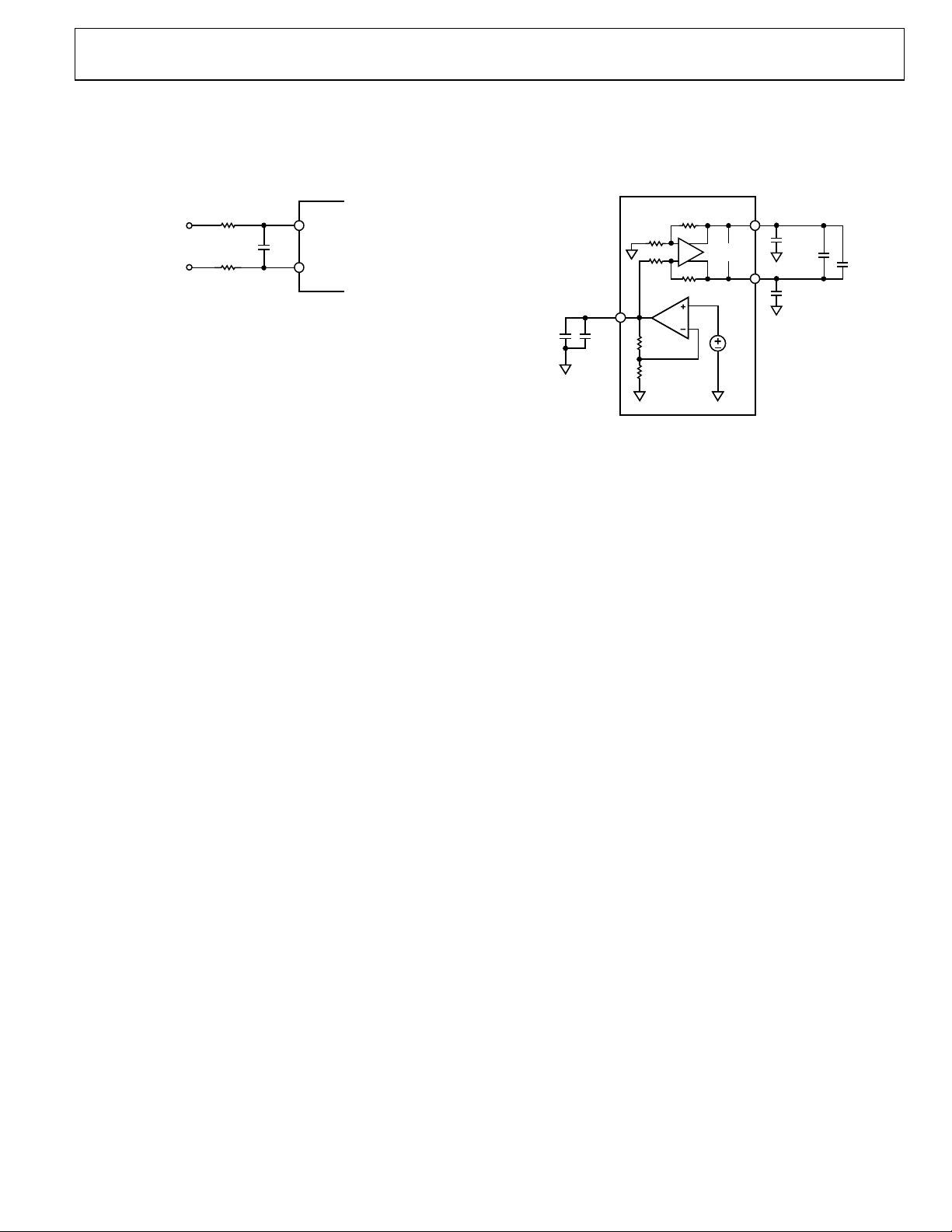
Figure 46 illustrates the equivalent analog inputs of the AD9863
(a switched capacitor input). Bringing CLK to logic high opens
switch S3 and closes switches S1 and S2; this is the sample mode
of the input circuit. The input source connected to VIN+ and
VIN− must charge capacitor C
during this time. Bringing CLK
H
to a logic low opens S2, and then switch S1 opens followed by
closing S3. This puts the input circuit into hold mode.
S1
C
IN+
IN–
R
IN
R
IN
Figure 46. Differential Input Architecture
C
V
IN
CM
C
IN
H
S3 S2
C
H
+
–
03604-0-073
The structure of the input SHA places certain requirements on
the input drive source. The differential input resistors are
typically 2 kΩ each. The combination of the pin capacitance,
C
, and the hold capacitance, CH, is typically less than 5 pF. The
IN
input source must be able to charge or discharge this capacitance to 12-bit accuracy in one-half of a clock cycle. When the
SHA goes into sample mode, the input source must charge or
discharge capacitor C
from the voltage already stored on it to
H
the new voltage. In the worst case, a full-scale voltage step on
the input source must provide the charging current through the
R
of switch S1 (typically 100 Ω) to a settled voltage within
ON
one-half of the ADC sample period. This situation corresponds
to driving a low input impedance. On the other hand, when the
source voltage equals the value previously stored on C
, the
H
hold capacitor requires no input current and the equivalent
input impedance is extremely high.
Rev. 0 | Page 18 of 40
Page 19
AD9863
Rx Path Application Section
Adding series resistance between the output of the signal source
and the VIN pins reduces the drive requirements placed on the
signal source. Figure 47 shows this configuration.
AD9863
R
SERIES
C
SHUNT
R
SERIES
Figure 47. Typical Input
VIN+
VIN–
03604-0-074
default 1 V VREF reference accepts a 2 V p-p differential input
swing and the offset voltage should be
REFT = AVDD/2 + 0.5 V
REFB = AVDD/2 – 0.5 V
AD9863
TO ADCs
VREF
REFT
REFB
0.1µF
0.1µF
0.1µF
10µF
The bandwidth of the particular application limits the size of
this resistor. For applications with signal bandwidths less than
10 MHz, the user may insert series input resistors and a shunt
capacitor to produce a low-pass filter for the input signal.
Additionally, adding a shunt capacitance between the VIN pins
can lower the ac load impedance. The value of this capacitance
depends on the source resistance and the required signal
bandwidth.
The Rx input pins are self-biased to provide this midsupply,
common-mode bias voltage, so it is recommended to ac couple
the signal to the inputs using dc blocking capacitors. In systems
that must use dc coupling, use an op amp to comply with the
input requirements of the AD9863. The inputs accept a signal
with a 2 V p-p differential input swing centered about one-half
of the supply voltage (AVDD/2). If the dc bias is supplied externally, the internal input bias circuit should be powered down by
writing to registers Rx_A dc bias [Register 0x3, Bit 6] and Rx_B
dc bias [Register 0x4, Bit 7].
The ADCs in the AD9863 are designed to sample differential
input signals. The differential input provides improved noise
immunity and better THD and SFDR performance for the Rx
path. In systems that use single-ended signals, these inputs can
be digitized, but it is recommended that a single-ended-todifferential conversion be performed. A single-ended-todifferential conversion can be performed by using a transformer
coupling circuit (typically for signals above 10 MHz) or by
using an operational amplifier, such as the AD8138 (typically
for signals below 10 MHz).
ADC Voltage References
The AD9863 12-bit ADCs use internal references that are
designed to provide for a 2 V p-p differential input range. The
internal band gap reference generates a stable 1 V reference level
and is decoupled through the VREF pin. REFT and REFB are
the differential references generated based on the voltage level
of VREF. Figure 48 shows the proper decoupling of the reference pins VREF, REFT, and REFB when using the internal
reference. Decoupling capacitors should be placed as close to
the reference pins as possible.
External references REFT and REFB are centered at AVDD/2
with a differential voltage equal to the voltage at VREF (by
default 1 V when using the internal reference), allowing a peakto-peak differential voltage swing of 2× VREF. For example, the
10µF
0.1µF
Figure 48. Typical Rx Path Decoupling
0.5V
03604-0-075
An external reference may be used for systems that require a
different input voltage range, high accuracy gain matching
between multiple devices, or improvements in temperature drift
and noise characteristics. When an external reference is desired,
the internal Rx band gap reference must be powered down
using the VREF2 register [Register 0x5, Bit 4] and the external
reference driving the voltage level on the VREF pin. The external voltage level should be one-half of the desired peak-to-peak
differential voltage swing. The result is that the differential
voltage references are driven to new voltages:
REFT = AVDD/2 +V
REFB = AVDD/2 – V
REF
REF
/2 V
/2 V
If an external reference is used, it is recommended not to exceed
a differential offset voltage for the reference greater than 1 V.
Clock Input and Considerations
Typical high speed ADCs use both clock edges to generate a
variety of internal timing signals and, as a result, may be sensitive to clock duty cycle. Commonly, a 5% tolerance is required
on the clock duty cycle to maintain dynamic performance
characteristics. The AD9863 contains clock duty cycle stabilizers
circuitry (DCSs). The DCS retimes the internal ADC clock
(nonsampling edge) and provides the ADC with a nominal 50%
duty cycle. Input clock rates of over 40 MHz can use the DCS so
that a wide range of input clock duty cycles can be
accommo dated. Conversely, DCS should not be used for Rx
sampling below 40 MSPS. Maintaining a 50% duty cycle clock is
particularly important in high speed applications when proper
sample-and-hold times for the converter are required to
maintain high performance. The DCS can be enabled by writing
highs to the Rx_A/Rx_B CLK Duty register bits [Register
0x06/0x07, Bit 4].
The duty cycle stabilizer uses a delay-locked loop to create the
nonsampling edge. As a result, any changes to the sampling
frequency require approximately 2 µs to 3 µs to allow the DLL
to adjust to the new rate and settle. High speed, high resolution
Rev. 0 | Page 19 of 40
Page 20
AD9863
ADCs are sensitive to the quality of the clock input. The
degradation in SNR at a given full-scale input frequency (f
due only to aperture jitter (t
), can be calculated with the
A
following equation:
SNR degradation = 20 log [(½)πFINt
In the equation, the rms aperture jitter,
t
, represents the root-
A
)]
A
sum-square of all jitter sources, which includes the clock input,
analog input signal, and ADC aperture jitter specification.
Undersampling applications are particularly sensitive to jitter.
The clock input is a digital signal that should be treated as an
analog signal with logic level threshold voltages, especially in
cases where aperture jitter may affect the dynamic range of the
AD9863. Power supplies for clock drivers should be separated
from the ADC output driver supplies to avoid modulating the
clock signal with digital noise. Low jitter crystal-controlled
oscillators make the best clock sources. If the clock is generated
from another type of source (by gating, dividing, or other methods), it should be retimed by the original clock at the last step.
Power Dissipation and Standby Mode
The power dissipation of the AD9863 Rx path is proportional to
its sampling rate. The Rx path portion of the digital (DRVDD)
power dissipation is determined primarily by the strength of the
digital drivers and the load on each output bit. The digital drive
current can be calculated by
I
= V
DRVDD
where
N is the number of bits changing and C
DRVDD
× C
LOAD
× f
CLOCK
× N
is the average
LOAD
load on the digital pins that changed.
The analog circuitry is optimally biased so that each speed
grade provides excellent performance while affording reduced
power consumption. Each speed grade dissipates a baseline
power at low sample rates, which increases with clock frequency. The baseline power dissipation for either speed grade
can be reduced by asserting the ADC_LO_PWR pin, which
reduces internal ADC bias currents by half, in some case
resulting in degraded performance.
To further reduce power consumption of the ADC, the
ADC_LO_PWR pin can be combined with a serial programmable
register setting to configure an ultralow power mode. The
ultralow power mode reduces the power consumption by a
fourth of the normal power consumption. The ultralow power
mode can be used at slower sampling frequencies or if reduced
performance is acceptable. To configure the ultralow power
mode, assert the ADC_LO_PWR pin during power-up and
write the following register settings:
Register 0x08 (MSB) ‘0000 1100’
Register 0x09 (MSB) ‘0111 0000’
Register 0x0A (MSB) ‘0111 0000’
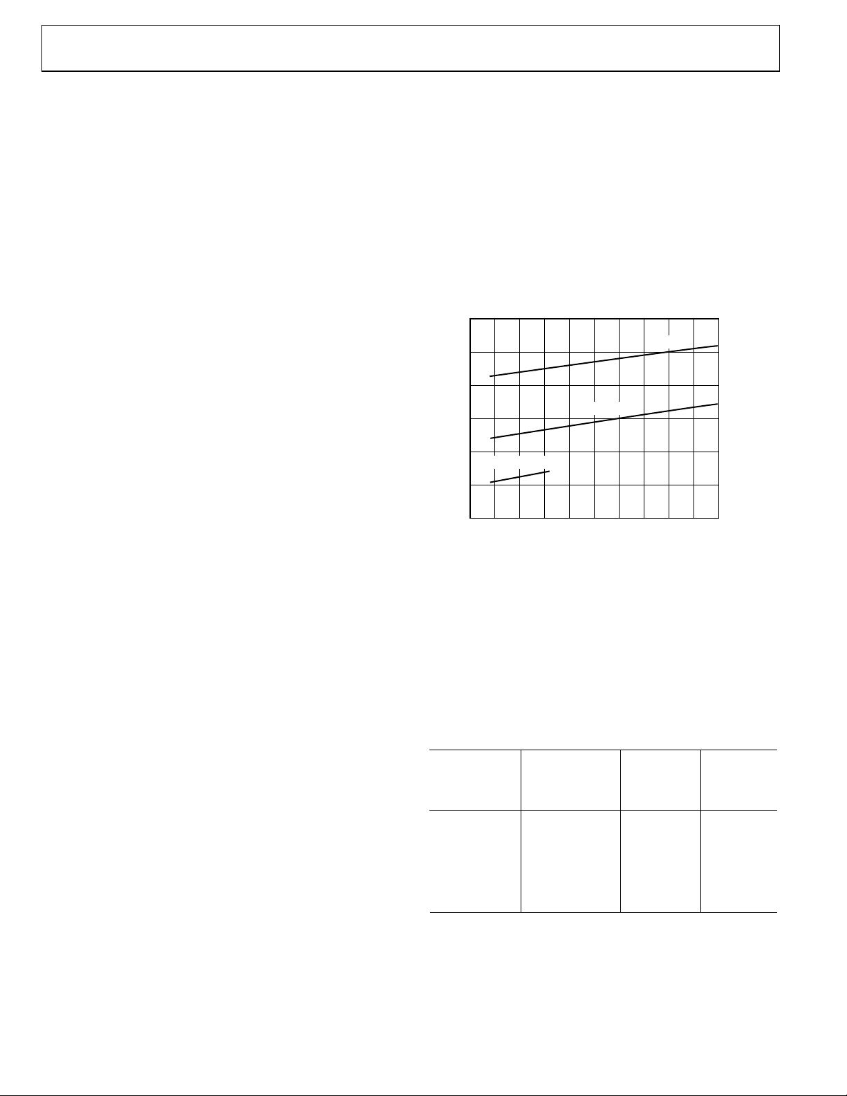
Figure 49 shows the typical analog power dissipation
(ADC_AVDD = 3.3 V) for the ADC versus sampling rate for the
normal power, low power, and ultralow power modes.
INPUT
Either of the ADCs in the AD9863 Rx path can be placed in
),
standby mode independently by writing to the appropriate SPI
register bits in Registers 3, 4, and 5. The minimum standby
power is achieved when both channels are placed in full powerdown mode using the appropriate SPI register bits in Registers
3, 4, and 5. Under this condition, the internal references are
powered down. When either or both of the channel paths are
enabled after a power-down, the wake-up time is directly related
to the recharging of the REFT and REFB decoupling capacitors
and the duration of the power-down. Typically, it takes
approximately 5 ms to restore full operation with fully
discharged 0.1 µF and 10 µF decoupling capacitors on REFT
and REFB.
120
100
80
60
40
AVDD CURRENT (mA)
ULTRALOW POWER
20
0
0 5 10 15 20 25 30 35 40 45 50
Figure 49. Typical Rx Path Analog Supply Current vs. Sample Rate,
V
Rx PATH SAMPLING RATE (MHz)
= 3.3 V for Normal, Low and Ultralow Power Modes
DD
LOW POWER
NORMAL
03604-0-043
Tx PATH BLOCK
The AD9863 transmit (Tx) path includes dual interpolating
12-bit current output DACs that can be operated independently
or can be coupled to form a complex spectrum in an image
reject transmit architecture. Each channel includes two FIR
filters, making the AD9863 capable of 1×, 2×, or 4× interpolation. High speed input and output data rates can be achieved
within the limitations listed in Table 9.
Table 9. AD9863 Tx Path Maximum Data Rate
Input Data
Rate per
Interpolation
Rate
1×
2×
4×
24-Bit Interface
Mode
Channel
(MSPS)
FD, HD12, Clone 80 80
HD24 160 160
FD, HD12, Clone 80 160
HD24 80 160
FD, HD12, Clone 50 200
HD24 50 200
By using the dual DAC outputs to form a complex signal, an
external analog quadrature modulator, such as the Analog
Devices AD8349, can enable an image rejection architecture.
(Note: the AD9863 evaluation board includes a quadrature
modulator in the Tx path that accommodates the AD8345,
AD8346 and the AD8345 footprints.) To optimize the image
rejection capability, as well as LO feedthrough suppression in
DAC
Sampling
Rate
(MSPS)
Rev. 0 | Page 20 of 40
Page 21

AD9863
this architecture, the AD9863 offers programmable (via the SPI
port) fine (trim) gain and offset adjustment for each DAC.
Also included in the AD9863 are a phase-locked loop (PLL)
clock multiplier and a 1.2 V band gap voltage reference. With
the PLL enabled, a clock applied to the CLKIN2 input is
multiplied internally and generates all necessary internal
synchronization clocks. Each 12-bit DAC provides two
complementary current outputs whose full-scale currents can
be determined from a single external resistor.
An external pin, TxPWRDWN, can be used to power down the
Tx path, when not used, to optimize system power consumption.
Using the TxPWRDWN pin disables clocks and some analog
circuitry, saving both digital and analog power. The powerdown mode leaves the biases enabled to facilitate a quick recover y time, typically <10 µs. Additionally, a sleep mode is available,
which turns off the DAC output current, but leaves all other
circuits active, for a modest power savings. An SPI compliant
serial port is used to program the many features of the AD9863.
Note that in power-down mode, the SPI port is still active.
DAC Equivalent Circuits
The AD9863 Tx path consisting of dual 12-bit DACs is shown
in Figure 50. The DACs integrate a high performance TxDAC
core, a programmable gain control through a programmable
gain amplifier (TxPGA), coarse gain control, and offset adjustment and fine gain control to compensate for system mismatches.
Coarse gain applies a gross scaling to either DAC by 1×, (1/2)×,
or (1/11)×. The TxPGA provides gain control from 0 dB to
–20 dB in steps of 0.1 dB and is controlled via the 8-bit TxPGA
setting. A fine gain adjustment of ±4% for each channel is controlled through a 6-bit fine gain register. By default, coarse gain
is 1×, the TxPGA is set to 0 dB, and the fine gain is set to 0%.
The TxDAC core of the AD9863 provides dual, differential,
complementary current outputs generated from the 12-bit data.
The 12-bit dual DACs support update rates up to 200 MSPS.
The differential outputs (IOUT+ and IOUT–) of each dual DAC
are complementary, meaning that they always add up to the
full-scale current output of the DAC, I
. Optimum ac
OUTFS
performance is achieved when the differential current interface
drives balanced loads or a transformer.
OFFSET
DAC
+
TxDAC
REFERENCE
BIAS
TxDAC
Figure 50. TxDAC Output Structure Block Diagram
PGA
PGA
OFFSET
DAC
+
+
+
+
+
+
+
IOUT+A
IOUT–A
IOUT+B
IOUT–B
03604-0-076
The fine gain control provides improved balance of QAM
modulated signals, resulting in improved modulation accuracy
and image rejection.
The independent DAC A and DAC B offset control adds a small
dc current to either IOUT+ or IOUT– (not both). The selection
of which IOUT this offset current is directed toward is
programmable via register setting. Offset control can be used
for suppression of an LO leakage signal that typically results at
the output of the modulator. If the AD9863 is dc-coupled to an
external modulator, this feature can be used to cancel the output
offset on the AD9863 as well as the input offset on the
modulator. The reference circuitry is shown in Figure 51.
REFIO
FSADJ
≥
0.1µFR
SET
4kΩ
1.2V
REFERENCE
Figure 51. Reference Circuitry
DAC A AND DAC B
REFERENCE BIASES
CURRENT
SOURCE ARRAY
I
REF
I
OUTFSMAX
03604-0-077
Referring to the transfer function of the following equation,
I
is the maximum current output of the DAC with the
OUTFSMAX
default gain setting (0 dB), and is based on a reference current,
I
. I
is set by the internal 1.2 V reference and the external
REF
REF
resistor.
R
SET
I
Typical l y, R
optimal dynamic setting for the TxDACs. Increasing R
factor of 2 proportionally decreases I
I
OUTFSMAX
= 64 × (REFIO/R
OUTFSMAX
SET
is 4 kΩ, which sets I
SET
)
OUTFSMAX
to 20 mA, the
OUTFSMAX
by a factor of 2.
of each DAC can be rescaled either simultaneously
SET
by a
using the TxPGA gain register or independently using the
DAC A/DAC B coarse gain registers.
The TxPGA function provides 20 dB of simultaneous gain
range for both DACs, and is controlled by writing to the SPI
register TxPGA gain for a programmable full-scale output of
10% to 100% of I
. The gain curve is linear in dB, with
OUTFSMAX
steps of about 0.1 dB. Internally, the gain is controlled by
changing the main DAC bias currents with an internal TxPGA
DAC whose output is heavily filtered via an on-chip R-C filter
to provide continuous gain transitions. Note that the settling
time and bandwidth of the TxPGA DAC can be improved by a
factor of 2 by writing to the TxPGA fast register.
Each DAC has independent coarse gain control. Coarse gain
control can be used to accommodate different I
OUTFS
from the
dual DACs. The coarse full-scale output control can be adjusted
by using the DAC A/DAC B coarse gain registers to 1/2 or 1/11
of the nominal full-scale current.
Fine gain controls and dc offset controls can be used to
compensate for mismatches (for system level calibration),
allowing improved matching characteristics of the two Tx
Rev. 0 | Page 21 of 40
Page 22

AD9863
channels and aiding in suppressing LO feedthrough. This is
especially useful in image rejection architectures. The 10-bit dc
offset control of each DAC can be used independently to provide an offset of up to ±12% of I
pin, thus allowing calibration of any system offsets. The fine
gain control with 5-bit resolution allows the I
DAC to be varied over a ±4% range, allowing compensation of
any DAC or system gain mismatches. Fine gain control is set
through the DAC A/DAC B fine gain registers, and the offset
control of each DAC is accomplished using the DAC A/DAC B
offset registers.
Clock Input Configuration
The quality of the clock and data input signals is important in
achieving optimum performance. The external clock driver
circuitry provides the AD9863 with a low jitter clock input that
meets the min/max logic levels while providing fast edges.
When a driver is used to buffer the clock input, it should be
placed very close to the AD9863 clock input, thereby negating
any transmission line effects such as reflections due to
mismatch.
Programmable PLL
CLKIN2 can function either as an input data rate clock (PLL
enabled) or as a DAC data rate clock (PLL disabled).
The PLL clock multiplier and distribution circuitry produce the
necessary internal timing to synchronize the rising edge triggered latches for the enabled interpolation filters and DACs.
This circuitry consists of a phase detector, charge pump, voltage
controlled oscillator (VCO), and clock distribution block, all
under SPI port control. The charge pump, phase detector, and
VCO are powered from PLL_AVDD, while the clock distribution circuits are powered from the DVDD supply.
To ensure optimum phase noise performance from the PLL
clock multiplier circuits, PLL_AVDD should originate from a
clean analog supply. The speed of the VCO within the PLL also
has an effect on phase noise.
The PLL locks with VCO speeds as low as 32 MHz up to
350 MHz, but optimal phase noise with respect to VCO speed is
achieved by running it in the range of 64 MHz to 200 MHz.
Power Dissipation
The AD9863 Tx path power is derived from three voltage
supplies: AVDD, DVDD, and DRVDD.
IDRVDD and IDVDD are very dependent on the input data
rate, the interpolation rate, and the activation of the internal
digital modulator. IAVDD has the same type of sensitivity to
data, inter polation rate, and the modulator function, but to a
much lesser degree (< 10%).
Sleep/Power-Down Modes
The AD9863 provides multiple methods for programming
power saving modes. The externally controlled TxPWRDWN
or SPI programmed sleep mode and full power-down mode are
the main options.
to either differential
OUTFSMAX
OUTFSMAX
of each
TxPWRDWN is used to disable all clocks and much of the
analog circuitry in the Tx path when asserted. In this mode, the
biases remain active, therefore reducing the time required for
re-enabling the Tx path. The time of recovery from powerdown for this mode is typically less than 10 µs.
Sleep mode, when activated, turns off the DAC output currents,
but the rest of the chip remains functioning. When coming out
of sleep mode, the AD9863 immediately returns to full operation.
A full power-down mode can be enabled through the SPI
register, which turns off all Tx path related analog and digital
circuitry in the AD9863. When returning from full power-down
mode, enough clock cycles must be allowed to flush the digital
filters of random data acquired during the power-down cycle.
Interpolation Stage
Interpolation filters are available for use in the AD9863 transmit
path, providing 1× (bypassed), 2×, or 4× interpolation.
The interpolation filters effectively increase the Tx data rate
while suppressing the original images. The interpolation filters
digitally shift the worst-case image further away from the
desired signal, thus reducing the requirements on the analog
output reconstruction filter.
There are two 2× interpolation filters available in the Tx path.
An interpolation rate of 4× is achieved using both interpolation
filters; an interpolation rate of 2× is achieved by enabling only
the first 2× interpolation filter.
The first interpolation filter provides 2× interpolation using a
39-tap filter. It suppresses out-of-band signals by 60 dB or more
and has a flat pass-band response (less than 0.1 dB ripple)
extending to 38% of the input Tx data rate (19% of the DAC
update rate, f
). The maximum input data rate is 80 MSPS per
DAC
channel when using 2× interpolation.
The second interpolation filter provides an additional 2× interpolation for an overall 4× interpolation. The second filter is a 15-tap
filter, which suppresses out-of-band signals by 60 dB or more.
The flat pass-band response (less than 0.1 dB attenuation) is
38% of the Tx input data rate (9.5% of f
). The maximum
DAC
input data rate per channel is 50 MSPS per channel when using
4× interpolation.
Latch/Demultiplexer
Data for the dual-channel Tx path can be latched in parallel
through two ports in half-duplex operations (HD24 mode) or
through a single port by interleaving the data (FD, HD12, and
Clone modes). See the Flexible I/O Interface Options section in
the Digital Block description that follows and the Clock
Distribution Block section for further descriptions of each
mode.
Rev. 0 | Page 22 of 40
Page 23
AD9863
DIGITAL BLOCK
The AD9863 digital block allows the device to be configured in
various timing and operation modes. The following sections
discuss the flexible I/O interfaces, the clock distribution block,
and the programming of the device through mode pins or SPI
registers.
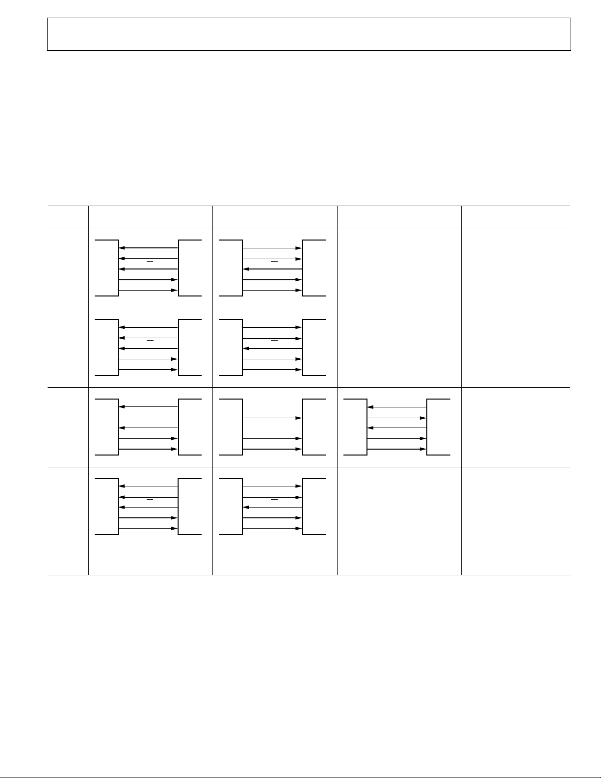
Table 10. Flexible Data Interface Modes
Mode
Name Tx Only Mode (Half-Duplex) Rx Only Mode (Half-Duplex)
HD24
HD12
FD
Clone
AD9863
U[0:11]
L[0:11]
IFACE1
IFACE2
IFACE3
AD9863
U[0:11]
L[11]
IFACE1
IFACE2
IFACE3
AD9863
U[0:11]
L[0:11]
IFACE1
IFACE2
IFACE3
AD9863
U[0:11]
L[11]
IFACE1
IFACE2
IFACE3
Tx_A DATA
Tx_B DATA
Tx/Rx
OUTPUT CLOCK
OUTPUT CLOCK
Tx_A/B DATA
TxSYNC
Tx/Rx
OUTPUT CLOCK
OUTPUT CLOCK
Tx_A/B DATA
TxSYNC
OUTPUT CLOCK
OUTPUT CLOCK
Tx_A/B DATA
TxSYNC
Tx/Rx
OUTPUT CLOCK
OUTPUT CLOCK
DIGITAL
BACK
END
03604-0-078
DIGITAL
BACK
END
03604-0-079
DIGITAL
BACK
END
03604-0-080
DIGITAL
BACK
END
03604-0-081
AD9863
L[0:11]
U[0:11]
IFACE1
IFACE2
IFACE3
AD9863
U[11]
L[0:11]
IFACE1
IFACE2
IFACE3
AD9863
U[0:11]
L[0:11]
IFACE1
IFACE2
IFACE3
AD9863
U[0:11]
L[0:11]
IFACE1
IFACE2
IFACE3
Rx_A DATA
Rx_B DATA
Tx/Rx
OUTPUT CLOCK
OUTPUT CLOCK
RxSYNC
Rx_A/B DATA
Tx/Rx
OUTPUT CLOCK
OUTPUT CLOCK
Rx_A/B DATA
OUTPUT CLOCK
OUTPUT CLOCK
Rx_A DATA
Rx_B DATA
Tx/Rx
OUTPUT CLOCK
OUTPUT CLOCK
Flexible I/O Interface Options
The AD9863 can accommodate various data interface transfer
options (flexible I/O). The AD9863 uses two 12-bit buses, an
upper bus (U12) and a lower bus (L12), to transfer the dualchannel 12-bit ADC data and dual-channel 12-bit DAC data by
means of interleaved data, parallel data, or a mix of both. Table 10
shows the different I/O configurations of the modes depending
on half-duplex or full-duplex operation. Table 11and Table 12
summarize the pin configurations versus the modes.
DIGITAL
BACK
END
03604-0-082
DIGITAL
BACK
END
03604-0-083
DIGITAL
BACK
END
03604-0-084
DIGITAL
BACK
END
03604-0-085
Concurrent Tx + Rx Mode
(Full-Duplex)
N/A
N/A
AD9863
U[0:11]
L[0:11]
IFACE1
IFACE2
IFACE3
Tx_A/B DATA
Rx_A/B DATA
TxSYNC
OUTPUT CLOCK
OUTPUT CLOCK
N/A
DIGITAL
BACK
END
03604-0-086
General Notes
Rx Data Rate
= 1 × ADC Sample Rate
Two 12-Bit Parallel Rx Data
Buses
Tx Data Rate
= 1 × ADC Sample Rate
Two 12-Bit Parallel Tx Data
Buses
Rx Data Rate
= 2 × ADC Sample Rate
One 12-Bit Interleaved Rx
Data Bus
Tx Data Rate
= 2 × ADC Sample Rate
One 12-Bit Interleaved Tx
Data Bus
Rx Data Rate
= 2 × ADC Sample Rate
One 12-Bit Interleaved Rx
Data Bus
Tx Data Rate
= 2 × ADC Sample Rate
One 12-Bit Interleaved Tx
Data Bus
Rx Data Rate
= 1 × ADC Sample Rate
Two 12-Bit Parallel Rx Data
Buses
Tx Data Rate
= 2 × ADC Sample Rate
One 12-Bit Interleaved Tx
Data Bus
Requires SPI Interface to
Configure; Similar to AD9862
Data Interface
Rev. 0 | Page 23 of 40
Page 24

AD9863
Table 11 describes AD9863 pin function (when mode pins are used) relative to I/O mode, and for half-duplex modes whether
transmitting or receiving.
Table 11. AD9863 Pin Function vs. Interface Mode (No SPI Cases)
Mode Name U12 Bus L12 Bus IFACE1 IFACE2 IFACE3
FD Interleaved Tx Data Interleaved Rx Data TxSYNC Buffered Rx Clock Buffered Tx Clock
HD12
Rx = High)
(Tx/
HD12
Rx = Low)
(Tx/
HD24
(Tx/
Rx = High)
HD24
Rx = Low)
(Tx/
Clone Mode
Rx = High)
(Tx/
Clone Mode
Rx = Low)
(Tx/
Interleaved Tx Data
MSB = RxSYNC
Others = Three-state
Tx_A Data Tx_B Data
Rx_B Data Rx_A Data
Clone mode not available without SPI.
Clone mode not available without SPI.
MSB = TxSYNC
Others = Three-state
Interleaved Rx Data
Rx = Tied High 12/24 Pin Control Tied High
Tx/
Rx = Tied Low 12/24 Pin Control Tied High
Tx/
Rx = Tied High 12/24 Pin Control Tied Low
Tx/
Rx = Tied Low 12/24 Pin Control Tied Low
Tx/
Table 12 describes AD9863 pin function (when SPI programming is used) relative to flexible I/O mode, and for half-duplex modes
whether transmitting or receiving.
Table 12. AD9863 Pin Function vs. Interface Mode (Configured through the SPI Registers)
Mode Name U12 Bus L12 Bus IFACE1 IFACE2 IFACE3
FD Interleaved Tx Data Interleaved Rx Data TxSYNC
HD12, Tx Mode
(Tx/
Rx = High)
HD12, Rx Mode
Rx = Low)
(Tx/
HD24, Tx Mode
Rx = High)
(Tx/
HD24, Rx Mode
(Tx/
Rx = Low)
Clone Mode ,
Tx Mode
(Tx/
Rx = High)
Clone Mode ,
Rx Mode
(Tx/
Rx = Low)
Interleaved Tx Data
MSB = RxSYNC
Other = Three-state
Tx_A Data Tx_B Data
Rx_B Data Rx_A Data
Interleaved Tx Data
Rx_B Data Rx_A Data
MSB = TxSYNC
Others = Three-state
Interleaved Tx Data
MSB = TxSYNC
Others = Three-state
Rx = Tied High Optional Buffered
Tx/
Rx = Tied Low Optional Buffered
Tx/
Rx = Tied High Optional Buffered
Tx/
Rx = Tied Low Optional Buffered
Tx/
Rx = Tied High Optional Buffered
Tx/
Rx = Tied Low Optional Buffered
Tx/
Buffered System
Clock
System Clock
System Clock
System Clock
System Clock
System Clock
System Clock
Buffered Tx Clock
Buffered Rx Clock
Buffered Tx Clock
Buffered Rx Clock
Buffered Tx Clock
Buffered Tx Clock
Buffered Rx Clock
Buffered Tx Clock
Buffered Rx Clock
Buffered Tx Clock
Buffered Rx Clock
Summary of Flexible I/O Modes
FD Mode
The full-duplex (FD) mode can be configured by using mode
pins or with SPI programming. Using the SPI allows additional
configuration flexibility of the device.
FD mode is the only mode that supports full-duplex, receive,
and transmit concurrent operation. The upper 12-bit bus (U12)
is used to accept interleaved Tx data, and the lower 12-bit bus
(L12) is used to output interleaved Rx data. Either the Rx path
or the Tx path (or both) can be independently powered down
using either (or both) the RxPwrDwn and TxPwrDwn pins. FD
mode requires interpolation of 2× or 4×.
Rev. 0 | Page 24 of 40
The following notes provide a general description of the FD
mode configuration. For more information, refer to Table 15.
Note the following about the Tx path in FD mode:
• Interpolation rate of 2× or 4× can be programmed with
mode pins or SPI.
• Max DAC update rate = 200 MSPS.
Max Tx input data rate = 80 MSPS/channel (160 MSPS
interleaved).
• TxSYNC is used to direct Tx input data.
TxSYNC = high indicates channel Tx_A data.
TxSYNC = low indicates channel Tx_B data.
Page 25

AD9863
• Buffered Tx clock output (from IFACE3 pin) equals 2× the
DAC update rate; one rising edge per interleaved Tx sample.
Note the following about the Rx path in FD mode:
• Interleaved Rx data output from L12 bus.
• Rx_A output when IFACE2 (or RxSYNC) logic level = low.
Rx_B output when IFACE2 (or RxSYNC) logic level = high.
• ADC CLK Div register can be used to divide down the
clock driving the ADC, which accepts up to 50 MHz.
• Max ADC sampling rate = 50 MSPS.
• The Rx path output data rate is 2× the ADC sample rate
(interleaved).
• Rx_A output when IFACE2 logic level = low.
Rx_B output when IFACE2 logic level = high.
HD12 Mode
The half-duplex, 12-bit interleaved outputs mode, HD12 can be
configured using mode pins or the SPI.
HD12 mode supports half-duplex only operations and can
interface to a single 12-bit data bus with independent Rx and Tx
synchronization pins (RxSYNC and TxSYNC). Both the U12
and L12 buses are used on the AD9863, but the logic level of the
Tx/
selector (controlled through IFACE1 pin) is used to
Rx
disable and three-state the unused bus, allowing U12 and L12 to
be tied together. The MSB of the unused bus acts as the RxSYNC
(during Rx operation) or TxSYNC (during Tx operation). A
single pin is used to output the clocks for Rx and Tx data
latching (from the IFACE3 pin) switching, depending on which
path is enabled. HD12 mode requires interpolation of 2× or 4×.
The following notes provide a general description of the HD12
mode configuration. For more information, refer to Table 15.
Note the following about the Tx path in HD12 mode:
• Interpolation rate of 2× or 4× can be programmed with
mode pins or SPI.
• Interleaved Tx data accepted on U12 bus, L12 bus MSB acts
as TxSYNC.
• Max DAC update rate = 200 MSPS.
Max Tx input data rate = 80 MSPS/channel (160 MSPS
interleaved).
• TxSYNC is used to direct Tx input data.
TxSYNC = high indicates channel Tx_A data.
TxSYNC = low indicates channel Tx_B data.
Note the following about the Rx path in HD12 mode:
• ADC CLK Div register can be used to divide down the
clock driving the ADC, which accepts up to 50 MHz.
• Max ADC sampling rate = 50 MSPS.
• Output data rate = 2× ADC sample rate.
Rev. 0 | Page 25 of 40
HD24 Mode
The half-duplex 24-bit parallel output, HD24, can be configured
using mode pins or through SPI programming.
HD24 mode supports half-duplex only operations and can
interface to a single 24-bit data bus (two parallel 12-bit buses).
Both the U12 and L12 buses are used on the AD9863. The logic
level of the Tx/
used to configure the buses as Rx outputs (during Rx operation)
or as Tx inputs (during Tx operation). A single pin is used to
output the clocks for Rx and Tx data latching (from the IFACE3
pin) switching depending which path is enabled.
The following notes provide a general description of the HD24
mode configuration. For more information, refer to Table 15.
Note the following about the Tx path in HD24 mode:
• Interpolation rate of 1×, 2×, or 4× can be programmed with
mode pins or SPI.
• Max DAC update rate = 200 MSPS.
Max Tx input data rate = 160 MSPS/channel with bypassed
interpolation filters, 100 MSPS for 2× interpolation or
50 MSPS for 4× interpolation.
• Tx_A DAC data is accepted from the U12 bus; Tx_B DAC
data is accepted from the L12 bus.
Note the following about the Rx path in HD24 mode:
• ADC CLK Div register can be used to divide down the
clock driving the ADC, which accepts up to 50 MHz.
• Max ADC sampling rate = 50 MSPS.
• The Rx_A output data is output on L12 bus; the Rx_B
output data is output on U12 bus.
Clone Mode
Clone mode is an interface mode that provides a similar
interface to the AD9860 when used in half-duplex mode. This
mode requires SPI to configure.
Clone mode provides a parallel Rx data output (24 bits) while in
Rx mode, and accepts interleaved Tx data (12-bit) while in Tx
mode. Both the U12 and L12 buses are used on the AD9863.
The logic level of the Tx/
IFACE1 pin) is used to configure the buses for Rx outputs
(during Rx operation) or as Tx inputs (during Tx operation). A
single pin is used to output the clocks for Rx and Tx data
latching (from the IFACE3 pin), depending upon which path is
enabled. Clone mode requires interpolation of 2× or 4×.
selector (controlled through IFACE1 pin) is
Rx
selector (controlled through the
Rx
Page 26

AD9863
The following notes provide a general description of the clone
mode configuration. For more information, refer to Table 15.
• Output data rate = ADC sample rate, that is, two 12-bit
parallel outputs per one buffer Rx clock output cycle.
Note the following about the Tx path in clone mode:
• Interpolation rate of 2× or 4× can be programmed with
mode pins or SPI.
• Max DAC update rate = 200 MSPS.
Max Tx input data rate = 80 MSPS/channel (160 MSPS
interleaved).
• TxSYNC is used to direct Tx input data.
TxSYNC = high indicates channel Tx_A data.
TxSYNC = low indicates channel Tx_B data.
• Buffered Tx clock output (from IFACE3 pin) uses one
rising edge per interleaved Tx sample.
Note the following about the Rx path in clone mode:
• ADC CLK Div register can be used to divide down the
clock driving the ADC, which accepts up to 50 MHz.
• Max ADC sampling rate = 50 MSPS.
Table 13. Mode Pin Names and Functions
Pin Name Duration Function
RxPwrDwn Permanent
TxPwrDwn Permanent
Tx/Rx (IFACE1) Permanent only for
HD Flex I/O interface
ADC_LO_PWR
SPI_Bus_Enable
(SPI_CS)
FD/HD Defined at Reset or
12/24
Only valid for HD
mode
Interp0 and
Interp1
Defined at Reset or
Power-Up
Defined at Reset or
Power-Up
Power-Up
Defined at Reset or
Power-Up
Defined at Reset or
Power-Up
When high, digital clocks to the Rx block are disabled. Analog circuitry that requires <10 µs
to power up are powered off.
When high, digital clocks to Tx block are disabled (PLL remains powered). Analog circuitry
that requires <10 µs to power up are powered off.
When high, digital clocks to Tx block are disabled (PLL remains powered to maintain output
clock with an optional SPI shut off). Tx analog circuitry remains powered up unless
Tx_PwrDwn is asserted.
When low, digital clocks to Rx block are disabled. Rx analog circuitry remains powered up
unless Rx_PwrDwn is asserted.
When enabled, this bit scales the ADC power-down by 40%.
This function is controlled through the SPI_CS pin. This pin must remain low to maintain
mode pin functionality (the SPI port remains nonfunctional). This pin must be high when
coming out of reset to enable the SPI.
Configures the flex I/O for FD or HD mode. This control applies only if the SPI bus is disabled.
If the flex I/O bus is in HD mode, this bit is used to configure parallel or interleaved data
mode. This control applies only if the SPI bus is disabled.
The Interp1 and Interp0 bits configure the PLL and the interpolation rate to 1× [00], 2× [01],
or 4× [10]. This control applies only if the SPI bus is disabled.
• The Rx_A output data is output on L12 bus; the Rx_B
output data is output on U12 bus.
Configuring with Mode Pins
The flexible interface can be configured with or without the SPI,
although more options and flexibility are available when using
the SPI to program the AD9863. Mode pins can be used to
power down sections of the device, reduce overall power
consumption, configure the flexible I/O interface, and program
the interpolation setting. The SPI register map, which provides
many more options, is discussed in the Configuring with SPI
section.
Mode Pins/Power-Up Configuration Options
Mode pins provide various options that are configurable at
power-up. Control pins also provide options for power-down
modes. The logic value of the configuration mode pins are
latched when the device is brought out of reset (rising edge of
). The mode pin names and their functions are shown in
RESET
Table 13. Table 14 provides a detailed description of the mode
pins.
Rev. 0 | Page 26 of 40
Page 27

AD9863
Table 14. Mode Pin Names and Descriptions
Pin Name Description
ADC_LO_PWR
FD/HD (SDO) For flex I/O fonfiguration, this control applies only if the SPI bus is disabled. FD/HD (SDO) is latched during the
12/ 24 For flex I/O configuration, The 12/24 pin control applies only if the SPI bus is disabled and the device is
SPI_Bus_Enable (SPI_CS)
Interp0 and Interp1
RxPwrDwn
TxPwrDwn
Tx/Rx Power-Down Control. Tx/Rx pin enables the appropriate Tx or Rx path in the half-duplex mode.
ADC Low Power Mode Option. ADC_LO_PWR is latched during the rising edge of
Logic low results in ADC operation at nominal power mode.
Logic high results in ADC consuming 40% less power than the nominal power mode.
rising edge of
Logic low setting identifies that the DUT flex I/O port will be configured for half-duplex operation.
12/
24 (IFACE2) is also latched during the rising edge of RESET to identify interleaved data mode or parallel data
mode.
Logic low indicates that the flex I/O will configure itself for parallel data mode.
Logic high indicates that the flex I/O will configure itself for interleaved data mode.
configured for HD mode. 12/
24 (IFACE2) is used to identify interleaved data mode or parallel data modes.
12/
Logic low indicates that the flex I/O will configure itself for HD24 mode.
Logic high indicates that the flex I/O will configure itself for HD12 mode.
SPI_CS is latched during the rising edge of
Logic low results in the SPI being disabled; SPI_DIO, SPI_CLK, and SPI_SDO act as mode pins configuration pins.
Logic high results in the SPI being fully operational; some of the mode pins will be disabled.
Interpolation/PLL Factor Configuration. This control applies only if the SPI bus is disabled.
SPI_DIO (Interp1) and SPI_CLK (Interp0) configure the Tx path for 1× [00], 2× [01], or 4× [10] interpolation and
also enable the PLL of the same multiplication factor.
Power-Down Control. RxPwrDwn logic level controls the power-down function of the Rx path.
Logic low results in the Rx path operating at normal power levels.
Logic high disables the ADC clock and disables some bias circuitry to reduce power consumption.
Power-Down Control. TxPwrDwn logic level controls the power-down function of the Tx path.
Logic low results in the Tx path operating at normal power levels.
Logic high disables the DAC clocks and disables some bias circuitry to reduce power consumption.
Logic low disables the Tx path and enables the Rx path.
Logic high disables the Rx path, and enables the Tx path.
RESET.
24 is latched during the rising edge of RESET.
RESET.
RESET.
Rev. 0 | Page 27 of 40
Page 28

AD9863
Configuring with SPI
The flexible interface can be configured with register settings. Using the register allows more device programmability. Table 15 shows the
required register writes to configure the AD9863 for FD, optional FD, HD24, optional HD24, HD12, optional HD12, and clone mode.
Note that for modes that use interleaved data buses, enabling 2× or 4× interpolation is required.
Table 15. Registers for Configuring SPI
Register Address Setting Description
FD, Mode 1
Register 0x01 [7:5] [000]; clk_mode—Configures timing mode.
Register 0x14 [4] High SpiFDnHD—Configures FD mode.
Register 0x14 [2] High SpiB12n24—Configures FD mode.
Register 0x13 [1:0] [01] or [10] Interpolation Control—Configures 2× or 4× interpolation.
Optional FD, Mode 2
Register 0x01 [7:5] [001] clk_mode—Configures timing mode.
Register 0x14 [4] High SpiFDnHD—Configures FD mode.
Register 0x14 [2] High SpiB12n24—Configures FD mode.
Register 0x13 [1:0] [01] or [10] Interpolation Control—Configures 2× or 4× interpolation.
HD24, Mode 4
Register 0x01 [7:5] [000]; clk_mode—Configures timing mode.
Register 0x14 [4] Low SpiFDnHD—Configures HD mode.
Register 0x14 [2] Low SpiB12n24—Configures HD24 mode.
Register 0x13 [1:0] [00], [01] or [10] Interpolation Control—Configures 1×, 2×, or 4× interpolation.
Optional HD24, Mode 5
Register 0x01 [7:5] [011] clk_mode—Configures timing mode.
Register 0x14 [4] Low SpiFDnHD—Configures HD mode.
Register 0x14 [2] Low SpiB12n24—Configures HD24 mode.
Register 0x13 [1:0] [00], [01] or [10] Interpolation Control—Configures 1×, 2×, or 4× interpolation.
HD12, Mode 7
Register 0x01 [7:5] [000] clk_mode—Configures timing mode.
Register 0x14 [4] Low SpiFDnHD—Configures HD mode.
Register 0x14 [2] High SpiB12n24—Configures HD12 mode.
Register 0x13 [1:0] [01] or [10] Interpolation Control—Configures 2× or 4× interpolation.
Optional HD12, Mode 8
Register 0x01 [7:5] [101] clk_mode—Configures timing mode.
Register 0x14 [4] Low SpiFDnHD—Configures HD mode.
Register 0x14 [2] High SpiB12n24—Configures HD12 mode.
Register 0x13 [1:0] [01] or [10] Interpolation Control—Configures 2× or 4× interpolation.
Clone, Mode 10
Register 0x01 [7:5] [111] clk_mode—Configures timing mode.
Register 0x14 [0] High SpiClone—Configures clone mode.
Register 0x13 [1:0] [01] or [10] Interpolation Control—Configures 2× or 4× interpolation.
Rev. 0 | Page 28 of 40
Page 29

AD9863
SPI Register Map
Registers 0x00 to 0x29 of the AD9863 provide flexible operation of the device. The SPI allows access to many configurable options.
Detailed descriptions of the bit functions are found in Table 17.
Table 16. Register Map
Reg. Name
General 0x00 SDIO BiDir LSB First Soft Reset
Clock Mode 0x01 clk_mode[2:0] Enable
Power-Down 0x02 Tx Analog TxDigital RxDigital PLL Power-
RxA PowerDown
RxB PowerDown
Rx PowerDown
Rx Path 0x06 Rx_A Twos
Rx Path 0x07 Rx_B Twos
Rx Path 0x08 Rx Ultralow
Rx path 0x09 Rx Ultralow
Rx Path 0x0A Rx Ultralow
Tx Path 0B DAC A Offset [9:2]
Tx Path 0C DAC A Offset [1:0] DAC A Offset
Tx Path 0D DAC A Coarse Gain Control DAC A Fine Gain [5:0]
Tx Path 0E DAC B Offset [9:2]
Tx Path 0F DAC B Offset [1:0] DAC B Offset
Tx Path 10 DAC B Coarse Gain Control DAC B Fine Gain [5:0]
Tx Path 11 TxPGA Gain [7:0]
Tx Path 12 TxPGA Slave
I/O
Configuration
I/O
Configuration
Clock 15 PLL Bypass ADC Clock Div Alt Timing
Clock 16 PLL to IFACE2 PLL Slow
Reg.
Add 7
0x03 Rx_A Analog Rx_A DC Bias
0x04 Rx_B Analog Rx_B DC Bias
0x05 Rx Analog Bias RxRef DiffRef VREF
13 Tx Twos
Complement
14 Dig Loop On SpiFDnHD SpiTxnRx SpiB12n24 SPI IO
6
Power Control
Power Control
Enable
Rx Twos
Complement
5
Complement
Complement
Rx Ultralow
Power Control
Rx Ultralow
Power Control
TxPGA Fast
Tx Inverse
Sample
4
Rx_A Clk
Duty
Rx_B Clk
Duty
Rx Ultralow
Power
Control
Rx Ultralow
Power
Control
Update
Interpolation Control [1:0]
Mode
3
Power
Control
PLL Div5 PLL Multiplier [2:0]
2
IFACE2
clkout
Down
Rx Ultralow
Power
Control
1
Inv clkout
(IFACE3)
PLL Output
Disconnect
Control
0
Direction
Direction
SpiClone
Rev. 0 | Page 29 of 40
Page 30

AD9863
Table 17. Register Bit Descriptions
Register Bit Description
Register 0: General
Bit 7: SDIO BiDir (Bidirectional)
Bit 6: LSB First
Bit 5: Soft Reset
Register 1: Clock Mode
Bits 7–5: Clk Mode
Bit 2: Enable IFACE2 clkout Enables the IFACE2 port to be an output clock. Also inverts the IFACE2 output clock in full-duplex mode.
Bit 1: Inv clkout (IFACE3) Inverts the output clock on IFACE3.
Register 2: Power-Down
Bits 7–5: Tx Analog (PowerDown)
Bit 4: Tx Digital (Power-Down)
Bit 3: Rx Digital (Power-Down)
Bit 2: PLL Power-Down
Bit 1: PLL Output Disconnect
Register 3/4: Rx Power-Down
Bit 7: Rx_A Analog/
Rx_B Analog (Power-Down)
Bit 6: Rx_A DC Bias/
Rx_B DC Bias (Power-Down)
Register 5: Rx Power-Down
Bit 7: Rx Analog Bias (PowerDown)
Default setting is low, which indicates that theSPI serial port uses dedicated input and output lines
(4-wire interface), SDIO and SDO pins, respectively. Setting this bit high configures the serial port to
use the SDIO pin as a bidirectional data pin.
Default setting is low, which indicates MSB first SPI port access mode. Setting this bit high
configures the SPI port access to LSB first mode.
Writing a high to this register resets all the registers to their default values and forces the PLL to
relock to the input clock. The soft reset bit is a one-shot register, and is cleared immediately after
the register write is completed.
These bits represent the clocking interface for the various modes. Setting 000 is default. Setting 111
is used for clone mode. Refer to the Summary of Flexible I/O Modes section for a definition of clone
mode.
Setting Mode
000 Standard FD, HD12, HD24 Clock (Modes 1, 4, 7)
001 Optional FD timing (Mode 2)
010 Not Used
011 Optional HD24 timing (Mode 5)
100 Not Used
101 Optional HD12 timing (Mode 8)
110 Not Used
111 Clone Mode (Mode 10)
Three options are available to reduce analog power consumption for the Tx channels. The first two
options disable the analog output from Tx Channel A or B independently, and the third option
disables the output of both channels and reduces the power consumption of some of the additional analog support circuitry for maximum power savings. With all three options, the DAC bias
current is not powered down so recovery times are fast (typically a few clock cycles). The list below
explains the different modes and settings used to configure them.
Power-Down Option Bits Setting [7:5]
Power-Down Tx A Channel Analog Output [1 0 0]
Power-Down Tx B Channel Analog Output [0 1 0]
Power-Down Tx A and Tx B Analog Outputs [1 1 1]
Default is low, which enables the transmit path digital to operate as programmed through other
registers. By setting this bit high, the digital blocks are not clocked to reduce power consumption.
When enabled, the Tx outputs are static, holding their last update values.
Setting this bit high powers down the digital section of the receive path of the chip. Typically, any
unused digital blocks are automatically powered down.
Setting this register bit high forces the CLKIN2 PLL multiplier to a power-down state. This mode can
be used to conserve power or to bypass the internal PLL. To operate the AD9863 when the PLL is
bypassed, CLKIN2 must be supplied with a clock equal to the fastest Tx path clock.
Setting this register bit high disconnects the PLL output from the clock path. If the PLL is enabled, it
locks or stays locked as normal.
Either ADC or both ADCs can be powered down by setting the appropriate register bit high. The
entire analog circuitry of Rx channel is powered down, including the differential references, input
buffer, and the internal digital block. The band gap reference remains active for quick recovery.
Setting either of these bits high powers down the input common-mode bias network for the
respective channel and requires an input signal to be properly dc-biased. By default, these bits are
low, and the Rx inputs are self-biased to approximately AVDD/2 and accept an ac-coupled input.
Setting this bit high powers down all analog bias circuits related to the receive path (including the
differential reference buffer). Because bias circuits are powered down, an additional power saving,
but also a longer recovery time relative to other Rx power-down options, will result.
Rev. 0 | Page 30 of 40
Page 31

AD9863
Register Bit Description
Bit 6: RxREF (Power-Down)
Bit 5: DiffRef (Power-Down)
Bit 4: VREF (Power-Down)
Registers 6/7: Rx Path
Bit 5: Rx_A Twos Complement/
Rx_B Twos Complement
Bit 4: Rx_A Clk Duty/Rx_B Clk
Duty
Registers 8/9/A: Rx Path
Rx UltraLow Power Control Bits
Registers 0B/0C/0E/0F: Tx Path
DAC A/DAC B Offset
DAC A/DAC B Offset Direction
Register 0D/10: Tx Path
Bits 7, 6: DAC A/DAC B Coarse
Gain Control
Bits 5–0: DAC A/DAC B Fine Gain
MSB, LSB
Register 11: Tx Path
Bits 0–7: TxPGA Gain
MSB, LSB
Register 12: Tx Path
Bit 6: TxPGA Slave Enable
Setting this register bit high powers down internal ADC reference circuits. Powering down these
circuits provides additional power saving over other power-down modes. The Rx path wake-up
time depends on the recovery of these references typically of the order of a few milliseconds.
Setting this bit high powers down the ADC’s differential references, REFT and REFB. Recovery time
depends on the value of the REFT and REFB decoupling capacitors.
Setting this register bit high powers down the ADC reference circuit, VREF. Powering down the Rx
band gap reference allows an external reference to drive the VREF pin setting full-scale range of the
Rx paths.
Default data format for the Rx data is straight binary. Setting this bit high generates twos
complement data.
Setting either of these bits high enables the respective channels on-chip duty cycle stabilizer (DCS)
circuit to generate the internal clock for the Rx block. This option is useful for adjusting for high
speed input clocks with skewed duty cycle. The DCS mode can be used with ADC sampling
frequencies over 40 MHz.
Set all bits high, in combination with asserting the ADC_LO_PWR pin, to reduce the power
consumption of the Rx path by a fourth of normal Rx path power consumption.
These 10-bit, twos complement registers control a dc current offset that is combined with the Tx A
or Tx B output signal. An offset current of up to ±12% IOUTFS (2.4 mA for a 20 mA full-scale output)
can be applied to either differential pin on each channel. The offset current can be used to
compensate for offsets that are present in an external mixer stage, reducing LO leakage at its
output. The default setting is 0x00, no offset current. The offset current magnitude is set by using
the lower nine bits. Setting the MSB high adds the offset current to the selected differential pin,
while an MSB low setting subtracts the offset value.
This bit determines to which of the differential output pins for the selected channel the offset
current is applied. Setting this bit low applies the offset to the negative differential pin. Setting this
bit high applies the offset to the positive differential pin.
These register bits scales the full-scale output current (IOUTFS) of either Tx channel independently.
IOUT of the Tx channels is a function of the RSET resistor, the TxPGA setting, and the coarse gain
control setting.
00 Output current scaling by 1/11
01 Output current scaling by ½
10 No output current scaling
11 No output current scaling
The DAC output curve can be adjusted fractionally through the gain trim control. Gain trim of up to
±4% can be achieved on each channel individually. The gain trim register bits are a twos
complement attention control word.
100000 Maximum positive gain adjustment
111111 Minimum positive gain adjustment
000000 No adjustment (default)
000001 Minimum negative gain adjustment
011111 Maximum negative gain adjustment
This 8-bit, straight binary (Bit 0 is the LSB, Bit 7 is the MSB) register controls for the Tx programmable
gain amplifier (TxPGA). The TxPGA provides a 20 dB continuous gain range with 0.1 dB steps (linear
in dB) simultaneously to both Tx channels. By default, this register setting is 0xFF.
0000 0000 Minimum gain scaling –20 dB
1111 1111 Maximum gain scaling 0 dB
The TxPGA gain is controlled through register TxPGA gain setting and, by default, is updated
immediately after the register write. If this bit is set, the TxPGA gain update is synchronized with the
falling edge of a signal applied to the TxPwrDwn pin and is enabled during the wake-up from
power-down.
Rev. 0 | Page 31 of 40
Page 32

AD9863
Register Bit Description
Bit 4: TxPGA Fast Update (Mode)
Register 13: I/O Configuration
Bit 7: Tx Twos Complement
Bit 6: Rx Twos Complement
Bit 5: Tx Inverse Sample
Bits 1,0: Interpolation Control
Register 14: I/O Configuration
Bit 5: Dig Loop On
Bit 4: SPI_FDnHD
Bit 3: SpiTxnRx
Bit 2: SpiB12n24 Control bit for 12-bit or 24-bit modes. High represents 12-bit mode and low represents 24-bit mode.
Bit 1: SPI IO Control Use in conjunction with SpiTxnRx [Register14, Bit 3] to override external TxnRx pin operation.
Bit 0: SpiClone
Register 15: Clock
Bit 7: PLL_Bypass Setting this bit high bypasses the PLL. When bypassed, the PLL remains active.
Bits 5: ADC Clock Div
Bit 4: Alt Timing Mode
Bit 3: PLL Div5
Bits 2–0: PLL Multiplier
Register 16: Clock
Bit 5: PLL to IFACE2
Bit 2: PLL Slow
The TxPGA fast bit controls the update speed of the TxPGA. When fast update mode is enabled, the
TxPGA provides fast gain settling within a few clock cycles, which may introduce spurious signals at
the output of the Tx path. The default setting for this bit is low, and the TxPGA gives a smooth
transition between gain settings. Fast mode is enabled when this bit is set high.
The default data format for Tx data is straight binary. Set this bit high when providing twos
complement Tx data.
The default data format for Rx data is straight binary. Set this bit high when providing twos
complement Rx data.
By default, the transmit data is sampled on the rising edge of the CLKOUT. Setting this bit high
changes this, and the transmit data are sampled on the falling edge.
These register bits control the interpolation rate of the transmit path. The default settings are both
bits low, indicating that both interpolation filters are bypassed. The MSB and LSB are Address Bits 1
and 0, respectively. Setting binary 01 provides an interpolation rate of 2×; binary 10 provides an
interpolation rate of 4×.
When enabled, this bit enables a digital loop back mode. The digital loop-back mode provides a
means of testing digital interfaces and functionality at the system level. In digital loop-back mode,
the full-duplex interface must be enabled. (Refer to the Flexible I/O Interface Options section.) The
device accepts data from the digital input bus according to the FD mode timing, the data is
processed by using the Tx digital path (including any enabled interpolation filter); the processed
data is then output from the Rx path bus.
Control bit to configure full-duplex (high) or half-duplex (low) interface mode. This register, in
combination with the SpiB12n24 register, configures the interface mode of FD, HD12, or HD24. The
register setting is ignored for clone mode operation. By default, this register is set high, and the
device is in FD mode.
Control bit for transmit or receive mode for the half-duplex clock modes. High represents Tx and
low represents Rx.
Set high when in clone mode (see Flexible I/O Interface Options section for definition of clone
mode). Clk_mode should also be set to binary 111, i.e., [Register 01[7:5] = 111.
By default the ADCs are driven directly from CLKIN1 in normal timing operation or from the PLL
output clock in the alternative timing operation. This bit is used to divide the source of the ADC
clock prior to the ADCs. The default setting is low and performs no division. Setting this bit high
divides the clock by 2.
The timing table in the data sheet describes two timing modes: the normal timing operation mode
and the alternative timing operation mode. The default configuration is normal timing mode and
the CLKIN1 drives the Rx path. In alternative timing mode, the PLL output is used to drive the Rx
path. The alternative operation mode is configured by setting this bit high.
The output of the PLL can be divided by 5 by setting this bit high. By default, the PLL directly drives
the Tx digital path with no division of its output.
These bits control the PLL multiplication factor. A default setting is binary 000, which configures the
PLL to 1× multiplication factor. This register, in combination with the PLL Div5 register, sets the PLL
output frequency. The programmable multiplication factors are
000 1×
001 2×
010 4×
011 8×
100 16×
101 – 111 not used
Setting this bit high switches the IFACE2 output signal to the PLL output clock. It is valid only if
Register 0x01, Bit 2 is enabled or if full-duplex mode is configured.
Changes the PLL loop bandwidth and changes the profile of the phase noise generated from the
PLL clock.
Rev. 0 | Page 32 of 40
Page 33

AD9863
PROGRAMMABLE REGISTERS
The AD9863 contains internal registers that are used to configure
the device. A serial port interface provides read/write access to
the internal registers. Single-byte or dual-byte transfers are
supported, as well as MSB first or LSB first transfer formats. The
AD9863’s serial interface port can be configured as a single pin
I/O (SDIO) or as two unidirectional pins for in/out (SDIO/SDO).
The serial port is a flexible, serial communications port, allowing
easy interface to many industry-standard microcontrollers and
microprocessors.
General Operation of the Serial Interface
By default, the serial port accepts data in MSB first mode and
uses four pins: SEN, SCLK, SDIO, and SDO, by default. SEN is a
serial clock enable pin; SCLK is the serial clock pin; SDIO is a
bidirectional data line; and SDO is a serial output pin.
The first eight SCLK rising edges of each communication cycle
are used to write the instruction byte into the AD9863. The
remaining SCLK edges are for Phase 2 of the communication
cycle. Phase 2 is the actual data transfer between the AD9863
and the system controller. Phase 2 of the communication cycle
is a transfer of one or two data bytes as determined by the
instruction byte. Normally, using one communication cycle in a
multibyte transfer is the preferred method; however, single byte
communication cycles are useful to reduce CPU overhead when
register access requires only one byte. An example of this is to
write the AD9863 power-down bits.
All data input to the AD9863 is registered on the rising edge of
SCLK. All data is driven out of the AD9863 on the falling edge
of SCLK.
SEN is an active low control gating read and write cycles. When
SEN is high, SDO and SDIO go into a high impedance state.
SCLK is used to synchronize SPI read and writes at a maximum
bit rate is 30 MHz. Input data is registered on the rising edge,
and output data transitions are registered on the falling edge.
During write operations, the registers are updated after the 16th
rising clock edge (and 24th rising clock edge for the dual-byte
case). Incomplete write operations are ignored.
SDIO is an input data only pin by default. Optionally, a 3-pin
interface may be configured using the SDIO for both input and
output operations and three-stating the SDO pin. Refer to the
SDIO BiDir bit in Register 0x00 (Table 17).
SDO is a serial output data pin used for readback operations in
4-wire mode and is three-stated when SDIO is configured for
bidirectional operation.
There are two phases to a communication cycle with the AD9863.
Phase 1 is the instruction cycle, which is the writing of an
instruction byte into the AD9863, coincident with the first eight
SCLK rising edges. The instruction byte provides the AD9863
serial port controller with information regarding the data
transfer cycle, which is Phase 2 of the communication cycle. The
Phase 1 instruction byte defines whether the upcoming data
transfer is read or write, the number of bytes in the data transfer
(one or two), and the starting register address for the first byte
of the data transfer.
Instruction Byte
The instruction byte contains the information shown in
Table 18, and the bits are described in detail after the table.
Table 18. Instruction Byte
MSB D6 D5 D4 D3 D2 D1 LSB
R/nW 2/n1
Byte
A5 A4 A3 A2 A1 A0
R/nW—Bit 7 of the instruction byte determines whether a read
or write data transfer will occur after the instruction byte write.
Logic high indicates a read operation. Logic low indicates a
write operation.
2/n1 Byte —Bit 6 of the instruction byte determines the
number of bytes to be transferred during the data transfer cycle
of the communication cycle. Logic high indicates a 2-byte
transfer. Logic low indicates a 1-byte transfer.
A5, A4, A3, A2, A1, A0—Bits 5, 4, 3, 2, 1, and 0 of the
instruction byte determine which register is accessed during the
data transfer portion of the communication cycle. For 2-byte
transfers, this address is the starting byte address. The second
byte address is automatically decremented when the interface is
configured for MSB first transfers. For LSB first transfers, the
address of the second byte is automatically incremented.
Table 19. Serial Port Interface Timing
Maximum SCLK Frequency (f
Minimum SCLK High Pulse Width (t
Minimum SCLK Low Pulse Width (t
Maximum Clock Rise/Fall Time 1 ms
Data to SCLK timing (tDS) 12.5 ns
Data Hold Time (tDH) 0 ns
) 40 MHz
SCLK
) 12.5 ns
PWH
) 12.5 ns
PWL
Rev. 0 | Page 33 of 40
Page 34
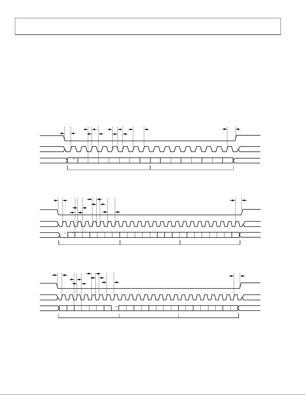
AD9863
SCLK
SCLK
Write Operations
The SPI write operation uses the instruction header to configure a 1-byte or 2-byte register write using the 2/n1 Byte setting.
The instruction byte followed by the register data is written
serially into the device through the SDIO pin on rising edges of
the interface clock, SCLK. The data can be transferred MSB first
or LSB first, depending on the setting of the LSB first register
bit. The write operation is the same regardless of SDIO BiDir
register setting.
Figure 52 to Figure 54 are examples of writing data into the
device. Figure 52 shows a 1 byte write in MSB first mode;
Figure 53 shows a 2-byte write in MSB first mode; and Figure 54
shows a 2-byte write shows in LSB first mode. Note the
differences between LSB and MSB first modes: both the
instruction header and data are reversed, and the second data
byte register location is different. In the default MSB first mode,
the second data byte is written to a decremented register
address. In LSB first mode, the second data byte is written to an
incremented register address.
SEN
SDIO
SEN
SDIO
SEN
DON'T CARE
DON'T CARE
DON'T CARE
t
DS
t
S
R/W
t
DH
2/1 A5 A4 A3 A2 A1 A0 D7 D6 D5 D4 D3 D2 D1 D0
INSTRUCTION HEADER REGISTER DATA
t
HI
t
CLK
t
LO
Figure 52. 1-Byte Serial Register Write in MSB First Mode
t
t
S
t
DH
t
DS
INSTRUCTION HEADER (REGISTER N) REGISTER (N) DATA REGISTER (N–1) DATA
HI
t
LO
t
CLK
A5 A4 A3 A2 A1 A0 D7 D6 D5 D4 D3 D2 D1 D0 D7 D6 D5 D4 D3 D2 D1 D0R/W 2/1
Figure 53. 2-Byte Serial Register Write in MSB First Mode
t
t
S
t
DS
t
DH
t
LO
HI
t
CLK
t
H
DON'T CARE
t
t
H
DON'T CARE
H
DON'T CARE
DON'T CAREDON'T CARE
03604-0-087
03604-0-088
SCLK
SDIO
DON'T CARE
DON'T CARE
A0 A1 A2 A3 A4 A5 D0 D1 D2 D3 D4 D5 D6 D7 D0 D1 D2 D3 D4 D5 D6 D7R/W2/1
INSTRUCTION HEADER (REGISTER N) REGISTER (N) DATA REGISTER (N+1) DATA
Figure 54. 2-Byte Serial Register Write in LSB First Mode
Rev. 0 | Page 34 of 40
DON'T CARE
DON'T CARE
03604-0-089
Page 35

AD9863
Read Operations
The readback of registers can be a single or dual data byte
operation. The readback can be configured to use 3-wire or
4-wire and can be formatted with MSB first or LSB first. The
instruction header is written to the device either MSB or LSB
first (depending on the mode) followed by the 8-bit output data,
appropriately MSB or LSB justified. By default, the output data
is sent to the dedicated output pin (SDO). Three-wire operation
can be configured by setting the SDIO BiDir register. In 3-wire
mode, the SDIO pin will become an output pin after receiving
the 8-bit instruction header with a readback request.
Figure 55 shows 4-wire SPI read with MSB first; Figure 56
shows 3-wire read with MSB first; and Figure 57 shows 4-wire
read with LSB first.
SEN
SCLK
SDIO
SDO
SEN
SCLK
SDIO
SEN
DON'T CARE
DON'T CARE
DON'T CARE
DON'T CARE
t
S
t
DS
t
DH
DON'T CARE
t
HI
t
LO
A5
A4 A3 A2 A1 A0R/W 2/1
INSTRUCTION HEADER
t
CLK
t
DV
DON'T CARE
D7 D6 D5 D4 D3 D2 D1 D0
OUTPUT REGISTER DATA
t
H
Figure 55. 1-Byte Serial Register Readback In MSB First Mode, SDIO BiDir Bit Set Logic Low (Default, 4-Wire Mode)
t
S
t
DS
t
DH
t
HI
t
LO
A5 A4 A3 A2 A1 A0R/W 2/1
t
CLK
t
H
t
DV
OUTPUT REGISTER DATAINSTRUCTION HEADER
Figure 56. 1-Byte Serial Register Readback in MSB First Mode, SDIO BiDir Bit Set Logic High (Default, 3-Wire Mode)
t
S
t
DS
t
DH
t
HI
t
LO
t
CLK
t
DV
t
H
DON'T CARE
DON'T CARE
DON'T CARE
DON'T CARED7 D6 D5 D4 D3 D2 D1 D0
03604-0-090
03604-0-091
SCLK
SDIO
SDO
DON'T CARE
DON'T CARE
A0 A1 A2 A3 A4 A5 R/W
INSTRUCTION HEADER
2/1
DON'T CARE
OUTPUT REGISTER DATA
DON'T CARE
DON'T CAREDON'T CARE D0 D1 D2 D3 D4 D5 D6 D7
03604-0-092
Figure 57. 1-Byte Serial Register Readback in LSB First Mode, SDIO BiDir Bit Set Logic Low (Default, 4-Wire Mode)
Rev. 0 | Page 35 of 40
Page 36

AD9863
CLOCK DISTRIBUTION BLOCK
Theory/Description
The AD9863 uses a PLL clock multiplier circuit and an internal
distribution block to generate all required clocks for various
timing configurations. The AD9863 has two independent input
clocks, CLKIN1 and CLKIN2. The CLKIN1 is primarily used to
drive the Rx ADCs path. The CLKIN2 is primarily used to drive
the TxDACs path. There are many options for configuring the
clock distribution block, which are programmed through
internal register settings. The Clock Distribution Block Diagram
section describes the timing block diagram breakdown, followed
by the data timing for the different data interface options.
The clock distribution block contains a PLL, which includes an
optional output divide-by-5 circuit, an ADC divide-by-2 circuit,
multiplexers, and other digital logic.
There are two main methods of configuring the Rx path timing
of the AD9863, normal timing mode and alternate timing
mode, which are controlled through register Alt timing mode
[Register 0x15, Bit 4]. In normal timing mode, the Rx path clock
is driven directly from the CLKIN1 input and the Tx path is
driven by a clock derived from CLKIN2 multiplied by the onchip PLL. In alternative timing mode, the CLKIN2 drives the
PLL circuitry, and the PLL output clock drives both the Rx path
clock and Tx path clock.
Because alternate timing mode uses the PLL to derive the Rx
path clock, the ADC performance may degrade slightly. This
degradation is due to the phase noise from the PLL, although
typically it is only noticeable in undersampling applications
when the input signal is above the first Nyquist zone of the ADC.
The PLL can provide 1×, 2×, 4×, 8×, and 16× multiplication or
can be bypassed and powered down through register PLL
bypass [Register 0x15, Bit 7] and through register PLL powerdown [Register 0x2, Bit 2]. The PLL requires a minimum input
clock frequency of 16 MHz and needs to provide a minimum
PLL output clock of 32 MHz. This limit applies to the PLL
output prior to the optional divide-by-5 circuitry. For clock
frequencies below these limits, the PLL must be bypassed. The
PLL maximum output frequency before the divide-by-5 circuitry
is 350 MHz. Table 20 shows the input and output clock rates for
all the multiplication settings.
Table 20. PLL Input and Output Minimum and Maximum
Clock Rates
PLL Setting
1× (PLL Bypassed) 1 /200 1 /200
1× (PLL Enabled) 32 /200 32 /200
2× 16 /100 32 /200
4× 16 /50 64 /200
8× 16 /25 128 /200
* 1/5 × 32 /200 6.4 /40
* 2/5 × 16 /175 6.4 /70
* 4/5 × 16 /87.5 12.8 /70
* 8/5 × 16 /43.75 25.6 /70
* 16/5 × 16 /21.875 51.2 /70
* Indicates PLL output divide-by-5 circuit enabled.
CLKIN2 Input
(Min/Max) (MHz)
PLL Output Clock
(Min/Max) (MHz)
Clock Distribution Block Diagram
The clock distribution block diagram is shown in Figure 58. An
output clock formatter configures the output synchronization
signals, IFACE1, IFACE2, and IFACE3. These interface pin
signals depend on clock mode setting, data I/O configuration,
and other operational settings. Clock mode and data I/O
configuration are defined in register settings of clk_mode,
SpiFDnHD, and SpiB12n24.
Table 21 shows the configuration of the IFACE1, IFACE2 and
IFACE3 pins relative to clock mode; for half-duplex cases, the
IFACE1 pin is an input that identifies if the device is in Rx or Tx
operation mode. The clock mode is used to specify the timing
for each data interface operation modes, which are discussed in
detail in the Flexible I/O Interface Options section. The T and R
extensions after the half-duplex Modes 4, 5, 7, 8, and 10 in the
Table 21 indicate that the device is in transmit or receive
operation mode. The default clock mode setting [Register 0x01,
Bits 5–7, clk_mode] of ‘000’ configures clock Mode 1 for the
full-duplex operation, Mode 4 for half-duplex 24 operation and
Mode 7 for half-duplex 12 operation. Modes 2, 5, 8, and 10 are
optional timing configurations for the AD9863 and can be
programmed through Register 0x01 clk_mode.
Rev. 0 | Page 36 of 40
Page 37

AD9863
CLKIN1
1
1, 2, 4, 8, 16
CLKIN2
2
1. ALTERNATE TIMING MODE: REG 0x15, BIT 4
2. PLL MULTIPLICATION SETTING: REG 0x15, BITS 2–0
3. PLL OUTPUT DIVIDE BY 5; REG 0x15, BIT 3
4. Rx PATH DIVIDE BY 2: REG 0x15, BIT 5
5. PLL BYPASS PATH: REG 0x15, BIT 7
6. INTERP CONTROL, Tx/Rx INV IFACE3, CLK MODE, INV IFACE2, FD/HD, 12/24
1, 5
3
Figure 58. Clock Distribution Block Diagram
1, 2
4
50MHz MAX
5
Rx
DIGITAL
BLOCK
Tx
DIGITAL
BLOCK
Rx
PATH
Tx
PATH
OUTPUT
CLOCK
FORMATTER
6
IFACE2
IFACE3
03604-0-093
Table 21. Interface Pins (IFACE1, IFACE2, IFACE3) Configuration Definition for Flexible Interface Operation
Clock
1 2 4T 4R 5T 5R 7T 7R 8T 8R 10T 10R
Mode
Full-Duplex Half-Duplex, 24-Bit Half-Duplex, 12-Bit Clone Mode
CLKIN1
and
CLKIN2
IFACE1
Pin
IFACE2
Pin
IFACE3
Pin
Independent
TxSync
Buff_CLKIN1 RxSync Optional CLKOUT Optional CLKOUT
Tx Clock
Internally
Tied
Together
Independent
Rx
Tx/
Tx
Clock
Rx
Clock
Internally Tied
Together
Tx
Clock
Rx
Clock
Independent
Rx
Tx/
Tx
Clock
Rx
Clock
Internally Tied
Together
Tx
Clock
Rx
Clock
Independent
Rx
Tx/
Optional
CLKOUT
Tx
Clock
Rx
Clock
The Tx clock output frequency depends on whether the data is
in interleaved or parallel (noninterleaved) configuration. Modes
1, 2, 7, 8, and 10 use Tx interleaved data and require either 2× or
4× interpolation to be enabled.
• DAC update rate = CLKIN2 × PLL setting.
• Noninterleaved Tx data clock frequency = CLKIN2 × PLL
setting × 1/(interpolation rate).
• Interleaved Tx data clock frequency = 2 × CLKIN2 × PLL
setting × 1/(interpolation rate).
The Rx clock does not depend on whether the data is
interleaved or parallel, but does depends on the configuration of
the timing mode: normal or alternative.
• Normal timing mode, Rx clock frequency = CLKIN1 ×
ADC Div factor (if enabled).
• Alternative timing mode, Rx clock frequency = CLKIN2 ×
PLL setting × ADC Div factor (if enabled).
Rev. 0 | Page 37 of 40
An optional CLKOUT from IFACE2 is available as a stable
system clock running at the CLKIN1 frequency or the TxDAC
update rate, which is equal to CLKIN2 × PLL setting. Setting the
enable IFACE2 register [Register 0x01, Bit 2] enables the
IFACE2 optional clock output. In FD mode the IFACE2 pin
always acts as a clock output; the enable IFACE2 pin can be
used to invert the IFACE2 output.
Configuration
The AD9863 timing for the transmit path and for the receive
path depend on the mode setting and various programmable
options. The registers that affect the output clock timing and
data input/output timing are clk_mode [2:0]; enable IFACE2;
inv clkout (IFACE3); Tx inverse sample; interpolation control;
PLL bypass; ADC clock div; Alt timing mode; PLL Div5; PLL
multiplication; and PLL to IFACE2. The clk_mode register is
discussed previously. Table 22 shows the other register bits that
are used to configure the output clock timing and data latching
options available in the AD9863.
Page 38
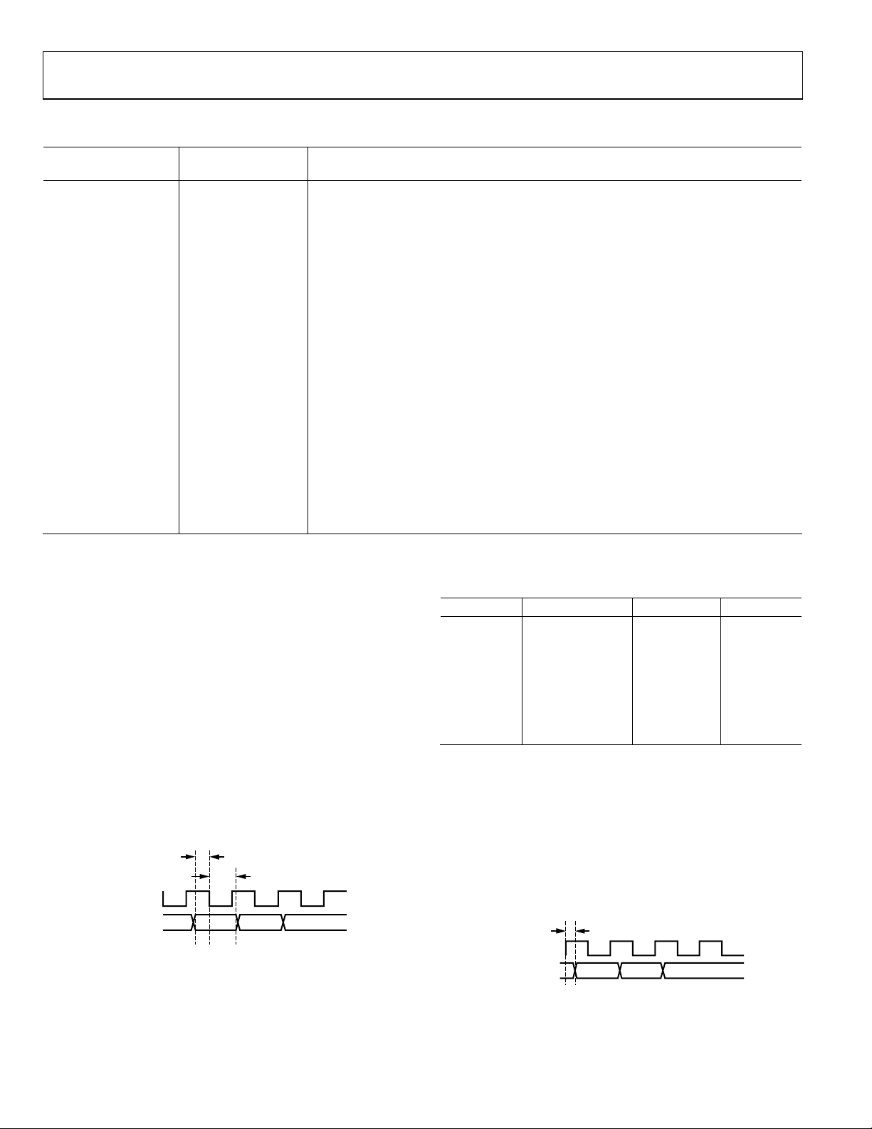
AD9863
Table 22. Serial Registers Related to the Clock Distribution Block
Register Name
Register Address,
Bit(s)
Function
Enable IFACE2 Register 0x01, Bit 2 0: There is no clock output from IFACE2 pin, except in FD mode.
1: The IFACE2 pin outputs a continuous reference clock from the PLL output. In FD mode,
this inverts the IFACE2 output.
Inv clkout (IFACE3) Register 0x01, Bit 1 0: The IFACE3 clock output is not inverted.
1: The IFACE3 clock output is inverted.
Tx Inverse Sample Register 0x13, Bit 5 0: The Tx path data is latched relative to the output Tx clock rising edge.
1: The Tx path data is latched relative to the output Tx clock falling edge.
Interpolation Control Register 0x13, Bit 1:0 Sets interpolation of 1×, 2×, or 4× for the Tx path.
PLL Bypass Register 0x15, Bit 7 0: PLL block is used to generate system clock.
1: PLL block bypasses generate system clock.
ADC Clock Div Register 0x15, Bit 5 0: ADC clock rate equals the Rx path frequency.
1: ADC clock is one-half the Rx path frequency.
Alt Timing Mode Register 0x15, Bit 4 0: CLKIN1 is used to drive the Rx path clock.
1: PLL block output is used to drive the Rx path clock.
PLL Div5 Register 0x15, Bit 3 0: PLL block output clock is not divided down.
1: PLL block output clock is divided by 5.
PLL Multiplier Register 0x15, Bit 2:0
Sets multiplication factor of the PLL block to 1× (000), 2× (001), 4× (010), 8× (011), or 16x
(100).
PLL to IFACE2 Register 0x16, Bit 5 0: If enable IFACE2 register is set, IFACE2 outputs buffered CLKIN.
1: If enable IFACE2 register is set, IFACE2 outputs buffered PLL output clock.
Transmit (Tx) timing requires specific setup and hold times to
properly latch data through the data interface bus. These timing
parameters are specified relative to an internally generated
output reference clock. The AD9863 has two interface clocks
provided through the IFACE3 and IFACE2 pins. The transmit
timing specifications, setup and hold time, provide a minimum
required window of valid data.
Setup time (t
) is the time required for data to initially settle
SETUP
to a valid logic level prior to the relative output timing edge.
Hold time (t
) is the time after the output timing edge that
HOLD
valid data must remain on the data bus to be properly latched.
Figure 59 shows t
SETUP
and t
relative to IFACE3 falling edge.
HOLD
Note that in some cases negative time is specified, for example
with t
timing, which means that the hold time edge occurs
HOLD
before the relative output clock edge.
t
SETUP
t
HOLD
IFACE3 (CLKOUT)
Tx DATA
03604-0-094
Figure 59. Tx Data Timing Diagram
Table 23. Typical Tx Data Latch Timing Relative to
IFACE3 Falling Edge
Mode No. Mode Name t
(ns) t
SETUP
1 FD 5 –2.5
2 Optional FD 5 –2.5
4 HD24 5 –1.5
5 Optional HD24 5 –1.5
7 HD12 5 –2.5
8 Optional HD12 5 –2.5
10 Clone 5 –1.5
Receive (Rx) path data is output after a reference output clock
edge. The time delay of the Rx data relative to a reference output
clock is called the output delay, t
. The AD9863 has two
OD
possible interface clocks provided through the IFACE3 and
IFACE2 pins. Figure 60 shows t
relative to IFACE3 rising
OD
edge. Note that in some cases negative time is specified, which
means that the output data transition occurs prior to the relative
output clock edge.
t
OD
IFACE3 (CLKOUT)
Rx DATA
Table 23 shows typical setup-and-hold times for the AD9863 in
the various mode configurations.
Figure 60. Rx Data Timing Diagram
HOLD
(ns)
03604-0-095
Rev. 0 | Page 38 of 40
Page 39

AD9863
Table 24 shows typical output delay times for the AD9863 in the various mode configurations.
Table 24. AD9863 Rx Data Latch Timing
Mode No. Mode Name tOD Data Delay [ns] Relative to:
1 FD +2.5 ns Relative to IFACE2 rising edge
+1 ns Relative to IFACE3 rising edge
2 Optional FD +1 ns Relative To IFACE3 rising edge
+2 ns IFACE2 (RxSYNC) relative to LSB
4 HD24 −1.5 ns Relative to IFACE3 rising edge
5 Optional HD24 −0.5 ns Relative to IFACE3 rising edge
7 HD12 −1.5 ns Relative to IFACE3 rising edge
8 Optional HD12 +0.5 ns Relative to IFACE3 rising edge
+0 ns U12 (RxSYNC) relative to LSB
10 Clone +1.5 ns Relative to IFACE3 rising edge
Configuration without Serial Port Interface (Using Mode Pins)
The AD9863 can be configured using mode pins if a serial port interface is not available. This section only applies to configuring the
AD9863 without an SPI. Refer to the Digital Block, Configuring with Mode Pins section of the data sheet for more information.
When using the mode pin option, the pins shown in Table 25
are used to configured the AD9863.
Table 25. Using Mode Pin (SPI Disabled) to Configure Timing (SPI_CS, Pin 64, Must be Tied Low)
Clock Mode
Mode 1 (FD) 2×
Mode 4 (HD24) 1×
Mode 7 (HD12)
1
Pin 17 (IFACE2) is an output clock in FD mode.
Interpolation
Setting
4×
2×
4×
2×
4×
PLL Setting
2×
4×
Bypassed
2×
4×
2×
4×
FD/HD
Pin 3
1 N/A
0 0 0, 0
0 1 0, 1
12/20
Pin 17
1
Interp1,Interp0
Pin 1, Pin 2
0, 1
1, 0
0, 1
1, 0
1, 0
Rev. 0 | Page 39 of 40
Page 40

AD9863
OUTLINE DIMENSIONS
9.00
BSC SQ
PIN 1
INDICATOR
0.60 MAX
49
48
0.60 MAX
0.30
0.25
0.18
PIN 1
64
INDICATOR
1
7.25
7.10 SQ*
6.95
16
0.25MIN
1.00
0.85
0.80
12° MAX
SEATING
PLANE
TOP
VIEW
8.75
BSC SQ
0.45
0.40
0.35
0.80 MAX
0.65 TYP
0.50 BSC
*
COMPLIANT TO JEDEC STANDARDS MO-220-VMMD
EXCEPT FOR EXPOSED PAD DIMENSION
0.20 REF
0.05 MAX
0.02 NOM
33
32
BOTTOM
VIEW
7.50 REF
17
Figure 61. 64-Lead Lead Frame Chip Scale Package (LFCSP) [CP-64]
Dimensions shown in millimeters
ORDERING GUIDE
Model Temperature Range Package Description Package Option
AD9863BCP-50
AD9863BCPRL-50
–40°C to +85°C (Ambient)
–40°C to +85°C (Ambient)
AD9863-50EB 25°C (Ambient) Evaluation Board
64-Lead LFCSP CP-64
64-Lead LFCSP CP-64
© 2003 Analog Devices, Inc. All rights reserved. Trademarks and
registered trademarks are the property of their respective owners.
C03604–0–11/03(0)
Rev. 0 | Page 40 of 40
 Loading...