

Page 1
Mixed-Signal Front-End (MxFE™) Processor
a
FEATURES
Mixed-Signal Front-End Processor with Dual Converter
Receive and Dual Converter Transmit Signal Paths
Receive Signal Path Includes:
Two 10-/12-Bit, 64 MSPS Sampling A/D Converters
with Internal or External Independent References,
Input Buffers, Programmable Gain Amplifiers,
Low-Pass Decimation Filters, and a Digital Hilbert Filter
Transmit Signal Path Includes:
Two 12-/14-Bit, 128 MSPS D/A Converters with
Programmable Full-Scale Output Current, Channel
Independent Fine Gain and Offset Control, Digital
Hilbert and Interpolation Filters, and Digitally Tunable
Real or Complex Up-Converters
Delay-Locked Loop Clock Multiplier and Integrated
Timing Generation Circuitry Allow for Single Crystal
or Clock Operation
Programmable Output Clocks, Serial Programmable
Interface, Programmable Sigma-Delta, Three Auxiliary
DAC Outputs and Two Auxiliary ADCs with Dual
Multiplexed Inputs
APPLICATIONS
Broadband Wireless Systems
Fixed Wireless, WLAN, MMDS, LMDS
Broadband Wireline Systems
Cable Modems, VDSL, PowerPlug
Digital Communications
Set-Top Boxes, Data Modems
GENERAL DESCRIPTION
The AD9860 and AD9862 (AD9860/AD9862) are versatile
integrated mixed-signal front-ends (MxFE) that are optimized
for broadband communication markets. The AD9860/AD9862
are cost effective, mixed signal solutions for wireless or wireline
standards based or proprietary broadband modem systems where
dynamic performance, power dissipation, cost, and size are all
critical attributes. The AD9860 has 10-bit ADCs and 12-bit DACs;
the AD9862 has 12-bit ADCs and 14-bit DACs.
The AD9860/AD9862 receive path (Rx) consists of two channels
that each include a high performance, 10-/12-bit, 64 MSPS analogto-digital converter (ADC), input buffer, Programmable Gain
Amplifier (RxPGA), digital Hilbert filter, and decimation filter. The
Rx can be used to receive real, diversity, or I/Q data at baseband or
low IF. The input buffers provide a constant input impedance for
both channels to ease impedance matching with external components (e.g., SAW filter). The RxPGA provides a 20 dB gain
*Protected by U.S.Patent No. 5,969,657; other patents pending.
MxFE is a trademark of Analog Devices, Inc.
REV. 0
Information furnished by Analog Devices is believed to be accurate and
reliable. However, no responsibility is assumed by Analog Devices for its
use, nor for any infringements of patents or other rights of third parties that
may result from its use. No license is granted by implication or otherwise
under any patent or patent rights of Analog Devices.
for Broadband Communications
AD9860/AD9862
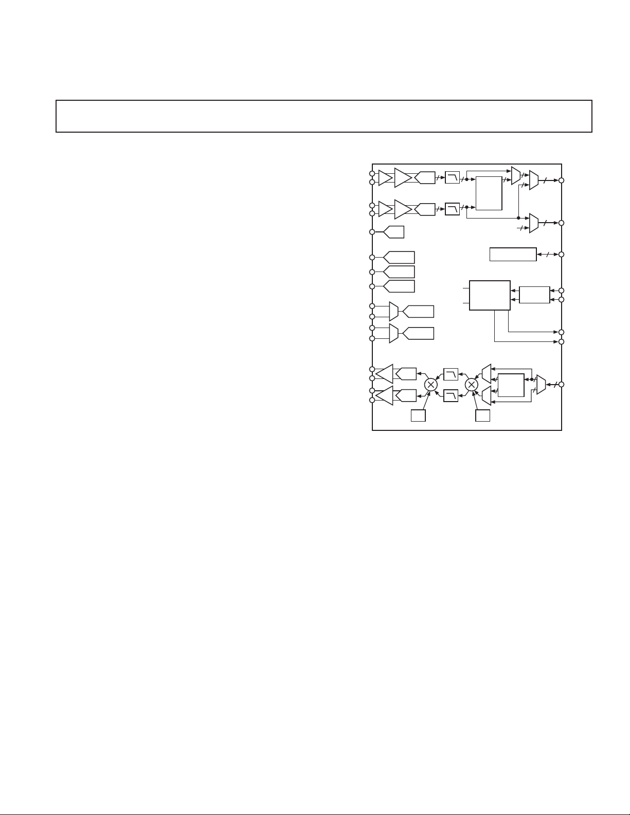
FUNCTIONAL BLOCK DIAGRAM
VIN+A
VIN–A
VIN+B
VIN–B
SIGDELT
AUX _DAC_ A
AUX _DAC_ B
AUX _DAC_ C
AUX_ADC_A1
AUX_ADC_A2
AUX_ADC_B1
AUX_ADC_B2
IOUT+A
IOUT–A
IOUT+B
IOUT–B
range for both channels. The output data bus can be multiplexed to accommodate a variety of interface types.
The AD9860/AD9862 transmit path (Tx) consists of two channels that contain high performance, 12-/14-bit, 128 MSPS
digital-to-analog converters (DAC), programmable gain amplifiers
(TxPGA), interpolation filters, a Hilbert filter, and digital mixers
for complex or real signal frequency modulation. The Tx latch
and demultiplexer circuitry can process real or I/Q data. Interpolation rates of 2 and 4 are available to ease requirements on
an external reconstruction filter. For single channel systems, the
digital Hilbert filter can be used with an external quadrature
modulator to create an image rejection architecture. The two
12-/14-bit, high performance DACs produce an output signal
that can be scaled over a 20 dB range by the TxPGA.
A programmable delay-locked loop (DLL) clock multiplier and
integrated timing circuits enable the use of a single external
reference clock or an external crystal to generate clocking for all
internal blocks and also provides two external clock outputs.
Additional features include a programmable sigma-delta output,
four auxiliary ADC inputs and three auxiliary DAC outputs.
Device programmability is facilitated by a serial port interface
(SPI) combined with a register bank. The AD9860/AD9862 is
available in a space saving 128-lead LQFP.
One Technology Way, P.O. Box 9106, Norwood, MA 02062-9106, U.S.A.
Tel: 781/329-4700www.analog.com
Fax: 781/326-8703 © Analog Devices, Inc., 2002
1x
1x
PGA
PGA
PGA
PGA
-
AUX DAC
AUX DAC
AUX DAC
DAC
DAC
ADC
BYPASSABLE LOW-PASS
DECIMATION FILTER
ADC
AD9860/AD9862
Rx PATH
TIMING
Tx PATH
BYPASSABLE
DIGITAL
QUADRATURE
MIXER
BYPASSABLE
FS/4
LOW-PASS
FS/8
INTERPOLATION
TIMING
BYPASSABLE
QUADRATURE
FILTER
AUX ADC
AUX ADC
HILBERT
FILTER
CLOCK
DISTRIBUTION
BLOCK
DIGITAL
MIXER
NCO
LOGIC LOW
SPI REGISTERS
HILBERT
FILTER
DLL
1, 2, 4
*
RxA DATA
[0:11]
RxB DATA
[0:11]
SPI
INTERFACE
OSC1
OSC2
CLKOUT1
CLKOUT2
Tx DATA
[0:13]
Page 2

AD9860/AD9862–SPECIFICATIONS
(VA = 3.3 V 5%, VD = 3.3 V 10%, f
Normal Timing Mode, 2 DLL Setting, R
= 128 MHz, f
DAC
= 4 k, 50 DAC Load,
SET
= 64 MHz
ADC
RxPGA = +6 dB Gain, TxPGA = +20 dB Gain.)
Tx PARAMETERS Temp Level Min Typ Max Unit
12-/14-BIT DAC CHARACTERISTICS
Resolution NA NA 12/14 Bits
Maximum Update Rate 128 MSPS
Full-Scale Output Current Full I 2 20 mA
Gain Error (Using Internal Reference) 25ºCI –5.5 +0.5 +5.5 %FS
Offset Error 25ºCI –1 0.0 +1 %FS
Reference Voltage (REFIO Level) 25ºCI 1.15 1.22 1.28 V
Negative Differential Nonlinearity (–DNL) 25ºC III –0.5/–0.5 LSB
Positive Differential Nonlinearity (+DNL) 25ºC III 1/2 LSB
Integral Nonlinearity (INL) 25ºC III ±1/±3 LSB
Output Capacitance 25ºC III 5 pF
Phase Noise @ 1 kHz Offset, 6 MHz Tone
Crystal and OSC IN Multiplier Enabled at 4 25ºC III –115 dBc/Hz
Output Voltage Compliance Range Full II –0.5 +1.5 V
TRANSMIT TxPGA CHARACTERISTICS
Gain Range 25ºC III 20 dB
Step Size Accuracy 25ºC III ±0.1 dB
Step Size 25ºC III 0.08 dB
Tx DIGITAL FILTER CHARACTERISTICS
Hilbert Filter Pass Band (<0.1 dB Ripple) Full II 12.5 38 % f
2/4 Interpolator Stop Band
DYNAMIC PERFORMANCE (A
2
= 20 mA FS, f = 1 MHz)
OUT
Full II ±38 % f
Differential Phase 25ºC III <0.1 Degree
Differential Gain 25ºC III <1 LSB
AD9860 Signal-to-Noise Ratio (SNR) Full I 68.2 70.7 dB
AD9860 Signal-to-Noise and Distortion Ratio Full I 62.5 66.1 dB
AD9860 Total Harmonic Distortion (THD) Full I –74.5 –64.0 dB
AD9860 Wideband SFDR (to Nyquist)
1 MHz Analog Out, I
1 MHz Analog Out, I
6 MHz Analog Out, I
= 2 mA 25ºC III 70.6 dBc
OUT
= 20 mA 25ºCI 64.4 75 dBc
OUT
= 20 mA 25ºC III 75 dBc
OUT
AD9860 Narrowband SFDR (1 MHz Window)
1 MHz Analog Out, I
1 MHz Analog Out, I
= 2 mA 25ºC III 70.2 dBc
OUT
= 20 mA 25ºCI 83 90 dBc
OUT
AD9862 Signal-to-Noise Ratio (SNR) Full I 68.9 72.0 dB
AD9862 Signal-to-Noise and Distortion Ratio Full I 64.75 69.8 dB
AD9862 Total Harmonic Distortion (THD) Full I –75.5 –65.0 dB
AD9862 Wideband SFDR (to Nyquist)
1 MHz Analog Out, I
1 MHz Analog Out, I
6 MHz Analog Out, I
= 2 mA 25ºC III 70.6 dBc
OUT
= 20 mA 25ºCI 64.9 76.0 dBc
OUT
= 20 mA 25ºC III 76.0 dBc
OUT
AD9862 Narrowband SFDR (1 MHz Window)
1 MHz Analog Out, I
1 MHz Analog Out, I
= 2 mA 25ºC III 70.2 dBc
OUT
= 20 mA 25ºCI 83 90 dBc
OUT
Rx PARAMETERS
RECEIVE BUFFER
Input Resistance (Differential) Full III 200 W
Input Capacitance (Each Input) Full III 5 pF
Maximum Input Bandwidth (–3 dB) Full III 140 MHz
Analog Input Range (Best Noise Performance) Full II 2 V p-p Diff
Analog Input Range (Best THD Performance) Full II 1 V p-p Diff
RECEIVE PGA CHARACTERISTICS
Gain Error 25ºCI ± 0.3 dB
Gain Range 25ºCI 19 20 21 dB
Step Size Accuracy 25ºCI ± 0.2 dB
Step Size 25ºCI 1 dB
Input Bandwidth (–3 dB, Rx Buffer Bypassed) 25ºC III 250 MHz
10-/12-BIT ADC CHARACTERISTICS
Resolution NA NA 10/12 Bits
Maximum Conversion Rate Full I 64
Test AD9860/AD9862
DATA
DATA
MHz
1
REV. 0–2–
Page 3

AD9860/AD9862
Test AD9860/AD9862
Rx PARAMETERS (continued) Temp Level Min Typ Max Unit
DC ACCURACY
Differential Nonlinearity 25ºC III ±0.3/±0.4 LSB
Integral Nonlinearity 25ºC III ±1.2/±5 LSB
Offset Error 25ºC III ±0.1 %FSR
Gain Error 25ºC III ±0.2 %FSR
Aperture Delay 25ºC III 2.0 ns
Aperture Uncertainty (Jitter) 25ºC III 1.2 ps rms
Input Referred Noise 25ºC III 250 µV
Reference Voltage Error
REFT-REFB Error (1 V) 25ºCI ±1 ± 4mV
AD9860 DYNAMIC PERFORMANCE (A
Signal-to-Noise Ratio 25∞CI 59.0 60.66 dBc
Signal-to-Noise and Distortion Ratio 25∞CI 56.0 58.0 dBc
Total Harmonic Distortion 25∞CI –76.5 –70.5 dBc
Spurious Free Dynamic Range 25∞CI 70.3 81.0 dBc
AD9862 DYNAMIC PERFORMANCE (A
Signal-to-Noise Ratio 25∞CI 62.6 64.2 dBc
Signal-to-Noise and Distortion Ratio 25∞CI 62.5 64.14 dBc
Total Harmonic Distortion 25∞CI –79.22 –73.2 dBc
Spurious Free Dynamic Range 25∞CI 77.09 85.13 dBc
CHANNEL-TO-CHANNEL ISOLATION
Tx-to-Rx (A
= 0 dBFS, f
OUT
= 7 MHz) 25ºC III >90 dB
OUT
Rx Channel Crosstalk (f1 = 6 MHz, f2 = 9 MHz) 25ºC III >80 dB
PARAMETERS
CMOS LOGIC INPUTS
Logic “1” Voltage, V
Logic “0” Voltage, V
IH
IL
Logic “1” Current 25ºCII 12 µA
Logic “0” Current 25ºCII 12 µA
Input Capacitance 25ºC III 3 pF
CMOS LOGIC OUTPUTS (1 mA Load)
Logic “1” Voltage, V
Logic “0” Voltage, V
OH
OL
POWER SUPPLY
Analog Supply Currents
Tx (Both Channels, 20 mA FS Output) 25ºCI 70 76 mA
Tx Powered Down 25ºCI 2.5 5.0 mA
Rx (Both Channels, Input Buffer Enabled) 25ºCI 275 307 mA
Rx (Both Channels, Input Buffer Disabled) 25ºC III 245 mA
Rx (32 MSPS, Low Power Mode, Buffer Disabled) 25ºC III 155 mA
Rx (16 MSPS, Low Power Mode, Buffer Disabled) 25ºC III 80 mA
Rx Path Powered Down 25ºCI 5.0 6.0 mA
DLL 25ºC III 12 mA
Digital Supply Current
AD9860 Both Rx and Tx Path (All Channels Enabled)
2 Interpolation, f
DAC
= f
ADC
AD9862 Both Rx and Tx Path (All Channels Enabled)
2 Interpolation, f
Tx Path (f
= 128 MSPS)
DAC
DAC
= f
ADC
Processing Blocks Disabled 25ºC III 45 mA
4 Interpolation 25ºC III 90 mA
4 Interpolation, Coarse Modulation 25ºC III 110 mA
4 Interpolation, Fine Modulation 25ºC III 110 mA
4 Interpolation, Coarse and Fine Modulation 25ºC III 130 mA
= –0.5 dBFS, f = 5 MHz)
IN
= –0.5 dBFS, f = 5 MHz)
IN
25ºCII
DRVDD – 0.7
V
25ºCII 0.4 V
25ºCII
DRVDD – 0.6
V
25ºCII 0.4 V
= 64 MSPS 25ºCI 92 112 mA
= 64 MSPS 25ºCI 104 124 mA
REV. 0
–3–
Page 4

AD9860/AD9862
PARAMETERS (continued) Temp Level Min Typ Max Unit
Test AD9860/AD9862
POWER SUPPLY (continued)
Rx Path (f
= 64 MSPS)
ADC
Processing Blocks Disabled 25ºC III 9 mA
Decimation Filter Enabled 25ºC III 15 mA
Hilbert Filter Enabled 25ºC III 16 mA
Hilbert and Decimation Filter Enabled 25ºC III 18.5 mA
NOTES
1
% f
refers to the input data rate of the digital block.
DATA
2
Interpolation filter stop band is defined by image suppression of 50 dB or greater.
Specifications subject to change without notice.
TIMING CHARACTERISTICS
(20 pF Load) Temp Level Min Typ Max Unit
Minimum Reset Pulsewidth Low (t
)NANA5 Clock Cycles
RL
Digital Output Rise/Fall Time 25ºC III 2.8 4 ns
DLL Output Clock 25ºC III 32 128 MHz
DLL Output Duty Cycle 25ºC III 50 %
Tx–/Rx–Interface (See Figures 11 and 12)
, t
TxSYNC/TxIQ Setup Time (t
TxSYNC/TxIQ Hold Time (t
RxSYNC/RxIQ/IF to Valid Time(t
RxSYNC/RxIQ/IF Hold Time (t
)25ºC III 3 ns
Tx1
Tx3
, t
)25ºC III 3 ns
Tx2
Tx4
, t
)25ºC III 5.2 ns
Rx1
Rx3
, t
)25ºC III 0.2 ns
Rx2
Rx4
Serial Control Bus (See Figures 1 and 2)
Maximum SCLK Frequency (f
Minimum Clock Pulsewidth High (t
Minimum Clock Pulsewidth Low (t
) Full III 16 MHz
SCLK
) Full III 30 ns
HI
) Full III 30 ns
LOW
Maximum Clock Rise/Fall Time Full III 1 ms
Minimum Data/SEN Setup Time (t
Minimum SEN/Data Hold Time (t
Minimum Data/SCLK Setup Time (t
Minimum Data Hold Time (t
) Full III 25 ns
S
) Full III 0 ns
H
) Full III 25 ns
DS
) Full III 0 ns
DH
Output Data Valid/SCLK Time (tDV) Full III 30 ns
AUXILARY ADC
Conversion Rate 25ºC III 1.25 MHz
Input Range 25ºC III 3 V
Resolution 25ºC III 10 Bits
AUXILARY DAC
Settling Time 25ºC III 8 ms
Output Range 25ºC III 3 V
Resolution 25ºC III 8 Bits
ADC TIMING
Latency (All Digital Processing Blocks Disabled) 25ºC III 7 Cycles
DAC Timing
Latency (All Digital Processing Blocks Disabled) 25ºC III 3 Cycles
Latency (2 Interpolation Enabled) 25ºC III 30 Cycles
Latency (4 Interpolation Enabled) 25ºC III 72 Cycles
Additional Latency (Hilbert Filter Enabled) 25ºC III 36 Cycles
Additional Latency (Coarse Modulation Enabled) 25ºC III 5 Cycles
Additional Latency (Fine Modulation Enabled) 25ºC III 8 Cycles
Output Settling Time (TST) (to 0.1%) 25ºC III 35 ns
Specifications subject to change without notice.
Test AD9860/AD9862
REV. 0–4–
Page 5

AD9860/AD9862
ABSOLUTE MAXIMUM RATINGS
Power Supply (VAS, VDS) . . . . . . . . . . . . . . . . . . . . . . . . . 3.9 V
Digital Output Current . . . . . . . . . . . . . . . . . . . . . . . . . . 5 mA
Digital Inputs . . . . . . . . . . . . . . . . –0.3 V to DRVDD + 0.3 V
Analog Inputs . . . . . . . . . . . . . . –0.3 V to AVDD (IQ) + 0.3 V
Operating Temperature
2
. . . . . . . . . . . . . . . . . –40C to +70C
Maximum Junction Temperature . . . . . . . . . . . . . . . . . 150C
Storage Temperature . . . . . . . . . . . . . . . . . . . –65C to +150C
Lead Temperature (Soldering 10 sec) . . . . . . . . . . . . . . 300C
NOTES
1
Absolute maximum ratings are limiting values, to be applied individually, and
beyond which the serviceability of the circuit may be impaired. Functional operability
under any of these conditions is not necessarily implied. Exposure to absolute
maximum rating conditions for extended periods of time may affect device
reliability.
2
The AD9860/AD9862 have been characterized to operate over the industrial
temperature range (–40C to +85C) when operated in Half Duplex Mode.
1
EXPLANATION OF TEST LEVELS
I. Devices are 100% production tested at 25ºC and guaranteed
by design and characterization testing for the extended
industrial temperature range (–40ºC to +70ºC).
II. Parameter is guaranteed by design and/or characterization
testing.
III. Parameter is a typical value only.
NA. Test level definition is not applicable.
THERMAL CHARACTERISTICS
Thermal Resistance
128-Lead LQFP JA = 29ºC/W
ORDERING GUIDE
Model Temperature Range Package Description Package Option
AD9860BST –40∞C to +70∞C* 128-Lead Low Profile Plastic Quad Flatpack (LQFP) ST-128B
AD9862BST –40∞C to +70∞C* 128-Lead Low Profile Plastic Quad Flatpack (LQFP) ST-128B
AD9860PCB Evaluation Board with AD9860
AD9862PCB Evaluation Board with AD9862
*The AD9860/AD9862 have been characterized to operate over the industrial temperature range (–40 C to +85C) when operated in Half Duplex Mode.
CAUTION
ESD (electrostatic discharge) sensitive device. Electrostatic charges as high as 4000 V readily
accumulate on the human body and test equipment and can discharge without detection. Although the
AD9860/AD9862 features proprietary ESD protection circuitry, permanent damage may occur on
devices subjected to high energy electrostatic discharges. Therefore, proper ESD precautions are
recommended to avoid performance degradation or loss of functionality.
REV. 0
–5–
Page 6

AD9860/AD9862
AUX_ADC_A1
SIGDELT
AUX _DAC_A
AUX _DAC_B
AUX _DAC_C
DLL_Lock
Tx11/13 (MSB)
AGND
AV DD
AV DD
AGND
AGND
NC
AV DD
OSC1
OSC2
AGND
CLKSEL
AV DD
AGND
AV DD
REFIO
FSADJ
AV DD
AGND
IOUT–A
IOUT+A
AGND
AGND
IOUT+B
IOUT–B
AGND
AV DD
DVD D
DGND
DGND
DVD D
Tx10/12
1
2
3
4
5
6
7
8
9
10
11
12
13
14
15
16
17
18
19
20
21
22
23
24
25
26
27
28
29
30
31
32
33
34
35
36
37
38
AUX_ADC_B1
AUX_ADC_REF
AUX_ADC_A2
127
126
128
PIN 1
IDENTIFIER
39
40
414243
Tx7/9
Tx9/11
Tx8/10
AV DD
AV DD
AUX_ADC_B2
123
125
124
4445464748
Tx6/8
Tx5/7
Tx4/6
PIN CONFIGURATION
AGND
VIN–A
VIN+A
AGND
AV DD
AV DD
AGND
REFB_A
REFT_A
AGND
122
121
120
119
118
117
116
115
114
113
AD9860/AD9862
TOP VIEW
(Not to Scale)
50
53
54
51
49
52
Tx3/5
Tx2/4
Tx1/3
Tx0/2
NC/Tx1
NC/Tx0
DGND
TxSYNC
SCLK
DVD D
AGND
112
55
SDO
VREF
111
56
SDIO
AGND
110
57
SEN
AGND
109
58
DGND
VIN+B
VIN–B
108
107
59
60
DVD D
DGND
AGND
106
61
DVD D
AV DD
105
62
AGND
AV DD
104
103
64
63
RESETB
CLKOUT2
REFB_B
102
REFT_B
101
AGND
100
AV DD
99
AV DD
98
AUX_SPI_csb
97
AUX _SPI_clk
96
AUX _SPI_do
95
DGND
94
DVD D
93
RxSYNC
92
D9/D11B (MSB)
91
D8/D10B
90
D7/D9B
89
D6/D8B
88
D5/D7B
87
D4/D6B
86
D3/D5B
85
D2/D4B
84
83
D1/D3B
D0/D2B
82
NC/D1B
81
NC/D0B
80
D9/D11A (MSB)
79
D8/D10A
78
D7/D9A
77
D6/D8A
76
75
D5/D7A
74
D4/D6A
D3/D5A
73
72
D2/D4A
D1/D3A
71
70
D0/D2A
69
NC/D1A
68
NC/D0A
67
DGND
66
DVD D
65
CLKOUT1
NC = NO CONNECT
MODE/TxBLANK
REV. 0–6–
Page 7

PIN FUNCTION DESCRIPTIONS
AD9860/AD9862
Pin No. Mnemonic Function
Receive Pins
68/70–79 D0A to 10-/12-Bit ADC Output of
D9A/D11A Receive Channel A
80/82–91 D0B to 10-/12-Bit ADC Output of
D9B/D11B Receive Channel B
92 RxSYNC Synchronization Clock for
Channel A and Channel B Rx Paths
98, 99, AVDD Analog Supply Pins
104, 105,
117, 118,
123, 124,
100, 103, AGND Analog Ground Pins
106, 109,
110, 112,
113, 116,
119, 122,
101 REFT_B Top Reference Decoupling for
Channel B ADC
102 REFB_B Bottom Reference Decoupling
for Channel B ADC
107 VIN+B Receive Channel B Differential (+) Input
108 VIN–B Receive Channel B Differential (
) Input
111 VREF Internal ADC Voltage Reference
114 VIN–A Receive Channel A Differential (
) Input
115 VIN+A Receive Channel A Differential (+) Input
120 REFB_A Bottom Reference Decoupling for
Channel A ADC
121 REFT_A Top Reference Decoupling for
Channel A ADC
Transmit Pins
18, 20 AVDD Analog Supply Pins
23, 32
19, 24, AGND Analog Ground Pins
27, 28, 31
21 REFIO Reference Output, 1.2 V Nominal
22 FSADJ Full-Scale Current Adjust
25 IOUT–ATransmit Channel A DAC
Differential (
) Output
26 IOUT+A Transmit Channel A DAC
Differential (+) Output
29 IOUT+B Transmit Channel B DAC
Differential (+) Output
30 IOUT–BTransmit Channel B DAC
Differential (
) Output
37–48/50 Tx11/Tx13 12-/14-Bit Transmit DAC Data
to Tx0 (Interleaved Data when Required)
51 TxSYNC Synchronization Input for Transmitter
62 MODE/ Configures Default Timing Mode,
TxBLANK* Controls Tx Digital Power Down
*The logic level of the Mode/TxBLANK pin at power up defines the default timing
mode; a logic low configures Normal Operation, logic high configures Alternate
Operation Mode.
Pin No. Mnemonic Function
Clock Pins
10 DLL_Lock DLL Lock Indicator Pin
11, 16 AGND DLL Analog Ground Pins
12 NC No Connect
13 AVDD DLL Analog Supply Pin
14 OSC1 Single Ended Input Clock
(or Crystal Oscillator Input)
15 OSC2 Crystal Oscillator Input
17 CLKSEL Controls CLKOUT1 Rate
64 CLKOUT2 Clock Output Generated from Input
Clock (DLL Multiplier Setting
and CLKOUT2 Divide Factor)
65 CLKOUT1 Clock Output Generated from
Input Clock (1 if CLKSEL = 1
or /2 if CLKSEL = 0)
Various Pins
1 AUX_ADC_A1 Auxiliary ADC A Input 1
3, 4, 13 AVDD Analog Power Pins
2, 9 AGND Analog Ground Pins
5 SIGDELT Digital Output from
Programmable Sigma-Delta
6 AUX_DAC_A Auxiliary DAC A Output
7 AUX_DAC_B Auxiliary DAC B Output
8 AUX_DAC_C Auxiliary DAC C Output
33, 36, 53, DVDD Digital Power Supply Pin
59, 61, 66,
93
34, 35, 52, DGND Digital Ground Pin
58, 60, 67,
94
54 SCLK Serial Bus Clock Input
55 SDO Serial Bus Data Bit
56 SDIO Serial Bus Data Bit
57 SEN Serial Bus Enable
63 RESETB Reset (SPI Registers and Logic)
95 AUX_SPI_do Optional Auxiliary ADC Serial Bus
Data Out Bit
96 AUX_SPI_clk Optional Auxiliary ADC Serial Bus
Data Out Latch Clock
97 AUX_SPI_csb Optional Auxiliary ADC Serial Bus
Chip Select Bit
128 AUX_ADC_A2 Auxiliary ADC A Input 2
126 AUX_ADC_B1 Auxiliary ADC B Input 1
125 AUX_ADC_B2 Auxiliary ADC B Input 2
127 AUX_ADC_REF Auxiliary ADC Reference
REV. 0
–7–
Page 8

AD9860/AD9862
DEFINITIONS OF SPECIFICATIONS
Differential Nonlinearity Error (DNL, No Missing Codes)
An ideal converter exhibits code transitions that are exactly 1 LSB
apart. DNL is the deviation from this ideal value. Guaranteed no
missing codes to 10-bit resolution indicate that all 1024 codes
respectively, must be present over all operating ranges.
Integral Nonlinearity Error (INL)
Linearity error refers to the deviation of each individual code from
a line drawn from “negative full scale” through “positive full
scale.” The point used as “negative full scale” occurs 1/2 LSB
before the first code transition. “Positive full scale” is defined as
a level 1 1/2 LSB beyond the last code transition. The deviation
is measured from the middle of each particular code to the true
straight line.
Phase Noise
Single-sideband phase noise power is specified relative to the
carrier (dBc/Hz) at a given frequency offset (1 kHz) from the
carrier. Phase noise can be measured directly in Single Tone Transmit Mode with a spectrum analyzer that supports noise marker
measurements. It detects the relative power between the carrier
and the offset (1 kHz) sideband noise and takes the resolution
bandwidth (rbw) into account by subtracting 10 log(rbw). It also
adds a correction factor that compensates for the implementation
of the resolution bandwidth, log display, and detector characteristic.
Output Compliance Range
The range of allowable voltage at the output of a current-output
DAC. Operation beyond the maximum compliance limits may
cause either output stage saturation or breakdown, resulting in
nonlinear performance.
Spurious-Free Dynamic Range (SFDR)
The difference, in dB, between the rms amplitude of the DAC’s
output signal (or ADC’s input signal) and the peak spurious
signal over the specified bandwidth (Nyquist bandwidth unless
otherwise noted).
Pipeline Delay (Latency)
The number of clock cycles between conversion initiation and
the associated output data being made available.
Offset Error
First transition should occur for an analog value 1/2 LSB above
–full scale. Offset error is defined as the deviation of the actual
transition from that point.
Gain Error
The first code transition should occur at an analog value 1/2 LSB
above –full scale. The last transition should occur for an analog
value 1 1/2 LSB below the nominal full scale. Gain error is the
deviation of the actual difference between first and last code
transitions and the ideal difference between first and last code
transitions.
Aperture Delay
The aperture delay is a measure of the Sample-and-Hold Amplifier (SHA) performance and specifies the time delay between the
rising edge of the sampling clock input to when the input signal
is held for conversion.
Aperture Uncertainty (Jitter)
Aperture jitter is the variation in aperture delay for successive
samples and is manifested as noise on the input to the ADC.
Input Referred Noise
The rms output noise is measured using histogram techniques.
The ADC output code’s standard deviation is calculated in LSB
and converted to an equivalent voltage. This results in a noise
figure that can be referred directly to the input of the AD9860/
AD9862.
Signal-to-Noise and Distortion (S/N+D, SINAD) Ratio
S/N+D is the ratio of the rms value of the measured input signal
to the rms sum of all other spectral components below the Nyquist
frequency, including harmonics but excluding dc. The value for
S/N+D is expressed in decibels.
Effective Number of Bits (ENOB)
For a sine wave, SINAD can be expressed in terms of the number
of bits. Using the following formula:
SINAD dB– ..176
()
N =
it is possible to get a measure of performance expressed as N,
the effective number of bits. Thus, effective number of bits for
a device for sine wave inputs at a given input frequency can be
calculated directly from its measured SINAD.
Signal-to-Noise Ratio (SNR)
SNR is the ratio of the rms value of the measured input signal to
the rms sum of all other spectral components below the Nyquist
frequency, excluding harmonics and dc. The value for SNR is
expressed in decibels.
Total Harmonic Distortion (THD)
THD is the ratio of the rms sum of the first six harmonic
components to the rms value of the measured input signal and
is expressed as a percentage or in decibels.
Power Supply Rejection
Power supply rejection specifies the converter’s maximum full-scale
change when the supplies are varied from nominal to minimum
and maximum specified voltages.
Channel-to-Channel Isolation (Crosstalk)
In an ideal multichannel system, the signal in one channel will
not influence the signal level of another channel. The channelto-channel isolation specification is a measure of the change that
occurs to a grounded channel as a full-scale signal is applied to
another channel.
602
REV. 0–8–
Page 9
Typical Performance Characteristics–AD9860/AD9862
0
–10
–20
–30
–40
–50
–60
–70
MAGNITUDE – dBm
–80
–90
–100
0
20 40 60 80 100 110 120
FREQUENCY – MHz
f
= 32MSPS
DATA
4 INTERPOLATION
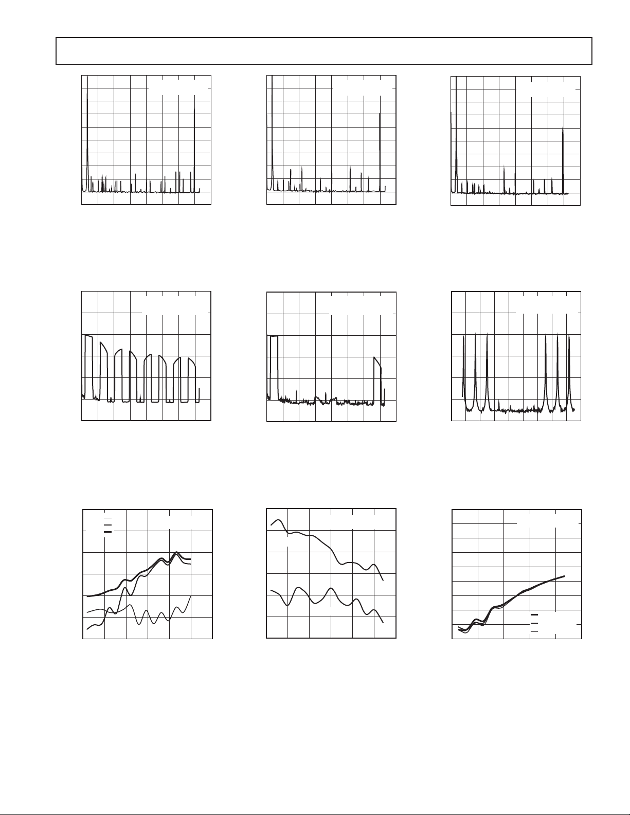
TPC 1. AD9862 Tx Output 6 MHz
Single Tone; CLKIN = 32 MHz;
0
Setting
f
= 32MSPS
DATA
1 INTERPOLATION
DLL 4
–20
–40
–60
140
0
–10
–20
–30
–40
–50
–60
–70
MAGNITUDE – dBm
–80
–90
–100
0
20 40
f
= 32MSPS
DATA
4 INTERPOLATION
80 100 110 120
60
FREQUENCY – MHz
TPC 2. AD9862 Tx Output 6 MHz
Single Tone; CLKIN = 64 MHz;
DLL 2 Setting
0
–20
–40
–60
f
= 32MSPS
DATA
4 INTERPOLATION
140
0
–10
–20
–30
–40
–50
–60
–70
MAGNITUDE – dBm
–80
–90
–100
0
20 40
FREQUENCY – MHz
f
DATA
4 INTERPOLATION
80 100 110 120
60
= 32MSPS
TPC 3. AD9862 Tx Output 6 MHz
Single Tone; CLKIN = 128 MHz;
DLL 1 Setting
0
–20
–40
–60
f
= 32MSPS
DATA
4 INTERPOLATION
140
–80
MAGNITUDE – dBm
–100
–120
0
20 40
60
80 100 110 120
FREQUENCY – MHz
140
TPC 4. TxDAC Generating an
OFDM Signal; CLKIN = 64 MHz,
DLL 2 Setting
–60
THD
2nd
3rd
–65
–70
–75
THD – dBc
–80
–85
–90
52035
10
f
= 64MSPS
DATA
2 INTERPOLATION
15 25 30
f
– MHz
OUT
TPC 7. TxDAC Harmonic
Distortion vs. f
OUT
–80
MAGNITUDE – dBm
–100
–120
0
20 40 60 80 100 110 120
FREQUENCY – MHz
140
TPC 5. TxDAC Generating an
OFDM Signal; CLKIN = 64 MHz,
DLL 2 Setting
74
73
72
71
SNR – dB
70
69
68
0
AD9862
5
f
= 64MSPS
DATA
2 INTERPOLATION
AD9860
10 15 25 30
FREQUENCY – MHz
20
TPC 8. Signal-to-Noise Ratio (SNR)
vs. f
OUT
–80
MAGNITUDE – dBm
–100
–120
7.92 7.94 7.96 7.98 8.00 8.02 8.04 8.06 8.08
7.90
FREQUENCY – MHz
TPC 6. Zoomed in Plot of Four
Notched Carriers of OFDM Signal;
CLKIN = 64 MHz, DLL 2 Setting
–50
–55
–60
–65
–70
–75
IMD – dBc
–80
–85
–90
–95
5
10 15 25 30
CARRIER FREQUENCY – MHz
f
= 64MSPS
DATA
2 INTERPOLATION
AV DD = 3.0V
AV DD = 3.3V
AV DD = 3.6V
20
TPC 9. Two Tone Intermodulation
vs. f
OUT1 (fOUT2
= f
+ 1 MHz)
OUT1
REV. 0
–9–
Page 10
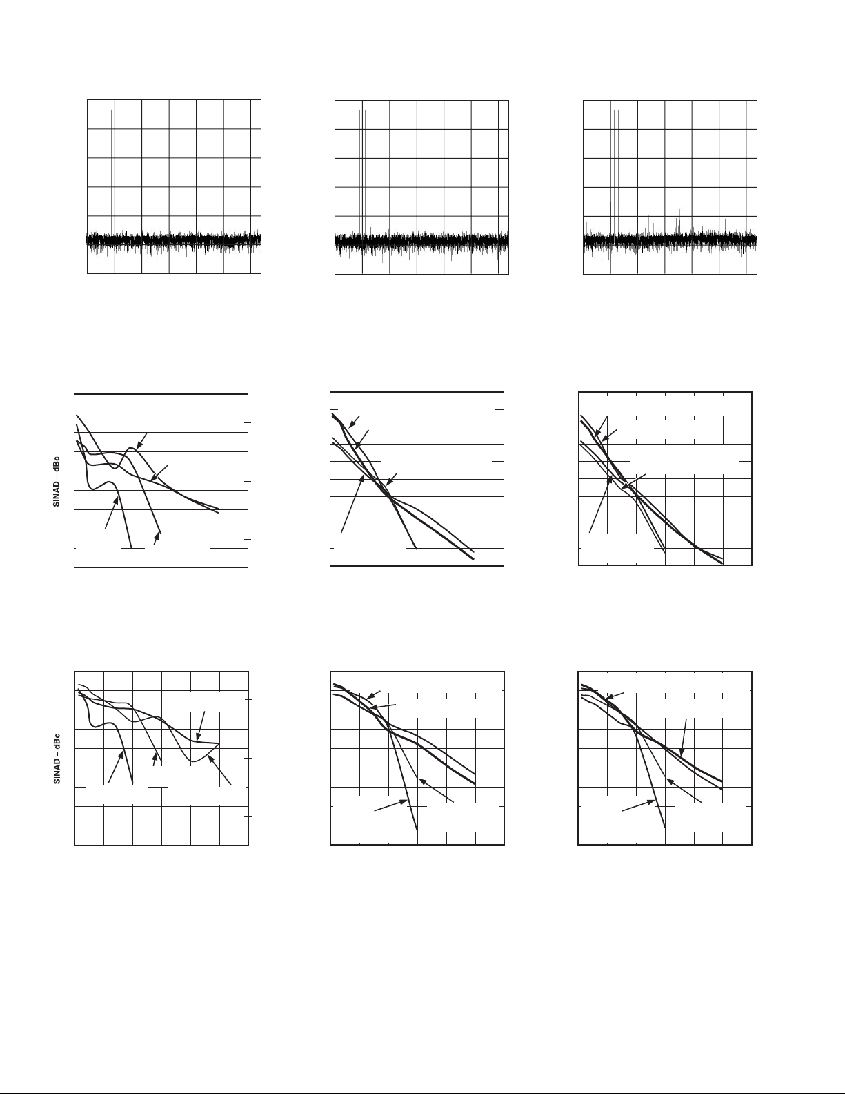
AD9860/AD9862
0
–20
–40
–60
–80
FFT MAGNITUDE – dBFS
–100
–120
5
0
10 15 25 30
FFT OUTPUT – MHz
20
TPC 10. ADC Dual Tone FFT with
Buffer Tones at 4.5 MHz and 5.5 MHz
68
66
64
62
60
58
56
54
52
50
0 20050
BUFFERED
2V INPUT,
1 GAIN
BUFFERED BYPASS
2V INPUT, 1 GAIN
BUFFERED BYPASS
1V INPUT, 2 GAIN
BUFFERED 1V
INPUT, 2 GAIN
150 250100
f
– MHz
IN
300
11.0
10.5
10.0
9.5
9.0
8.5
8.0
TPC 13. AD9862 Rx SINAD
at 64 MSPS
vs. f
IN
0
–20
–40
–60
–80
FFT MAGNITUDE – dBFS
–100
–120
0
10 15 25 30
5
FFT OUTPUT – MHz
20
TPC 11. ADC Dual Tone FFT without
Buffer Tones at 4.5 MHz and 5.5 MHz
70
LOW POWER MODE 1, BUFFER BYPASSED,
68
2V p-p INPUT, 1 RxPGA GAIN
66
64
62
60
58
SINAD – dBc
56
54
52
50
BUFFER BYPASSED, 2V p-p,
1 RxPGA GAIN
BUFFER ENABLED,
1V p-p INPUT,
2 RxPGA GAIN
0 20050
LOW POWER MODE 1, BUFFER
ENABLED, 1V p-p INPUT,
2 RxPGA GAIN
150 250100
f
– MHz
IN
300
TPC 14. AD9862 Rx SINAD
vs. f
at 32 MSPS
IN
0
–20
–40
–60
–80
FFT MAGNITUDE – dBFS
–100
–120
0
FFT OUTPUT – MHz
10 15 25 30
5
20
TPC 12. ADC Dual Tone FFT
(undersampling) without Buffer
Tones at 69.5 MHz and 70.5 MHz
70
LOW POWER MODE 2, BUFFER BYPASSED,
68
2V p-p INPUT, 1 RxPGA GAIN
66
64
62
60
58
SINAD – dBc
56
54
52
50
BUFFER BYPASSED, 2V p-p,
1 RxPGA GAIN
BUFFER ENABLED,
1V p-p INPUT,
2 RxPGA GAIN
0 20050
LOW POWER MODE 2, BUFFER
ENABLED, 1V p-p INPUT,
2 RxPGA GAIN
150 250100
f
– MHz
IN
TPC 15. AD9862 Rx SINAD
vs. f
at 16 MSPS
IN
300
62
60
58
56
54
52
50
48
46
44
0 20050
BUFFERED 2V
INPUT, 1 GAIN
BUFFERED BYPASS
1V INPUT, 2 GAIN
BUFFERED 1V
INPUT, 2 GAIN
BUFFERED BYPASS
2V INPUT, 1 GAIN
150 250100
f
– MHz
IN
TPC 16. AD9860 Rx SINAD
at 64 MSPS
vs. f
IN
300
10.0
9.5
9.0
8.5
8.0
7.5
7.0
62
LOW POWER MODE 1, BUFFER BYPASSED,
2V p-p INPUT, 1 RxPGA GAIN
60
58
56
54
52
SINAD – dBc
50
LOW POWER
48
MODE 1,
BUFFER ENABLED,
46
1V p-p INPUT,
2 RxPGA GAIN
44
0 20050
BUFFER BYPASSED, 2V p-p,
1 RxPGA GAIN
BUFFER ENABLED,
1V p-p INPUT,
2 RxPGA GAIN
150 250100
f
– MHz
IN
TPC 17. AD9860 Rx SINAD
at 32 MSPS
vs. f
IN
300
62
LOW POWER MODE 2, BUFFER BYPASSED,
2V p-p INPUT, 1 RxPGA GAIN
60
58
56
54
52
SINAD – dBc
50
LOW POWER
48
MODE 2,
BUFFER ENABLED,
46
1V p-p INPUT,
2 RxPGA GAIN
44
0 20050
BUFFER BYPASSED, 2V p-p,
1 RxPGA GAIN
BUFFER ENABLED,
1V p-p INPUT,
2 RxPGA GAIN
150 250100
f
– MHz
IN
TPC 18. AD9860 Rx SINAD
at 16 MSPS
vs. f
IN
300
REV. 0–10–
Page 11

AD9860/AD9862
–50
–55
–60
–65
–70
–75
–80
THD – dBc
–85
–90
–95
–100
BUFFERED BYPASS
2V INPUT, 1 GAIN
BUFFERED 2V
INPUT, 1 GAIN
BUFFERED 1V
INPUT, 2 GAIN
0 10010 1000
INPUT FREQUENCY – MHz
BUFFERED BYPASS
1V INPUT, 2 GAIN
TPC 19. Rx THD vs. fIN,
F
= 64 MSPS
ADC
–50
–55
–60
–65
–70
–75
–80
SFDR – dBc
–85
–90
–95
–100
0
BUFFERED BYPASS
1V INPUT, 2 GAIN
BUFFERED BYPASS
2V INPUT, 1 GAIN
BUFFERED 2V
INPUT, 1 GAIN
10 1000
INPUT FREQUENCY – MHz
BUFFERED 1V
INPUT, 2 GAIN
100
TPC 22. Rx SFDR @ 64 MSPS
–50
AD9860 LOW POWER
MODE 1, BUFFER
–55
ENABLED,
1V p-p INPUT,
2 RxPGA GAIN
–60
–65
–70
THD – dBc
–75
–80
–85
–90
0 20050
AD9860 LOW POWER MODE 1,
BUFFER BYPASSED, 2V p-p INPUT,
1 RxPGA GAIN
AD9862 LOW POWER MODE 1,
BUFFER BYPASSED, 2V p-p INPUT,
1 RxPGA GAIN
AD9862 LOW POWER
150 250100
fIN – MHz
MODE 1, BUFFER
ENABLED
1V p-p INPUT,
2 RxPGA GAIN
TPC 20. Rx THD vs. fIN,
= 32 MSPS
F
ADC
–50
AD9862 LOW POWER MODE 1,
BUFFER
ENABLED
–55
INPUT, 2 RxPGA GAIN
AD9860
–60
LOW POWER MODE 1,
BUFFER ENABLED,
–65
1V p-p INPUT,
2 RxPGA GAIN
–70
–75
SFDR – dBc
–80
–85
–90
–95
0 20050
AD9862 LOW POWER MODE 1,
BUFFER BYPASSED, 2V p-p INPUT,
1 RxPGA GAIN
, 1V p-p
BUFFER BYPASSED,
150 250100
f
– MHz
IN
LOW POWER
2V p-p INPUT,
1 RxPGA GAIN
TPC 23. Rx SFDR @ 32 MSPS
AD9860
MODE 1,
300
300
–50
AD9860 LOW POWER
MODE 2, BUFFER
,
–55
ENABLED,
1V p-p INPUT,
2 RxPGA GAIN
–60
–65
–70
THD – dBc
–75
–80
–85
–90
0 20050
AD9860 LOW POWER MODE 2,
BUFFER BYPASSED, 2Vp-p INPUT,
1 RxPGA GAIN
AD9862 LOW POWER MODE 2,
BUFFER BYPASSED, 2V p-p INPUT,
1 RxPGA GAIN
150 250100
fIN – MHz
AD9862
LOW POWER
MODE 2,
BUFFER
ENABLED
1V p-p INPUT,
2 RxPGA GAIN
,
300
TPC 21. Rx THD vs. fIN,
= 16 MSPS
F
ADC
–50
AD9860 LOW POWER MODE 2,
BUFFER BYPASSED, 1V p-p
–55
INPUT, 2 RxPGA GAIN
AD9860
–60
LOW POWER MODE 2,
BUFFER ENABLED,
–65
1V p-p INPUT,
2 RxPGA GAIN
–70
–75
SFDR – dBc
–80
–85
–90
–95
0 20050
AD9862 LOW POWER MODE 2,
BUFFER
2 RxPGA GAIN
AD9862 LOW POWER
MODE 2, BUFFER BYPASSED,
2V p-p INPUT, 1 RxPGA GAIN
ENABLED
, 1V p-p INPUT,
150 250100
f
– MHz
IN
300
TPC 24. Rx SFDR @ 16 MSPS
1
0
–1
–2
–3
–4
NO BUFF 2V 1
RELATIVE ATTENUATION – dB
–5
BUFF 1V 2
BUFF 2V 1
–6
1
10
INPUT FREQUENCY – MHz
100 1000
TPC 25. Rx Input Attenuation
280
270
260
250
240
230
220
210
INPUT IMPEDANCE –
200
190
180
0
20 40 80 100
f
IN
TPC 26. Rx Input Buffer
Impedance vs. f
– MHz
800
f
ADC
30 5020
NOMINAL
– MSPS
70
60
700
600
500
400
300
200
Rx ANALOG POWER – mW
100
60
32MSPS LP MODE
16MSPS LP MODE
0
04010
TPC 27. Rx Analog Power
IN
Consumption
REV. 0
–11–
Page 12

AD9860/AD9862
REGISTER MAP (0x00–0x3F)
1
Register Name Address2Bit 7 Bit 6 Bit 5 Bit 4 Bit 3 Bit 2 Bit 1 Bit 0
General 0 SDIO BiDir LSB First Soft Reset
Rx Power Down 1 V
Rx A2Byp Buffer A RxPGA A
Rx B3Byp Buffer B RxPGA B
Rx Misc 4
Rx I/F 5 Three State Rx Retime Twos Inv RxSync Mux Out
Rx Digital 6 2 Channel Keep –ve Hilbert Decimate
RSV 7
Tx Power Down 8 Alt Timing TxOff Enable Tx Digital Tx Analog Power Down [2:0]
RSV9 Reserved for Future Use
Tx A Offset 10
Tx A Offset 11 DAC A Offset [9:2]
Tx B Offset 12
Tx B Offset 13 DAC B Offset [9:2]
Tx A Gain 14
Tx B Gain 15 DAC B Coarse Gain DAC B Fine Gain
Tx PGA Gain 16
Tx Misc 17 Slave Enable Tx PGA Fast
Tx I/F 18 Tx Retime Q/I Order Inv TxSync Twos Inverse 2 Edges Interleaved
Tx Digital 19 2 Data Paths Keep –ve Hilbert Interpolation Control
Tx Modulator 20 Neg. Fine Tune Fine Mode Real Mix Neg. Coarse Tune Coarse Modulation
NCO Tuning
Word
NCO Tuning
Word
NCO Tuning
Word
DLL 24 Reserved Input Control ADC Div 2 DLL Multiplier DLL DLL
CLKOUT 25 CLKOUT2 Divide Factor Inv2 Dis2 Inv1 Dis1
Aux ADC A2 26
Aux ADC A2 27 Aux ADC A2 Data [9:2]
Aux ADC A1 28
Aux ADC A1 29 Aux ADC A1 Data [9:2]
Aux ADC B2 30
Aux ADC B2 31 Aux ADC B2 Data [9:2]
Aux ADC B1 32
Aux ADC B1 33 Aux ADC B1 Data [9:2]
Aux ADC Control 3 4 Aux SPI SelBnot A Refsel B Select B Start B Refsel A Select A Start A
Aux ADC Clock 35 CLK/4
Aux DAC A 36
Aux DAC B 37
Aux DAC C
Aux DAC 39 Slave Enable Update C Update B Update A
Update Aux DAC 40 Power Down C Power Down B Power Down A
DAC Control 41 Inv C Inv B Inv A
SigDelt 42 Sigma-Delta Control Word [3:0] Flag
SigDelt 43 Sigma-Delta Control Word [11:4]
ADC Low Power 49, 50
RSV 44–62
NOTES
1
When writing to a register with unassigned register bit(s), a logic low must be written to the unassigned bit(s). By default, after power up or RESET, all registers
are set low, except for the bits in the shaded boxes, which are set high.
2
Decimal
21 FTW [7:0]
22 FTW [15:8]
23 FTW [23:16]
38
63 Chip Rev ID
(diff) V
REF
DAC A Offset [1:0] DAC A Offset
DAC B Offset [1:0] DAC B Offset
DAC A Coarse Gain DAC A Fine Gain
Aux ADC A2 Data [1:0]
Aux ADC A1 Data [1:0]
Aux ADC B2 Data [1:0]
Aux ADC B1 Data [1:0]
REF
Clock Power Down FAST
Low Power Register for Rx Path Operation below 32 MSPS
Rx Digital Rx Channel B Rx Channel A Buffer B Buffer A All Rx
Reserved for Future Use
Mode
Tx PGA Gain
Aux DAC A
Aux DAC B
Aux DAC C
Reserved for Future Use
HS Duty Cycle
Complement
Complement Sample
Shared Ref Clk Duty
Direction
Direction
Purpose
SPI Setup
Receive
Path
Setup
Transmit
Path
Setup
NCO
Setup
Clock
Setup
Auxiliary
ADC Data
and Setup
Auxiliary
DAC Data
and Setup
SigmaDelta Data
and Setup
Rx Low
Power
Reserved
Chip ID
REV. 0–12–
Page 13

AD9860/AD9862
REGISTER BIT DEFINITIONS
REGISTER 0: GENERAL
BIT 7: SDIO BiDir (Bidirectional)
Default setting is low, which indicates SPI serial port uses dedicated input and output lines (i.e., 4-wire interface), SDIO and
SDO Pins, respectively. Setting this bit high configures the
serial port to use the SDIO Pin as a bidirectional data pin.
BIT 6: LSB First
Default setting is low, which indicates MSB first SPI Port Access
Mode. Setting this bit high configures the SPI port access to
LSB first mode.
BIT 5: Soft Reset
Writing a high to this register resets all the registers to their
default values and forces the DLL to relock to the input clock.
The Soft Reset Bit is a one shot register and is cleared immediately
after the register write is completed.
REGISTER 1: Rx PWRDWN
BIT 7: V
, diff (Power-Down)
REF
Setting this bit high will power down the ADC’s differential
references (i.e., REFT and REFB).
BIT 6: V
(Power-Down)
REF
Setting this register bit high will power down the ADC reference
circuit (i.e., V
BIT 5: Rx Digital (Power-Down)
REF
).
Setting this bit high will power down the digital section of the
receive path of the chip. Typically, any unused digital blocks are
automatically powered down.
BIT 4/3: Rx Channel B/Rx Channel A (Power-Down)
Either ADC or both ADCs can be powered down by setting the
appropriate register bit high. The entire Rx channel is powered
down, including the differential references, input buffer, and the
internal digital block. The bandgap reference remains active for
quick recovery.
BIT 2/1: Buffer B/Buffer A (Power-Down)
Setting either of these bits high will power down the input buffer
circuits for the respective channel. The input buffer should be
powered down when bypassed. By default, these bits are low and
the input buffers are enabled.
BIT 0: All Rx (Power-Down)
Setting this bit high powers down all circuits related to the
receive path.
REGISTER 2/3: Rx A/Rx B
BIT 7: Bypass Buffer A/Bypass Buffer B
Setting either of these bits high will bypass the respective input buffer circuit. When the buffer is bypassed, the input signal is routed
directly to the switched capacitor SHA input of the RxPGA. When
operating with buffer bypassed, it should be powered down.
BIT 0–4: RxPGA A/RxPGA B
These 5-bit straight binary registers (Bit 0 is the LSB, Bit 4 is the
MSB) provide control for the programmable gain amplifiers in
the dual receive paths. A 0 dB to 20 dB gain range is accomplished through a switched capacitor network with fast settling
of a few clock cycles. The step size is approximately 1 dB. The
register default setting is minimum gain or hex00. The maximum
setting for these registers is hex14.
REGISTER 4: Rx MISC
BIT 2: HS (High Speed) Duty Cycle
Setting this bit high optimizes duty cycle of the internal ADC
sampling clock. It is recommended that this bit be set high in
REV. 0
–13–
high speed applications when clock duty cycle affects noise and
distortion performance the most. This bit should be set high in
conjunction with Clk Dut Enable register bit.
BIT 1: Shared Ref
Setting this bit high forces the dual receive ADCs into a mode
to share their differential references to provide superior gain
matching. When this option is enabled, the REFT of Channel A
and Channel B should be connected together off-chip and the
REFB of both channels should be connected.
BIT 0: Clk Duty
Setting this bit high enables an on-chip duty cycle stabilizer (DCS)
circuit to generate the internal clock for the Rx block. This option
is useful for adjusting for high speed input clocks with skewed
duty cycle. The DCS Mode can be used with ADC sampling
frequencies over 40 MHz.
REGISTER 5: Rx I/F (INTERFACE)
BIT 4: Three-state
Setting this bit high will force both Rx data output buses, including
the RxSYNC Pin, into a three-state mode.
BIT 3: Rx Retime
The Rx path can use either of the clock outputs, CLKOUT1 or
CLKOUT2, to latch the Rx output data. Since CLKOUT1 and
CLKOUT2 have slight phase offsets, this provides some timing
flexibility with the interface. By default, this bit is low and the
Rx output latches use CLKOUT1. Setting this bit will force the
Rx output latches to use CLKOUT2.
BIT 2: Twos Complement
Default data format for the Rx data is straight binary. Setting this
bit high will generate two’s complement data.
BIT 1: Inv RxSync
When the receive data is multiplexed onto one data port (i.e., Mux
Mode Enabled), the RxSYNC Pin can be used to decode which
channel generated the current output data at the active port.
Default condition is that RxSYNC is high when Channel A is at
the output and is low when Channel B is at the output. Setting
this bit high reverses this synchronization.
BIT 0: Mux Out
Setting this bit high enables the Rx Mux Mode. Default setting
is low, which is Dual Port Mode, (i.e., non Rx Mux Mode). When in
Rx Mux Mode, both Rx channels share the same output data bus,
pins D0A to D9A (for AD9860) or D0A to D11A (for AD9862).
The other Rx output bus (pins D0B to D9B or D0B to D11B)
outputs a low logic.
REGISTER 6: Rx Digital
BIT 3: 2 Channel
Setting this bit low disables the Rx B output data port (pins D0B
to D9B or D11B), forcing the output pins to zero. By default, the
bit is high and both data paths are active.
BIT 2: Keep –ve
This bit selects whether the receive Hilbert filter will filter positive
or negative frequencies, assuming the filter is enabled. By default
this bit is low, which passes positive frequencies. Setting this bit
high will configure the filter to pass negative frequencies.
BIT 1: Hilbert
This bit enables or disables the Hilbert filter in the receive path.
By default, this bit is low, which disables the receive Hilbert filter.
Setting this bit high enables the receive Hilbert filter.
BIT 0: Decimate
This register enables or disables the decimation filters. By default,
the register setting is low and the decimation filter is disabled.
Page 14

AD9860/AD9862
Setting this bit high enables the decimation filters and decimates
the receive data by two.
REGISTER 8: Tx PWRDWN
BIT 5: Alt Timing Mode
The timing section in the data sheet describes two timing modes,
the “Normal Operation” and the “Alternate Operation” modes.
At power up, the default configuration is established from the
logic level of the Mode/TxBlank pin. If Mode/TxBlank is logic
low, the Normal Operation mode is the default; if the Mode/
TxBlank pin is held at a logic high, the Alternative Operation
mode is configured at power-up (the DLL is forced to multiply
by 4 at power-up by default in this mode). After power up, the
operation mode can be configured so that the Mode/TxBlank pin
can be used for other functions. To allow this, set this bit high.
BIT 4: TxOff Enable
By default, the Mode/TxBlank pin is not used for any transmit
synchronization. The Mode/TxBlank pin input can be used to
serve two functions, blanking the DAC outputs and slaving the
TxPGA gain control. When this bit is set high, a logic high on the
Mode/TxBlank pin forces the Tx digital block to stop clocking. In
this mode, the Tx outputs will be static, holding their last update
values. To slave the TxPGA gain control to the Mode/TxBlank
pin input, register Slave Enable (Register 17, Bit 1) needs to also
be programmed. See that register for more information.
BIT 3: Tx Digital (Power-Down)
By default this bit is low, enabling the transmit path digital to
operate as programmed through other registers. By setting this
bit high, the digital blocks are not clocked to reduce power consumption. When enabled, the Tx outputs will be static, holding
their last update values.
BIT 0-2: Tx Analog (Power-Down)
Three options are available to reduce analog power consumption
for the Tx channels. The first two options disable the analog output
from Tx channel A or B independently, and the third option
disables the output of both channels and reduces the power
consumption of some of the additional analog support circuitry
for maximum power savings. With all three options, the DAC bias
current is not powered down so recovery times are fast (typically
a few clock cycles). The list below explains the different modes
and settings used to configure them.
Tx Analog
Power-Down
Power-Down Option Bits Setting [2:0]
Power-Down Tx B Channel Analog Output [1 0 0]
Power-Down Tx A Channel Analog Output [0 1 0]
Power-Down Tx A and Tx B Analog Outputs [1 1 1]
REGISTER 10/11/12/13: DAC OFFSET A/B
DAC A/DAC B Offset
These 10-bit, twos complement registers control a dc current
offset that is combined with the Tx A or Tx B output signal. An
offset current of up to ±12% I
(2.4 mA for a 20 mA full-
OUTFS
scale output) can be applied to either differential pin on each
channel. The offset current can be used to compensate for offsets
that are present in an external mixer stage, reducing LO leakage
at its output. Default setting is hex00, no offset current. The
offset current magnitude is set using the lower nine bits. Setting
the MSB high will add the offset current to the selected differential pin, while an MSB low setting will subtract the offset value.
DAC A/DAC B Offset Direction
This bit determines to which of the differential output pins for
the selected channel the offset current will be applied. Setting this
bit low will apply the offset to the negative differential pin. Setting
this bit high will apply the offset to the positive differential pin.
REGISTER 14/15: DAC GAIN A/B
BIT 6, 7: DAC A/DAC B Coarse Gain Control
These register bits will scale the full-scale output current (I
of either Tx channel independently. I
function of the R
resistor, the TxPGA setting, and the Coarse
SET
of the Tx channels is a
OUT
OUTFS
)
Gain Control setting.
MSB, LSB Tx Channel Current Scaling
10 or 11 Does not scale output current
01 Scales output current by 1/2
00 Scales output current by 1/11
BIT 5–0: DAC A/DAC B Fine Gain
The DAC output curve can be adjusted fractionally through the
Gain Trim Control. Gain trim of up to ±4% can be achieved on
each channel individually. The Gain Trim register bits are a twos
complement attention control word.
MSB, LSB
100000 Maximum positive gain adjustment
111111 Minimum positive gain adjustment
000000 No adjustment (default)
000001 Minimum negative gain adjustment
011111 Maximum negative gain adjustment
REGISTER 16: TxPGA GAIN
BIT 0–7: TxPGA Gain
This 8 bit, straight binary (Bit 0 is the LSB, Bit 7 is the MSB) register controls for the Tx programmable gain amplifier (TxPGA).
The TxPGA provides a 20 dB continuous gain range with 0.1 dB
steps (linear in dB) simultaneously to both Tx channels. By
default, this register setting is hex00.
MSB, LSB
000000 Minimum gain scaling –20 dB
111111 Maximum gain scaling 0 dB
REGISTER 17: Tx MISC
BIT 1: Slave Enable
The TxPGA Gain is controlled through register TxPGA Gain
setting and by default is updated immediately after the register
write. If this bit is set, the TxPGA Gain update is synchronized
with the rising edge of a signal applied to the Mode/TxBlank
pin. Setting TxOff enable in Register 8 is also required.
BIT 0: TxPGA Fast (Update Mode)
The TxPGA Fast bit controls the update speed of the TxPGA.
When Fast Update mode is enabled, the TxPGA provides fast gain
settling within a few clock cycles. Default setting for this bit
is low, which indicates Normal Update mode. Fast mode is
enabled when this bit is set high.
REGISTER 18: Tx IF (INTERFACE)
BIT 6: Tx Retime
The Tx path can use either of the clock outputs, CLKOUT1 or
CLKOUT2, to latch the Tx input data. Since CLKOUT1 and
CLKOUT2 have slight phase offsets, this provides some timing
flexibility with the interface. By default, this bit is high and the
Tx input latches use CLKOUT1. Setting this bit low will force
the Tx latches to use CLKOUT2.
REV. 0–14–
Page 15

AD9860/AD9862
BIT 5: Q/I Order
This register indicates the order of received complex transmit
data. By default this bit is low, representing I data preceding
Q data. Alternatively, if this bit is set high, the data format is
defined as Q data preceding I data.
BIT 4: Inv TxSync
This register identifies how the first and second data sets are
identified in a complex data set using the TxSYNC bit. By default
this bit is low, and TxSYNC low indicates the first data set is at
the Tx port; TxSYNC high indicates the second data set is at the
Tx port. Setting this bit high inverts the TxSYNC bit. TxSYNC
high indicates the first of the data set, and TxSYNC low indicates
the second of the data set.
BIT 3: Twos Complement
The default data format for Tx data is straight binary. Set this bit
high when providing twos complement Tx data.
BIT 2: Inverse Sample
By default, the transmit data is sampled on the rising edge of the
CLKOUT. Setting this bit high will change this, and the transmit
data will be sampled on the falling edge.
BIT 1: 2 Edges
If the CLKOUT rate is running at half the interleaved data rate,
both edges of the CLKOUT must latch transmit data. Setting
this bit high allows this clocking configuration.
BIT 0: Interleaved
By default, the AD9860/AD9862 powers up in single DAC
operation. If dual transmit data is to be used, the interleaved data
option needs to be enabled by setting this bit high.
REGISTER 19: Tx DIGITAL
BIT 4: 2 Data Paths
Setting this bit high enables both transmit digital paths. By default,
this bit is low and the transmit path utilizes only a single channel.
BIT 3: Keep –ve
This bit configures the Tx Hilbert filter for either positive or negative frequencies pass band, assuming it is enabled. By default
this bit is low, which selects the positive frequencies. Setting this
bit high will setup the Hilbert filter to pass negative frequencies.
BIT 2: Hilbert
This bit enables or disables the Hilbert filter in the transmit path.
By default, this bit is low, which disables the transmit Hilbert
filter. Setting this bit high enables the transmit Hilbert filter.
BIT 1,0: Interpolation Control
These register bits control the interpolation rate of the transmit
path. Default settings are both bits low, indicating that both interpolation filters are bypassed. The MSB and LSB are address D19,
Bits 1 and 0, respectively. Setting binary 01 provides an interpolation rate of 2; binary 10 provides an interpolation rate of 4.
REGISTER 20: Tx MODULATOR
BIT 5: Negative Fine Tune
When this bit is low (default), the Numerically Controlled Oscillator (NCO) provides positive shifts in frequency, assuming fine
modulation is enabled. Setting this bit high will use a negative
frequency shift in the Fine Complex Modulator.
BIT 4: Fine Mode
By default, the NCO and fine modulation stage are bypassed. Setting
this bit high will enable the use of the digital complex modulator,
enabling tuning with the NCO.
BIT 3: Real Mix Mode
This bit determines if the coarse modulation (controlled by register
Coarse Modulation, will perform a separate real mix on each
channel or a complex mix using the dual channel data. By default,
this bit is set low and a complex mix will be performed. Setting
this bit high will enable the Real Mix mode. Note, the Fine
Modulator Block only performs complex mixing.
BIT 2: Negative Coarse Tune
When this bit is low (default), the coarse modulator provides
positive shifts in frequency. Setting this bit high will shift the coarse
modulator processed data negative in frequency.
BIT 1,0: Coarse Modulation
These bits control what coarse modulation processing will be
performed on the transmit data. A setting of binary 00 (default)
will bypass the modulation block, a setting of binary 01 will shift
the transmit data by f
the transmit data by f
REGISTER 21/22/23: NCO TUNING WORD
FTW [23:0]
/4, and a setting of binary 10 will shift
DAC
/8.
DAC
These three registers set the 24-bit frequency tuning word (FTW)
for the NCO in the fine modulator stage of the Tx path. The
NCO full-scale tuning word is straight binary and produces
a frequency equivalent to f
REGISTER 24: DLL
BIT 6: Input Clock Control
DAC
/4 with a resolution of f
DAC
/226.
This bit defines what type of clock will be driving the AD9860/
AD9862. The default state is low, which allows either crystal connected to OSC1 and OSC2 or single-ended reference clock driving
OSC1 to drive the internal timing circuits. If a crystal will not be
used, the internal oscillator should be disabled after power-up
by setting this bit high.
BIT 5: ADC Div2
By default, the ADC is driven directly by the input clock in Normal
Timing Operation mode or the DLL output in the Alternative
Timing Operation mode. Setting this bit high will clock the ADC
at one half the previous clock rate. This is described further in
the timing section.
BIT 4,3: DLL Multiplier
These bits control the DLL multiplication factor. A setting of
binary 00 will bypass the DLL, a setting of binary 01 will multiply
the input clock by 2, and a setting of binary 10 will multiply the
input clock by 4. Default mode is defined by Mode/TxBlank
logic level at power-up or RESET, which configures either Normal
Operation Timing mode or Alternative Timing mode. In Alternative Timing mode, the DLL will lock to 4 multiplication
factor (the DLL FAST register remains low by default). If the
Mode/TxBlank pin is low, by default the DLL will be bypassed
and a 1 clock is used internally.
BIT 2: DLL Power-Down
Setting this register bit high forces the CLK IN multiplier to a
power-down state. This mode can be used to conserve power or
to bypass the internal DLL. To operate the AD9860/AD9862
when the DLL is bypassed, an external clock equal to the fastest
on-chip clock is supplied to the OSC pin(s).
BIT 0: DLL FAST
The DLL can be used to generate output frequencies between
32 MHz to 128 MHz. Because of the large range of locking frequencies allowed, the DLL is separated into two output frequency
ranges, a “slow” range between 32 MHz to 64 MHz and a “fast”
range starting at frequencies above 64 MHz to 128 MHz. By
REV. 0
–15–
Page 16

AD9860/AD9862
default, this bit is low, setting up the DLL in “slow” mode. This
bit must be set high for DLL output frequencies over 64 MHz.
REGISTER 25: CLKOUT
BIT 7, 6: CLKOUT2 Divide Factor
These bits control what rate the CLKOUT2 Pin will operate at
relative to the DLL output rate. The DLL output rate can be
output directly or divided by 2, 4, or 8. Bit 7 is the MSB and
Bit 6 is the LSB.
MSB, LSB Relative CLKOUT2 Frequency
00 (Default) Equals DLL output rate
01 Equals DLL output rate divided by 2
10 Equals DLL output rate divided by 4
11 Equals DLL output rate divided by 8
BIT 5, 1: Inv 2/Inv 1
The output clocks from CLKOUT1 and CLKOUT2 can be
inverted by setting the appropriate one of these bits high.
BIT 4, 0: Dis 2/Dis 1
The output clocks from CLKOUT1 and CLKOUT2 can be
disabled and a logic low output is forced by setting the appropriate one of these bits high.
REGISTER 26–33: AUXILIARY ADC A2/A1/B2/B1
AUX ADC A2, A1, B2, B1 Data
These registers are read only registers that are used for read
back of the 10-bit auxiliary ADC. The 10 bits are broken into a
two registers, one containing the upper eight bits and the other
containing the lower two bits.
REGISTER 34: AUX ADC CONTROL
BIT 7: Aux SPI (Enable)
One of the Auxiliary ADCs can be controlled through an dedicated Auxiliary Serial Port. Setting this bit high enables this mode.
BIT 6: Sel BnotA
If the auxiliary Serial port is used, this bit selects which Auxiliary
ADC, A or B, will be using the dedicated Auxiliary Serial port.
The Auxiliary Serial port by default (low setting) controls Auxiliary ADC A. Setting this bit high will allow the Auxiliary Serial
Port to control Auxiliary ADC B.
BIT 5, 2: Refsel B/A
By default, the auxiliary ADCs use an external reference applied to
the AUX_REF pin. This voltage will act as the full-scale reference
for the selected auxiliary ADC. Either auxiliary ADC can use an
internally generated reference, which is a buffered version of the
analog supply voltage. To enable use of the internal reference for
either of the auxiliary ADCs, the respective Refsel register should
be set high.
BIT 4, 1: Select B/A
These bits select which of the two inputs will be connected to the
respective auxiliary ADC. By default (setting low), the AUX_ADC_A2
pin is connected to Auxiliary ADC A and AUX_ADC_B2 pin is
connected to Auxiliary ADC B. Setting the respective bit high
will connect the AUX_ADC_A1 pin to Auxiliary ADC A and/or
AUX_ADC_B1 pin to Auxiliary ADC B.
BIT 3, 0: Start B/A
Setting a high bit to either of these registers initiates a conversion
of the respective auxiliary ADC, A or B. The register bit always
reads back a low.
REGISTER 35: AUX ADC CLOCK
BIT 0: CLK/4
By default (setting low), the auxiliary ADCs are run at the receive
ADC conversion rate divided by 2. Setting this bit high will run
the Auxiliary ADCs with a clock that is 1/4 of the receive ADC
conversion rate. The conversion rate of the auxiliary ADCs
should be less than 20 MHz.
REGISTER 36, 37, 38: AUX DAC A/B/C
Auxiliary DAC A, B, and C Output Control Word
Three 8-bit, straight binary words are used to control the output
of three on-chip auxiliary DACs. The auxiliary DAC output
changes take effect immediately after any of the serial write is
completed. The DAC output control words have default values
of 0. The smaller programmed output controlled words correspond to lower DAC output levels.
REGISTER 39: AUX DAC UPDATE
BIT 7: Slave Enable
A low setting (default) updates the auxiliary DACs after the respective register is written to. To synchronize the auxiliary DAC outputs
to each other, a slave mode can be enabled by setting this bit
high and then setting a high to the appropriate update registers.
BIT 2/1/0: Update C, B, and A
Setting a high bit to any of these registers initiates an update of the
respective Auxiliary DAC, A, B, or C, when Slave mode is enabled
using the Slave Enable register. The register bit is a one shot
and always reads back a low. Note: be sure to keep the Slave Enable
bit high when using the auxiliary DAC synchronization option.
REGISTER 40: AUX DAC POWER-DOWN
BIT 2/1/0: Power Down C, B, and A
Setting any of these bits high will power down the appropriate
auxiliary DAC. By default, these bits are low and the auxiliary
DACs are enabled.
REGISTER 41: AUX DAC CONTROL
BIT 4, 2, 0: Inv C, B, and A
Setting any of these bits high will invert the appropriate Auxiliary
DAC control word setting. By default, these bits are low and the
output control word is decoded as noninverted, straight binary.
REGISTER 42/43: SIGDELT (SIGMA-DELTA)
Sigma-Delta Output Control Word
A 12-bit straight binary word is used to control the output of an
on-chip sigma-delta converter. The sigma-delta output changes
take effect immediately after any serial write is completed. The
sigma-delta output control words have default values of 0. The
smaller programmed output controlled words correspond to lower
integrated sigma-delta output levels.
REGISTER 49,50 : RX LOW POWER MODE
Setting these bits will scale down the bias current to the ADC
analog block when the device is operated at lower speeds. By
default, these bits are low and the bias is at a nominal setting.
For ADC operation at or below 32 MSPS, Register 49 can be set
to 0x03 and Register 50 can be set to 0xEC; this will reduce Rx
AVDD power consumption by about 30% relative to nominal.
For ADC operation at or below 16 MSPS, Register 49 can be set
to 0x03 and Register 50 can be set to 0x9E; this will reduce Rx
AVDD power consumption by about 60% relative to nominal.
REGISTER 63: CHIP ID
BIT 7–0: Rev ID
This read only register indicates the revision of the AD9860/AD9862.
Reserved Registers
Reserved registers are held for future development and should
never be written to.
REV. 0–16–
Page 17

AD9860/AD9862
Blank Registers
Blank registers, i.e., the registers with 0 settings and no indicated
function, are placeholders used throughout the register map for
spacing the AD9860/AD9862 control bits in a logic fashion and,
potentially can be used for future development. A low should
always be written to these registers if a write needs to take place.
SERIAL PORT INTERFACE
The Serial Port Interface (SPI) is used to write to and read from
the AD9860/AD9862 internal programmable registers. The serial
interface uses four pins: SEN, SCLK, SDIO, and SDO by default.
SEN is a serial port enable pin, SCLK is the serial clock pin,
SDIO is a bidirectional data line and SDO is a serial output pin.
SEN is an active low control gating read and write cycles. When
SEN is high, SDO and SDIO are three-stated.
SCLK is used to synchronize SPI read and writes at a maximum
bit rate of 16 MHz. Input data is registered on the rising edge and
output data transitions on the falling edge. During write operations, the registers are updated after the 16th rising clock edge
(and 24th rising clock edge for the dual byte case). Incomplete
write operations are ignored.
SDIO is an input only by default. Optionally, a 3-pin interface may
be configured using the SDIO for both input and output operations and three-stating the SDO pin (see SDIO BiDir register).
t
t
HI
t
LO
CLK
SEN
t
t
S
DH
t
DS
SDO is a serial output pin used for read back operations in 4-wire mode
and is three-stated when SDIO is configured for bidirectional operation.
Instruction Header
Each SPI read or write consists of an instruction header and
data. The instruction header is made up of an 8-bit word and is
used to set up the register data transfer. The 8-bit word consists
of a read/not write bit, R/nW (the MSB), followed by a double/
not single bit (2/n1) and the 6-bit register address.
Write Operations
The SPI write operation uses the instruction header to configure
a one or two register write using the 2/n1 bit. The instruction
byte followed by the register data, is written serially into the
device through the SDIO pin on rising edges of the interface
clock at SCLK. The data can be transferred MSB first or LSB first
depending on the setting of the LSB First register.
Figure 1 includes a few examples of writing data into the device.
Figure 1a shows a write using 1 Byte and MSB First mode set;
Figure 1b shows an MSB first, 2 Byte write; and Figure 1c
shows an LSB first, 2 Byte write. Note the differences between
LSB and MSB First modes: instruction header and data are
reversed, and in 2 Byte writes, the first data byte is written to
the address in the header, N and the second data byte is written
to the n–1 address. In LSB First mode, the first data byte is still
written to the address in the instruction header, but the second
data byte is written to the N+1 address.
t
H
SCLK
SDIO
SEN
SCLK
SDIO
SEN
SCLK
SDIO
DON’T CARE
DON’T CARE
DON’T CARE
DON’T CARE
R/nW 2/n1 A5 A4 A3 A2 A1 A0 D7 D6 D5 D4 D3 D2 D1 D0
REGISTER DATAINSTRUCTION HEADER
t
2/n1
DH
t
DS
t
DH
t
DS
t
S
R/nW
t
S
A0 A1 A2 A3 A4 A5
t
t
LO
CLK
t
HI
REGISTER (N–1) DATAREGISTER (N) DATAINSTRUCTION HEADER (REGISTER N)
t
t
LO
CLK
t
HI
2/n1 R/nW
D0 D1 D2 D3 D4 D5 D6 D7 D0 D1 D2 D3 D4 D5 D6 D7
DON’T CARE
t
H
DON’T CARE
D0D1D2D3D4D5D6D7D0D1D2D3D4D5D6D7A0A1A2A3A4A5
t
H
DON’T CARE
DON’T CARE
DON’T CARE
DON’T CARE
REV. 0
REGISTER (N+1) DATAREGISTER (N) DATAINSTRUCTION HEADER (REGISTER N)
Figure 1. SPI Write Examples a. (top) 1 Byte, MSB First Mode; b. (middle) 2 Byte, MSB First Mode;
c. (bottom) 2 Byte, LSB First Mode
–17–
Page 18

AD9860/AD9862
SEN
SCLK
SDIO
SDO
SEN
SCLK
SDIO
DON’T CARE
DON’T CARE
DON’T CARE
DON’T CARE
t
t
S
t
S
R/nW
R/nW
DH
t
DS
2/n1 A5 A4 A3 A2 A1 A0
INSTRUCTION HEADER (REGISTER N)
DON’T CARE
t
DH
t
DS
2/n1 A5 A4 A3 A2 A1 A0 D7 D6 D5 D4 D3 D2 D1 D0
INSTRUCTION HEADER
t
LO
t
HI
t
LO
t
HI
t
t
CLK
CLK
t
DV
DON’T CARE
D7 D6 D5 D4 D3 D2 D1 D0
OUTPUT REGISTER DATA
t
DV
OUTPUT REGISTER DATA
t
H
DON’T CARE
t
H
DON’T CARE
DON’T CARE
DON’T CARE
t
LO
t
HI
2/n1
t
CLK
R/nW
SEN
SCLK
SDIO
SDO
DON’T CARE
DON’T CARE
t
t
S
A0 A1 A2 A3 A4 A5
DH
t
DS
INSTRUCTION HEADER
DON’T CARE
Figure 2. SPI Read Examples a. (top) 4-Wire Interface, MSB first; b. (middle) 3-Wire Interface, MSB first;
c. (bottom) 4-Wire Interface, LSB first
Read Operation
The read back of registers is a single data byte operation. The
readback can be configured to use three pins or four pins and can
be formatted as MSB first or LSB first. The instruction header
is written to the device either MSB or LSB first (depending on
the mode) followed by the 8-bit output data (appropriately MSB
or LSB justified). By default, the output data is sent to the dedicated
output pin (SDO). 3-wire operation can be configured by setting the SDIO BiDir register. In 3-wire mode, the SDIO pin
will become an output pin after receiving the 8-bit instruction
header with a read back request.
Figure 2a shows an MSB first, 4-pin SPI read; Figure 2b shows an
MSB first, 3-pin read; and Figure 2c shows an LSB first, 4-pin read.
SYSTEM BLOCK DESCRIPTION
The AD9860/AD9862 integrates transmit and receive paths with
digital signal processing blocks and auxiliary features. The auxiliary
t
t
DV
DON’T CARE
D0 D1 D2 D3 D4 D5 D6 D7
OUTPUT REGISTER DATA
H
DON’T CARE
DON’T CARE
features include two auxiliary ADCs, a programmable sigma-delta
output, three auxiliary DACs, integrated clock circuitry to generate
all internal clocks, and buffered output clocks from a single input
reference.
The AD9860/AD9862 system functionality is described in the
following four sections: the Transmit Block, Receive Block, Timing
Generation Block, and the Auxiliary Function Block. The following
sections provide a brief description of the blocks and applications
for the four sections.
TRANSMIT SECTION COMPONENTS
The transmit block (Tx) accepts and can process real or complex
data. The Tx interface is configurable for a variety of data formats
and has special processing options such as interpolation and Hilbert
filters. A detailed block diagram of the AD9860/AD9862 transmit
path is shown in Figure 3. The transmit block diagram is broken
into these stages: DAC (Block A), Coarse Modulation (Block B),
REV. 0–18–
Page 19

IOUT+A
IOUT–A
IOUT+B
IOUT–B
BLOCK A BLOCK B BLOCK C BLOCK D BLOCK E
BYPASSABLE
LOW-PASS
INTERPOLATION
FILTER
BYPASSABLE
DIGITAL
QUADRATURE
MIXER
DDS
I
Q
PGA
PGA
DAC
TxDAC
TxDAC
BYPASSABLE
DIGITAL
QUADRATURE
MIXER
f
/4,
S
f
/8
S
Figure 3. Transmit Section Block Diagram
HILBERT
FILTER
HILBERT
FILTER
AD9860/AD9862
TxDATA
[0:13]
Interpolation Stage (Block C), Fine Modulation Stage (Block D),
Hilbert filter (Block E), and the Latch/Demultiplexing circuitry.
DAC
The DAC stage of the AD9860/AD9862 integrates a high performance TxDAC core, a programmable gain control through a
Programmable Gain Amplifier (TxPGA), coarse gain control, and
offset adjustment and fine gain control to compensate for system
mismatches.
The TxDAC core of the AD9860/AD9862 provides dual, differential, complementary current outputs generated from the 12-/14-bit
data. The 12-/14-bit Dual DACs support update rates up to
128 MSPS. The differential outputs (i.e., IOUT+ and IOUT–)
of each dual DAC are complementary, meaning they always sum
to the full-scale current output of the DAC, I
OUTFS
. Optimum
ac performance is achieved with the differential current interface
drives balanced loads or a transformer.
The maximum full-scale output current, I
external resistor (R
The R
resistor is connected between the FSADJ Pin to ground.
SET
The relationship between I
), which sets the DAC reference current.
SET
OUTFSMAX
I
OUTFSMAX
~.67
Typically, R
is 4 kW, which sets I
SET
and R
Ê
123
¥
Á
R
Ë
SET
OUTFSMAX
OUTFSMAX
SET
V
optimal dynamic setting for the TxDACs. Increasing R
factor of 2 will proportionally decrease I
2. I
OUTFSMAX
of each DAC can be re-scaled either simulta-
OUTFSMAX
, is set by the
is:
ˆ
˜
¯
to 20 mA, the
SET
by a factor of
by a
neously with the TxPGA Gain register or independently with
DAC A/B Coarse Gain registers.
The TxPGA function provides 20 dB of simultaneous gain
range for both DACs and is controlled by writing to SPI register
TxPGA Gain for a programmable full-scale output of 10% to
100% I
OUTFSMAX
. The gain curve is linear in dB, with steps of
about 0.1 dB. Internally, the gain is controlled by changing the
main DAC bias currents with an internal TxPGA DAC whose
output is heavily filtered via an on-chip R-C filter to provide
continuous gain transitions. Note, the settling time and bandwidth of the TxPGA DAC can be improved by a factor of 2 by
writing to the TxPGA Fast register.
Each DAC has independent coarse gain control. Coarse gain
control can be used to accommodate different I
OUTFS
from the
dual DACs. The coarse full-scale output control can be adjusted
using the DAC A/B Coarse Gain registers to 1/2 or 1/11th of
the nominal full scale current.
Fine Gain controls and dc offset controls can be used to compensate for mismatches (for system level calibration), allowing improved
matching characteristics of the two Tx channels and aiding in suppressing LO feedthrough. This is especially useful in image rejection
architectures. The 10-bit dc offset control of each DAC can be used
independently to provide a ±12% I
OUTFSMAX
of offset to either
differential pin, thus allowing calibration of any system offsets. The
fine gain control with 5-bit resolution allows the I
OUTFSMAX
of each
DAC to be varied over a ±4% range, thus allowing compensation
of any DAC or system gain mismatches. Fine gain control is set
through the DAC A/B Fine Gain registers and the offset control
of each DAC is accomplished using DAC A/B Offset registers.
A power-down option allows the user to power down the analog
supply current to both DACs or either DAC, individually. A digital
power-down is also possible through either the Tx PwrDwn
register or the Mode/TxBlank pin.
Coarse Modulator
A digital coarse modulator is available in the transmit path to
shift the spectrum of the input data by ±f
DAC
/4 or ±f
/8. If the
DAC
input data consists of complex data, the modulator can be configured to perform a complex modulation of the input spectrum.
If the data in the transmit path is not complex, a real mix can be
performed separately on each channel thereby frequency shifting
the real data and images by f
DAC
/4 or f
/8. Real or complex
DAC
mixing is configured by setting the Real Mix register.
By default, the coarse modulator is bypassed. It can be configured
using Coarse Modulation and Neg Coarse Tune registers.
Interpolation Stage
Interpolation filters are available for use in the AD9860/AD9862
transmit path, providing 1 (bypassed), 2, or 4 interpolation.
The interpolation filters effectively increase the Tx data rate while
suppressing the original images. The interpolation filters digitally
shift the worst case image further away from the desired signal,
thus reducing the requirements on the analog output reconstruction filter.
There are two 2 interpolation filters available in the Tx path.
An interpolation rate of 4 is achieved using both interpolation
filters; an interpolation rate of 2 is achieved by enabling only
the first 2 interpolation filter.
The first interpolation filter provides 2 interpolation using a
39 tap filter. It suppresses out-of-band signals by 60 dB or more
and has a flat passband response (less than 0.1 dB ripple) extending to 38% of the AD9860/AD9862 input Tx data rate (19% of
the DAC update rate, f
). The maximum input data rate is
DAC
64 MSPS per channel when using 2 interpolation.
REV. 0
–19–
Page 20

AD9860/AD9862
The second interpolation filter will provide an additional 2 interpolation for an overall 4 interpolation. The second filter is a
15 tap filter. It suppresses out-of-band signals by 60 dB or more.
The flat passband response (less than 0.1 dB attenuation) is 38%
of the Tx input data rate (9.5% of f
). The maximum input
DAC
data rate per channel is 32 MSPS per channel when using
4 interpolation.
The 2 and 4 Interpolation Filter Transfer function plots are
shown in Figure 4a and 4b, respectively.
10
0
–10
–20
–30
–40
–50
–60
MAGNITUDE – dB
–70
–80
–90
–100
0
0.1
10
0
–10
–20
–30
–40
–50
–60
MAGNITUDE – dB
–70
–80
–90
–100
0
0.1
0.2 0.3 0.4 0.5 0.6 0.7 0.8 0.9 1.0
0.2 0.3 0.4 0.5 0.6 0.7 0.8 0.9 1.0
INTERPOLATION
FILTER
INCLUDUNG SIN (X)/X
NORMALIZED –
INTERPOLATION
FILTER
INCLUDUNG SIN (X)/X
NORMALIZED –
f
S
f
S
Figure 4. Spectral Response of 2 Interpolation Filter
(top) and 4
Interpolation Filter (bottom)
Fine Modulation Stage
A digital fine modulation stage is available in the transmit path to
shift the complex Tx output spectrum using a 24-bit numerically
controlled oscillator (NCO). To utilize the Fine Modulation
Block, 4 interpolation is required. Therefore, the maximum
input date rate is 32 MSPS per channel, which generates a DAC
update rate, f
, providing a step resolution of f
f
DAC
, of 128 MSPS. The NCO can tune up to 1/4 of
DAC
/226. Since the Fine
DAC
Modulation Stage precedes the Interpolation Filters, care must
be taken to ensure the entire desired signal is placed within the
pass band of the Interpolation Filter.
By default, the Fine Modulation Block is bypassed. To enable it
to perform a complex mix of the Tx I and Q data, Register 2’s data
paths, Fine Mod and Fine, should be configured. The NCO
frequency tuning word is set in the three FTW registers.
Hilbert Filter
The Hilbert filter is available to provide a Hilbert transform of
“real” input data at a low intermediate frequency (IF) between
12.5% to 38% of the input data rate. The Hilbert filter essentially
transforms this “real,” single channel input data into a complex
representation (i.e., I and Q components) that can be used as
part of an image rejection architecture. The complex data can than
be processed further using the on-chip digital complex modulators.
The Hilbert filter requires 4 interpolation to be enabled and
accepts data at a maximum 32 MSPS. Figure 5 shows a spectral
plot of the Hilbert filter impulse response.
100
80
60
40
20
0
dB
–20
–40
–60
–80
–100
–15 –10 –5 0 5 10 15 20
–20
FREQUENCY – MHz
Figure 5. Tx Hilbert Filter, Keeping Positive
Frequencies Spectral Plot
Latch/Demultiplexer
The AD9860/AD9862 Tx path accepts dual or single channel
data. The dual channel data can represent two independent real
signals or a complex signal. Various input data latching schemes
relative to one of the output clocks, CLKOUT1 or CLKOUT2,
are allowed, including using any combination of rising and falling
clock edges.
Associated Tx timing is discussed in detail in the Clock Overview
section of the data sheet.
TRANSMIT APPLICATIONS SECTION
The AD9860/AD9862 transmit path (Tx) includes two, high speed,
high performance, 12-/14-bit TxDACs. Figure 3 shows a detailed
block diagram of the transmit data path and can be referred to
throughout the explanation of the various modes of operation.
The various Tx modes of operation are broken into three parts,
determined by the format of the input data. They are:
1. Single Channel DAC Data
2. Two Independent Real Signal DAC Data (diversity or dual
channel
3. Dual Channel Complex DAC Data (I and Q or Single Sideband)
Single Channel DAC Data
In this mode, 12-/14-bit single channel Tx data is provided to
the AD9860/AD9862 and latched using either CLKOUT1 or
CLKOUT2 edges as defined in the Clock Overview section of
the data sheet. All Tx digital signal processing blocks can be
utilized to address reconstruction filtering at the DAC output
and aid in frequency tuning.
REV. 0–20–
Page 21

AD9860/AD9862
In most systems, the DAC (and each up-converter stage) requires
analog filtering to meet spectral mask and out-of-band spurious
emissions requirements. Digital interpolation (Block C) and
Hilbert filtering (Block E) can be used to relax some of the system
analog filtering.
Digital 2 interpolation with input data rates of up to 64 MSPS or
4 interpolation with input data rates of 32 MSPS is available
in this mode (or interpolation filters can be bypassed to achieve
a 128 MSPS input data rate). The data bandwidth with 2 or
4 interpolation enabled is up to 38% of the input data rate. If
no interpolation is enabled, the data bandwidth will be the full
Nyquist band with Sinc limitations. The interpolation filters
are configured through the Interpolation Serial register.
The Hilbert filter can be enabled in this mode to suppress the
positive or negative image that naturally occurs with real data.
The single sideband signal when combined with a quadrature
modulator can upconvert the desired signal and suppressed image,
forming a Hartley Image Rejection Architecture (both Tx paths
need to be enabled to produce the Image Rejection Architecture).
The Hilbert filter will provide over 50 dB image suppression for
signals between 12.5% to 38% of the input data rate. The Hilbert filter can be enabled and configured using the Hilbert and
Keep –ve Serial registers.
Digital frequency tuning the Tx output is also possible in this
mode using the coarse modulation block. The coarse modulation
block can be used to frequency shift the Tx signal either –f
–f
DAC
/8, +f
DAC
/8 or +f
/4. The coarse modulator does not
DAC
DAC
/4,
require the Hilbert filter to be enabled, in which case the real
signal and image will shift. If the Hilbert filter is enabled, a
complex mix can be performed on the single sideband signal by
the coarse modulator (Note: the Hilbert filter does not need to
be enabled if single sideband data is provided externally).
The fine modulator can be used to accurately place the output
signal shifting the Tx data spectrum in the positive or negative
direction with a resolution of f
/226. The fine modulator
DAC
requires both 4 interpolation and the Hilbert filter enabled to
be used in this mode. The coarse modulator and fine modulator
can both be used and provide a tuning range between ±68% of
the DAC Nyquist frequency.
If all Tx DSP blocks are bypassed, the AD9860/AD9862 operates similar to a standard TxDAC. In Single Channel DAC Data
mode, only the Channel A DAC is used; Channel B is powered
down to reduce power consumption.
Two Independent Real Signal DAC Data
The Dual Channel Real DAC Data mode is used to transmit
diversity or dual channel signals. In this mode, 12-/14-bit, dual
channel, interleaved Tx data is provided to the AD9860/AD9862
and latched using either CLKOUT1 or CLKOUT2 edges as
defined in the Clock Overview section of the data sheet. Both
Tx paths are enabled and the two signals will be processed
independently. The Tx digital processing blocks available in this
mode are the Interpolation Filters (Block C) and the Coarse
Modulator (Block D).
As mentioned previously, the interpolation filters can be used to
relax requirements on the external analog filters. The maximum
rate of the Tx interface is 128 MSPS, i.e., 64 MSPS/channel
with interleaved data. Therefore to fully take advantage of the
DACs maximum update rate of 128 MSPS, 2 interpolation is
required. The 4 interpolation filter is recommended for input
data rates equal to or less than 32 MSPS/channel (64 MSPS
interleaved). The data bandwidth with 2 or 4 interpolation
enabled is up to 37.5% of the channel input data rate. If no
interpolation is enabled, the data bandwidth will be the full
Nyquist band with Sinc limitations. The interpolation filters
are configured through the Interpolation Serial register.
The coarse modulation will perform a real mix of each channel,
independently, with either f
Dual Channel Complex DAC Data
DAC
/4 or f
DAC
/8.
The Dual Channel Complex DAC Data (also known as Single
Sideband Data) is used to generate complex Tx signals (i.e., I and
Q). In this mode, 12-/14-bit, interleaved I and Q data is provided
to the AD9860/AD9862 and latched using either CLKOUT1 or
CLKOUT2 edges as defined in the Clock Overview section of
the data sheet. Both Tx paths are enabled and the two signals
will be processed as a complex waveform. The Tx digital processing blocks available in this mode are the Fine Modulator
(Block B), the Interpolation Filters (Block C), and the Coarse
Modulator (Block D).
As mentioned previously, the interpolation filters can be used to
relax requirements on the external analog filters. The maximum
rate of the Tx interface is 128 MSPS, i.e., 64 MSPS/channel with
interleaved data (as is the case in this mode). Therefore, to fully
take advantage of the DAC’s maximum update rate of 128 MSPS,
2 interpolation is required. The 4 interpolation is recommended
for input data rates equal to or less than 32 MSPS/channel
(64 MSPS interleaved). The data bandwidth with 2 or 4
interpolation enabled is up to 37.5% of the channel input data
rate. If no interpolation is enabled, the data bandwidth will be
the full Nyquist band with Sinc limitations. The interpolation
filters are configured through the Interpolation Serial register.
A complex mix can be performed on the single sideband signal
by the coarse and/or fine modulator. The coarse modulation
block can be used to frequency shift the Tx signal either –f
–f
DAC
/8, +f
DAC
/8 or + f
/4. The fine modulator can be used to
DAC
accurately place the output signal shifting the Tx data spectrum
in the positive or negative direction with a resolution of 1/2
DAC
/4,
26
of
the DAC update rate. The fine modulator requires 4 interpolation to be enabled. The coarse modulator and fine modulator
can both be used and provide a tuning range between ± 70% of
the DAC Nyquist frequency.
REV. 0
–21–
Page 22

AD9860/AD9862
VIN+A
VIN–A
VIN+B
VIN–B
BLOCK A BLOCK B BLOCK C BLOCK D BLOCK E
LOW-PASS
DECIMATION
FILTER
1
1
PGA
PGA
ADC
ADC
HILBERT
FILTER
Figure 6. Receive Section Block Diagram
RxA DATA
[0:11]
RxB DATA
[0:11]
RECEIVE SECTION COMPONENTS
The receive block is configurable to process input signals of different formats and has special features such as an input buffer,
gain stage, and decimation filters. The AD9860/AD9862 receive
path block diagram is shown in Figure 6. The block diagram can
be broken into the following stages: Input Buffer (Block A),
RxPGA (Block B), dual, 10-/12-bit, 64 MSPS ADC (Block C),
Decimation filter (Block D), Digital Hilbert Block (Block E),
and a Data Output Multiplexer. The function of each stage is
explained in the following paragraphs.
Input Buffer Stage
The input buffer stage buffers the input signal on-chip for both
receive paths. The buffer stage has two main benefits, providing
a constant input impedance and reducing any “kick-back” noise
that might be generated on-chip, affecting the analog input signal.
The Rx path sampling mode can be split into two categories,
depending on the frequency of the input signal. When sampling
input signals up to Nyquist of the ADC, the sampling is referred to
as Nyquist sampling. When sampling at rates above ADC Nyquist
rate, the sampling is referred to as IF sampling or undersampling.
For Nyquist sampling, the input buffer provides a constant 200 W
impedance over the entire input signal range. The constant input
impedance accommodates matching networks to ensure proper
transfer of signal to the input of the device. The input buffer is
self-biased to ~ 2 V, and therefore the input signal should be
ac-coupled to the Rx differential input or have a common-mode
voltage of about 2 V. If an external buffer is present, the internal
input buffer can be bypassed and powered down to reduce power
consumption. The input buffer accepts up to a 2 V p-p input
signal for maximum SNR performance. Optimal THD performance occurs with 1 V p-p input signal.
For IF sampling, the input buffer can be used with input signals
up to about 100 MHz, the 3 dB bandwidth of the buffer. When
undersampling the input signal, the output spectrum will contain
an aliased version of the original, higher frequency signal. As was
the case with Nyquist sampling, the input signal should be
ac-coupled to the Rx differential input or have a common-mode
voltage of ~ 2 V. For input signals over 100 MHz to about 250 MHz,
the input buffer needs to be bypassed and an external input
buffer is required. In the case that the input buffer is bypassed,
the input circuit is a switched capacitor network. The switching
input impedance during the sample phase is about 1/(2()FC),
where F is the input frequency and C is the input capacitance
(about 4 pF). During hold mode, the input impedance is > 1 MW.
RxPGA
The RxPGA stage has a Programmable Gain Amplifier that can be
used to amplify the input signal to utilize the entire input range
of the ADC. The RxPGA stage provides a 0 dB to 20 dB gain
range in steps of about 1 dB. The Rx channel independent gain
control is accomplished through two 5-bit SPI programmable
RxPGA A/B registers. The gain curve is linear in dB with a minimum
gain setting (0 dB, nominally) of hex00 and a maximum gain
setting (20 dB, nominally) of hex14.
The RxPGA stage can provide up to a 2 V p-p signal to the
ADC input.
Analog-to-Digital (A/D) Converter
The analog-to-digital converter (ADC) stage consists of two
high performance 10-/12-bit, 64 MSPS analog-to-digital (A/D)
converters. The dual A/D converter paths are fully independent,
except for a shared internal bandgap reference source, V
REF
. Each
of the A/D converter’s paths consists of a front-end sample and
hold amplifier followed by a pipelined, switched capacitor, A/D
converter. The pipelined A/D converter is divided into three sections,
consisting of a 4-bit first stage followed by eight 1.5-bit stages and
a final 3-bit flash. Each stage provides sufficient overlap to correct
for flash errors in the preceding stages. The quantized outputs
from each stage are combined into a final 12-bit result through
a digital correction logic block. The pipelined architecture permits
the first stage to operate on a new input sample while the remaining stages operate on preceding samples. Sampling occurs on the
rising clock edge.
Each stage of the pipeline, excluding the last, consists of a low
resolution flash A/D connected to a switched capacitor DAC and
interstage residue amplifier (MDAC). The residue amplifier magnifies the difference between the reconstructed DAC output and the
flash input for the next stage in the pipeline. One bit of redundancy
is used in each one of the stages to facilitate digital correction of
flash errors. The last stage simply consists of a flash A/D.
A stable and accurate 1.0 V bandgap voltage reference is built into
the AD9860/AD9862 and is used to set a 2 V p-p differential input
range. The internally generated reference should be decoupled
at the V
to ground. Separate top and bottom references, V
for each converter are generated from V
pin using a 10 mF and a 0.1 mF capacitor in parallel
REF
and should also be
REF
and VRB,
RT
decoupled. Recommended decoupling for the top and bottom
references consists of using 10 mF and 0.1 mF capacitors in parallel
between the differential reference pins, and a 0.1 mF capacitor
REV. 0–22–
Page 23

AD9860/AD9862
from each to ground. The internal references can also be disabled
(powered down) and driven externally to provide a different input
voltage range or low drift reference. If an external V
reference
REF
is used, it should not exceed 1.0 V.
A Shared Reference mode allows the user to connect the differential references from both ADCs together externally for superior
gain matching performance. If the ADCs are to function independently, then the reference can be left separate and will provide
superior isolation between the dual channels. Shared Reference
mode can be enabled through the Shared Ref register.
A power-down option allows the user to power down both ADCs
(sleep mode) or either ADC individually to reduce power
consumption.
Decimation Stage
For signals with maximum frequencies less than or equal to 3/16 the
ADC sampling rate, f
, the decimate by 2 filter (or half-band
ADC
filter) can be used to provide on-chip suppression of out-of- band
images and noise. When data is present in frequencies greater
than 1/4 f
, the decimate by 2 filter can be disabled by switching
ADC
the filter out of the circuit. The decimation filter allows the ADC
to oversample the input while decreasing the output data rate by
half. The two main benefits are a simplification of the input antialiasing filter and a slower data interface rate with the external
digital ASIC. The decimation filter is an 11 tap filter and suppresses
out of band noise by 38 dB.
Hilbert Block
The Hilbert filter is available to provide a Hilbert Transform of the
data from the ADC in Channel B. The Digital Hilbert Transform,
in combination with an external complex downconverter, enables
a receive image rejection architecture (similar to Hartley image
rejection architecture). The Hilbert filter pass-band (< 0.1 dB
ripple) is between 25% to 75% of the Nyquist rate of its input data
rate. The maximum data rate of the Rx Hilbert filter is 32 MSPS.
At ADC rates higher than this, the decimation filters should be
enabled. The Hilbert filter transfer function plots are shown in
Figure 7.
0
–40
MAGNITUDE – dB
–80
–120
–0.4 –0.3 –0.2 –0.1 0 0.1 0.2 0.3 0.4 0.5
–0.5
NORMALIZED –
f
S
Figure 7. Rx Hilbert Filter, Keeping Positive Frequencies
Response
Data Output Multiplexer Stage
The Rx data output format can be configured for either twos
complement or offset binary. This is controlled by the Rx Twos
Complement register.
The output data from the dual ADCs can be multiplexed onto
a single 10-/12-bit output bus. The multiplexing is synchronized
using the RxSYNC output pin that indicates which channel data
is on the output bus.
RECEIVE APPLICATIONS SECTION
The AD9860/AD9862 receive path (Rx) includes two high speed,
high performance, 10-/12-bit ADCs. Figure 6 shows a detailed
block diagram of the Rx data path and can be referred to throughout the explanation of the various modes of operation. The various
Rx modes of operation are broken into three parts determined by
the type of input signal:
1. Single Channel ADC Signal
2. Dual Channel Real ADC Signal (diversity or dual channel)
3. Dual Channel Complex ADC Signal (I and Q or Single
Sideband).
Each one of these parts is further divided into two cases, sampling
input signals up to Nyquist of the ADC (Nyquist sampling) and
sampling at rates above ADC Nyquist rate (IF sampling or
undersampling).
The AD9860/AD9862 uses oversampling and decimation filters to
ease requirements on external filtering components. The decimation filters (for both receive paths) can be used or bypassed so as
to accommodate different signal bandwidths and provide different
output data rates to allow easy integration with several different
data processing schemes.
Nonbaseband data can be used in an effort to avoid the dc offsets
in the receive signal path that can cause errors. By receiving
nonbaseband data, the requirements of external filtering may be
greatly reduced.
In each of the different receive modes, the input buffer, Programmable Gain Amplifier (RxPGA), and output multiplexer remain
within the receive path.
Single Channel ADC Signal
In this mode, a single input signal to be digitized is connected to
the differential input pins, VIN+A and VIN–A. The 10-/12-bit
output Rx data is latched using either CLKOUT1 or CLKOUT2
edges as defined in the Clock Overview section. The Rx path
available options include bypassing the input buffer, Rx PGA
control and using the Decimation Filter. By default, both Rx paths
are enabled and the unused one should be powered down using
the appropriate bit in the Rx Power-Down register, d1.
The input buffer description above explains the conditions under
which the buffer should be bypassed.
If the input signal, or the undersampled alias signal for the
IF sampling case, falls below 40% of the ADC Nyquist rate, the
decimation filter can be enabled to suppress out-of-band noise and
spurious signals by 40 dB or more. With the decimation filter
enabled, the SNR of the Rx path improves by about 2.3 dB.
Dual Channel Real ADC Signal
The Dual Channel Real ADC Signal mode is used to receive
diversity signals or dual independent channel signals that will be
processed independent of each other. In this mode, the two input
signals to be digitized are connected to the differential input pins
of the AD9860/AD9862, VIN+A, VIN–A, VIN+B, and VIN–B.
The two 10-/12-bit Rx outputs can be either interleaved onto a
single 10-/12-bit bus or output in parallel on two 10-/12-bit buses.
REV. 0
–23–
Page 24

AD9860/AD9862
The output will be latched using some configuration of CLKOUT1
or CLKOUT2 edges as defined in the Clock Overview section of
the data sheet. The Rx path available options include bypassing
the input buffer, RxPGA control and using the decimation filter.
The input buffer description above explains the conditions under
which the buffer should be bypassed.
If the input signal, or the undersampled alias signal for the
IF sampling case, falls below 40% of the ADC Nyquist rate, the
decimation filter can be enabled to suppress out-of-band noise
and spurious signals by 40 dB or more. With the decimation
filter enabled the SNR of the Rx path improves by about 2.3 dB.
Dual Channel Complex ADC Signal
The Dual Channel Complex ADC Signal mode is used to receive
baseband I and Q signals or a single sideband signal at some IF.
In this mode, a complex input signal is generated from an external
quadrature demodulator. The in-phase channel (I channel) is
connected to VIN+A and VIN–A, and the Quadrature Data
(Q channel) is connected to the VIN+B and VIN–B differential
pins. The Rx path available options include bypassing the input
buffer, RxPGA control, the decimation filter, and using the digital
Hilbert filter. Shared Reference mode is also discussed below.
The RxPGA provides 0 dB to 20 dB gain control for both channels. The input buffer description above explains the conditions
under which the buffer should be bypassed.
If the input signal, or the undersampled alias signal for the IF sampling case, falls below 40% of the ADC Nyquist rate, the decimation
filter can be enabled to suppress out-of-band noise and spurious
signals by 40 dB or more. With the decimation filter enabled,
the SNR of the Rx path improves by about 2.3 dB.
A digital Hilbert filter can be enabled to provide a receive image
rejection architecture on-chip. The digital Hilbert filter combines
the I data and a phase shifted version of the Q data to produce a
single combined Rx signal. The filter can provide 50 dB image
suppression in the pass band (less than 0.1 dB ripple). The pass
band of the filter is from 25% to 75% of Nyquist rate of the data
entering the Hilbert filter. Note, the Hilbert filter’s maximum
input data rate is 32 MSPS, at ADC rates above 32 MSPS. The
decimation filter is required to reduce the data rate. With the
decimation filter also enabled, the pass band of the Hilbert filter
will be 12.5% to 37.5% of the ADC Nyquist rate (still 25% to 75%
of the Nyquist rate of the data entering the Hilbert filter).
An optional Shared Reference mode allows the user to connect the
differential references from the dual ADC together externally for
superior gain matching performance. To enable the Shared Reference mode, the Shared Ref register (d4, b1) should be set high.
TIMING GENERATION BLOCK
The AD9860/AD9862 Timing Generation block uses a single
external clock reference to derive all internal clocks to operate
the transmit and receive channels. The input clock reference
can consist of either an external single ended clock applied to
the OSC1 pin, with the OSC2 pin left floating or an external
crystal connected between the clock input pins (OSC1 and OSC2).
By default, the AD9860/AD9862 can accept either an external
reference clock or a crystal to generate the input clock. The
internal oscillator, if not used, should be disabled by setting the
Input Control Clock register. The OSC1 input impedance is a
relatively high resistive impedance (typically, about 500 kW).
An internal Delay Lock Loop (DLL) based clock multiplier provides a low noise, 2 or 4 multiplication of the input clock over
an output frequency range of 32 MHz to 128 MHz. The DLL
Fast register should be used to optimize the DLL performance.
For DLL output frequencies between 32 MHz and 64 MHz, this
bit should be set low. For output frequencies between 64 MHz
to 128 MHz, the Fast bit should be set high (for a 64 MHz output frequency, the register can be set either high or low). The DLL
can be bypassed by setting a 1 multiplication factor in the DLL
Multiplier register. The DLL can be powered down when it is
bypassed for power savings by setting the DLL PwrDwn register.
For applications where an external crystal is desired, the AD9860/
AD9862 internal oscillator circuit and the DLL clock multiplier
enable a low frequency, lower cost quartz crystal to be used to
generate the input reference clock. The quartz crystal would be
connected between the OSC1 and OSC2 pins with parallel
resonant load capacitors as specified by the crystal manufacturer.
An internal Duty Cycle Stabilizer (DCS) can be enabled on the
AD9860 by setting the Clk Duty register. This provides a stable
50% duty cycle to the ADC for high speed clock rates between
40 MSPS to 64 MSPS when proper duty cycle is more critical.
System Clock Distribution Circuitry
There are many variables involved in the timing distribution.
External variables include CLKIN, CLKOUT1, CLKOUT2,
Rx Data Rate, Tx Data Rate. Internal variables include ADC
conversion rate, DAC update rate, interpolation rate, decimation
rate, Rx data multiplexing and Tx data demultiplexing. Many of
these parameters are interrelated and based on CLKIN. Optimal
power versus performance and ease of integration options can
be chosen to suit a particular application.
CLKIN
NO DECIMATION, 2
ADC
DECIMATE:
REG D6 B0
1, 1/2
DIV INV
CLKSEL
1, 1/2
DIV INVDLL DIV
ADC DIV2:
REG D24 B5
CLOCK PATH
DATA PATH
NO INVERSION,
INVERT
INV1: REG D25 B1
1, 2, 4
DLL MULTIPLIER:
REG D24 B3, 4
DAC
CLKOUT1
DATA
MUX
AND
LATCH
MUX OUT:
REG D5 B0
Rx RETIME:
REG D5 B3
1, 1/2, 1/4
CLKOUT2
DIV FACTOR:
REG 25 B6, 7
NO INTERP
2, 4
INTERPOLATION:
REG D19 B0, 1
2 DATA PATHS: REG D19 B4
Q/I ORDER: REG D18 B5
Tx RETIME: REG D18 B6
Rx DATA
[0:23]
NO INVERSION,
INVERT
CLKOUT2
INV2:
REG D25 B5
DATA
LATCH
AND
DEMUX
Tx DATA
[0:13]
Figure 8. Normal Operation Timing Block Diagram
One of two possible timing operation modes can be selected. The
typical timing mode is called Normal Operation mode; a block
diagram is shown in Figure 8. The other mode is called Alternative Operation mode, and a block diagram is shown in Figure 12.
REV. 0–24–
Page 25

Table I. Rx Data Timing Table
AD9860/AD9862
Table Ia. CLKSEL Set Logic Low
CLKSEL Div 2 Decimate Multiplex Relative Timing
Low
ADC See Figure 8 for
Timing No. 4
No Mux Rx Data = 2 CLKOUT1
No
CLKOUT1 = 1⁄2 CLKIN
Decimation
Mux Not Allowed
No
Div
No Mux Rx Data = 2 CLKOUT1
Timing No. 3
CLKOUT1 = 1⁄2 CLKIN
Decimation
Timing No. 4
Mux Rx Data(MUXED) = 2 CLKOUT1
CLKOUT1 = 1⁄2 CLKIN
Timing No. 3
No Mux Rx Data = CLKOUT1
No
Decimation
CLKOUT1 = 1⁄2 CLKIN
Timing No. 4
Mux Rx Data(MUXED) = 2 CLKOUT1
CLOUT1 = 1⁄2 CLKIN
Div
Timing No. 2
No Mux Rx Data = 1⁄2 CLKOUT1
CLOUT1 = 1⁄2 CLKIN
Decimation
Timing No. 3
Mux Rx Data(MUXED) = CLKOUT1
CLKOUT1 = 1⁄2 CLKIN
Table Ib. CLKSEL Set Logic High
CLKSEL Div 2 Decimate Multiplex Relative Timing
ADC See Figure 8 for
No Mux Rx Data = CLKOUT1
No
Decimation
Mux Rx Data(MUXED) = 2 CLKOUT1
No
Div
No Mux Rx Data = 1⁄2 CLKOUT1
Decimation
Mux Rx Data(MUXED) = CLKOUT1
High
No Mux Rx Data = 1⁄2 CLKOUT1
No
Decimation
Mux Rx Data(MUXED) = CLKOUT1
Div
No Mux Rx Data = 1⁄4 CLKOUT1
Decimation
Mux Rx Data(MUXED) = 1⁄2 CLKOUT1
Timing No. 3
CLKOUT1 = CLKIN
Timing No. 4
CLKOUT1 = CLKIN
Timing No. 2
CLKOUT1 = CLKIN
Timing No. 3
CLKOUT1 = CLKIN
Timing No. 2
CLKOUT1 = CLKIN
Timing No. 3
CLOUT1 = CLKIN
Timing No. 1
CLOUT1 = CLKIN
Timing No. 2
CLKOUT1 = CLKIN
f
Rx DATA TIMING No. 1
f
= CLKOUT4
Rx
Rx DATA TIMING No. 2
f
= CLKOUT2
Rx
Rx DATA TIMING No. 3
f
= CLKOUT
Rx
Rx DATA TIMING No. 4
f
= 2CLKOUT
Rx
ADC DIV2 DLL MULT INTERP
AB DE
CLKIN
ADC SAMPLE RATE
(NOT TO EXCEED 64MHz)
0: B = A
1: B = A/2
CLKOUT1
t
R1
t
R2
t
R3
t
R1
Figure 9. Rx Timing Diagram
CLKOUT2 DIV
00: C = B
01: C = B/2
10: C = B/4
DLL OUTPUT RATE
(NOT TO EXCEED 128MHz)
C
00: D = C
01: D = C/2
10: D = C/4
00: E = D
01: E = 2 D
10: E = 4 D
CLKOUT2 INPUT Tx DATA RATE
(SINGLE CHANNEL)
Figure 10. Single Tx Timing Block Diagram, Alternative Operation
TxDAC UPDATE RATE
SINGLE CHANNEL
(CANNOT EXCEED
DLL OUTPUT RATE)
REV. 0
–25–
Page 26

AD9860/AD9862
For the Normal Operation mode, the Tx timing is based on
a clock derived from the DLL output, while the Rx clock is
unaffected by the DLL setting.
The Alternative Operation mode, timing utilizes the output of
the DLL to generate both Rx and Tx clocks. It also sets default
operation of the DLL to 4 mode.
Normal Operation is typically recommended because the Rx ADC
is more sensitive to the jitter and noise that the DLL may generate, so its performance may degrade. The Mode/TxBlank pin
logic level at power up or RESET defines in which mode the
device powers up. If Mode/TxBlank is low at power up, the
Normal Operation mode is configured. Otherwise, the Alternative
Operation mode is configured.
Rx Path (Normal Operation)
The ADC sampling rate, the Rx data output rate, and the rate of
CLKOUT1 (clock used to latch output data) are the parameters
of interest for the receive path data. These parameters in addition
to the data bandwidth are related to CLKIN by decimation filters,
divide by two circuits, data multiplexer logic and retiming latches.
The Rx path timing can be broken into two separate relationships: the ADC sample rate relative to the input clock, CLKIN
and the output data rate relative to CLKOUT1.
The ADCs sample rate relative to CLKIN is controlled by the
ADC Div2 register and the sample rate can be equal to or one half
of the input clock rate.
The output data relative to CLKOUT1 has many configurations
providing a flexible interface. The different options are shown in
Figure 8. Table Ia and Ib describe the setup required to obtain
the desired data timing. RxSync is available when the Rx data is
decimated and multiplexed to identify which channel data is
present at the output bus.
The Rx data (unless re-timed using the Rx Retime register) is
timed relative to the CLKOUT1 pin output. The Rx output data
can be decimated (halving the data rate) or both channels can be
multiplexed onto the channel A data bus (doubling the data rate).
Decimation enables oversampling while maintaining a slower
external data transfer rate and provides superior suppression of
out of band signals and noise. Multiplexing enables fewer digital
output bits to be used to transfer data from the Rx path to the
digital ASIC collecting the data.
When Mux Mode is enabled with an output data rate equal to
CLKOUT1 (Timing No. 3 in Figure 9) then the RxSync pin is
required to identify which channel’s output data is on the output
data bus. RxSync output is aligned with the output data, and by
default a logic low indicates data from Rx Channel B is currently
on the output data bus. If RxSync is logic high, then data from
Rx Channel A is currently on the output data bus. The Inv RxSync
register can be used to switch this notation.
The CLKOUT1 pin outputs a clock at the frequency of CLKIN or
CLKIN/2 depending on the voltage level applied to the CLKSEL
pin. If a logic low is applied to CLKSEL, CLKOUT1 will run
at half the CLKIN rate, if CLKSEL is set to logic high CLKOUT1
outputs a clock equal to CLKIN.
This timing flexibility along with the invert option for CLKOUT1,
controlled by the Inv 1 register allow for various methods of latching data from the Rx path to the digital ASIC, which will process
the data. These options are shown in Table Ia and Ib along with
a timing diagram in Figure 9. Not shown is the option to invert
CLKOUT1, controlled by the Inv 1 register. For this mode, relative
timing remains the same except the opposite edges of CLKOUT1
would be used.
CLKIN
ADC DIV2
A
0: B = A
1: B = A/2
ADC SAMPLE RATE
(NOT TO EXCEED 64MHz)
DUAL CHANNEL
DLL MULT CLKOUT2 DIV INTERP
B EG
00: C = B
01: C = 2 B
10: C = 4 B
DLL OUTPUT RATE
(NOT TO EXCEED 128MHz)
C
00: D = C
01: D = C/2
10: D = C/4
2 EDGES
D
0: E = D
1: E = 2 D
CLKOUT2 INPUT
FAC TOR
Tx DATA RATE
F = E/2
F
00: G = F
01: G = 2 F
10: G = 4 F
INPUT Tx DATA RATE
EACH CHANNEL
TxDAC UPDATE RATE
EACH CHANNEL
(CANNOT EXCEED
DLL OUTPUT RATE)
Figure 11. Dual Tx Timing Block Diagram, Alternative Operation
f
CLKOUT2
Tx DATA TIMING No. 1
f
= CLKOUT2
Tx
Tx DATA TIMING No. 2
f
= 2CLKOUT2
Tx
f
T
1
f
T
2
f
T
3
f
T
4
Figure 12. Tx Timing Diagram
REV. 0–26–
Page 27

AD9860/AD9862
Tx Path (Normal Operation)
The DAC update rate, the Tx input data rate, and the rate of
CLKOUT2 (clock used to latch Tx input data) are the parameters
of interest for the transmit path data. These parameters, in addition
to the output signal bandwidth, are related to CLKIN by the settings
of the ADC Div2, the DLL multiplier, the CLKOUT2 Div, the
two edges, and the interpolation registers.
The Tx data is timed relative to the CLKOUT2 pin (unless it is
retimed relative to CLKOUT1 by setting Tx Retime register) and
the input Tx data is latched on either each rising edge, each
falling edge or both edges (controlled through the Inverse Sample
and two edges registers). The timing diagrams for these cases
are shown in Figure 12.
The Dual Tx data is multiplexed onto a single bus so that fewer
digital bits are necessary to transfer data. Throughout this discussion of Tx path timing, Tx digital processing options other than
interpolation are ignored because they do not change data timing;
Tx data timing reflects whether single or dual channel data is
latched into the AD9860/AD9862.
The rates of CLKOUT2 (and the input data rate) are related
to CLKIN by the DLL Multiplier Register, the setting of the
CLKOUT2 Divide Factor Register and the register ADC Div2.
These relationships are shown in Table II.
Table II. CLKOUT2 Timing Relative to CLKIN
for Normal Operation Mode
DLL CLKOUT2
CLK DIV2 Mult Div Factor CLKOUT2
1 CLKIN
12CLKIN/2
4CLKIN/4
12CLKIN
No Div 22 CLKIN
4CLKIN/2
14CLKIN
422CLKIN
4 CLKIN
1CLKIN/2
12CLKIN/4
4CLKIN/8
1 CLKIN
Div by 2 22CLKIN/2
4CLKIN/4
12CLKIN
42 CLKIN
4CLKIN/2
1, 2, 4
CLKIN
DLL MULTIPLIER:
REG D24 B3, 4
CLOCK PATH
DATA PATH
DLL
NO DECIMATION, 2
1, 1/2
DIV
ADC DIV2:
REG D24 B5
1, 1/2
DIV
CLKSEL
ADC
DECIMATE:
REG D6 B0
NO INVERSION, INVERT
INV
INV1: REG D25 B1
1, 1/2, 1/4 NO INVERSION, INVERT
CLKOUT2 DIV FACTOR:
REG 25 B6, 7
2, 4
DAC
NO INTERP,
INTERPOLATION:
REG D19 B0, 1
DATA M UX
AND
LATCH
MUX OUT: REG D5 B0
Rx RETIME: REG D5 B3
INVDIV
INV2: REG D25 B5
DATA LATCH
AND
DEMUX
2 DATA PATHS: REG D19 B4
Q/I ORDER: REG D18 B5
Tx RETIME: REG D18 B6
Figure 13. Alternative Operation Timing Block Diagram
Rx DATA
[0:23]
CLKOUT1
CLKOUT2
Tx DATA
[0:13]
REV. 0
–27–
Page 28

AD9860/AD9862
The timing block diagrams in Figures 10 and 11 show how the
various clocks of the single and dual Tx path are affected by the
various register settings.
For dual Tx data, an option to redirect demultiplexed data to
either path is available. For example, the AD9860/AD9862 can
accept complex data in the form of I then Q data or Q then I data,
controlled through QI Order register.
For the dual Tx data cases, the Tx_SYNC Pin input logic level
defines what data is currently on the Tx data bus. By default, when
Tx_SYNC is low, Channel A data (first of the set) should be on
the data bus; if TxSYNC is high, Channel B data (or the second of
the set) should be on the Tx bus. This can be reversed be setting
the Inv TxSYNC register.
Rx Path (Alternative Timing Operation)
The ADC sampling rate, the Rx data output rate and the rate of
CLKOUT1 (clock used to latch output data) are the parameters of
interest for the receive path data. These parameters, in addition
to the data bandwidth, are related to CLKIN by decimation filters,
divide by two circuits, data multiplexer logic retiming latches and
also the DLL multiplication setting (which is not the case for
Normal Operation mode). This mode can be configured by
default by forcing the Tx_Blank_In pin to a logic high level during
power up.
The Rx path timing can be broken into two separate relationships:
the ADC sample rate relative to the input clock, CLKIN and
the output data rate relative to CLKOUT1.
The ADCs sample rate relative to CLKIN is controlled by the ADC
Div2 register and the DLL Multiplier register. The sample rate
can be equal to or one half of the DLL output clock rate.
The output data rate relative to CLKOUT1 for the Alternative
Operation Mode has the same configuration options as in the
Normal Operation Mode. The different options are shown in
Figure 9. Table Ia. and Ib. describe the setup required to obtain
the desired data timing.
The Rx data (unless retimed using the Rx Retime register) is
timed relative to the CLKOUT1 pin output. The Rx output data
can be decimated (halving the data rate) or both channels can be
multiplexed onto the Channel A data bus (doubling the data rate).
Decimation enables oversampling while maintaining a slower
external data transfer rate and provides superior suppression of
out of band signals and noise. Multiplexing enables fewer digital
output bits to be used to transfer data from the Rx path to the
digital ASIC collecting the data.
When Multiplexing mode is enabled with an output data rate equal
to CLKOUT1 (Timing No. 3 in Figure 9), then the RxSync pin
is required to identify which channel’s output data is on the
output data bus. RxSync output is aligned with the output data
and by default, a logic low indicates data from Rx Channel B is
currently on the output data bus. If RxSync is logic high, then data
from Rx Channel A is currently on the output data bus. The Inv
RxSync register can be used to switch this notation.
The CLKOUT1 pin outputs a clock at a frequency of CLKIN or
CLKIN/2 depending on the voltage level applied to the CLKSEL
pin. If a logic low is applied to CLKSEL, CLKOUT1 will run at
half the CLKIN rate; if CLKSEL is set to logic high, CLKOUT1
outputs a clock equal to CLKIN.
This timing flexibility, along with the invert option for CLKOUT1
controlled by the Inv 1 Register, allows for various methods of
latching data from the Rx path to the digital ASIC, which will process the data. These options are shown in Table Ia and Ib along
with a timing diagram in Figure 9. Not shown is the option to
invert CLKOUT1, controlled by the Inv 1 register. For this
mode, relative timing remains the same except the opposite edges
of CLKOUT1 would be used.
Overall, relative timing can be found by using the Alternative
Operation Mode Master Timing Guide in Table V and using Rx
timing shown in Figure 9.
Tx Path (Alternative Timing Operation)
The DAC update rate, the Tx input data rate and the rate of
CLKOUT2 (clock used to latch Tx input data) are the parameters
of interest for the transmit path data. These parameters in addition to the output signal bandwidth are related to CLKIN by the
settings of the DLL multiplier, the CLKOUT2 Div, the two edge
and the Interpolation registers (in this mode, the ADC Div2
register does not affect Tx timing).
The Tx data is timed relative to the CLKOUT2 pin (unless it is
retimed relative to CLKOUT1 by setting Tx Retime register) and
remains the same as it does in Normal Operation Mode. The input
Tx data is latched on each rising edge, each falling edge or both
edges (controlled through the Inverse Sample and two edge registers). The timing diagrams for these cases are shown in Figure 12.
The Dual Tx data is multiplexed onto a single bus so that fewer
digital bits are necessary to transfer data. Throughout this discussion of Tx path timing, Tx digital processing options other than
interpolation are ignored because they do not change data timing;
Tx data timing reflects whether single or dual channel data is
latched into the AD9860/AD9862.
The rates of CLKOUT2 (and the input data rate) are related to
CLKIN by the DLL Multiplier register and the setting of the
CLKOUT2 Divide Factor register. These relationships are shown
in Table III.
Table III. CLKOUT2 Timing Relative to CLKIN
In Alternative Operation Mode
DLL CLKOUT2
Mult Div Factor CLKOUT2
11 CLKIN
2 CLKIN/2
4 CLKIN/4
212CLKIN
2 CLKIN
4 CLKIN/2
414CLKIN
22CLKIN
4 CLKIN
REV. 0–28–
Page 29

AD9860/AD9862
Table IV. Normal Operation Mode Master Timing Guide
1
etaRataDCDA
CDA
LLD
2CDA
kcolC
tluM
etaR
edoMXUM-noNedeoMXU
M
)SPSM(
2
etaRataDCADlauD
)SPSM(
CAD
1TUOKLC2T2UOKLC
etadpU
etaR
iceDoN
1
0
2
0
NIKLCNIKLCNIKLC
2
4
0
1
1
2
1
4
1
NOTES
1
100 MHz rate max.
2
Single DAC data rate = 1⁄2 dual DAC data rate.
2
NIKLC
2
NIKLC
4
Table V. Alternative Operation Mode Master Timing Guide
CDA
LLD
2CDA
kcolC
tluM
etaR
edoMXUM-noN
)sesubowt(
1
2ybiceD
iceDoN2ybiceD
2
pretnI
2
NIKLC
NIKLC
4
8
2
NIKLC
4
NIKLC
2
2
NIKLC
NIKLC
NIKLC
4
NIKLC
4
pretnI
pretnI
NIKLC
NIKLC
2
NIKLC
NIKLC
2
NIKLC
NIKLC
LESKLC
woL=
LESKLC
hgiH=
2
4
1=
VIDKLC
NIKLC
NIKLC
2
2⁄1=
VIDKLC
VIDKLC
4⁄1=
NIKLC
NIKLC
4
NIKLC
NIKLC
2
2
NIKLC
NIKLCNIKLC
NIKLCNIKLC
NIKLC
2
NIKLC
NIKLCNIKLC
2
NIKLC
2
NIKLC
1
etaRataDCDA
)SPSM(
2
4
2
NIKLC
NIKLCNIKLC
2
NIKLC
NIKLC
NIKLCNIKLC
4
2
NIKLC
NIKLC
2
etaRataDCADlauD
2
2
2
NIKLC
NIKLC
NIKLC
4
2
NIKLC
NIKLC
8
NIKLC
NIKLC
4
NIKLC
NIKLC
2
)SPSM(
CAD
1TUOKLC2T2UOKLC
etadpU
edoMXUM
etaR
)subeno(
iceDoN2ybiceDiceDoN2ybiceD
01 NIKLCNIKLCNIKLC
2
02
04
2
4
11
2
12 NIKLCNIKLC
14
NOTES
1
100 MHz rate max.
2
Single DAC data rate = 1⁄2 dual DAC data rate.
2
2
NIKLC
NIKLC
NIKLC
4
2
NIKLC
2
NIKLC
NIKLC
4
2
2
NIKLC
NIKLC
REV. 0
1
2
NIKLCNIKLC
2
NIKLC
2
4
4
NIKLC
8
NIKLC
2
NIKLC
4
NIKLC
8
NIKLC
NIKLC
NIKLC
NIKLC
NIKLCNIKLC
2
NIKLC
4
NIKLC
2
NIKLC
2
NIKLCNIKLC
4
NIKLC
2
NIKLC
2
4
NIKLC
8
4
NIKLC
NIKLC
2
pretnI
NIKLC
2
NIKLC
4
NIKLC
NIKLC
2
NIKLC
4
NIKLC
pretnI
NIKLCNIKLC
NIKLCNIKLC
NIKLC
NIKLCNIKLC
NIKLCNIKLC
NIKLC
4
2
2
2
2
pretnI
woL=
NIKLCNIKLC
2
NIKLCNIKLC
4
LESKLC
NIKLC
NIKLC
NIKLCNIKLC
2
NIKLCNIKLC
4
NIKLC
NIKLC
2
2
2
2
LESKLC
hgiH=
NIKLC
NIKLC
2
4
2
4
1=
VIDKLC
NIKLCNIKLC
NIKLCNIKLC
NIKLC
NIKLCNIKLC
NIKLC
NIKLC
2
2
2
2
2⁄1=
VIDKLC
VIDKLC
4⁄1=
NIKLC
4
NIKLC
2
NIKLC
NIKLC
NIKLC
4
NIKLC
NIKLC
2
NIKLC
NIKLC
–29–
Page 30

AD9860/AD9862
The timing block diagrams in Figures 14 and 15 show how the
various clocks of the single and dual Tx path are affected by the
various register settings.
For dual Tx data, an option to redirect demultiplexed data to
either path is available. For example, the AD9860/AD9862 can
accept complex data in the form of I then Q data or Q then I data,
controlled through QI Order register.
For the dual Tx data cases, the Tx_SYNC pin input logic level
defines what data is currently on the Tx data bus. By default, when
Tx_SYNC is low, Channel A data (first of the set) should be on the
data bus. If TxSYNC is high, Channel B data (or the second of
the set) should be on the Tx bus. This can be reversed by setting
the Inv TxSYNC register.
ADDITIONAL FEATURES
In addition to the features mentioned above in the transmit,
receive and clock paths, the AD9860/AD9862 also integrates
components typically required in communication systems. These
components include auxiliary analog-to-digital converters (AUX
ADC), auxiliary digital-to-analog converters (AUX DAC), and
a sigma-delta output.
Auxiliary ADC
Two auxiliary 10-bit SAR ADCs are available for various external
signals throughout the system, such as a Receive Signal Strength
Indicator (RSSI) function or Temperature Indicator. The auxiliary ADCs can convert at rates up to 1.25 MSPS and have a
bandwidth of around 200 kHz. The two auxiliary ADCs (AUX
ADC A and AUX ADC B) have multiplexed inputs, so that up
to four system signals can be monitored.
The AUX ADC A multiplexer controls whether pin AUX_ADC_A1
or pin AUX_ADC_A2 is connected to the input of Auxiliary
ADC A. The multiplexer is programmed through Register D34
B1, SelectA. By default, the register is low, which connects the
AUX_ADC_A2 Pin to the input. Similarly, AUX ADC B has a
multiplexed input controlled by Register D34 B4, SelectB. The
default setting for SelectB is low, which connects the AUX_ADC_B2
input pin to AUX ADC B. If the SelectA or SelectB register bit
is set high, then the AUX_ADC_A1 Pin or the AUX_ADC_B1
pin is connected to the respective AUX ADC input.
An internal reference buffer provides a full-scale reference for
both of the auxiliary ADCs that is equal to the supply voltage for
the auxiliary ADCs. An external full-scale reference can be applied
to either or both of the AUX ADCs by setting the appropriate
bit(s), RefselB for the AUX ADC B and Refsel A for the AUX
ADC B in the Register Map. Setting either or both of these bits
high will disconnect the internal reference buffer and enable the
externally applied reference from the AUX_REF Pin to the
respective channel(s).
Timing for the auxiliary ADCs is generated from a divided down
Rx ADC clock. The divide down ratio is controlled by register
D35 B0, CLK/4 and is used to maintain a maximum clock rate of
20 MHz. By default, CLK/4 is set low dividing the Rx ADC clock
by 2; this is acceptable when running the Rx ADC at rate of
40 MHz or less. At Rx ADC rate greater than 40 MHz, the CLK/4
register bit should be set high and will divide the Rx ADC clock
by 4 to derive the auxiliary ADC Clock. The conversion time,
including setup, takes 16 clock cycles (16 Rx ADC clock cycles);
when CLK/4 is set low, divide by 2 mode, or 32 clock cycles
when CLK/4 is set high.
CLKIN
ADC SAMPLE RATE
(NOT TO EXCEED 64MHz)
AB EF
CLKIN
ADC SAMPLE RATE
(NOT TO EXCEED 64MHz)
00: B = A
01: B = 2 A
10: B = 4 A
DLL MULT CLKOUT2 DIV INTERP
AB CD
00: B = A
01: B = 2 A
10: B = 4 A
DLL OUTPUT RATE
(NOT TO EXCEED 128MHz)
00: C = B
01: C = B/2
10: C = B/4
00: D = C
01: D = 2 C
10: D = 4 C
CLKOUT2 INPUT Tx DATA RATE
(SINGLE CHANNEL)
TxDAC UPDATE RATE
SINGLE CHANNEL
(CANNOT EXCEED
DLL OUTPUT RATE)
Figure 14. Single Tx Timing Block Diagram, Alternative Operation
DUAL CHANNEL
DLL MULT CLKOUT2 DIV INTERP
00: C = B
01: C = B/2
10: C = B/4
DLL OUTPUT RATE
(NOT TO EXCEED 128MHz)
CLKOUT2 INPUT
2 EDGES
C
0: D = C
1: D = 2 C
Tx DATA RATE
D
FAC TOR
E = D/2
INPUT Tx DATA RATE
EACH CHANNEL
00: F = G
01: F = 2 G
10: F = 4 G
TxDAC UPDATE RATE
EACH CHANNEL
(CANNOT EXCEED
DLL OUTPUT RATE)
Figure 15. Dual Tx Timing Block Diagram, Alternative Operation
REV. 0–30–
Page 31

AD9860/AD9862
Conversion is initiated by writing a logic high to one or both of
the Start register bits, Register D34 B0 (StartA) and D34 B3
(StartB). When the conversion is complete, the straight binary,
10-bit output data of the AUX ADC is written to one of four
reserved locations in the register map depending on which auxiliary ADC and which multiplexed input is selected. Because the
auxiliary ADCs output 10 bits, two register addresses are needed
for each data location.
Initiating a conversion or retrieving data can also be accomplished
either through the standard Serial Port Interface by reading and
writing to the appropriate registers or through a dedicated
Auxiliary Serial Port Interface (AUX SPI). The AUX SPI can
be configured to allow fast access and control of either one of the
auxiliary ADCs and is available so that the SPI is not tied up
retrieving auxiliary ADC data.
The AUX SPI can be enabled and configured by setting register
AUX ADC CTRL. Setting register use pins high enables the
AUX SPI port. Setting register Sel BnotA low connects auxiliary
ADC A to the AUX SPI port, while setting it high connects
auxiliary ADC B to the AUX SPI port. As mentioned above,
setting the appropriate Select bit selects which of the multiplexed
input is connected to the auxiliary ADC.
The AUX SPI consists of a chip select pin (AUX_SPI_csb),
a clock pin (AUX_SPI_clk), and a data output pin (AUX_SPI_do).
A conversion is initiated by pulsing the AUX_SPI_csb pin low.
When the conversion is complete, the data pin, AUX_SPI_do,
previously a logic low, will go high. At this point, the user supplies
an external clock, previously tied low, no data is present on the
first rising edge. The data output bit is updated on the falling
edge of the clock pulse and is settled and can be latched on the
next clock rising edge. The data arrives serially, MSB first. The
AUX SPI runs up to a rate of 16 MHz.
AUX DAC
The AD9860/AD9862 has three 8-bit voltage output auxiliary
DACs, AUX DACs. The AUX DACs are available for supplying
various control voltages throughout the system such as a VCXO
voltage control or external VGA gain control and can typically
sink or source up to 1 mA.
An internal voltage reference buffer provides a full-scale voltage
reference for both of the AUX DACs equal to the supply voltage
for the AUX DACs. The straight binary input codes are written
to the appropriate registers. If the Slave Mode register bit is
high, slave mode enabled, the AUX DAC(s) update will occur
when the appropriate update register is written to. Otherwise,
the update will occur at the conclusion of the data being written
to the register. Typical maximum settling time for the auxiliary
DAC is around 6 ms.
Other optional controls include an invert register control and a
power down option. The invert register control, i.e., instead of
hexFF being high and hex00 being low, hex00 is high, and hexFF
will be minimum setting.
Sigma-Delta
A 12-bit sigma-delta (SD) output is available to provide an
additional control voltage. The SD control word is written to
Registers D42, 43; SD [11:4] are the 8 MSBs and SD [3:0] are
the 4 LSBs. The 12-bit word is processed by a sigma-delta
modulator and produces 1-bit data at an oversampled rate equal
to 1/8 of the receive ADC’s sampling rate (up to 8 MSPS). The
1-bit data then feeds a 1-bit DAC. The 1-bit DAC exhibits
perfect linearity. An external low-pass filter at the output should
be used to low-pass filter the pulse modulated data to produce a
linear output control voltage.
REV. 0
–31–
Page 32

AD9860/AD9862
OUTLINE DIMENSIONS
128-Lead Plastic Quad Flatpack [LQFP]
(ST-128B)
Dimensions shown in millimeters
1.45
1.40
1.35
10
6
2
SEATING
PLANE
ROTATED 90 CCW
VIEW A
0.08 MAX
COPLANARITY
1.60
0.75
MAX
0.60
0.45
SEATING
PLANE
0.20
0.09
7
0
COMPLIANT TO JEDEC STANDARDS MS-026BHB
VIEW A
128
1
38
39
0.50
BSC
16.00 BSC
14.00 BSC
TOP VIEW
(PINS DOWN)
0.27
0.22
0.17
103
102
C02970–0–11/02(0)
20.00
BSC
22.00
BSC
65
64
–32–
PRINTED IN U.S.A.
REV. 0
 Loading...