

Page 1
CMOS 200 MSPS 14-Bit
FEATURES
200 MHz internal clock rate
14-bit data path
Excellent dynamic performance:
80 dB SFDR @ 65 MHz (±100 kHz) A
4× to 20× programmable reference clock multiplier
Reference clock multiplier PLL lock detect indicator
Internal 32-bit quadrature DDS
FSK capability
8-bit output amplitude control
Single-pin power-down function
Four programmable, pin-selectable signal profiles
SIN(x)/x correction (inverse SINC function)
Simplified control interface
10 MHz serial, 2-wire or 3-wire SPI®-compatible
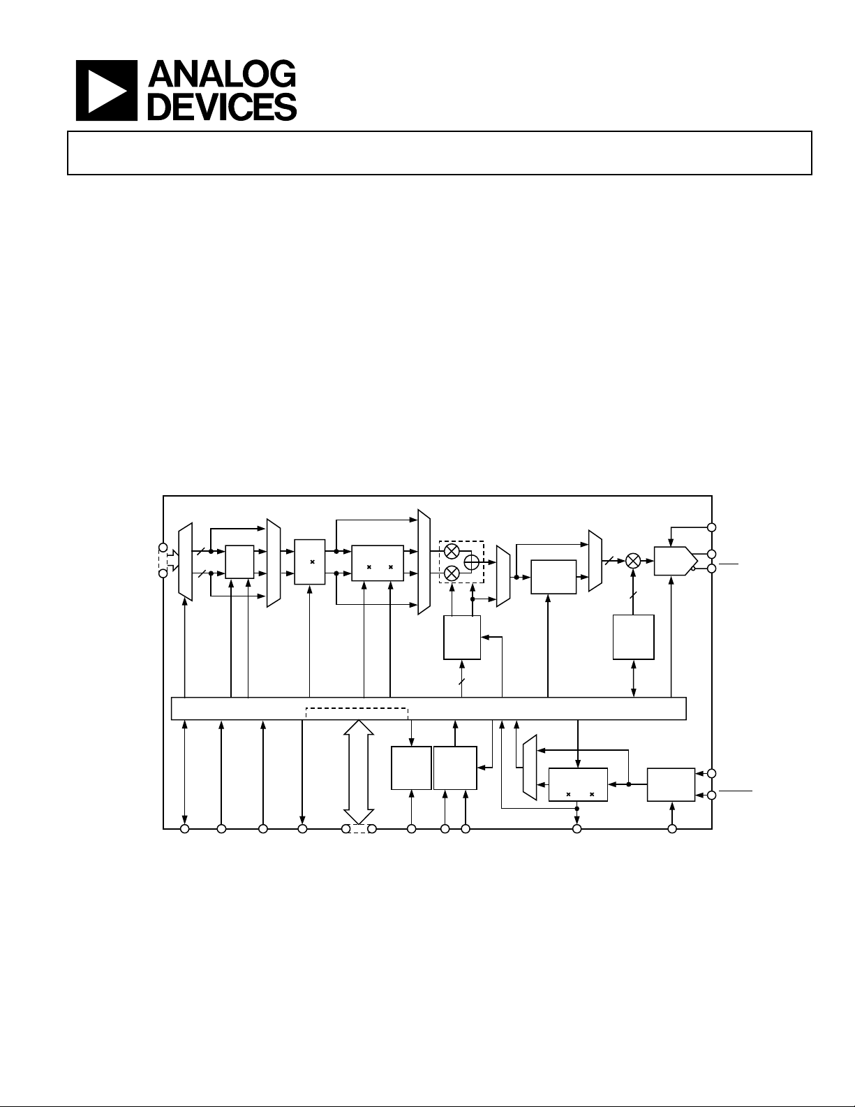
INVERSE
CIC FILTER
I
PARALLEL
DATA IN
(14-BIT)
14
14
DEMUX
Q
DATA CLOCK
INV
CIC
INVERSE CIC CLOCK
OUT
POLATOR
MUX
INVERSE CIC CONTROL
FUNCTIONAL BLOCK DIAGRAM
FIXED
INTER-
PROGRAMMABLE
INTERPOLATOR
(4 )
HALF-BAND CLOCKS
CONTROL REGISTERS
CIC
- 63 )
(2
INTERP CLOCK
INTERP CONTROL
Quadrature Digital Upconverter
AD9857
3.3 V single supply
Single-ended or differential input reference clock
80-lead LQFP surface-mount packaging
Three modes of operation:
Quadrature modulator mode
Single-tone mode
Interpolating DAC mode
APPLICATIONS
HFC data, telephony, and video modems
Wireless base station
Agile, LO frequency synthesis
Broadband communications
QUADRATURE
MODULATOR
MUX
SIN
COS
DDS
CORE
TUNING
32
WORD
TIMING AND CONTROL
MUX
CLOCK
INVERSE
SINC
FILTER
INVERSE
SINC CLOCK
AD9857
14
MUX
8
OUTPUT
SCALE
VALUE
14-BIT
DAC
DAC CLOCK
DAC_RSET
IOUT
IOUT
POWER-
DOWN
LOGIC
PDCLK/
TxENABLE
FUD
Rev. C
Information furnished by Analog Devices is believed to be accurate and reliable.
However, no responsibility is assumed by Analog Devices for its use, nor for any
infringements of patents or other rights of third parties that may result from its use.
Specifications subject to change without notice. No license is granted by implication
or otherwise under any patent or patent rights of Analog Devices. Trademarks and
registered trademarks are the property of their respective owners.
RESET CIC
OVERFLOW
SERIAL
PORT
DIGITAL
POWER-
DOWN
PROFILE
SELECT
LOGIC
Figure 1.
SYNCH
SYSCLK
MUX
CLOCK
MULTIPLIER
(4 – 20 )
PS0PS1
PLL
LOCK
MODE
CONTROL
CLOCK
INPUT
MODE
REFCLK
REFCLK
01018-C-001
One Technology Way, P.O. Box 9106, Norwood, MA 02062-9106, U.S.A.
Tel: 781.329.4700
www.analog.com
Fax: 781.326.8703 © 2004 Analog Devices, Inc. All rights reserved.
Page 2

AD9857
TABLE OF CONTENTS
Revision History ............................................................................... 3
General Description......................................................................... 4
Specifications..................................................................................... 5
Absolute Maximum Ratings............................................................ 8
Explanation of Test Levels........................................................... 8
ESD Caution.................................................................................. 8
Pin Configuration and Function Descriptions............................. 9
Typical Performance Characteristics ........................................... 11
Modulated Output Spectral Plots............................................. 11
Single-Tone Output Spectral Plots ........................................... 12
Narrow-band SFDR Spectral Plots........................................... 13
Output Constellations................................................................ 14
Modes Of Operation ...................................................................... 15
Quadrature Modulation Mode .................................................15
Single-Tone Mode ...................................................................... 16
Interpolating DAC Mode .......................................................... 17
Signal Processing Path ...................................................................18
Input Data Assembler ................................................................ 18
Inverse CIC Filter....................................................................... 19
Programmable (2× to 63×) CIC Interpolating Filter............. 21
Quadrature Modulator .............................................................. 21
DDS Core..................................................................................... 21
Inverse SINC Filter .....................................................................22
Output Scale Multiplier .............................................................22
14-Bit D/A Converter ................................................................ 22
Reference Clock Multiplier .......................................................23
Input Data Programming.............................................................. 24
Control Interface—Serial I/O................................................... 24
General Operation of the Serial Interface............................... 24
Instruction Byte.......................................................................... 26
Serial Interface Port Pin Descriptions..................................... 26
Control Register Descriptions.................................................. 27
Profile #0...................................................................................... 27
Profile #1...................................................................................... 28
Profile #2...................................................................................... 28
Profile #3...................................................................................... 28
Latency......................................................................................... 30
Ease of Use Features....................................................................... 32
Profile Select................................................................................ 32
Setting the Phase of the DDS.................................................... 32
Reference Clock Multiplier....................................................... 32
PLL Lock...................................................................................... 32
Single or Differential Clock ...................................................... 33
CIC Overflow Pin....................................................................... 33
Clearing the CIC Filter ..............................................................33
Digital Power-Down.................................................................. 33
Hardware-Controlled Digital Power-Down ........................... 34
Software-Controlled Digital Power-Down............................. 34
Full Sleep Mode .......................................................................... 34
Power Management Considerations........................................ 34
Support ........................................................................................ 35
Outline Dimensions....................................................................... 38
Ordering Guide .......................................................................... 39
Rev. C | Page 2 of 40
Page 3

AD9857
REVISION HISTORY
5/04−Data Sheet Changed from Rev. B to Rev. C
Changes to 14-Bit D/A Converter Section ..................................22
Changes to Register Address 0Ch, Bit 1 Equation ......................28
Changes to Register Address 12h, Bit 1 Equation.......................28
Changes to Register Address 18h, Bit 1 Equation.......................28
Added Support Section...................................................................35
Updated Figure 38...........................................................................38
Updated Ordering Guide ...............................................................39
4/02—Changed from Rev. A to Rev. B
Edit to Functional Block Diagram..................................................1
Edits to Specifications.......................................................................3
Edits to Figure 5 ................................................................................6
Edits to Figure 18 ............................................................................11
Edits to Figure 19 ............................................................................12
Edits to Figure 20 ............................................................................13
Edits to Figure 25 ........................................................................... 16
Edits to Figure 26 ............................................................................16
Edit to Equation 1 ...........................................................................16
Edit to Figure 28..............................................................................19
Edit to Notes on Serial Port Operation section...........................21
Edit to Figure 37..............................................................................31
Rev. C| Page 3 of 40
Page 4

AD9857
GENERAL DESCRIPTION
The AD9857 integrates a high speed direct digital synthesizer
(DDS), a high performance, high speed, 14-bit digital-to-analog
converter (DAC), clock multiplier circuitry, digital filters, and
other DSP functions onto a single chip, to form a complete
quadrature digital upconverter device. The AD9857 is intended
to function as a universal I/Q modulator and agile upconverter,
single-tone DDS, or interpolating DAC for communications
applications, where cost, size, power dissipation, and dynamic
performance are critical attributes.
The AD9857 offers enhanced performance over the industrystandard AD9856, as well as providing additional features.
The AD9857 is available in a space-saving, surface-mount
package and is specified to operate over the extended industrial
temperature range of −40°C to +85°C.
Rev. C | Page 4 of 40
Page 5

AD9857
SPECIFICATIONS
VS = 3.3 V ± 5%, R
Table 1.
Parameter Temp Test Level Min Typ Max Unit
REF CLOCK INPUT CHARACTERISTICS
Frequency Range
REFCLK Multiplier Disabled Full VI 1 200 MHz
REFCLK Multiplier Enabled at 4× Full VI 1 50 MHz
REFCLK Multiplier Enabled at 20× Full VI 1 10 MHz
Input Capacitance 25°C V 3 pF
Input Impedance 25°C V 100 MΩ
Duty Cycle 25°C V 50 %
Duty Cycle with REFCLK Multiplier Enabled 25°C V 35 65 %
Differential Input (VDD/2) ±200 mV 25°C V 1.45 1.85 V
DAC OUTPUT CHARACTERISTICS
Resolution 14 Bits
Full-Scale Output Current 5 10 20 mA
Gain Error 25°C I 8.5 0 % FS
Output Offset 25°C I 2 µA
Differential Nonlinearity 25°C V 1.6 LSB
Integral Nonlinearity 25°C V 2 LSB
Output Capacitance 25°C V 5 pF
Residual Phase Noise @ 1 kHz Offset, 40 MHz A
REFCLK Multiplier Enabled at 20× 25°C V −107 dBc/Hz
REFCLK Multiplier at 4× 25°C V −123 dBc/Hz
REFCLK Multiplier Disabled 25°C V −145 dBc/Hz
Voltage Compliance Range 25°C I −0.5 +1.0 V
Wideband SFDR
1 MHz to 20 MHz Analog Out 25°C V −75 dBc
20 MHz to 40 MHz Analog Out 25°C V −65 dBc
40 MHz to 60 MHz Analog Out 25°C V −62 dBc
60 MHz to 80 MHz Analog Out 25°C V −60 dBc
Narrowband SFDR
10 MHz Analog Out (±1 MHz) 25°C V −87 dBc
10 MHz Analog Out (±250 kHz) 25°C V −88 dBc
10 MHz Analog Out (±50 kHz) 25°C V −92 dBc
10 MHz Analog Out (±10 kHz) 25°C V −94 dBc
65 MHz Analog Out (±1 MHz) 25°C V −86 dBc
65 MHz Analog Out (±250 kHz) 25°C V −86 dBc
65 MHz Analog Out (±50 kHz) 25°C V −86 dBc
65 MHz Analog Out (±10 kHz) 25°C V −88 dBc
80 MHz Analog Out (±1 MHz) 25°C V −85 dBc
80 MHz Analog Out (±250 kHz) 25°C V −85 dBc
80 MHz Analog Out (±50 kHz) 25°C V −85 dBc
80 MHz Analog Out (±0 kHz) 25°C V −86 dBc
= 1.96 kΩ, external reference clock frequency = 10 MHz with REFCLK multiplier enabled at 20×.
SET
OUT
Rev. C| Page 5 of 40
Page 6

AD9857
Parameter Temp Test Level Min Typ Max Unit
MODULATOR CHARACTERISTICS (65 MHz A
(Input data: 2.5 MS/s, QPSK, 4× oversampled, inverse SINC
filter ON, inverse CIC ON)
I/Q Offset 25°C IV 55 65 dB
Error Vector Magnitude 25°C IV 0.4 1 %
INVERSE SINC FILTER (variation in gain from DC to 80 MHz,
inverse SINC filter ON)
SPURIOUS POWER (off channel, measured in equivalent
bandwidth), Full-Scale Output
6.4 MHz Bandwidth 25°C IV −65 dBc
3.2 MHz Bandwidth 25°C IV −67 dBc
1.6 MHz Bandwidth 25°C IV −69 dBc
0.8 MHz Bandwidth 25°C IV −69 dBc
0.4 MHz Bandwidth 25°C IV −70 dBc
0.2 MHz Bandwidth 25°C IV −72 dBc
SPURIOUS POWER (Off channel, measured in equivalent
bandwidth), Output Attenuated 18 dB
Relative to Full Scale
6.4 MHz Bandwidth 25°C IV −51 dBc
3.2 MHz Bandwidth 25°C IV −54 dBc
1.6 MHz Bandwidth 25°C IV −56 dBc
0.8 MHz Bandwidth 25°C IV −59 dBc
0.4 MHz Bandwidth 25°C IV −62 dBc
0.2 MHz Bandwidth 25°C IV −63 dBc
TIMING CHARACTERISTICS
Serial Control Bus
Maximum Frequency 25°C I 10 MHz
Minimum Clock Pulse Width Low (t
Minimum Clock Pulse Width High (t
Maximum Clock Rise/Fall Time 25°C I 1 ms
Minimum Data Setup Time (tDS) 25°C I 30 ns
Minimum Data Hold Time (tDH) 25°C I 0 ns
Maximum Data Valid Time (tDV) 25°C I 35 ns
Wake-Up Time1 25°C I 1 ms
Minimum RESET Pulse Width High (tRH) 25°C I 5 SYSCLK22Cycles
Minimum CS Setup Time
CMOS LOGIC INPUTS
Logic 1 Voltage 25°C IV 2.0 V
Logic 0 Voltage 25°C IV 0.8 V
Logic 1 Current 25°C I 5 µA
Logic 0 Current 25°C I 5 µA
Input Capacitance 25°C V 3 pF
CMOS LOGIC OUTPUTS (1 mA LOAD)
Logic 1 Voltage 25°C I 2.7 V
Logic 0 Voltage 25°C I 0.4 V
OUT
)
25°C V ±0.1 dB
) 25°C I 30 ns
PWL
) 25°C I 30 ns
PWH
25°C I 40 ns
Rev. C | Page 6 of 40
Page 7

AD9857
Parameter Temp Test Level Min Typ Max Unit
POWER SUPPLY VSCURRENT3 (all power specifications at
= 3.3 V, 25°C, REFCLK = 200 MHz)
V
DD
Full Operating Conditions 25°C I 540 615 mA
160 MHz Clock (×16) 25°C I 445 515 mA
120 MHz Clock (×12) 25°C I 345 400 mA
Burst Operation (25%) 25°C I 395 450 mA
Single-Tone Mode 25°C I 265 310 mA
Power-Down Mode 25°C I 71 80 mA
Full-Sleep Mode 25°C I 8 13.5 mA
1
Wake-up time refers to recovery from full-sleep mode. The longest time required is for the reference clock multiplier PLL to lock up (if it is being used). The wake-up
time assumes that there is no capacitor on DAC_BP, and that the recommended PLL loop filter values are used. The state of the reference clock multiplier lock can be
determined by observing the signal on the PLL_LOCK pin.
2
SYSCLK refers to the actual clock frequency used on-chip by the AD9857. If the reference clock multiplier is used to multiply the external reference frequency, the
SYSCLK frequency is the external frequency multiplied by the reference clock multiplier multiplication factor. If the reference clock multiplier is not used, the SYSCLK
frequency is the same as the external REFCLK frequency.
3
CIC = 2, INV SINC ON, FTW = 40%, PLL OFF, auto power-down between burst On, TxENABLE duty cycle = 25%.
Rev. C| Page 7 of 40
Page 8
AD9857
ABSOLUTE MAXIMUM RATINGS
Stresses above those listed under Absolute Maximum Ratings
may cause permanent damage to the device. This is a stress
rating only; functional operation of the device at these or any
other conditions above those indicated in the operational
section of this specification is not implied. Exposure to absolute
maximum rating conditions for extended periods may affect
device reliability.
Table 2.
Parameter Rating
Maximum Junction Temperature 150°C
V
S
Digital Input Voltage −0.7 V to +V
Digital Output Current 5 mA
Storage Temperature −65°C to +150°C
Operating Temperature −40°C to +85°C
Lead Temperature (Soldering 10 s) 300°C
θ
JA
θ
JC
4 V
S
35°C/W
16°C/W
EXPLANATION OF TEST LEVELS
Table 3.
Test Level
1 100% production tested.
2
3 Sample tested only.
4
5 Parameter is a typical value only.
6
100% production tested at 25°C and sample tested at
specific temperatures.
Parameter is guaranteed by design and
characterization testing.
Devices are 100% production tested at 25°C and
guaranteed by design and characterization testing for
industrial operating temperature range.
ESD CAUTION
ESD (electrostatic discharge) sensitive device. Electrostatic charges as high as 4000 V readily accumulate on
the human body and test equipment and can discharge without detection. Although this product features
proprietary ESD protection circuitry, permanent damage may occur on devices subjected to high energy
electrostatic discharges. Therefore, proper ESD precautions are recommended to avoid performance
degradation or loss of functionality.
Rev. C | Page 8 of 40
Page 9
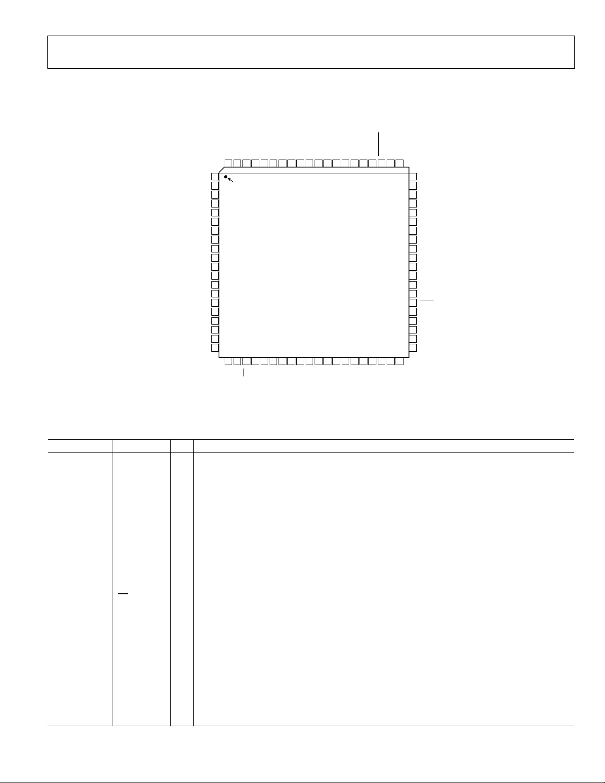
AD9857
PIN CONFIGURATION AND FUNCTION DESCRIPTIONS
RESET
DPD
AGND
AVDD
REFCLK
REFCLK
AVDD
AVDD
AGND
AGND
AGND
60
DIFFCLKEN
59
AGND
58
AVDD
57
NC
56
AGND
55
PLL_FILTER
54
AVDD
53
AGND
52
NC
51
NC
50
DAC_RSET
49
DAC_BP
48
AVDD
47
AGND
46
IOUT
45
IOUT
44
AGND
43
AVDD
42
AGND
41
NC
01018-C-000
TxENABLE
PDCLK/FUD
DGND
DGND
DGND
DVDD
DVDD
DVDD
DGND
DGND
DGND
CIC_OVRFL
DVDD
DGND
PLL_LOCK
34 35 36 37 38 39 40
NC
AVDD
DVDD
DVDD
AGND
64 63 62 6167 66 65
D13
D12
D11
D10
D9
D8
D7
DVDD
DVDD
DVDD
DGND
DGND
DGND
D6
D5
D4
D3
D2
D1
D0
NC = NO CONNECT
80 79 78 77 76 71 70 69 6875 74 73 72
1
PIN 1
2
INDICATOR
3
4
5
6
7
8
9
10
11
12
13
14
15
16
17
18
19
20
21 22 23 24 25 26 27 28 29 30 31 32 33
CS
PS1
PS0
SDIO
SCLK
SDO
SYNCIO
AD9857
TOP VIEW
(Not to Scale)
DGND
DGND
Figure 2. Pin Configuration
Table 4. Pin Function Descriptions
Pin Number Mnemonic I/O Function
20–14, 7–1
D0–D6, D7–
D13
I
14-Bit Parallel Data Bus for I and Q Data. The required numeric format is twos complement with D13
as the sign bit and D12–D0 as the magnitude bits. Alternating 14-bit words are demultiplexed onto
the I and Q data pathways (except when operating in the interpolating DAC mode, in which case
every word is routed onto the I data path). When the TxENABLE pin is asserted high, the next
accepted word is presumed to be I data, the next Q data, and so forth.
8–10, 31–33,
DVDD 3.3 V Digital Power pin(s).
73–75
11–13, 28–30,
DGND Digital Ground pin(s).
70–72, 76–78
21 PS1 I
Profile Select Pin 1. The LSB of the two profile select pins. In conjunction with PS0, selects one of four
profile configurations.
22 PS0 I
Profile Select Pin 0. The MSB of the two profile select pins. In conjunction with P1, selects one of four
profile configurations.
23
CS
I
Serial Port Chip Select pin. An active low signal that allows multiple devices to operate on a single
serial bus.
24 SCLK I Serial Port Data Clock pin. The serial data CLOCK for the serial port.
25 SDIO I/O
Serial Port Input/Output Data pin. Bidirectional serial DATA pin for the serial port. This pin can be
programmed to operate as a serial input only pin, via the control register bit 00h<7>. The default
state is bidirectional.
26 SDO O
Serial Port Output Data pin. This pin serves as the serial data output pin when the SDIO pin is
configured for serial input only mode. The default state is three-state.
27 SYNCIO I
Serial Port Synchronization pin. Synchronizes the serial port without affecting the programmable
register contents. This is an active high input that aborts the current serial communication cycle.
34, 41, 51, 52,
NC No connect.
57
Rev. C| Page 9 of 40
Page 10

AD9857
Pin Number Mnemonic I/O Function
35, 37, 38, 43,
48, 54, 58, 64
36, 39, 40, 42,
44, 47, 53, 56,
59, 61, 65
45 IOUT O DAC Output pin. Normal DAC output current (analog).
46
49 DAC_BP DAC Reference Bypass. Typically not used.
50 DAC_RSET I DAC Current Set pin. Sets DAC reference current.
55 PLL_FILTER O PLL Filter. R-C network for PLL filter.
60 DIFFCLKEN I
62 REFCLK I
63
66 DPD I
67 RESET I Hardware RESET pin. An active high input that forces the device into a predefined state.
68 PLL_LOCK O PLL Lock pin. Active high output signifying, in real time, when PLL is in lock state.
69 CIC_OVRFL O
79 PDCLK/FUD I/O
80 TxENABLE I
AVDD 3.3 V Analog Power pin(s).
AGND Analog Ground pin(s).
IOUT
REFCLK
O DAC Complementary Output pin. Complementary DAC output current (analog).
Clock Mode Select pin. A logic high on this pin selects DIFFERENTIAL REFCLK input mode. A logic
low selects the SINGLE-ENDED REFCLK input mode.
Reference Clock pin. In single-ended clock mode, this pin is the Reference Clock input. In differential
clock mode, this pin is the positive clock input.
I Inverted Reference Clock pin. In differential clock mode, this pin is the negative clock input.
Digital Power-Down pin. Assertion of this pin shuts down the digital sections of the device to
conserve power. However, if selected, the PLL remains operational.
CIC Overflow pin. Activity on this pin indicates that the CIC Filters are in “overflow” state. This pin is
typically low unless a CIC overflow occurs.
Parallel Data Clock/Frequency Update pin. When not in single-tone mode, this pin is an output
signal that should be used as a clock to synchronize the acceptance of the 14-bit parallel
data-words on Pins D13–D0. In single-tone mode, this pin is an input signal that synchronizes the
transfer of a changed frequency tuning word (FTW) in the active profile (PSx) to the accumulator
(FUD = frequency update signal). When profiles are changed by means of the PS–PS1 pins, the FUD
does not have to be asserted to make the FTW active.
When TxENABLE is asserted, the device processes the data through the I and Q data pathways;
otherwise 0s are internally substituted for the I and Q data entering the signal path. The first data
word accepted when the TxENABLE is asserted high is treated as I data, the next data word is Q data,
and so forth.
Rev. C | Page 10 of 40
Page 11
AD9857
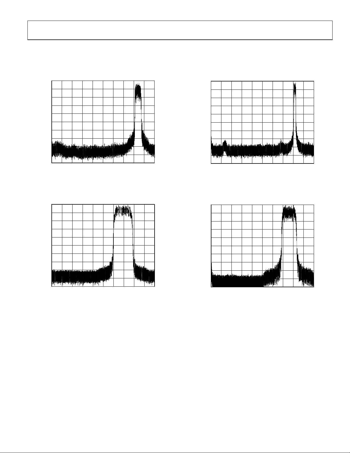
TYPICAL PERFORMANCE CHARACTERISTICS
MODULATED OUTPUT SPECTRAL PLOTS
0
–10
–20
–30
–40
–50
dB
–60
–70
–80
–90
–100
START 0Hz 5MHz/ STOP 50MHz
Figure 3. QPSK at 42 MHz and 2.56 MS/s; 10.24 MHz External Clock
with REFCLK Multiplier = 12, CIC Interpolation Rate = 3,
4× Oversampled Data
0
–8
–16
–24
–32
–40
dB
–48
–56
–64
–72
–80
START 0Hz 4MHz/ STOP 40MHz
Figure 4. 64-QAM at 28 MHz and 6 MS/s; 36 MHz External Clock
with REFCLK Multiplier = 4, CIC Interpolation Rate = 2,
3× Oversampled Data
01018-C-003
01018-C-004
0
–10
–20
–30
–40
–50
dB
–60
–70
–80
–90
–100
START 0Hz 8MHz/ STOP 80MHz
01018-C-005
Figure 5. 16-QAM at 65 MHz and 1.28 MS/s; 10.24 MHz External Clock
with REFCLK Multiplier = 18, CIC Interpolation Rate = 9,
4× Oversampled Data
0
–8
–16
–24
–32
–40
dB
–48
–56
–64
–72
–80
START 0HzSTART 0Hz 5MHz/ STOP 50MHz
Figure 6. 256-QAM at 38 MHz and 6 MS/s; 48 MHz External Clock
with REFCLK Multiplier = 4, CIC Interpolation Rate = 2,
4× Oversampled Data
01018-C-006
Rev. C| Page 11 of 40
Page 12
AD9857
SINGLE-TONE OUTPUT SPECTRAL PLOTS
0
–10
–20
–30
–40
–50
dB
–60
–70
–80
–90
–100
START 0Hz 10MHz/ STOP 100MHz
Figure 7. 21 MHz Single-Tone Output
0
–10
–20
–30
–40
–50
dB
–60
–70
–80
–90
–100
START 0Hz
Figure 8. 65 MHz Single-Tone Output
10MHz/ STOP 100MHz
01018-C-007
01018-C-008
0
–10
–20
–30
–40
–50
dB
–60
–70
–80
–90
–100
START 0Hz 10MHz/ STOP 100MHz
Figure 9. 42 MHz Single-Tone Output
0
–10
–20
–30
–40
–50
dB
–60
–70
–80
–90
–100
START 0Hz 10MHz/ STOP 100MHz
Figure 10. 79 MHz Single-Tone Output
01018-C-009
01018-C-010
Rev. C | Page 12 of 40
Page 13

AD9857
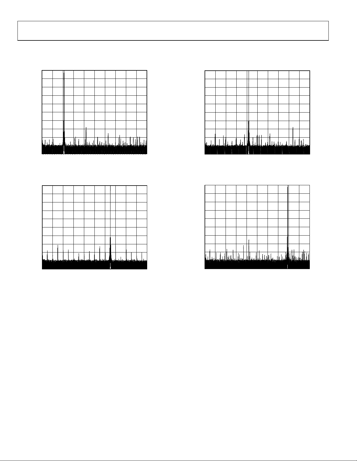
NARROW-BAND SFDR SPECTRAL PLOTS
0
–10
–20
–30
–40
–50
dB
–60
–70
–80
–90
–100
CENTER 70.1MHz
10kHz/ SPAN 100kHz
Figure 11. 70.1 MHz Narrow-Band SFDR, 10 MHz External Clock
with REFCLK Multiplier = 20
01018-C-011
0
–10
–20
–30
–40
–50
dB
–60
–70
–80
–90
–100
CENTER 70.1MHz
10kHz/ SPAN 100kHz
Figure 12. 70.1 MHz Narrow-Band SFDR, 200 MHz External Clock
with REFCLK Multiplier Disabled
01018-C-012
Rev. C| Page 13 of 40
Page 14

AD9857
2
2
2
OUTPUT CONSTELLATIONS
1
1
CONST
200m/DIV
–1
–1.3071895838 1.30718958378
Figure 13. QPSK, 65 MHz, 2.56 MS/s
1
CONST
00m/DIV
–1
–1.3071895838 1.30718958378
Figure 14. 64-QAM, 42 MHz, 6 MS/s
1
01018-C-013
01018-C-014
CONST
200m/DIV
–1
–1.3071895838 1.30718958378
Figure 16. 16-QAM, 65 MHz, 2.56 MS/s
1
CONST
00m/DIV
–1
–1.3071895838 1.30718958378
Figure 17. 256-QAM, 42 MHz, 6 MS/s
01018-C-016
01018-C-017
CONST
00m/DIV
–1
–1.3071895838 1.30718958378
01018-C-015
Figure 15. GMSK Modulation, 13 MS/s
Rev. C | Page 14 of 40
Page 15

AD9857
MODES OF OPERATION
The AD9857 has three operating modes:
• Quadrature modulation mode (default)
• Single-tone mode
• Interpolating DAC mode
Mode selection is accomplished by programming a control
register via the serial port. The inverse SINC filter and output
scale multiplier are available in all three modes.
QUADRATURE MODULATION MODE
In quadrature modulation mode, both the I and Q data paths
are active. A block diagram of the AD9857 operating in the
quadrature modulation mode is shown in Figure 18.
In quadrature modulation mode, the PDCLK/FUD pin is an
output and functions as the parallel data clock (PDCLK), which
serves to synchronize the input of data to the AD9857. In this
mode, the input data must be synchronized with the rising edge
of PDCLK. The PDCLK operates at twice the rate of either the I
or Q data path. This is due to the fact that the I and Q data must
be presented to the parallel port as two 14-bit words
multiplexed in time. One I word and one Q word together
comprise one internal sample. Each sample is propagated along
the internal data pathway in parallel fashion.
The DDS core provides a quadrature (sin and cos) local
oscillator signal to the quadrature modulator, where the I and Q
data are multiplied by the respective phase of the carrier and
summed together, to produce a quadrature-modulated data
stream.
All of this occurs in the digital domain, and only then is the
digital data stream applied to the 14-bit DAC to become the
quadrature-modulated analog output signal.
PARALLEL
DATA IN
(14-BIT)
DATA CLOCK
PDCLK/
FUD
I
14
14
DEMUX
Q
TxENABLE
INVERSE
CIC FILTER
INV
CIC
INVERSE CIC CLOCK
INVERSE CIC CONTROL
FIXED
INTER-
POLATOR
MUX
RESET CIC
OVERFLOW
PROGRAMMABLE
INTERPOLATOR
(4 )
HALF-BAND CLOCKS
CONTROL REGISTERS
(2
INTERP CONTROL
SERIAL
PORT
CIC
- 63 )
Figure 18. Quadrature Modulation Mode
INTERP CLOCK
POWER-
DOWN
LOGIC
DIGITAL
POWER-
DOWN
QUADRATURE
MODULATOR
MUX
SIN
COS
DDS
CORE
TUNING
32
WORD
TIMING AND CONTROL
PROFILE
SELECT
LOGIC
SYNCH
PS0PS1
MUX
CLOCK
SYSCLK
INVERSE
SINC
FILTER
INVERSE
SINC CLOCK
MUX
MULTIPLIER
CLOCK
(4
PLL
LOCK
– 20 )
AD9857
14
MUX
8
OUTPUT
SCALE
VALUE
14-BIT
DAC
DAC CLOCK
MODE
CONTROL
CLOCK
INPUT
MODE
DAC_RSET
IOUT
IOUT
REFCLK
REFCLK
01018-C-018
Rev. C| Page 15 of 40
Page 16

AD9857
SINGLE-TONE MODE
A block diagram of the AD9857 operating in the single-tone
mode is shown in Figure 19. In the single-tone mode, both the
I and Q data paths are disabled from the 14-bit parallel data
port up to and including the modulator. The PDCLK/ FUD pin
is an input and functions as a frequency update (FUD) control
signal. This is necessary because the frequency tuning word is
programmed via the asynchronous serial port. The FUD signal
causes the new frequency tuning word to become active.
In single-tone mode, the cosine portion of the DDS serves as
the signal source. The output signal consists of a single
frequency as determined by the tuning word stored in the
appropriate control register, per each profile.
In the single-tone mode, no 14-bit parallel data is applied to the
AD9857. The internal DDS core is used to produce a single
frequency signal according to the tuning word. The single-tone
signal then moves toward the output, where the inverse SINC
filter and the output scaling can be applied. Finally, the digital
single-tone signal is converted to the analog domain by the
14-bit DAC.
AD9857
PDCLK/
FUD
CONTROL REGISTERS
RESET SERIAL
PORT
DDS
CORE
TUNING
WORD
TIMING AND CONTROL
POWER-
DOWN
LOGIC
DIGITAL
POWER-
DOWN
PROFILE
SELECT
LOGIC
PS0PS1
Figure 19. Single-Tone Mode
COS
DAC_RSET
14
CLOCK
(4
PLL
LOCK
MUX
OUTPUT
– 20 )
INVERSE
SINC
FILTER
INVERSE
SYSCLK
SINC CLOCK
MUX
MULTIPLIER
CLOCK
32
SYNCH
8
SCALE
VALUE
14-BIT
DAC
DAC CLOCK
MODE
CONTROL
CLOCK
INPUT
MODE
IOUT
IOUT
REFCLK
REFCLK
01018-C-001
Rev. C | Page 16 of 40
Page 17

AD9857
INTERPOLATING DAC MODE
A block diagram of the AD9857 operating in the interpolating
DAC mode is shown in Figure 20. In this mode, the DDS and
modulator are both disabled and only the I data path is active.
The Q data path is disabled from the 14-bit parallel data port up
to and including the modulator.
As in the quadrature modulation mode, the PDCLK pin is an
output and functions as a clock which serves to synchronize the
input of data to the AD9857. Unlike the quadrature modulation
mode, however, the PDCLK operates at the rate of the I data
path. This is because only I data is being presented to the
parallel port as opposed to the interleaved I/Q format of the
quadrature modulation mode.
In the Interpolating DAC mode, the baseband data supplied at
the parallel port remains at baseband at the output; that is, no
modulation takes place. However, a sample rate conversion
takes place based on the programmed interpolation rate. The
interpolation hardware performs the necessary signal
processing required to eliminate the aliased images at baseband
that would otherwise result from a sample rate conversion. The
interpolating DAC function is effectively an oversampling
operation with the original input spectrum intact but sampled
at a higher rate.
PARALLEL
DATA IN
(14-BIT)
I
14
DEMUX
DATA CLOCK
PDCLK/
FUD
INVERSE
CIC FILTER
INV
CIC
INVERSE CIC CLOCK
TxENABLE
INVERSE CIC CONTROL
FIXED
INTER-
POLATOR
(4 )
MUX
HALF-BAND CLOCKS
RESET CIC
OVERFLOW
PROGRAMMABLE
INTERPOLATOR
CIC
(2
- 63 )
INTERP CLOCK
INTERP CONTROL
CONTROL REGISTERS
POWER-
SERIAL
PORT
DIGITAL
POWER-
MUX
TIMING AND CONTROL
PROFILE
DOWN
SELECT
LOGIC
DOWN
LOGIC
AD9857
DAC_RSET
14
INVERSE
SINC
FILTER
INVERSE
SINC CLOCK
SYNCH
SYSCLK
MUX
PS0PS1
MUX
CLOCK
MULTIPLIER
(4
– 20 )
PLL
LOCK
OUTPUT
SCALE
VALUE
14-BIT
DAC
8
DAC CLOCK
MODE
CONTROL
CLOCK
INPUT
MODE
IOUT
IOUT
REFCLK
REFCLK
01018-C-001
Figure 20. Interpolating DAC Mode
Rev. C| Page 17 of 40
Page 18

AD9857
SIGNAL PROCESSING PATH
To better understand the operation of the AD9857 it is helpful
to follow the signal path from input, through the device, to the
output, examining the function of each block (refer to Figure 1).
The input to the AD9857 is a 14-bit parallel data path. This
assumes that the user is supplying the data as interleaved I and
Q values. Any encoding, interpolation, and pulse shaping of the
data stream should occur before the data is presented to the
AD9857 for upsampling.
The AD9857 demultiplexes the interleaved I and Q data into
two separate data paths inside the part. This means that the
input sample rate (f
presented to the AD9857, must be 2× the internal I/Q Sample
Rate (f
words, f
), the rate at which the I/Q pairs are processed. In other
IQ
= 2 × fIQ.
DATA
From the input demultiplexer to the quadrature modulator, the
data path of the AD9857 is a dual I/Q path.
All timing within the AD9857 is provided by the internal
system clock (SYSCLK) signal. The externally provided
reference clock signal may be used as is (1×), or multiplied by
the internal clock multiplier (4×−20×) to generate the SYSCLK.
All other internal clocks and timing are derived from the
SYSCLK.
INPUT DATA ASSEMBLER
In the quadrature modulation or interpolating DAC modes, the
device accepts 14-bit, twos complement data at its parallel data
port. The timing of the data supplied to the parallel port may be
easily facilitated with the PDCLK/FUD pin of the AD9857,
which is an output in the quadrature modulation mode and the
interpolating DAC mode. In the single-tone mode, the same pin
becomes an input to the device and serves as a frequency
update (FUD) strobe.
Frequency control words are programmed into the AD9857 via
the serial port (see the Control Register description). Because
the serial port is an asynchronous interface, when programming
new frequency tuning words into the on-chip profile registers,
the AD9857’s internal frequency synthesizer must be
synchronized with external events. The purpose of the FUD
input pin is to synchronize the start of the frequency
synthesizer to the external timing requirements of the user. The
rising edge of the FUD signal causes the frequency tuning word
of the selected profile (see the Profile section) to be transferred
), the rate at which 14-bit words are
DATA
to the accumulator of the DDS, thus starting the frequency
synthesis process.
After loading the frequency tuning word to a profile, a FUD
signal is not needed when switching between profiles using the
two profile select pins (PS0, PS1). When switching between
profiles, the frequency tuning word in the profile register
becomes effective.
In the quadrature modulation mode, the PDCLK rate is twice
the rate of the I (or Q) data rate. The AD9857 expects
interleaved I and Q data words at the parallel port with one
word per PDCLK rising edge. One I word and one Q word
together comprise one internal sample. Each sample is
propagated along the internal data pathway in parallel.
In the interpolating DAC mode, however, the PDCLK rate is the
same as the I data rate because the Q data path is inactive. In
this mode, each PDCLK rising edge latches a data word into the
I data path.
The PDCLK is provided as a continuous clock (i.e., always
active). However, the assertion of PDCLK may be optionally
qualified internally by the PLL lock indicator if the user elects
to set the PLL lock control bit in the appropriate control register.
Data supplied by the user to the 14-bit parallel port is latched
into the device coincident with the rising edge of the PDCLK.
In the quadrature modulation mode, the rising edge of the
TxENABLE signal is used to synchronize the device. While
TxENABLE is in the Logic 0 state, the device ignores the 14-bit
data applied to the parallel port and allows the internal data
path to be flushed by forcing 0s down the I and Q data pathway.
On the rising edge of TxENABLE, the device is ready for the
first I word. The first I word is latched into the device
coincident with the rising edge of PDCLK. The next rising edge
of PDCLK latches in a Q word, etc., until TxENABLE is set to a
Logic 0 state by the user.
When in the quadrature modulation mode, it is important that
the user ensure that an even number of PDCLK intervals are
observed during any given TxENABLE period. This is because
the device must capture both an I and a Q value before the data
can be processed along the internal data pathway.
The timing relationship between TxENABLE, PDCLK, and
DATA is shown in Figure 21 and Figure 22.
Rev. C | Page 18 of 40
Page 19

AD9857
TxENABLE
PDCLK
D<13:0>
t
DS
t
DS
I
0
t
DH
Q
0
Figure 21. 14-Bit Parallel Port Timing Diagram—Quadrature Modulation Mode
TxENABLE
PDCLK
D<13:0>
t
DS
t
DS
I
0
t
DH
I
1
Figure 22. 14-Bit Parallel Port Timing Diagram—Interpolating DAC Mode
Table 5. Parallel Data Bus Timing
Symbol Definition Minimum
tDS Data Setup Time 4 ns
tDH Data Hold Time 0 ns
INVERSE CIC FILTER
The inverse cascaded integrator comb (CIC) filter precompensates the data to offset the slight attenuation gradient imposed
by the CIC filter. See the Programmable (2× to 63×) CIC
Interpolating Filter section. The I (or Q) data entering the first
half-band filter occupies a maximum bandwidth of one-half
as defined by Nyquist (where f
f
DATA
input of the first half-band filter). This is shown graphically in
Figure 23.
INBAND
ATTENUATION
GRADIENT
is the sample rate at the
DATA
t
DH
I
1
I
2
Q
1
I
3
I
I
K– 1
N
t
DH
Q
N
01018-C-021
I
K
01018-C-022
If the CIC filter is employed, the inband attenuation gradient
could pose a problem for those applications requiring an
extremely flat pass band. For example, if the spectrum of the
data as supplied to the AD9857 I or Q path occupies a
significant portion of the one-half f
region, the higher
DATA
frequencies of the data spectrum receives slightly more
attenuation than the lower frequencies (the worst-case overall
droop from f = 0 to one-half f
is < 0.8 dB). This may not be
DATA
acceptable in certain applications. The inverse CIC filter has a
response characteristic that is the inverse of the CIC filter
response over the one-half f
DATA
region.
The net result is that the product of the two responses yields in
an extremely flat pass band, thereby eliminating the inband
attenuation gradient introduced by the CIC filter. The price
to be paid is a slight attenuation of the input signal of approximately 0.5 dB for a CIC interpolation rate of 2 and 0.8 dB for
interpolation rates of 3 to 63.
f
DATA
CIC FILTER RESPONSE
f
DATA
/2
Figure 23. CIC Filter Response
The inverse CIC filter is implemented as a digital FIR filter
with a response characteristic that is the inverse of the
programmable CIC interpolator. The product of the two
responses yields a nearly flat response over the baseband
Nyquist bandwidth. The inverse CIC filter provides frequency
compensation that yields a response flatness of ±0.05 dB over
the baseband Nyquist bandwidth, allowing the AD9857 to
provide excellent SNR over its performance range.
f
4f
DATA
01018-C-023
The inverse CIC filter can be bypassed by setting Control
Register 06h<0>. It is automatically bypassed if the CIC
interpolation rate is 1×. Whenever this stage is bypassed, power
to the stage is shutoff, thereby reducing power dissipation.
Rev. C| Page 19 of 40
Page 20

AD9857
Fixed Interpolator (4×)
This block is a fixed 4× interpolator. It is implemented as two
half-band filters. The output of this stage is the original data
upsampled by 4×.
Before presenting a detailed description of the half-band filters,
recall that in the case of the quadrature modulation mode the
input data stream is representative of complex data; i.e., two
input samples are required to produce one I/Q data pair. The
I/Q sample rate is one-half the input data rate. The I/Q sample
rate (the rate at which I or Q samples are presented to the input
of the first half-band filter) is referred to as f
AD9857 is a quadrature modulator, f
IQ
. Because the
IQ
represents the baseband
of the internal I/Q sample pairs. It should be emphasized here
is not the same as the baseband of the user’s symbol rate
that f
IQ
data, which must be upsampled before presentation to the
AD9857 (as explained later). The I/Q sample rate (f
limit on the minimum bandwidth necessary to transmit the f
) puts a
IQ
IQ
spectrum. This is the familiar Nyquist limit and is equal to one-
, hereafter referred to as f
half f
IQ
NYQ
.
Together, the two half-band filters provide a factor-of-four
increase in the sampling rate (4 × f
or 8 × f
IQ
NYQ
). Their
combined insertion loss is 0.01 dB, so virtually no loss of signal
level occurs through the two half-band filters. Both half-band
filters are linear phase filters, so that virtually no phase
distortion is introduced within the pass band of the filters. This
is an important feature as phase distortion is generally
intolerable in a data transmission system.
The half-band filters are designed so that their composite
performance yields a usable pass band of 80% of the baseband
Nyquist frequency (0.2 on the frequency scale below). Within
that pass band, the ripple does not exceed 0.002 dB. The stop
band extends from 120% to 400% of the baseband Nyquist
frequency (0.3 to 1.0 on the frequency scale) and offers a
minimum of 85 dB attenuation. Figure 24 and Figure 25 show
the composite response of the two half-band filters together.
10
0
0.2
–10
–20
–30
–40
–50
–60
–70
–80
SAMPLE RATE
–90
–100
–110
–120
–130
–140
0 0.2 0.4
Figure 24. Half-Band 1 and 2 Frequency Response; Frequency
0.3
0.6 0.8 1.0 1.2 1.4 1.6 1.8 2.0
FREQUENCY
Relative to HB1 Output Sample Rate
–85
01018-C-024
0.010
0.008
0.006
0.004
0.002
0
GAIN (dB)
–0.002
–0.004
–0.006
–0.008
–0.010
0
Figure 25. Combined Half-Band 1 and 2 Pass Band Detail;
The usable bandwidth of the filter chain puts a limit on the
maximum data rate that can be propagated through the
0.05 0.10 0.15 0.20 0.25
RELATIVE FREQUENCY (HB1 OUTPUT SAMPLE RATE = 1)
Frequency Relative to HB1 Output Sample Rate
01018-C-025
AD9857. A look at the pass band detail of the half-band filter
response (Figure 25) indicates that in order to maintain an
amplitude error of no more than 1 dB, signals are restricted to
having a bandwidth of no more than about 90% of f
. Thus, to
NYQ
keep the bandwidth of the data in the flat portion of the filter
pass band, the user must oversample the baseband data by at
least a factor of two prior to presenting it to the AD9857. Note
that without oversampling, the Nyquist bandwidth of the
baseband data corresponds to the f
. Because of this, the
NYQ
upper end of the data bandwidth suffers 6 dB or more of
attenuation due to the frequency response of the half-band
filters. Furthermore, if the baseband data applied to the AD9857
has been pulse shaped, there is an additional concern.
Typically, pulse shaping is applied to the baseband data via a
filter having a raised cosine response. In such cases, an α value is
used to modify the bandwidth of the data where the value of α
is such that ≤ α ≤ 1. A value of 0 causes the data bandwidth to
correspond to the Nyquist bandwidth. A value of 1 causes the
data bandwidth to be extended to twice the Nyquist bandwidth.
Thus, with 2× oversampling of the baseband data and α = 1, the
Nyquist bandwidth of the data corresponds with the I/Q
Nyquist bandwidth. As stated earlier, this results in problems
near the upper edge of the data bandwidth due to the roll-off
attenuation of the half-band filters. Figure 26 illustrates the
relationship between α and the bandwidth of raised cosine
shaped pulses. The problem area is indicated by the shading in
the tail of the pulse with α = 1 which extends into the roll-off
region of the half-band filter.
The effect of raised cosine filtering on baseband pulse
bandwidth, and the relationship to the half-band filter response
are shown in Figure 26.
Rev. C | Page 20 of 40
Page 21

AD9857
()(
ω×+ω×
()(
ω×−ω×
A)
The transfer function of the CIC interpolating filter is
BANDWIDTH
OF I OR Q
DATA
f
NYQ
B)
f
NYQ
C)
NYQ
1 SAMPLE RATE
(@1 ) f
(@1 ) f
(@1 )
IQ
= 0
= 0.5
= 1
(@2 )
NYQ
HALF-BAND FILTER RESPONSE
f
(@2 )f
NYQ
Figure 26. Effect of Alpha
f
: DATA VECTOR RATE
IQ
AT INPUT TO AD9857
2× OVERSAMPLE RATE
f
IQ
2 OVERSAMPLE RATE
f
IQ
f
f
f
01018-C-026
PROGRAMMABLE (2× TO 63×) CIC INTERPOLATING FILTER
The programmable interpolator is implemented as a CIC filter.
It is programmable by a 6-bit control word, giving a range of
2× to 63× interpolation. This interpolator has a low-pass
frequency characteristic that is compensated by the inverse CIC
filter.
The programmable interpolator can be bypassed to yield a 1×
(no interpolation) configuration by setting the bit in the
appropriate control register, per each profile. Whenever the
programmable interpolator is bypassed (1× CIC rate), power to
the stage is removed. If the programmable interpolator is
bypassed, the inverse CIC filter (see above) is automatically
bypassed, because its compensation is not needed in this case.
The output of the programmable interpolator is the data from
the 4× interpolator upsampled by an additional 2× to 63×,
according to the rate chosen by the user. This results in the
input data being upsampled by a factor of 8× to 252×.
1
−
R
⎛
)(
=
efH
⎜
∑
0
=
k
⎝
5
⎞
)2(
π−
fkj
(1)
⎟
⎠
where R is the interpolation rate, and f is the frequency relative
to SYSCLK.
QUADRATURE MODULATOR
The digital quadrature modulator stage is used to frequency
shift the baseband spectrum of the incoming data stream up to
the desired carrier frequency (this process is known as
upconversion).
At this point the incoming data has been converted from an
incoming sampling rate of f
to an I/Q sampling rate equal to
IN
SYSCLK. The purpose of the upsampling process is to make the
data sampling rate equal to the sampling rate of the carrier
signal.
The carrier frequency is controlled numerically by a Direct
Digital Synthesizer (DDS). The DDS uses the internal reference
clock (SYSCLK) to generate the desired carrier frequency with a
high degree of precision. The carrier is applied to the I and Q
multipliers in quadrature fashion (90° phase offset) and
summed to yield a data stream that represents the quadrature
modulated carrier.
The modulation is done digitally which eliminates the phase
and gain imbalance and crosstalk issues typically associated
with analog modulators. Note that the modulated “signal” is
actually a number stream sampled at the rate of SYSCLK, the
same rate at which the output D/A converter is clocked.
The quadrature modulator operation is also controlled by
spectral invert bits in each of the four profiles. The quadrature
modulation takes the form:
)
sincos QI
when the spectral invert bit is set to a Logic 1.
)
sincos QI
when the spectral invert bit is set to a Logic 0.
DDS CORE
The direct digital synthesizer (DDS) block generates the sin/cos
carrier reference signals that digitally modulate the I/Q data
paths. The DDS frequency is tuned via the serial control port
with a 32-bit tuning word (per profile). This allows the
AD9857’s output carrier frequency to be very precisely tuned
while still providing output frequency agility.
Rev. C| Page 21 of 40
Page 22

AD9857
=
The equation relating output frequency (f
digital modulator to the frequency tuning word (FTWORD)
and the system clock (SYSCLK) is
) of the AD9857
OUT
Because the AD9857 defaults to the Modulation mode, the
default value for the multiplier is B5h (which corresponds
2
).
to √
32
(2)
)
2/SYSCLKFTWORDf
31
−1).
= 41 MHz and
OUT
where f
(
OUT
and SYSCLK frequencies are in Hz and FTWORD is
OUT
×=
a decimal number from 0 to 2,147,483,647 (2
For example, find the FTWORD for f
SYSCLK = 122.88 MHz
= 41 MHz and SYSCLK = 122.88 MHz, then
If f
OUT
hexFTWORD AAAAB556= (3)
Loading 556AAAABh into Control Bus Registers 08h–0Bh
(for Profile 1) programs the AD9857 for f
= 41 MHz, given a
OUT
SYSCLK frequency of 122.88 MHz.
INVERSE SINC FILTER
The sampled carrier data stream is the input to the digital-toanalog converter (DAC) integrated onto the AD9857. The
DAC output spectrum is shaped by the characteristic sin(x)/x
(or SINC) envelope, due to the intrinsic zero-order hold effect
associated with DAC-generated signals. Because the shape of
the SINC envelope is well known, it can be compensated for.
This envelope restoration function is provided by the optional
inverse SINC filter preceding the DAC. This function is
implemented as an FIR filter, which has a transfer function that
is the exact inverse of the SINC response. When the inverse
SINC filter is selected, it modifies the incoming data stream so
that the desired carrier envelope, which would otherwise be
shaped by the SINC envelope, is restored. However, this
correction is only complete for carrier frequencies up to
approximately 45% of SYSCLK.
Programming the output scale multiplier to unity gain (80h)
bypasses the stage, reducing power dissipation.
14-BIT D/A CONVERTER
A 14-bit digital-to-analog converter (DAC) is used to convert
the digitally processed waveform into an analog signal. The
worst-case spurious signals due to the DAC are the harmonics
of the fundamental signal and their aliases (please see the
Analog Devices DDS Technical Tutorial, accessible from the
DDS Technical Library at
explanation of aliases). The wideband 14-bit DAC in the
AD9857 maintains spurious-free dynamic range (SFDR)
performance of −60 dBc up to A
= 65 MHz.
to A
OUT
The conversion process produces aliased components of the
fundamental signal at n × SYSCLK ± FCARRIER (n = 1, 2, 3).
These are typically filtered with an external RLC filter at the
DAC output. It is important for this analog filter to have a
sufficiently flat gain and linear phase response across the
bandwidth of interest to avoid modulation impairments.
The AD9857 provides true and complemented current outputs
on A
OUT
and A
, respectively. The full-scale output current is
OUT
set by the RSET resistor at DAC_RSET. The value of RSET for a
particular IOUT is determined using the following equation:
For example, if a full-scale output current of 20 mA is desired,
then RSET = (39.93/0.02), or approximately 2 kΩ. Every
doubling of the RSET value halves the output current.
www.analog.com/dds for a detailed
= 42 MHz and −55 dBc up
OUT
(4)
IOUTRSET /93.39
Note also that the inverse SINC filter introduces about a 3.5 dB
loss at low frequencies as compared to the gain with the inverse
SINC filter turned off. This is done to flatten the overall gain
from dc to 45% of SYSCLK.
The full-scale output current range of the AD9857 is 5 mA−20
mA. Full-scale output currents outside of this range degrade
SFDR performance. SFDR is also slightly affected by output
matching; the two outputs should be terminated equally for best
SFDR performance.
The inverse SINC filter can be bypassed if it is not needed. If the
inverse SINC filter is bypassed, its clock is stopped, thus
reducing the power dissipation of the part.
The output load should be located as close as possible to the
AD9857 package to minimize stray capacitance and inductance.
The load may be a simple resistor to ground, an op amp
OUTPUT SCALE MULTIPLIER
An 8-bit multiplier (output scale value in the block diagram)
preceding the DAC provides the user with a means of adjusting
the final output level. The multiplier value is programmed via
the appropriate control registers, per each profile. The LSB
weight is 2
or nearly 2×. Because the quadrature modulator has an intrinsic
loss of 3 dB (1/√
2
) restores the data to the full-scale range of the DAC when
√
the device is operating in the quadrature modulation mode.
–7
, which yields a multiplier range of 0 to 1.9921875,
2
), programming the multiplier for a value of
Rev. C | Page 22 of 40
current-to- voltage converter, or a transformer-coupled circuit.
Driving an LC filter without a transformer requires that the
filter be doubly terminated for best performance. Therefore, the
filter input and output should both be resistively terminated
with the appropriate values. The parallel combination of the
two terminations determines the load that the AD9857 sees
for signals within the filter pass band. For example, a
50 Ω terminated input/ output low-pass filter looks like a
25 Ω load to the AD9857.
Page 23

AD9857
The output compliance voltage of the AD9857 is −0.5 V to
+1.0 V. Any signal developed at the DAC output should not
exceed 1.0 V, otherwise, signal distortion results. Furthermore,
the signal may extend below ground as much as 0.5 V without
damage or signal distortion. The use of a transformer with a
grounded center tap for common-mode rejection results in
signals at the AD9857 DAC output pins that are symmetrical
about ground.
As previously mentioned, by differentially combining the two
signals, the user can provide some degree of common-mode
signal rejection. A differential combiner might consist of a
transformer or an op amp. The object is to combine or amplify
only the difference between two signals and to reject any
common, usually undesirable, characteristic, such as 60 Hz
hum or clock feed-through that is equally present on both input
signals. The AD9857 true and complement outputs can be
differentially combined using a broadband 1:1 transformer with
a grounded, center-tapped primary to perform differential
combining of the two DAC outputs.
REFERENCE CLOCK MULTIPLIER
It is often difficult to provide a high quality oscillator with an
output in the frequency range of 100 MHz – 200 MHz. The
AD9857 allows the use of a lower-frequency oscillator that can
be multiplied to a higher frequency by the on-board reference
clock multiplier, implemented with a phase locked loop
architecture. See the Ease of Use Features section for a more
thorough discussion of the reference clock multiplier feature.
Rev. C| Page 23 of 40
Page 24

AD9857
INPUT DATA PROGRAMMING
CONTROL INTERFACE—SERIAL I/O
The AD9857 serial port is a flexible, synchronous, serial
communications port allowing easy interface to many industrystandard microcontrollers and microprocessors. The serial I/O
is compatible with most synchronous transfer formats,
including both the Motorola 6905/11 SPI and Intel 8051 SSR
protocols.
The interface allows read/write access to all registers that
configure the AD9857. Single or multiple byte transfers are
supported as well as MSB first or LSB first transfer formats. The
AD9857’s serial interface port can be configured as a single pin
I/O (SDIO) or two unidirectional pins for in/out (SDIO/SDO).
GENERAL OPERATION OF THE SERIAL INTERFACE
There are two phases to a communication cycle with the
AD9857. Phase 1 is the instruction cycle, which is the writing of
an instruction byte into the AD9857, coincident with the first
eight SCLK rising edges. The instruction byte provides the
AD9857 serial port controller with information regarding the
data transfer cycle, which is Phase 2 of the communication
cycle. The Phase 1 instruction byte defines whether the
upcoming data transfer is read or write, the number of bytes in
the data transfer (1-4), and the starting register address for the
first byte of the data transfer.
The first eight SCLK rising edges of each communication cycle
are used to write the instruction byte into the AD9857. The
remaining SCLK edges are for Phase 2 of the communication
cycle. Phase 2 is the actual data transfer between the AD9857
and the system controller. Phase 2 of the communication cycle
is a transfer of 1, 2, 3, or 4 data bytes as determined by the
instruction byte. Typically, using one communication cycle in a
multibyte transfer is the preferred method. However, single-byte
communication cycles are useful to reduce CPU overhead when
register access requires one byte only. An example of this may
be to write the AD9857 SLEEP bit.
At the completion of any communication cycle, the AD9857
serial port controller expects the next eight rising SCLK edges
to be the instruction byte of the next communication cycle.
All data input to the AD9857 is registered on the rising edge of
SCLK. All data is driven out of the AD9857 on the falling edge
of SCLK.
Figure 27 and Figure 28 illustrate the data write and data read
operations on the AD9857 serial port. Figure 29 through
Figure 32 show the general operation of the AD9857 serial port.
CS
SCLK
SDIO
t
PRE
t
DSU
t
SCLKPWH
SYMBOL DEFINITION MIN
t
PRE
t
SCLK
t
DSU
t
SCLKPWH
t
SCLKPWL
t
DHLD
Figure 27. Timing Diagram for Data Write to AD9857
t
SCLK
t
SCLKPWL
t
DHLD
1ST BIT
CS SETUP TIME
PERIOD OF SERIAL DATA CLOCK
SERIAL DATA SETUP TIME
SERIAL DATA CLOCK PULSE WIDTH HIGH
SERIAL DATA CLOCK PULSE WIDTH LOW
SERIAL DATA HOLD TIME
2ND BIT
40ns
100ns
30ns
40ns
40ns
0ns
01018-C-027
Rev. C | Page 24 of 40
Page 25

AD9857
S
CS
SCLK
SDIO
SDO
SYMBOL DEFINITION MAX
t
DV
1ST BIT
DATA VALID TIME
2ND BIT
t
DV
30ns
01018-C-028
Figure 28. Timing Diagram for Data Read from AD9857
CS
SCLK
SDIO
I
7
INSTRUCTION CYCLE DATA TRANSFER CYCLE
I
6I5I4I3I2I1I0
D7D6D5D4D3D2D1D
Figure 29. Serial Port Writing Timing—Clock Stall Low
0
01018-C-029
CS
CLK
SDIO
I
7
INSTRUCTION CYCLE DATA TRANSFER CYCLE
I6I5I4I3I2I1I
0
DON'T CARE
SDO
D
O7
O6DO5DO4DO3DO2DO1
D
O0
01018-C-030
D
Figure 30. 3-Wire Serial Port Read Timing—Clock Stall Low
CS
SCLK
SDIO
INSTRUCTION CYCLE DATA TRANSFER CYCLE
I
I
7
6I5I4I3I2I1I0
D
D6D5D4D3D2D1D
7
Figure 31. Serial Port Write Timing—Clock Stall High
0
01018-C-031
CS
SCLK
SDIO
INSTRUCTION CYCLE DATA TRANSFER CYCLE
I
I
7
6I5I4I3I2I1I0
DO7DO6DO5DO4DO3DO2DO1D
Figure 32. 2-Wire Serial Port Read Timing—Clock Stall High
O0
01018-C-032
Rev. C| Page 25 of 40
Page 26

AD9857
INSTRUCTION BYTE
The instruction byte contains the information shown in Table 6.
Table 6. Instruction Byte Information
MSB D6 D5 D4 D3 D2 D1 LSB
R/W
R/W
Bit 7 of the instruction byte determines whether a read or write
data transfer occurs after the instruction byte write. Logic high
indicates a read operation. Logic 0 indicates a write operation.
N1, N0
Bits 6 and 5 of the instruction byte determine the number of
bytes to be transferred during the data transfer cycle of the
communications cycle. The bit decodes are shown in Table 7.
Table 7. N1, N0 Decode Bits
N1 N0 Transfer
0 0 1 byte
0 1 2 bytes
1 0 3 bytes
1 1 4 bytes
A4, A3, A2, A1, A0
Bits 4, 3, 2, 1, and 0 of the instruction byte determine which
register is accessed during the data transfer portion of the
communications cycle. For multibyte transfers, this address is
the starting byte address. The remaining register addresses are
generated by the AD9857.
SERIAL INTERFACE PORT PIN DESCRIPTIONS
SCLK
Serial Clock. The serial clock pin is used to synchronize data to
and from the AD9857 and to run the internal state machines.
SCLK maximum frequency is 10 MHz.
CS
Chip Select. Active low input that allows more than one device
on the same serial communications lines. The SDO and SDIO
pins go to a high impedance state when this input is high. If
driven high during any communications cycle, that cycle is
suspended until
low in systems that maintain control of SCLK.
SDIO
Serial Data I/O. Data is always written into the AD9857 on this
pin. However, this pin can be used as a bidirectional data line.
The configuration of this pin is controlled by Bit 7 of register
address 00h. The default is logic zero, which configures the
SDIO pin as bidirectional.
SDO
Serial Data Out. Data is read from this pin for protocols that use
separate lines for transmitting and receiving data. When the
AD9857 operates in a single bidirectional I/O mode, this pin
does not output data and is set to a high impedance state.
N1 N0 A4 A3 A2 A1 A0
CS
is reactivated low. Chip Select can be tied
SYNCIO
Synchronizes the I/O port state machines without affecting the
addressable registers contents. An active high input on the
SYNC I/O pin causes the current communication cycle to abort.
After SYNC I/O returns low (Logic 0) another communication
cycle may begin, starting with the instruction byte write.
MSB/LSB Transfers
The AD9857 Serial Port can support both most significant bit
(MSB) first or least significant bit (LSB) first data formats. This
functionality is controlled by the Control Register 00h<6>bit.
The default value of Control Register 00h<6> is low (MSB first).
When Control Register 00h<6> is set high, the AD9857 serial
port is in LSB first format. The instruction byte must be written
in the format indicated by Control Register 00h<6>. That is, if
the AD9857 is in LSB first mode, the instruction byte must be
written from least significant bit to most significant bit.
Multibyte data transfers in MSB format can be completed by
writing an instruction byte that includes the register address of
the most significant byte. In MSB first mode, the serial port
internal byte address generator decrements for each byte
required of the multibyte communication cycle. Multibyte data
transfers in LSB first format can be completed by writing an
instruction byte that includes the register address of the least
significant byte. In LSB First mode, the serial port internal byte
address generator increments for each byte required of the
multibyte communication cycle.
Notes on Serial Port Operation
The AD9857 serial port configuration bits reside in Bits 6 and 7
of register address 0h. It is important to note that the
configuration changes immediately upon writing to this register.
For multibyte transfers, writing to this register may occur
during the middle of a communication cycle. Care must be
taken to compensate for this new configuration for the
remainder of the current communication cycle.
The AD9857 serial port controller address rolls from 19h to 0h
for multibyte I/O operations if the MSB first mode is active. The
serial port controller address rolls from 0h to 19h for multibyte
I/O operations if the LSB first mode is active.
The system must maintain synchronization with the AD9857 or
the internal control logic is not able to recognize further
instructions. For example, if the system sends an instruction
byte for a 2-byte write, then pulses the SCLK pin for a 3-byte
write (8 additional SCLK rising edges), communication
synchronization is lost. In this case, the first 16 SCLK rising
edges after the instruction cycle properly writes the first two
data bytes into the AD9857, but the next eight rising SCLK
edges are interpreted as the next instruction byte, not the final
byte of the previous communication cycle.
Rev. C | Page 26 of 40
Page 27

AD9857
When synchronization is lost between the system and the
AD9857, the SYNC I/O pin provides a means to re-establish
synchronization without reinitializing the entire chip. The
SYNC I/O pin enables the user to reset the AD9857 state
machine to accept the next eight SCLK rising edges to be
coincident with the instruction phase of a new communication
cycle. By applying and removing a “high” signal to the SYNC
I/O pin, the AD9857 is set to once again begin performing the
communication cycle in synchronization with the system. Any
information that had been written to the AD9857 registers
during a valid communication cycle prior to loss of
synchronization remains intact.
CONTROL REGISTER DESCRIPTIONS
Reference Clock (REFCLK) Multiplier—Register Address 00h,
Bits 0, 1, 2, 3, 4
A 5-bit number (M), the value of which determines the
multiplication factor for the internal PLL (Bit 4 is the MSB). The
system clock (SYSCLK) is M times the frequency of the
REFCLK input signal. If M = 01h, the PLL circuit is bypassed
and f
REFCLK frequency by M (4–20 decimal). Any other value of M
is considered an invalid entry.
PLL Lock Control—Register Address 00h, Bit 5
When set to a Logic 0, the device uses the status of the PLL lock
indicator pin to internally control the operation of the 14-bit
parallel data path. When set to a Logic 1, the internal control
logic ignores the status of the PLL lock indicator pin.
LSB First—Register Address 00h, Bit 6
When set to a Logic 1, the serial interface accepts serial data in
LSB first format. When set to a Logic 0, MSB first format is
assumed.
SDIO Input Only—Register Address 00h, Bit 7
When set to a Logic 1, the serial data I/O pin (SDIO) is
configured as an input only pin. When set to a Logic 0, the
SDIO pin has bidirectional operation.
Operating Mode—Register Address 01h, Bits 0, 1
00h: Selects the quadrature modulation mode of operation. 01h:
Selects the single-tone Mode of operation. 02h: Selects the
interpolating DAC mode of operation. 03h: Invalid entry.
Auto Power-Down—Register Address 01h, Bit 2
When set to a Logic 1, the device automatically switches into its
low power mode whenever TxENABLE is deasserted for a sufficiently long period of time. When set to a Logic 0, the device
only powers down in response to the digital power-down pin.
SYSCLK
=f
. If 04h ≤ M ≤14h, the PLL multiplies the
REFCLK
Full Sleep Mode—Register Address 01h, Bit 3
When set to a Logic 1, the device completely shuts down.
Reserved—Register Address 01h, Bit 4
Reserved—Register Address 01h, Bit 5
This bit must always be set to 0.
Inverse SINC Bypass—Register Address 01h, Bit 6
When set to a Logic 1, the inverse Sinc filter is BYPASSED.
When set to a Logic 0, the inverse Sinc filter is active.
CIC Clear—Register Address 01h, Bit 7
When set to a Logic 1, the CIC filters are cleared. When set to a
Logic 0, the CIC filters operate normally.
PROFILE #0
Tuning Word—Register Address 02h, Bits 0, 1, 2, 3, 4, 5, 6, 7
The lower byte of the 32-bit frequency tuning word, Bits 0–7.
Tuning Word—Register Address 03h, Bits 0, 1, 2, 3, 4, 5, 6, 7
The second byte of the 32-bit frequency tuning word, Bits 8–15.
Tuning Word—Register Address 04h, Bits 0,1, 2, 3, 4, 5, 6, 7
The third byte of the 32-bit frequency tuning word, Bits 16–23.
Tuning Word—Register Address 05h, Bits 0, 1, 2, 3, 4, 5, 6, 7
The fourth byte of the 32-bit frequency tuning word, Bits 24–31.
Inverse CIC Bypass—Register Address 06h, Bit 0
When set to a Logic 1, the inverse CIC filter is BYPASSED.
When set to a Logic 0, the inverse CIC filter is active.
Spectral Invert—Register Address 06h, Bit 1
The quadrature modulator takes the form:
I × cos(ω) + Q × sin(ω) when set to a Logic 1.
I × cos(ω) − Q × sin(ω) when set to a Logic 0.
CIC Interpolation Rate—Register Address 06h, Bits 2, 3, 4, 5,
6, 7
00h: Invalid entry.
01h: CIC filters BYPASSED.
02h–3Fh: CIC interpolation rate (2–63, decimal).
Output Scale Factor—Register Address 07h, Bits 0, 1, 2, 3, 4,
5, 6, 7
An 8-bit number that serves as a multiplier for the data pathway
before the data is delivered the DAC. It has an LSB weight of 2
(0.0078125). This yields a multiplier range of 0 to 1.9921875.
–7
Rev. C| Page 27 of 40
Page 28

AD9857
PROFILE #1
Tuning Word—Register Address 08h, Bits 0, 1, 2, 3, 4, 5, 6, 7
The lower byte of the 32-bit frequency tuning word, Bits 0–7.
Tuning Word—Register Address 09h, Bits 0, 1, 2, 3, 4, 5, 6, 7
The second byte of the 32-bit frequency tuning word, Bits 8–15.
Tuning Word—Register Address 0Ah, Bits 0, 1, 2, 3, 4, 5, 6, 7
The third byte of the 32-bit frequency tuning word, Bits 16–23.
Tuning Word—Register Address 0Bh, Bits 0, 1, 2, 3, 4, 5, 6, 7
The fourth byte of the 32-bit frequency tuning word, Bits 24–31.
Inverse CIC Bypass—Register Address 0Ch, Bit 0
When set to a Logic 1, the inverse CIC filter is BYPASSED.
When set to a Logic 0, the inverse CIC filter is active.
Spectral Invert—Register Address 0Ch, Bit 1
The quadrature modulator takes the form:
I × cos(ω) + Q × sin(ω) when set to a Logic 1.
I × cos(ω)
CIC Interpolation Rate—Register Address 0Ch, Bits 2, 3, 4, 5,
6, 7
00h: Invalid entry.
01h: CIC filters BYPASSED.
02h–3Fh: CIC interpolation rate (2–63, decimal).
Output Scale Factor—Register Address 0Dh, Bits 0, 1, 2, 3, 4,
5, 6, 7
An 8-bit number that serves as a multiplier for the data pathway
before the data is delivered the DAC. It has an LSB weight of 2
(0.0078125). This yields a multiplier range of 0 to 1.9921875.
PROFILE #2
Tuning Word—Register Address 0Eh, Bits 0, 1, 2, 3, 4, 5, 6, 7
The lower byte of the 32-bit frequency tuning word, Bits 0–7.
Tuning Word—Register Address 0Fh, Bits 0, 1, 2, 3, 4, 5, 6, 7
The second byte of the 32-bit frequency tuning word, Bits 8–15.
Tuning Word—Register Address 10h, Bits 0, 1, 2, 3, 4, 5, 6, 7
The third byte of the 32-bit frequency tuning word, Bits 16–23.
Tuning Word—Register Address 11h, Bits 0, 1, 2, 3, 4, 5, 6, 7
The fourth byte of the 32-bit frequency tuning word, Bits 24–31.
Inverse CIC Bypass—Register Address 12h, Bit 0
When set to a Logic 1, the inverse CIC filter is BYPASSED.
When set to a Logic 0, the inverse CIC filter is active.
− Q × sin(ω) when set to a Logic 0.
–7
Spectral Invert—Register Address 12h, Bit 1
The quadrature modulator takes the form:
I × cos(
ω) + Q × sin(ω) when set to a Logic 1.
I × cos(
ω) − Q × sin(ω) when set to a Logic 0.
CIC Interpolation Rate—Register Address 12h, Bits 2, 3, 4, 5,
6, 7
00h: Invalid entry.
01h: CIC filters BYPASSED.
02h–3Fh: CIC interpolation rate (2–63, decimal).
Output Scale Factor—Register Address 13h, Bits 0, 1, 2, 3, 4,
5, 6, 7
An 8-bit number that serves as a multiplier for the data pathway
before the data is delivered the DAC. It has an LSB weight of 2
–7
(0.0078125). This yields a multiplier range of 0 to 1.9921875.
PROFILE #3
Tuning Word—Register Address 14h, Bits 0, 1, 2, 3, 4, 5, 6, 7
The lower byte of the 32-bit frequency tuning word, Bits 0–7.
Tuning Word—Register Address 15h, Bits 0, 1, 2, 3, 4, 5, 6, 7
The second byte of the 32-bit frequency tuning word, Bits 8–15.
Tuning Word—Register Address 16h, Bits 0, 1, 2, 3, 4, 5, 6, 7
The third byte of the 32-bit frequency tuning word, Bits 16–23.
Tuning Word—Register Address 17h, Bits 0, 1, 2, 3, 4, 5, 6, 7
The fourth byte of the 32-bit frequency tuning word, Bits 24–31.
Inverse CIC Bypass—Register Address 18h, Bit 0
When set to a Logic 1, the inverse CIC filter is BYPASSED.
When set to a Logic 0, the inverse CIC filter is active.
Spectral Invert—Register Address 18h, Bit 1
The quadrature modulator takes the form:
I × cos(ω) + Q × sin(ω) when set to a Logic 1.
I × cos(ω)
− Q × sin(ω) when set to a Logic 0.
CIC Interpolation Rate—Register Address 18h, Bits 2, 3, 4, 5,
6, 7
00h: Invalid entry.
01h: CIC filters BYPASSED.
02h–3Fh: CIC interpolation rate (2–63, decimal).
Output Scale Factor—Register Address 19h, Bits 0, 1, 2, 3, 4,
5, 6, 7
An 8-bit number that serves as a multiplier for the data pathway
before the data is delivered the DAC. It has an LSB weight of 2
–7
(0.0078125). This yields a multiplier range of 0 to 1.9921875.
Rev. C | Page 28 of 40
Page 29

AD9857
Table 8. Control Register Quick Reference
Register
Address
00h SDIO Input Only LSB First
01h CIC Clear
02h Frequency Tuning Word #1 <7:0> 00h 0
03h Frequency Tuning Word #1 <15:8> 00h 0
04h Frequency Tuning Word #1 <23:16> 00h 0
05h Frequency Tuning Word #1 <31:24> 00h 0
06h
07h
08h Frequency Tuning Word #2 <7:0> Unset 1
09h Frequency Tuning Word #2 <15:8> Unset 1
0Ah Frequency Tuning Word #2 <23:16> Unset 1
0Bh Frequency Tuning Word #2 <31:24> Unset 1
0Ch
0Dh
0Eh Frequency Tuning Word #3 <7:0> Unset 2
0Fh Frequency Tuning Word #3 <15:8> Unset 2
10h Frequency Tuning Word #3 <23:16> Unset 2
11h Frequency Tuning Word #3 <31:24> Unset 2
12h
13h
14h Frequency Tuning Word #4 <7:0> Unset 3
15h Frequency Tuning Word #4 <15:8> Unset 3
16h Frequency Tuning Word #4 <23:16> Unset 3
17h Frequency Tuning Word #4 <31:24> Unset 3
18h
19h
(MSB)
Bit 7
Bit 6 Bit 5 Bit 4 Bit 3 Bit 2 Bit 1
PLL Lock
Control
REFCLK Multiplier
01h: Bypass PLL
04h– 14h: 4×– 20×
Inverse SINC
Bypass
Reserved:
Must Be 0
Reserved
Full
Sleep
Auto
PowerDown
Operating mode
00h: Quad. Mod.
01h: Single-Tone
02h: Intrp. DAC
CIC Interpolation Rate
01h: Bypass CIC Filter
Spectral
Invert
02h–3Fh: Interpolation Factor (2–63, Decimal)
Output Scale Factor
Bit Weighting: MSB = 2
CIC Interpolation Rate
01h: Bypass CIC Filter
0
, LSB = 2
–7
Spectral
Invert
02h–3Fh: Interpolation Factor (2–63, Decimal)
Output Scale Factor
Bit Weighting: MSB = 2
CIC Interpolation Rate
01h: Bypass CIC Filter
0
, LSB = 2
–7
Spectral
Invert
02h–3Fh: Interpolation Factor (2–63, Decimal)
Output Scale Factor
Bit Weighting: MSB = 2
CIC Interpolation Rate
01h: Bypass CIC Filter
0
, LSB = 2
–7
Spectral
Invert
02h–3Fh: Interpolation Factor (2–63, Decimal)
Output Scale Factor
Bit Weighting: MSB = 2
0
, LSB = 2
–7
(LSB)
Bit 0
Def.
Value
Profile
21h N/A
00h N/A
Inverse
08h 0
CIC
Bypass
B5h 0
Inverse
Unset 1
CIC
Bypass
Unset 1
Inverse
Unset 2
CIC
Bypass
Unset 2
Inverse
Unset 3
CIC
Bypass
Unset 3
Rev. C| Page 29 of 40
Page 30

AD9857
LATENCY
The latency through the AD9857 is easiest to describe in terms
of system clock (SYSCLK) cycles. Latency is a function of the
AD9857 configuration (that is, which mode and which optional
features are engaged). The latency is primarily affected by the
programmable interpolator’s rate.
The following values should be considered estimates because
observed latency may be data dependent. The latency was
calculated using the linear delay model for FIR filters.
SYSCLK = REFCLK × Reference Clock Multiplier Factor
(1 If Bypassed, 4–20)
N = Programmable Interpolation Rate
(1 If Bypassed, 2–63)
Table 9.
Modulator
Stage
Input Demux 4 × N 8 × N
Inverse CIC
Fixed Interpolator 72 × N 72 × N
Programmable
Interpolator
Quadrature Modulator 7 Not Used
Inverse SINC 7 (Optional) 7 (Optional)
Output Scaler 6 (Optional) 6 (Optional)
Mode
12 × N
(Optional)
5 × N + 9 5 × N + 9
Example
Interpolate mode
Clock multiplier = 4
Inverse CIC = On
Interpolate rate = 20
Inverse SINC = Off
Output scale = On
=++
195569
=
488.75 4
Interpolator
Mode
12 × N
(Optional)
×+×+×+×=
20520722012208
iods Clock Per Referencecks/System Clo
) () () () (Latency
Other Factors Affecting Latency
Another factor affecting latency is the internal clock phase
relationship at the start of any burst transmission. For systems
that need to maintain exact SYSCLK cycle latency for all bursts,
the user must be aware of the possible difference in SYSCLK
cycle latency through the DEMUX, which precedes the signal
processing chain. The timing diagrams of Figure 33 and
Figure 34 describe how the latency differs depending upon the
phase relationship between the PDCLK and the clock that
samples data at the output of the data assembler logic (labeled
DEMUX on the block diagram).
Regarding Figure 33 and Figure 34, the SYSCLK/N trace
represents the clock frequency that is divided down from
SYSCLK by the CIC interpolation rate. That is, with SYSCLK
equal to 200 MHz and the CIC interpolation rate equal to
2 (N = 2), then SYSCLK/N equals 100 MHz. The SYSCLK/2N
and SYSCLK/4N signals are divided by 2 and 4 of SYSCLK/N,
respectively. For quadrature modulation mode, the PDCLK is
the SYSCLK/2N frequency and the clock that samples data into
the signal processing chain is the SYSCLK/4N frequency. Note
that SYSCLK/2N rising edges create the transition of the
SYSCLK/4N signal.
Figure 33 shows the timing for a burst transmission that starts
when the PDCLK (SYSCLK/2N) signal generates a rising edge
on the SYSCLK/4N clock. The latency from the D<13:0> pins to
the output of the data assembler logic is three PDCLK cycles.
The output is valid on the falling edge of SYSCLK/4N clock and
is sampled into the signal processing chain on the next rising
edge of the SYSCLK/4N clock (1/2 SYSCLK/4N clock cycle
latency).
Figure 34 shows the timing for a burst transmission that starts
when the PDCLK (SYSCLK/2N) signal generates a falling edge
on the SYSCLK/4N clock. The latency from the D<13:0> pins to
the output of the data assembler logic is three PDCLK cycles.
This is identical to Figure 33, but note that output is valid on the
rising edge of SYSCLK/4N clock and is sampled into the signal
processing chain on the next rising edge of the SYSCLK/4N
clock (1 full SYSCLK/4N clock cycle latency).
Latency for the Single-Tone Mode
In single-tone mode, frequency hopping is accomplished by
alternately selecting the two profile input pins. The time
required to switch from one frequency to another is less than 30
system clock cycles (SYSCLK) with the inverse SINC filter and
the output scaler engaged. With the inverse SINC filter
disengaged, the latency drops to less than 24 SYSCLK cycles.
Rev. C | Page 30 of 40
The difference in latency (as related to SYSCLK clock cycles) is
SYSCLK/2N, or one PDCLK cycle.
Page 31

AD9857
SYSCLK/N
SYSCLK/2N
SYSCLK/4N
PDCLK
TxENABLE
SIGNAL PATH I
SIGNAL PATH Q
INVCIC CLOCK
D<13:0>
SYSCLK/N
SYSCLK/2N
SYSCLK/4N
PDCLK
TxENABLE
D<13:0>
DON'T CARE
DON'T CARE
I
0
LATENCY THROUGH DATA ASSEMBLER LOGIC IS
Q
0
3 PDCLK CYCLES
I
1
Q
1
I
0
Q
0
INVERSE CIC
FILTER SETUP
TIME
Figure 33. Latency from D<13:0> to Signal Processing Chain, Four PDCLK Cycles
I
0
Q
0
I
1
Q
1
I
2
I
2
Q
2
Q
2
I
1
Q
1
01018-C-033
I
Q
3
3
SIGNAL PATH I
SIGNAL PATH Q
INVCIC CLOCK
I
0
Q
0
LATENCY THROUGH DATA ASSEMBLER LOGIC
IS 3 PDCLK CYCLES
INVERSE CIC FILTER SETUP TIME
Figure 34. Latency from D<13:0> to Signal Processing Chain, Five PDCLK Cycles
Rev. C| Page 31 of 40
I
1
Q
1
01018-C-034
Page 32

AD9857
EASE OF USE FEATURES
PROFILE SELECT
The profile select pins, PS0 and PS1, activate one of four
internal profiles within the device. A profile is defined as a
group of control registers. The AD9857 contains four identical
register groupings associated with Profile 0, 1, 2, and 3. They are
available to the user to provide rapid changing of device
parameters via external hardware. Profiles are activated by
simply controlling the logic levels on device pins P0 and P1 as
defined in Table 10.
Table 10. Profile Select Matrix
PS1 PS0 Profile
0 0 0
0 1 1
1 0 2
1 1 3
Each profile offers the following functionality:
Control of the DDS output frequency via the frequency
1.
tuning word.
2.
Control over the sum or difference of the quadrature
modulator components via the Spectral Invert bit (only
valid when the device is operating the quadrature
modulation mode).
3.
Ability to bypass the inverse CIC filter.
4. Control of the CIC interpolation rate (1× to 63×), or
bypass CIC interpolator.
5. Control of the output scale factor (which offers a gain
range between 0 and 1.9921875.)
The profile select pins are sampled synchronously with the
PDCLK signal for the quadrature modulation mode and the
interpolating DAC mode. For single-tone mode, they are
sampled synchronously with SYSCLK (internal only).
SETTING THE PHASE OF THE DDS
A feature unique to the AD9857 (versus previous ADI DDS
products) is the ability for the user to preset the DDS
accumulator to a value of 0. This sets the DDS outputs to
sin = 0 and cos = 1. To accomplish this, the user simply
programs a tuning word of 00000000h, which forces the DDS
core to a zero-phase condition.
REFERENCE CLOCK MULTIPLIER
For DDS applications, the carrier is typically limited to about
40% of SYSCLK. For a 65 MHz carrier, the system clock
required is above 160 MHz. To avoid the cost associated with
high frequency references, and the noise coupling issues
associated with operating a high frequency clock on a PC board,
the AD9857 provides an on-chip programmable clock
multiplier that multiplies the reference clock frequency supplied
to the part. The available clock multiplier range is from 4× to
20×, in integer steps. With the reference clock multiplier
enabled, the input reference clock required for the AD9857 can
be kept in the 10 MHz to 50 MHz range for 200 MHz system
operation, which results in cost and system implementation
savings. The reference clock multiplier function maintains clock
integrity as evidenced by the system phase noise characteristics
of the AD9857. External loop filter components consisting of a
series resistor (1.3 kΩ) and capacitor (0.01 µF) provide the
compensation zero for the REFCLK multiplier PLL loop. The
overall loop performance has been optimized for these
component values.
Control of the PLL is accomplished by programming the 5-bit
REFCLK multiplier portion of Control Register 00h.
The PLL may be bypassed by programming a value of 01h.
When bypassed, the PLL is shut down to conserve power.
When programmed for values ranging from 04h–14h (4–20
decimal), the PLL multiplies the REFCLK input frequency by
the corresponding decimal value. The maximum output
frequency of the PLL is restricted to 200 MHz. Whenever the
PLL value is changed, the user should be aware that time must
be allocated to allow the PLL to lock (approximately 1 ms).
Indication of the PLL’s lock status is provided externally via the
PLL lock indicator pin.
PLL LOCK
(See Reference Clock Multiplier section.)
The PLL lock indicator (PLL_LOCK) is an active high output
pin, serving as a flag to the user that the device has locked to the
REFCLK signal.
The status of the PLL lock indicator can be used to control
some housekeeping functions within the device if the user sets
the PLL lock control bit to 0 (Control Register 00h<5>).
Assuming that the PLL lock control bit is cleared (Logic 0), the
status of the PLL lock indicator pin has control over certain
internal device functions. Specifically, if the PLL lock indicator
is a Logic 0 (PLL not locked), then the following static
conditions apply:
1.
The accumulator in the DDS core is cleared.
2.
The internal I and Q data paths are forced to a value of
ZERO.
3.
The CIC filters are cleared.
4. The PDCLK is forced to a Logic 0.
5.
Activity on the TxENABLE pin is ignored.
On the rising edge of the PLL Lock Indicator, the static
conditions mentioned above are removed and the device
assumes normal operation.
Rev. C | Page 32 of 40
Page 33

AD9857
If the user requires the PDCLK to continue running, the PLL
lock control bit (Control Register 00h<5>) can be set to a
Logic 1. When the PLL lock control bit is set, the PLL lock
indicator pin functionality remains the same, but the internal
operations noted in 1 through 5 above does not occur. The
default state of the PLL lock control bit is set, suppressing
internal monitoring of the PLL lock condition.
SINGLE OR DIFFERENTIAL CLOCK
In a noisy environment, a differential clock is usually considered
superior in performance over a single-ended clock in terms of
jitter performance, noise ingress, EMI, etc. However, sometimes
it is desirable (economy, layout, etc.) to use a single-ended clock.
The AD9857 allows the use of either a differential or singleended reference clock input signal. A logic high on the
DIFFCLKEN pin selects a differential clock input, whereas a
logic low on this pin selects a single-ended clock input. If a
differential clock is to be used, logic high is asserted on the
DIFFCLKEN pin. The reference clock signal is applied to the
REFCLK pin, and the inverted (complementary) reference clock
signal is applied to
desired, logic low should be asserted on the DIFFCLKEN pin,
and the reference clock signal applied to REFCLK only.
REFCLK
floating or tied low.
is ignored in single-ended mode, and can be left
REFCLK
. If a single-ended reference clock is
CIC OVERFLOW PIN
Any condition that leads to an overflow of the CIC filters causes
signal activity on the CIC_OVRFL pin. The CIC_OVRFL pin
remains low (Logic 0) unless an overflow condition occurs.
When an overflow condition occurs, the CIC_OVRFL pin does
not remain high, but toggles in accordance with data going
through the CIC filter.
CLEARING THE CIC FILTER
The AD9857 CIC filter(s) can become corrupted if certain
illegal (nonvalid) operating conditions occur. If the CIC filter(s)
become corrupted, invalid results are apparent at the output and
the CIC_OVRFL output pin exhibits activity (toggling between
Logic 0 and Logic 1 in accordance with the data going through
the CIC filter). Examples of situations that may cause the CIC
filter to produce invalid results include:
Transmitting data when the PLL is not locked to the
1.
reference frequency.
2.
Operating the part above the maximum specified system
clock rate (200 MHz).
3.
Changing the CIC filter interpolation rate during
transmission.
If the CIC filters become corrupted, the user can take advantage
of the CIC Clear bit (Control Register 00h<7>) to easily clear
the filter(s). By writing the CIC Clear bit to a Logic 1, the
AD9857 enters a routine that clears the entire data path,
including the CIC filter(s). The routine simply ignores the
D<13:0> pins and forces logical zeros on to the I and Q signal
processing paths while holding the CIC filter memory elements
reset. The routine is complete once all data path memory
elements are cleared. The CIC clear bit is also reset, so that the
user does not have to explicitly clear it.
NOTE: The time required to complete this routine is a function
of clock speed and the overall interpolation rate programmed
into the device. Higher interpolation rates create lower clock
frequencies at the filters preceding the CIC filter(s), causing the
routine time to increase.
In addition to the capability to detect and clear a corrupted CIC
filter condition, there are several conditions within the AD9857
that cause an automatic data path flush, which includes clearing
the CIC filter. The following conditions automatically clear the
signal processing chain of the AD9857:
Power-on reset—Proper initialization of the AD9857
1.
requires the master reset pin to be active high for at least 5
REFCLK clock cycles. After master reset becomes inactive,
the AD9857 completes the data path clear routine as
described above.
2.
PLL not locked to the reference clock—If the PLL lock
control bit is cleared and the AD9857 detects that the PLL
is not locked to the reference clock input, the AD9857
invokes and completes the data path clear routine after lock
has been detected. When the PLL lock control bit is set, the
data path clear routine is not invoked if the PLL is not
locked. The PLL lock control bit is set upon initialization,
disabling the clear routine functionality due to the PLL.
3.
Digital power-down—When the DPD pin is driven high,
the AD9857 automatically invokes and completes the data
path clear routine before powering down the digital
section.
4.
Full sleep mode—If the sleep mode control bit is set high,
the AD9857 automatically invokes and completes the data
path clear routine before powering down.
DIGITAL POWER-DOWN
The AD9857 includes a digital power-down feature that can be
hardware- or software-controlled. Digital power-down allows
the users to save considerable operating power (60%–70%
reduction) when not transmitting and requires no startup time
before the next transmission can occur. The digital power-down
feature is ideal for burst mode applications where fast begin-totransmit time is required.
During digital power-down, the internal clock synchronization
is maintained and the PDCLK output continues to run.
Reduction in power is achieved by stopping many of the
internal clocks that drive the signal processing chain.
Invoking the digital power-down causes supply current
transients. Therefore, some users may not want to invoke the
DPD function to ease power supply regulation considerations.
Rev. C| Page 33 of 40
Page 34

AD9857
−
=
HARDWARE-CONTROLLED DIGITAL POWER-DOWN
The hardware-controlled method for reducing power is to apply
a Logic 1 to the DPD pin. Restarting the part after a digital
power-down is accomplished by applying a Logic 0 to the DPD
pin. The DPD pin going to Logic 0 can occur simultaneously
with the activation of TxENABLE.
POWER MANAGEMENT CONSIDERATIONS
The thermal impedance for the AD9857 80-lead LQFP package
is θ
= 35°C/W. The maximum allowable power dissipation
JA
using this value is calculated using ΔT = P × θ
T
Δ
P
=
θ
JA
.
JA
The user notices some time delay between invoking the digital
power-down function and the actual reduction in power. This is
due to an automatic routine that clears the signal processing
chain before stopping the clocks. Clearing the signal processing
chain before powering down ensures that the AD9857 is ready
to transmit when digital power-down mode is deactivated (see
the Clearing the CIC filter section for details).
SOFTWARE-CONTROLLED DIGITAL POWERDOWN
The software-controlled method for reducing digital power
between transmissions is simply an enable or disable of an
automatic power-down function. When enabled, digital powerdown between bursts occurs automatically after all data has
passed the AD9857 signal processing path.
When the AD9857 senses the TxENABLE input indicates the
end of a transmission, an on-chip timer is used to verify that the
data has completed transmission before stopping the internal
clocks that drive the signal processing chain memory elements.
As with the hardware activation method, clock synchronization
is maintained and the PDCLK output continues to run. An
active high signal on TxENABLE automatically restarts the
internal clocks, allowing the next burst transmission to start
immediately.
The automatic digital power-down between bursts is enabled by
writing the Control Register 01h<2> bit high. Writing the
Control Register 01h<2> bit low disables the function.
FULL SLEEP MODE
When coming out of full sleep mode, it is necessary to wait for
the PLL lock indicator to go high. Full Sleep mode functionality
is provided by programming one of the Control Registers
(01h<3>). When the Full-Sleep bit is set to a Logic 1, the device
shuts down both its digital and analog sections. During full
sleep mode, the contents of the registers of the AD9857 are
maintained. This mode yields the minimum possible device
power dissipation.
35
WP 85.1
85150
=P
The AD9857 power dissipation is at or below this value when
the SYSCLK frequency is at 200 MHz or lower with all optional
features enabled. The maximum power dissipation occurs while
operating the AD9857 as a quadrature modulator at the
maximum system clock frequency with TxENABLE in a logic
high state 100% of the time the device is powered. Under these
conditions, the device operates with all possible circuits enabled
at maximum speed.
Significant power saving may be seen by using a TxENABLE
signal that toggles low during times when the device does not
modulate.
The thermal impedance of the AD9857 package was measured
in a controlled temperature environment at temperatures
ranging from 28°C to 85°C with no air flow. The device under
test was soldered to an AD9857 evaluation board and operated
under conditions that generate maximum power dissipation.
The thermal resistance of a package can be thought of as a
thermal resistor that exists between the semiconductor surface
and the ambient air. The thermal impedance of a package is
determined by package material and its physical dimensions.
The dissipation of the heat from the package is directly
dependent upon the ambient air conditions and the physical
connection made between the IC package and the PCB.
Adequate dissipation of power from the AD9857 relies upon all
power and ground pins of the device being soldered directly to
copper planes on a PCB.
Many variables contribute to the operating junction
temperature within a device. They include:
1.
Package style
2.
Selection mode of operation
3. Internal system clock speed
4.
Supply voltage
5. Ambient temperature
The power dissipation of the AD9857 in a given application is
determined by several operating conditions. Some of these
conditions, such as supply voltage and clock speed, have a direct
relationship with power dissipation. The most important factors
affecting power dissipation follow.
Rev. C | Page 34 of 40
Page 35

AD9857
Supply Voltage
This affects power dissipation and junction temperature
because power dissipation equals supply voltage multiplied by
supply current. It is recommended that the user design for a
3.3 V nominal supply voltage in order to manage the effect of
supply voltage on the junction temperature of the AD9857.
Clock Speed
This directly and linearly influences the total power dissipation
of the device and, therefore, junction temperature. As a rule, the
user should always select the lowest internal clock speed
possible to support a given application to minimize power
dissipation. Typically, the usable frequency output bandwidth
from a DDS is limited to 40% of the system clock rate to keep
reasonable requirements on the output low-pass filter. This
means that for the typical DDS application, the system clock
frequency should be 2.5 times the highest output frequency.
Operating Modes
The AD9857 has three operating modes that consume
significantly different amounts of power. When operating in
the quadrature modulation mode, the AD9857 dissipates about
twice the power as when operating as a single-tone DDS. When
operating as a quadrature modulator, the AD9857 has features
that facilitate power management tactics. For example, the
TxENABLE pin may be used in conjunction with the auto
power-down bit to frame bursts of data and automatically
switch the device into a low power state when there is no data to
be modulated.
Equivalent I/O Circuits
V
DD
IOUT IOUTB
DAC OUTPUTS
V
DD
DIGITAL
OUT
Figure 35. Equivalent I/O Circuits
DIGITAL
V
DD
IN
SUPPORT
Applications assistance is available for the AD9857 and the
AD9857/PCB evaluation board. Please call 1-800-ANALOGD
or visit www.analog.com/dds.
01018-C-035
Rev. C| Page 35 of 40
Page 36

AD9857
A. Top View C. Power Plane
B. Ground Plane D. Bottom View
Figure 36. Application–Example Circuits
01018-C-036
Rev. C | Page 36 of 40
Page 37

AD9857
W8 W10 W9 W7
DVDD
AVDD
GND
1234
TB1
POWER
CONNECTION
PARALLEL PORT
P1
1
2
3
4
5
6
7
8
9
10
11
12
13
14
W1
15
16
17
18
GND
19
20
21
22
23
24
25
26
27
10
28
29
30
31
32
33
34
35
36
C29
10µF
GND
C30
10µF
GND
C31
10µF
GND
GND
P49
P48
P47
P46
P45
P44
P43
P50
P42
P1P2P3P4P5P6P7P8P9
D0D1D2D3D4D5D6D7D8
SYNCIO
VCC
20
19
18
17
16
15
14
13
12
11
SDO
SDIO
CS
SCLK
PS0
PS1
SN74HC14
1
2
3
4
5
6
7
GND
VCC
1A
1Y
2A
2Y
3A
3Y
GND
1
2
3
4
5
6
7
8
9
10
1
OUT_EN
2
D0
3
D1
4
D2
5
D3
6
D4
7
D5
8
D6
9
D7
GND
VCC
74HC574
OUT_EN
D0
D1
D2
D3
D4
D5
D6
D7
GND
GND
VCC
GND
U7
74HC574
U1
CLOCK
VCC
CLOCK
Q0
Q1
Q2
Q3
Q4
Q5
Q6
Q7
VCC
Q0
Q1
Q2
Q3
Q4
Q5
Q6
Q7
VCC
20
19
18
17
16
15
14
13
12
11
GND
AVDD
C3
C2
0.1µFC40.1µFC50.1µFC60.1µFC70.1µFC80.1µF
0.1µF
VCC
C9
C10
C11
C12
0.1µF
0.1µF
0.1µF
0.1µF
C13
0.1µF
DVDD
C14
C15
C16
0.1µF
0.1µF
0.1µF
C17
0.1µF
J1
R8
R10
0
0
J7
TxENABLE
W11
CIC TEST POINT
P41
P10
P40
P11
P39
P12
P38
P13
P37
P14
P36
P15
P35
P16
P34
GND
P33
P32
P31
P30
P29
P28
P27
P26
P21
P22
P23
D13
TxENABLE
P24
P25
DPD
RESET
DCLK
U10
VCC
GND
P17
P18
P19
P20
D9
D11
D10
D12
J8
DVDD
VCC
U2
14
VCC
13
6A
RBE
12
6Y
11
5A
RBE
10
5Y
9
4A
8
4Y
74HC125
1
EN1
2
D1
3
Q1
4
EN2
5
D2
6
Q2
7
GND
U3
14
VCC
13
EN4
12
D4
11
Q4
10
EN3
9
D3
8
Q3
GND
W13
SDIO
SDO
80 79 78 77 76 75 74 73 72 71 70 69 68 67 66 65 64 63 62 61
DGND
TxENABLE
POCLK/FUD
1
D13D13
2
D12
D12
3
D11
D11
4
D10
D10
5
D9
D9
6
D8
D8
7
D7
D7
8
DVDD
9
DVDD
10
DVDD
11
DGND
12
DGND
13
DGND
14
D6D6
15
D5D5
16
D4D4
17
D3D3
18
D2D2
19
D1D1
C1
0.01µF
R12
50Ω
J6
GND
CLOCK INPUT
W2
W12
DVDD
DGND
DGND
DVDD
R1
2000Ω
DVDD
DGND
AD9857
MC100LEVL16
2
D
3
D
5
DGND
DGND
CIC_OVRFL
U5
U6
VCC
VBB
VEE
8
4
RESET
RESET
PLL_LOCK
Q
Q
DPD
7
6
DPD
D0D0
PS0CSSCLK
SDIO
SDO
SYNCIO
DGND
DGND
DGND
DVDD
DVDD
PS1
21 22
23 24 25 26 27 28 29 30 31 32 33 34 35 36 37 38 39 40
J3
TFORMCT
4
3
2
W5
R7
50Ω
1
J2
W3
5
6
50Ω
R9
C22
33pF
L1
68nHL2100nHL3120nH
C25
22pF
GND
DVDDNCAVDD
SDIO
SDIO
SYNCIO
PS1
PSO
CS
SCLK
C23
C24
15pF
5.6pF
C26
C27
56pF
68pF
GND
82.5MHz ELLIPTIC
LOW-PASS FILTER
Figure 37. Schematic of AD9857 Evaluation PCB
GND
R2
50V
GND
R3
50Ω
VCC
GND
AVDD
AGND
REFCLK
DIFF_CLKEN
AGND
AVDD
AGND
PLL_FILTER
AVDD
AGND
DAC_RSET
DAC_BP
AVDD
AGND
IOUT
IOUT
AGND
AVDD
AGND
AGND
AGND_AVDD
AGND_AVDD
J4
C28
47pF
GND
AGND
REFCLK
60
59
58
57
NC
56
55
54
53
52
NC
51
NC
50
49
48
47
46
45
44
43
42
4120
NC
AGND_GND
AGND_GND
AVDD
C19
0.01µF
AVDD
DVDD
GND
C20
0.01µF
R4
1.3kΩ
VCC
GND
R5
3.9kΩ
W4
R6
3.9kΩ
W6
GND
GND
01018-C-037
Rev. C| Page 37 of 40
Page 38

AD9857
OUTLINE DIMENSIONS
PIN 1
16.00
BSC SQ
TOP VIEW
(PINS DOWN)
0.65
BSC
0.38
0.32
0.22
61
60
14.00
BSC SQ
41
40
1.45
1.40
1.35
0.15
SEATING
0.05
PLANE
VIEW A
ROTATED 90° CCW
10°
6°
2°
0.75
0.60
0.45
SEATING
PLANE
0.20
0.09
7°
3.5°
0°
0.10 MAX
COPLANARITY
COMPLIANT TO JEDEC STANDARDS MS-026-BEC
1.60
MAX
1
VIEW A
20
80
21
Figure 38. 80-Lead Quad Flatpack
(ST-80)
Dimensions shown in inches and (millimeters)
Rev. C | Page 38 of 40
Page 39

AD9857
ORDERING GUIDE
Model Temperature Range Package Description Package Option
AD9857AST −40°C to +85°C LQFP ST-80
AD9857ASTZ1 −40°C to +85°C LQFP ST-80
AD9857/PCB Evaluation Board
1
Z = Pb-free part.
Rev. C| Page 39 of 40
Page 40

AD9857
NOTES
© 2004 Analog Devices, Inc. All rights reserved. Trademarks and
registered trademarks are the property of their respective owners.
C01018–0–5/04(C)
Rev. C | Page 40 of 40
 Loading...