

Page 1
REV. C
Information furnished by Analog Devices is believed to be accurate and
reliable. However, no responsibility is assumed by Analog Devices for its
use, nor for any infringements of patents or other rights of third parties
which may result from its use. No license is granted by implication or
otherwise under any patent or patent rights of Analog Devices.
a
AD9851
One Technology Way, P.O. Box 9106, Norwood, MA 02062-9106, U.S.A.
Tel: 781/329-4700 World Wide Web Site: http://www.analog.com
Fax: 781/326-8703 © Analog Devices, Inc., 1999
CMOS 180 MHz
DDS/DAC Synthesizer
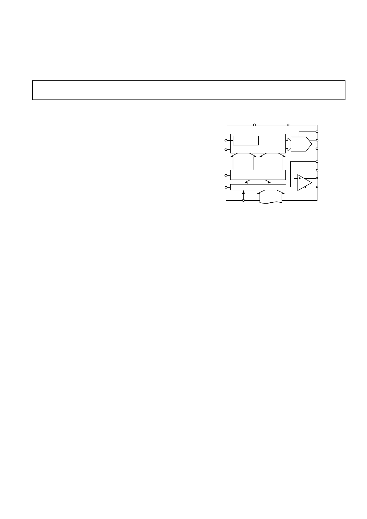
FUNCTIONAL BLOCK DIAGRAM
32-BIT
TUNING
WORD
PHASE
AND
CONTROL
WORDS
FREQUENCY/PHASE
DATA REGISTER
DATA INPUT REGISTER
10-BIT
DAC
DAC R
SET
ANALOG
OUT
ANALOG
IN
CLOCK OUT
CLOCK OUT
HIGH SPEED
DDS
FREQUENCY
UPDATE/DATA
REGISTER
RESET
WORD LOAD
CLOCK
MASTER
RESET
REF
CLOCK IN
63 REFCLK
MULTIPLIER
COMPARATOR
SERIAL
LOAD
1 BIT 3
40 LOADS
PARALLEL
LOAD
8 BITS 3
5 LOADS
FREQUENCY, PHASE
AND CONTROL DATA INPUT
AD9851
+V
S
GND
FEATURES
180 MHz Clock Rate with Selectable 6ⴛ Reference Clock
Multiplier
On-Chip High Performance 10-Bit DAC and High Speed
Comparator with Hysteresis
SFDR >43 dB @ 70 MHz A
OUT
32-Bit Frequency Tuning Word
Simplified Control Interface: Parallel or Serial
Asynchronous Loading Format
5-Bit Phase Modulation and Offset Capability
Comparator Jitter <80 ps p-p @ 20 MHz
+2.7 V to +5.25 V Single Supply Operation
Low Power: 555 mW @ 180 MHz
Power-Down Function, 4 mW @ +2.7 V
Ultrasmall 28-Lead SSOP Packaging
APPLICATIONS
Frequency/Phase-Agile Sine Wave Synthesis
Clock Recovery and Locking Circuitry for Digital
Communications
Digitally Controlled ADC Encode Generator
Agile L.O. Applications in Communications
Quadrature Oscillator
CW, AM, FM, FSK, MSK Mode Transmitter
GENERAL DESCRIPTION
The AD9851 is a highly integrated device that uses advanced
DDS technology, coupled with an internal high speed, high
performance D/A converter, and comparator, to form a digitallyprogrammable frequency synthesizer and clock generator function. When referenced to an accurate clock source, the AD9851
generates a stable frequency and phase-programmable digitized
analog output sine wave. This sine wave can be used directly as
a frequency source, or internally converted to a square wave for
agile-clock generator applications. The AD9851’s innovative
high speed DDS core accepts a 32-bit frequency tuning word,
which results in an output tuning resolution of approximately
0.04 Hz with a 180 MHz system clock. The AD9851 contains a
unique 6× REFCLK Multiplier circuit that eliminates the need
for a high speed reference oscillator. The 6× REFCLK Multiplier
has minimal impact on SFDR and phase noise characteristics.
The AD9851 provides five bits of programmable phase modulation resolution to enable phase shifting of its output in incre-
ments of 11.25°.
The AD9851 contains an internal high speed comparator that
can be configured to accept the (externally) filtered output of
the DAC to generate a low jitter output pulse.
The frequency tuning, control and phase modulation words are
asynchronously loaded into the AD9851 via parallel or serial
loading format. The parallel load format consists of five iterative loads of an 8-bit control word (byte). The first 8-bit byte
controls output phase, 6× REFCLK Multiplier, power-down
enable and loading format; the remaining bytes comprise the
32-bit frequency tuning word. Serial loading is accomplished
via a 40-bit serial data stream entering through one of the parallel
input bus lines. The AD9851 uses advanced CMOS technology
to provide this breakthrough level of functionality on just 555 mW
of power dissipation (+5 V supply), at the maximum clock rate of
180 MHz.
The AD9851 is available in a space-saving 28-lead SSOP, surface mount package that is pin-for-pin compatible with the
popular AD9850 125 MHz DDS. It is specified to operate over
the extended industrial temperature range of –40°C to +85°C at
>3.0 V supply voltage. Below 3.0 V, the specifications apply
over the commercial temperature range of 0°C to +85°C.
Page 2

–2– REV. C
AD9851–SPECIFICATIONS
Test AD9851BRS
P
arameter Temp Level Min Typ Max Units
CLOCK INPUT CHARACTERISTICS
Frequency Range (6× REFCLK Multiplier Disabled)
+5.0 V Supply FULL IV 1 180 MHz
+3.3 V Supply FULL IV 1 125 MHz
+2.7 V Supply 0°C to +85°C IV 1 100 MHz
Frequency Range (6× REFCLK Multiplier Enabled)
+5.0 V Supply FULL IV 5 30 MHz
+3.3 V Supply FULL IV 5 20.83 MHz
+2.7 V Supply 0°C to +85°C IV 5 16.66 MHz
Input Resistance +25°CV 1 MΩ
Minimum Switching Thresholds
2
Logic “1,” +5.0 V Supply +25°CIV3.5 V
Logic “1,” +3.3 V Supply +25°CIV2.3 V
Logic “0,” +5.0 V Supply +25°CIV 1.5V
Logic “0,” +3.3 V Supply +25°CIV 1 V
DAC OUTPUT CHARACTERISTICS
Full-Scale Output Current +25°C IV 5 10 20 mA
Gain Error +25°C I –10 10 % FS
Output Offset +25°CI 10µA
Differential Nonlinearity +25°C I 0.75 LSB
Integral Nonlinearity +25°C I 1 LSB
Residual Phase Noise, 5.2 MHz, 1 kHz Offset
PLL On +25°C V –125 dBc/Hz
PLL Off +25°C V –132 dBc/Hz
Output Impedance +25°C V 120 kΩ
Voltage Compliance Range +25°C I –0.5 1.5 V
Wideband Spurious-Free Dynamic Range
1.1 MHz Analog Out (DC to 72 MHz) +25°C IV 60 64 dBc
20.1 MHz Analog Out (DC to 72 MHz) +25°C IV 51 53 dBc
40.1 MHz Analog Out (DC to 72 MHz) +25°C IV 51 55 dBc
50.1 MHz Analog Out (DC to 72 MHz) +25°C IV 46 53 dBc
70.1 MHz Analog Out (DC to 72 MHz) +25°C IV 42 43 dBc
Narrowband Spurious-Free Dynamic Range
1.1 MHz (±50 kHz) +25°C V 85 dBc
1.1 MHz (±200 kHz) +25°C V 80 dBc
40.1 MHz (±50 kHz) +25°C V 85 dBc
40.1 MHz (±200 kHz) +25°C V 80 dBc
70.1 MHz (±50 kHz) +25°C V 85 dBc
70.1 MHz (±200 kHz) +25°C V 73 dBc
COMPARATOR INPUT CHARACTERISTICS
Input Capacitance +25°CV 3 pF
Input Resistance +25°C IV 500 kΩ
Input Bias Current +25°CI 12 µA
Input Voltage Range +25°CIV0 5 V
COMPARATOR OUTPUT CHARACTERISTICS
Logic “1” Voltage +5 V Supply +25°C VI +4.8 V
Logic “1” Voltage +3.3 V Supply +25°C VI +3.1 V
Logic “1” Voltage +2.7 V Supply +25°C VI +2.3 V
Logic “0” Voltage +25°C VI +0.4 V
Continuous Output Current +25°CIV 20mA
Hysteresis +25°CIV10 mV
Propagation Delay +25°CIV 7 ns
Toggle Frequency (1 V p-p Input Sine Wave) +25°C IV 200 MHz
Rise/Fall Time, 15 pF Output Load +25°CIV 7 ns
Output Jitter (p-p)
3
+25°C IV 80 ps (p-p)
CLOCK OUTPUT CHARACTERISTICS
Output Jitter (Clock Generator Configuration,
40 MHz 1 V p-p Input Sine Wave) +25°C V 250 ps (p-p)
Clock Output Duty Cycle FULL IV 50 ± 10 %
(V
S1
= +5 V ⴞ 5%, R
SET
= 3.9 k⍀, 6ⴛ REFCLK Multiplier Disabled, External Reference
Clock = 180 MHz except as noted)
Page 3

–3–REV. C
AD9851
Test AD9851BRS
Parameter Temp Level Min Typ Max Units
TIMING CHARACTERISTICS
4
tWH, tWL (W_CLK Min Pulsewidth High/Low) FULL IV 3.5 ns
t
DS
, tDH (Data to W_CLK Setup and Hold Times) FULL IV 3.5 ns
t
FH
, tFL (FQ_UD Min Pulsewidth High/Low) FULL IV 7 ns
t
CD
(REFCLK Delay After FQ_UD)
5
FULL IV 3.5 ns
t
FD
(FQ_UD Min Delay After W_CLK) FULL IV 7 ns
t
CF
(Output Latency from FQ_UD)
Frequency Change FULL IV 18 SYSCLK
Cycles
Phase Change FULL IV 13 SYSCLK
Cycles
t
RH
(CLKIN Delay After RESET Rising Edge) FULL IV 3.5 ns
t
RL
(RESET Falling Edge After CLKIN) FULL IV 3.5 ns
t
RR
(Recovery from RESET) FULL IV 2 SYSCLK
Cycles
t
RS
(Minimum RESET Width) FULL IV 5 SYSCLK
Cycles
t
OL
(RESET Output Latency) FULL IV 13 SYSCLK
Cycles
Wake-Up Time from Power-Down Mode
6
+25°CV 5 µs
CMOS LOGIC INPUTS
Logic “1” Voltage, +5 V Supply +25°CI 3.5 V
Logic “1” Voltage, +3.3 V Supply +25°CI 3.0 V
Logic “1” Voltage, +2.7 V Supply +25°CI 2.4 V
Logic “0” Voltage +25°CI 0.4 V
Logic “1” Current +25°CI 12 µA
Logic “0” Current +25°CI 12 µA
Rise/Fall Time +25°C IV 100 ns
Input Capacitance +25°CV 3 pF
POWER SUPPLY
V
S
6
Current @:
62.5 MHz Clock, +2.7 V Supply +25°CVI 3035mA
100 MHz Clock, +2.7 V Supply +25°CVI 4050mA
62.5 MHz Clock, +3.3 V Supply +25°CVI 3545mA
125 MHz Clock, +3.3 V Supply +25°CVI 5570mA
62.5 MHz Clock, +5 V Supply +25°CVI 5065mA
125 MHz Clock, +5 V Supply +25°CVI 7090mA
180 MHz Clock, +5 V Supply +25°C VI 110 130 mA
Power Dissipation @ :
62.5 MHz Clock, +5 V Supply +25°C VI 250 325 mW
62.5 MHz Clock, +3.3 V Supply +25°C VI 115 150 mW
62.5 MHz Clock, +2.7 V Supply +25°CVI 8595mW
100 MHz Clock, +2.7 V Supply +25°C VI 110 135 mW
125 MHz Clock, +5 V Supply +25°C VI 365 450 mW
125 MHz Clock, +3.3 V Supply +25°C VI 180 230 mW
180 MHz Clock, +5 V Supply +25°C VI 555 650 mW
P
DISS
Power-Down Mode @:
+5 V Supply +25°CVI 1755mW
+2.7 V Supply +25°CVI 4 20 mW
NOTES
1
+VS collectively refers to the positive voltages applied to DVDD, PVCC and AVDD. Voltages applied to these pins should be of the same potential.
2
Indicates the minimum signal levels required to reliably clock the device at the indicated supply voltages. This specifies the p-p signal level and dc offset needed when
the clocking signal is not of CMOS/TTL origin, i.e., a sine wave with 0 V dc offset.
3
The comparator’s jitter contribution to any input signal. This is the minimum jitter on the outputs that can be expected from an ideal input. Considerably more
output jitter is seen when nonideal input signals are presented to the comparator inputs. Nonideal characteristics include the presence of extraneous, nonharmonic
signals (spur’s, noise), slower slew rate and low comparator overdrive.
4
Timing of input signals FQ_UD, WCLK, RESET are asynchronous to the Reference Clock; however, the presence of a Reference Clock is required to implement
those functions. In the absence of a Reference Clock, the AD9851 automatically enters power-down mode rendering the IC, including the comparator, inoperable
until a Reference Clock is restored. Very high speed updates of frequency/phase word will require FQ_UD and WCLK to be externally synchronized with the external Reference Clock to assure proper timing.
5
Not applicable when 6× REFCLK Multiplier is engaged.
6
Assumes no capacitive load on DACBP (Pin 17).
Specifications subject to change without notice.
Page 4
AD9851
–4– REV. C
CAUTION
ESD (electrostatic discharge) sensitive device. Electrostatic charges as high as 4000 V readily
accumulate on the human body and test equipment and can discharge without detection.
Although the AD9851 features proprietary ESD protection circuitry, permanent damage may
occur on devices subjected to high energy electrostatic discharges. Therefore, proper ESD
precautions are recommended to avoid performance degradation or loss of functionality.
Application Note: Users are cautioned not to apply digital input signals prior to power-up of this
device. Doing so may result in a latch-up condition.
WARNING!
ESD SENSITIVE DEVICE
ABSOLUTE MAXIMUM RATINGS*
Maximum Junction Temperature . . . . . . . . . . . . . . . .+150°C
Storage Temperature . . . . . . . . . . . . . . . . . . –65°C to +150°C
V
S
. . . . . . . . . . . . . . . . . . . . . . . . . . . . . . . . . . . . . . . . . . +6 V
Operating Temperature . . . . . . . . . . . . . . . . . –40°C to +85°C
Digital Inputs . . . . . . . . . . . . . . . . . . . –0.7 V to +V
S
+ 0.7 V
Lead Temperature (10 sec) Soldering . . . . . . . . . . . . .+300°C
Digital Output Current . . . . . . . . . . . . . . . . . . . . . . . . 30 mA
SSOP θ
JA
Thermal Impedance . . . . . . . . . . . . . . . . . . 82°C/W
DAC Output Current . . . . . . . . . . . . . . . . . . . . . . . . . .30 mA
*Absolute maximum ratings are limiting values, to be applied individually, and
beyond which the serviceability of the circuit may be impaired. Functional
operability under any of these conditions is not necessarily implied. Exposure of
absolute maximum rating conditions for extended periods of time may affect
device reliability.
EXPLANATION OF TEST LEVELS
Test Level
I – 100% Production Tested.
III – Sample Tested Only.
IV – Parameter is guaranteed by design and characterization
testing.
V – Parameter is a typical value only.
VI – Devices are 100% production tested at +25°C and
guaranteed by design and characterization testing for
industrial operating temperature range.
ORDERING GUIDE
Model Temperature Range Package Description Package Option
AD9851BRS –40°C to +85°C Shrink Small Outline (SSOP) RS-28
Page 5
AD9851
–5–REV. C
PIN FUNCTION DESCRIPTIONS
Pin
No. Mnemonic Function
4–1, D0–D7 8-Bit Data Input. The data port for loading the 32-bit frequency and 8-bit phase/control words. D7 = MSB;
28–25 D0 = LSB. D7, Pin 25, also serves as the input pin for 40-bit serial data word.
5 PGND 6× REFCLK Multiplier Ground Connection.
6 PVCC 6× REFCLK Multiplier Positive Supply Voltage Pin.
7 W_CLK Word Load Clock. Rising edge loads the parallel or serial frequency/phase/control words asynchronously
into the 40-bit input register.
8 FQ_UD Frequency Update. A rising edge asynchronously transfers the contents of the 40-bit input register to be
acted upon by the DDS core. FQ_UD should be issued when the contents of the input register are known
to contain only valid, allowable data.
9 REFCLOCK Reference Clock Input. CMOS/TTL-level pulse train, direct or via the 6× REFCLK Multiplier. In direct
mode, this is also the SYSTEM CLOCK. If the 6× REFCLK Multiplier is engaged, then the output of the
multiplier is the SYSTEM CLOCK. The rising edge of the SYSTEM CLOCK initiates operations.
10, 19 AGND Analog Ground. The ground return for the analog circuitry (DAC and Comparator).
11, 18 AVDD Positive supply voltage for analog circuitry (DAC and Comparator, Pin 18) and bandgap voltage reference,
Pin 11.
12 R
SET
The DAC’s external R
SET
connection—nominally a 3.92 kΩ resistor to ground for 10 mA out. This sets
the DAC full-scale output current available from IOUT and IOUTB. R
SET
= 39.93/IOUT
13 VOUTN Voltage Output Negative. The comparator’s “complementary” CMOS logic level output.
14 VOUTP Voltage Output Positive. The comparator’s “true” CMOS logic level output.
15 VINN Voltage Input Negative. The comparator’s inverting input.
16 VINP Voltage Input Positive. The comparator’s noninverting input.
17 DACBP DAC Bypass Connection. This is the DAC voltage reference bypass connection normally NC (NO
CONNECT) for optimum SFDR performance.
20 IOUTB The “complementary” DAC output with same characteristics as IOUT except that IOUTB = (full-scale
output–IOUT). Output load should equal that of IOUT for best SFDR performance.
21 IOUT The “true” output of the balanced DAC. Current is “sourcing” and requires current-to-voltage
conversion, usually a resistor or transformer referenced to GND. IOUT = (full-scale output–IOUTB)
22 RESET Master Reset pin; active high; clears DDS accumulator and phase offset register to achieve 0 Hz and 0°
output phase. Sets programming to parallel mode and disengages the 6× REFCLK Multiplier. Reset does
not clear the 40-bit input register. On power-up, asserting RESET should be the first priority before pro-
gramming commences.
23 DVDD Positive supply voltage pin for digital circuitry.
24 DGND Digital Ground. The ground return pin for the digital circuitry.
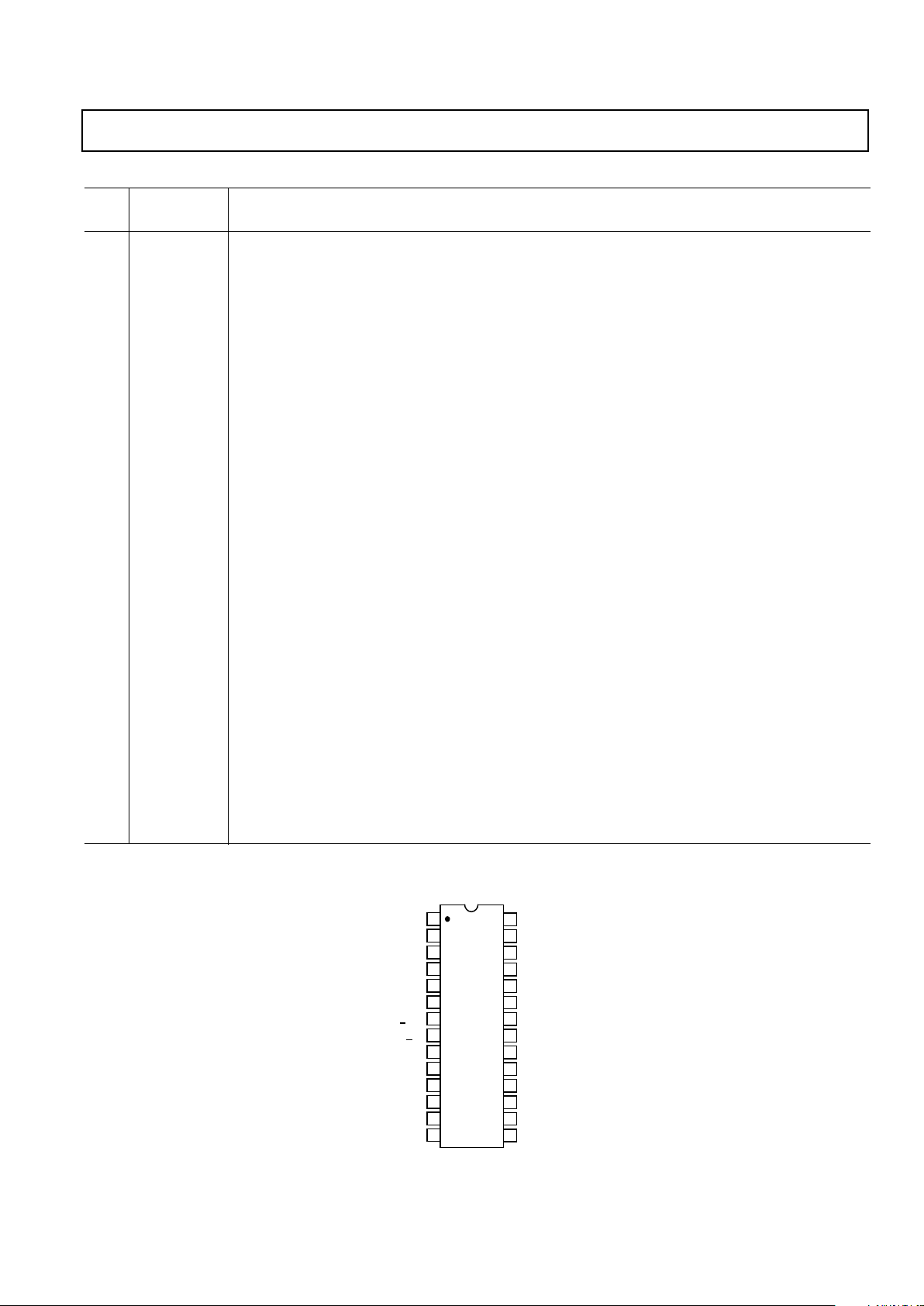
PIN CONFIGURATION
TOP VIEW
(Not to Scale)
28
27
26
25
24
23
22
21
20
19
18
17
16
15
1
2
3
4
5
6
7
8
9
10
11
12
13
14
AD9851
VOUTP
VOUTN
R
SET
AVDD
AGND
REFCLOCK
FQ UD
D3
D2
D1
LSB D0
PVCC
PGND
VINN
VINP
DACBP
AVDD
AGND
IOUTB
IOUT
D4
D5
D6
D7 MSB/SERIAL LOAD
RESET
DVDD
DGND
W
CLK
Page 6
AD9851
–6– REV. C
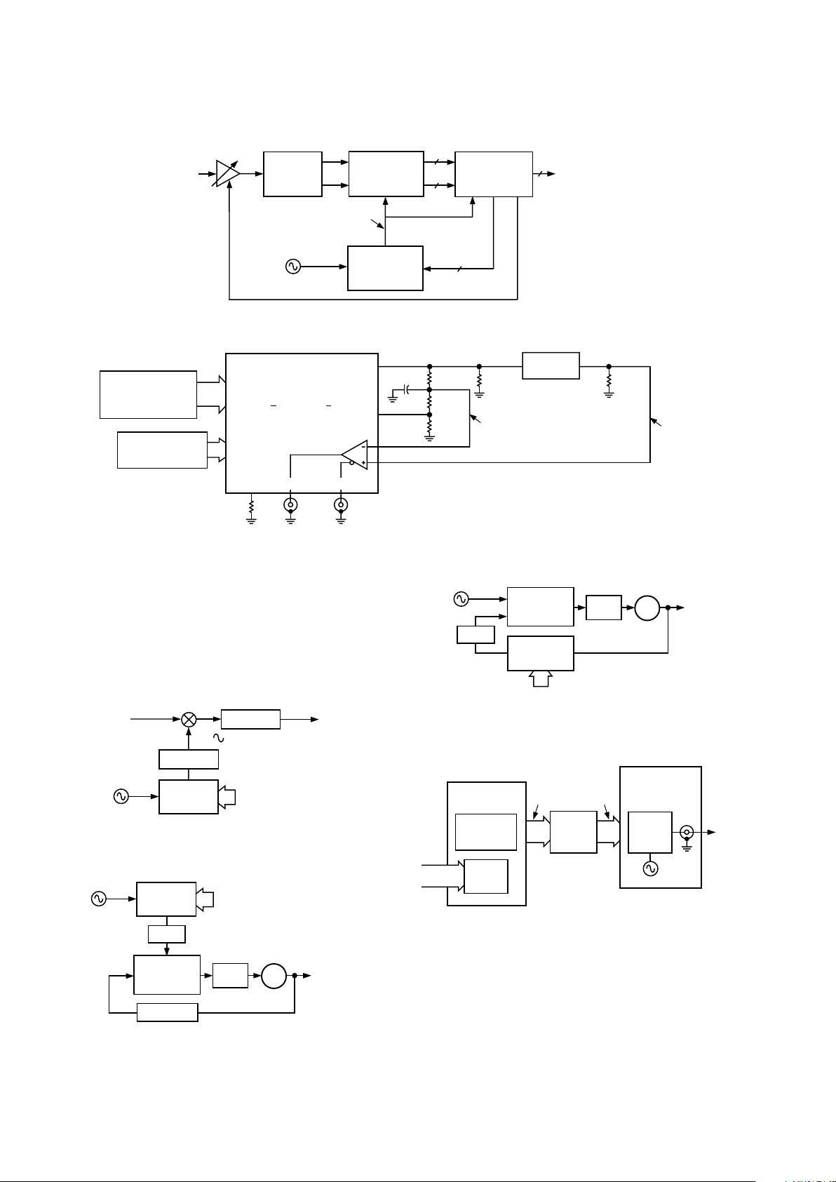
Both IOUT and IOUTB are equally loaded with 100 Ω. Two
100 kΩ resistors “sample” each output and average the two
voltages. The result is filtered with the 470 pF capacitor and
applied to one comparator input as a dc switching threshold.
The filtered DAC sine wave output is applied to the other comparator input. The comparator will toggle with nearly 50% duty
cycle as the sine wave alternately traverses the “center point”
threshold.
AD9851
DDS
REFERENCE
CLOCK
IF FREQUENCY
IN
FILTER
FILTER
TUNING
WORD
RF
FREQUENCY
OUT
Figure 3. Frequency/Phase-Agile Local Oscillator for
Frequency Mixing/Multiplying
FILTER
PHASE
COMPARATOR
DIVIDE-BY-N
LOOP
FILTER
VCO
AD9851
DDS
REFERENCE
CLOCK
TUNING
WORD
RF
FREQUENCY
OUT
Figure 4. Frequency/Phase-Agile Reference for PLL
I/Q MIXER
AND
LOW PASS
FILTER
I
Q
AD9059
DUAL
8-BIT ADC
8
8
DIGITAL
DEMODULATOR
ADC ENCODE
AGC
32
CHIP/SYMBOL/PN
RATE DATA
ADC CLOCK FREQUENCY
LOCKED TO
Tx CHIP/SYMBOL/PN RATE
180MHz
OR 30MHz
REFERENCE
CLOCK
Rx BASEBAND
DIGITAL DATA OUT
Rx
RF IN
VCA
AD9851
CLOCK
GENERATOR
Figure 1. “Chip Rate” Clock Generator Application in a Spread Spectrum Receiver
MICROPROCESSOR
OR
MICROCONTROLLER
DATA
BUS
180MHz OR 30MHz
REFERENCE
CLOCK
8-BIT PARALLEL DATA,
OR 1-BIT 3 40 SERIAL DATA,
RESET, W CLK AND FQ UD
IOUT
100kV
100kV
470pF
100V
IOUTB
R
SET
3.9kV
CMOS
OUTPUTS
QOUTBQOUT
LOW-PASS
FILTER
7TH ORDER ELLIPTICAL
70MHz LOW PASS
200V IMPEDANCE
200V
VOLTAGE HERE = CENTER POINT
OF SINE WAVE (0.5V TYPICALLY)
USING PASSIVE "AVERAGING" CIRCUIT
0 TO 1V p-p
SINE WAVE
AD9851
200V
Figure 2. Basic Clock Generator Configuration
PHASE
COMPARATOR
LOOP
FILTER
VCO
AD9851
DDS
REFERENCE
CLOCK
TUNING
WORD
RF
FREQUENCY
OUT
FILTER
REF CLK IN
PROGRAMMABLE
"DIVIDE-BY-N" FUNCTION
(WHERE N = 2
32
/TUNING WORD)
Figure 5. Digitally-Programmable “Divide-by-N” Function
in PLL
AD9851
DDS
FM RF
OUTPUT
ADSP-2181
DSP
PROCESSOR
ADSP-2181
BUS
INPUT/
OUTPUT
DECODE
LOGIC
8-BIT
DATA
BUS
AD1847
STEREO
CODEC
L & R
AUDIO IN
REF
OSC
DAC
OUT
AD9851/FSPCB
EVALUATION
BOARD
EZ-KIT LITE
DSP
Figure 6. High Quality, All-Digital RF Frequency Modulation
High quality, all digital RF frequency modulation generation
with the ADSP-2181 DSP and the AD9851 DDS. This application is well documented in Analog Devices’ application Note
AN-543, and uses an “image” of the DDS output as illustrated
in Figure 8.
Page 7
AD9851
–7–REV. C
REF
CLOCK
90
PHASE
DIFFERENCE
8-BIT DATA BUS
FQ UD
RESET
W CLK
AD9851
#2
IOUT
AD9851
#1
W CLK
FQ UD
RESET
IOUT
RESET
FQ
UD
RESET
FQ
UD
W
CLK #2
W CLK #1
MICROPROCESSOR
OR
MICROCONTROLLER
W
CLK #2
W
CLK #1
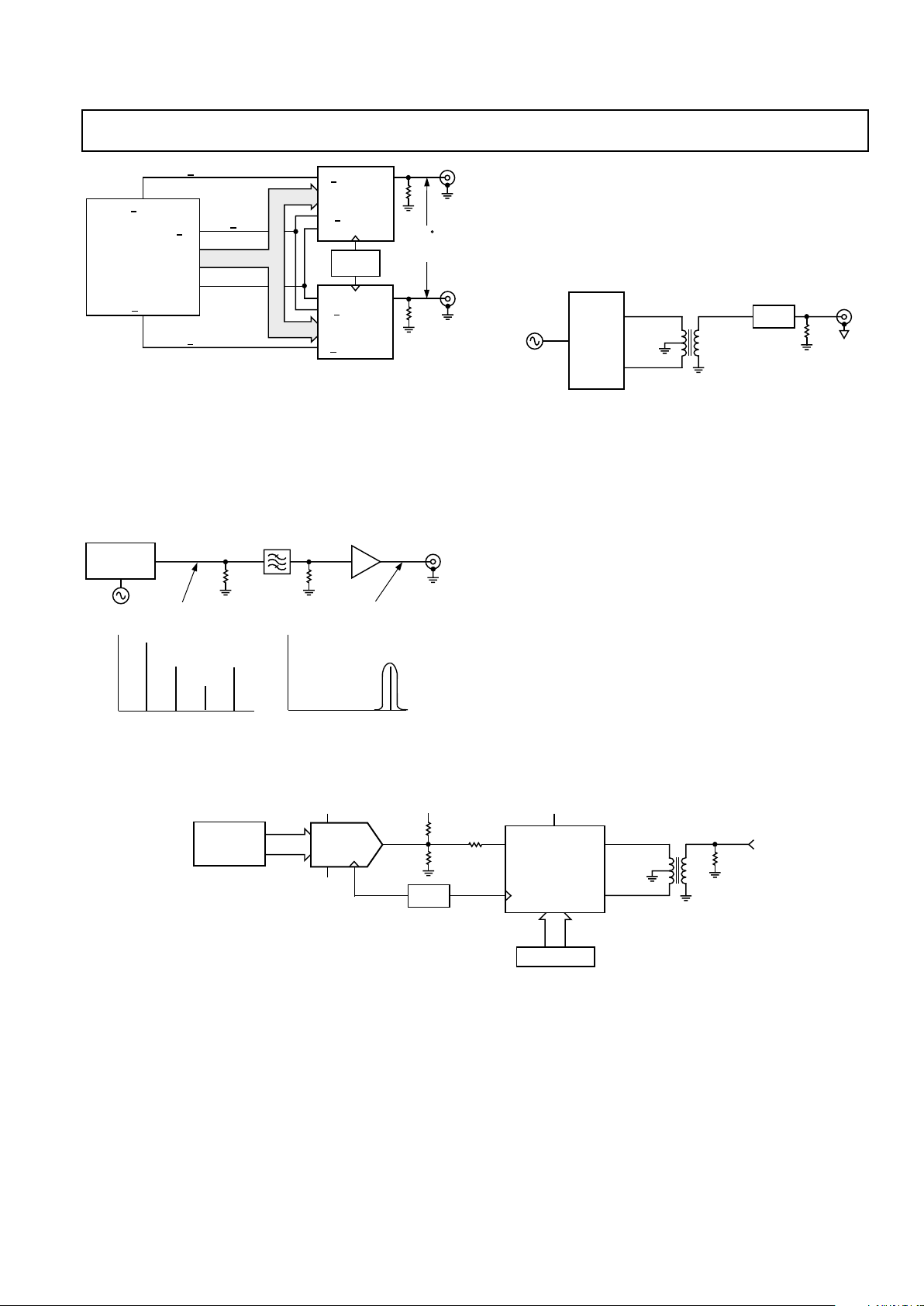
Figure 7. Application Showing Synchronization of Two
AD9851 DDSs to Form a Quadrature Oscillator
After a common RESET command is issued, separate W_CLKs
allow independent programming of each AD9851 40-bit input
register via the 8-bit data bus or serial input pin. A common
FQ_UD pulse is issued after programming is completed to
simultaneously engage both oscillators at their specified frequency and phase.
AD9851
IOUT
30MHz
CLOCK
BANDPASS
FILTER
50V
50V
FUNDAMENTAL
F
CLK
IMAGE
F
C
– F
O
IMAGE
F
C
+ F
O
AMPLITUDE
60 120 180 240
FREQUENCY – MHz
240
FREQUENCY – MHz
IMAGE
F
C
+ F
O
BANDPASS
FILTER
AMPLITUDE
3 6
AMPLIFIER
240MHz
AD9851
SPECTRUM
FINAL OUTPUT
SPECTRUM
Figure 8. Deriving a High Frequency Output Signal from
the AD9851 by Using an “Alias” or Image Signal
Differential DAC output connection (Figure 9) for reduction of
common-mode signals and to allow highly reactive filters to be
driven without a filter input termination resistor (see above
single-ended example, Figure 8). A 6 dB power advantage is
obtained at the filter output as compared with the single-ended
example, since the filter need not be doubly terminated.
REFERENCE
CLOCK
FILTER
DIFFERENTIAL
TRANSFORMER-COUPLED
OUTPUT
50V
1:1 TRANSFORMER
i.e., MINI-CIRCUITS T1–1T
50V
AD9851
DDS
21
20
Figure 9. Differential DAC Output Connection for Reduction of Common-Mode Signals
The AD9851 R
SET
input being driven by an external DAC
(Figure 10) to provide amplitude modulation or fixed, digital
amplitude control of the DAC output current. Full description
of this application is found as a “Technical Note” on the AD9851
web page (site address is www.analog.com) under “Related
Information.” An Analog Devices application note for the
AD9850, AN-423, describes another method of amplitude
control using an enhancement-mode MOSFET that is equally
applicable to the AD9851.
NOTE: If the 6× REFCLK Multiplier of the AD9851 is en-
gaged, the 125 MHz clocking source shown in Figure 10 can be
reduced by a factor of six.
AD9851
DDS
DIFFERENTIAL
TRANSFORMER-COUPLED
OUTPUT
50V
1:1 TRANSFORMER
50V
IOUT
IOUT
R
SET
+5V
21
20
12
9
4kV
200V
330V
+5V
20mA
MAX
10-BIT DAC
AD9731
+5V
–5V
125MHz
10 BITS
DATA
GENERATOR
e.g., DG-2020
COMPUTER
CONTROL
DATA
Figure 10. The AD9851 R
SET
Input Being Driven by an External DAC
Page 8

AD9851
–8– REV. C
THEORY OF OPERATION AND APPLICATION
The AD9851 uses direct digital synthesis (DDS) technology, in
the form of a numerically-controlled oscillator (NCO), to generate a frequency/phase-agile sine wave. The digital sine wave is
converted to analog form via an internal 10-bit high speed D/A
converter. An on-board high-speed comparator is provided to
translate the analog sine wave into a low-jitter TTL/CMOScompatible output square wave. DDS technology is an innovative circuit architecture that allows fast and precise manipulation
of its output word, under full digital control. DDS also enables
very high resolution in the incremental selection of output frequency. The AD9851 allows an output frequency resolution of
approximately 0.04 Hz at 180 MSPS clock rate with the option of
directly using the reference clock or by engaging the 6× REFCLK
Multiplier. The AD9851’s output waveform is phase-continuous from one output frequency change to another.
The basic functional block diagram and signal flow of the
AD9851 configured as a clock generator is shown in Figure 11.
The DDS circuitry is basically a digital frequency divider function whose incremental resolution is determined by the frequency
of the system clock, and N (number of bits in the tuning word).
The phase accumulator is a variable-modulus counter that
increments the number stored in it each time it receives a clock
pulse. When the counter reaches full scale it “wraps around,”
making the phase accumulator’s output phase-continuous. The
frequency tuning word sets the modulus of the counter, which
effectively determines the size of the increment (∆ Phase) that
will be added to the value in the phase accumulator on the next
clock pulse. The larger the added increment, the faster the
accumulator wraps around, which results in a higher output
frequency.
The AD9851 uses an innovative and proprietary “Angle
Rotation” algorithm that mathematically converts the 14-bit
truncated value of the 32-bit phase accumulator to the 10-bit
quantized amplitude that is passed to the DAC. This unique
algorithm uses a much-reduced ROM look-up table and DSP to
perform this function. This contributes to the small size and
low power dissipation of the AD9851.
The relationship between the output frequency, system clock
and tuning word of the AD9851 is determined by the expression:
f
OUT
= (∆ Phase × System Clock)/2
32
where:
∆Phase = decimal value of 32-bit frequency tuning word.
System Clock = direct input reference clock (in MHz) or 6× the
input clock (in MHz) if the 6× REFCLK Multiplier is engaged.
f
OUT
= frequency of the output signal in MHz.
The digital sine wave output of the DDS core drives the internal
high-speed 10-bit D/A converter that will construct the sine
wave in analog form. This DAC has been optimized for dynamic
performance and low glitch energy, which results in the low
spurious and jitter performance of the AD9851. The DAC can
be operated in either the single-ended, Figures 2 and 8, or differential output configuration, Figures 9 and 10. DAC output
current and R
SET
values are determined using the following
expressions:
I
OUT
= 39.93/R
SET
R
SET
= 39.93/I
OUT
Since the output of the AD9851 is a sampled signal, its output
spectrum follows the Nyquist sampling theorem. Specifically, its
output spectrum contains the fundamental plus aliased signals
(images) that occur at integer multiples of the system clock
frequency ± the selected output frequency. A graphical repre-
sentation of the sampled spectrum, with aliased images, is shown in
Figure 12. Normal usable bandwidth is considered to extend
from dc to 1/2 the system clock.
In the example shown in Figure 12, the system clock is 100 MHz
and the output frequency is set to 20 MHz. As can be seen, the
aliased images are very prominent and of a relatively high energy
CLOCK
OUT
AMPLITUDE/SINE
CONV ALGORITHM
PHASE
ACCUMULATOR
DDS CIRCUITRY
D/A
CONVERTER
LP COMPARATOR
N
REFERENCE
CLOCK
TUNING WORD SPECIFIES
OUTPUT FREQUENCY AS A
FRACTION OF REF CLOCK
FREQUENCY
IN DIGITAL
DOMAIN
Figure 11. Basic DDS Block Diagram and Signal Flow of AD9851
120MHz
2ND IMAGE
F
OUT
FC+F
O
2FC–F
O
2FC+F
O
3FC–F
O
180MHz
3RD IMAGE
220MHz
4TH IMAGE
280MHz
5TH IMAGE
80MHz
1ST IMAGE
20MHz0Hz
(DC)
F
C
FC–F
O
SIN (X)/3 ENVELOPE
3 = (p)F/F
C
100MHz
SYSTEM CLOCK FREQUENCY
SIGNAL AMPLITUDE
Figure 12. Output Spectrum of a Sampled Sin(X)/X Signal
Page 9

AD9851
–9–REV. C
level as determined by the sin(x)/x roll-off of the quantized D/A
converter output. In fact, depending on the f/system clock relationship, the 1st aliased image can equal the fundamental
amplitude (when f
OUT
= 1/2 system clock). A low-pass filter is
generally placed between the output of the D/A converter and
the input of the comparator to suppress the jitter-producing
effects of non-harmonically related aliased images and other
spurious signals. Consideration must be given to the relationship
of the selected output frequency, the system clock frequency and
alias frequencies to avoid unwanted output anomalies.
Images need not be thought of as useless by-products of a DAC.
In fact, with bandpass filtering around an image and some
amount of post-filter amplification, the image can become the
primary output signal (see Figure 8). Since images are not har-
monics, they retain a 1:1 ∆frequency relationship to the funda-
mental output. That is, if the fundamental is shifted 1 kHz, then
the image is also shifted 1 kHz. This relationship accounts for
the frequency stability of an image, which is identical to that of
the fundamental. Users should recognize that the lower image of
an image pair surrounding an integer multiple of the system clock
will move in a direction opposite the fundamental. Images of an
image pair located above an integer multiple of the system clock
will move in the same direction as a fundamental movement.
The frequency band where images exist is much richer in spurious signals and therefore, more hostile in terms of SFDR. Users
of this technique should empirically determine what frequencies
are usable if their SFDR requirements are demanding.
A good “rule-of-thumb” for applying the AD9851 as a clock
generator is to limit the fundamental output frequency to 40% of
Reference Clock frequency to avoid generating aliased signals
that are too close to the output band of interest (generally dc—
highest selected output frequency) to be filtered. This practice
will ease the complexity and cost of the external filter requirement for the clock generator application.
The reference clock input of the AD9851 has minimum limita-
tion of 1 MHz without 6× REFCLK Multiplier engaged and
5 MHz with multiplier engaged. The device has internal circuitry that senses when the clock rate has dropped below the
minimum and automatically places itself in the power-down
mode. In this mode, the on-chip comparator is also disabled.
This is important information for those who may wish to use the
on-chip comparator for purposes other than squaring the DDS
sine wave output. When the clock frequency returns above the
minimum threshold, the device resumes normal operation after
5 µs (typically). This shutdown mode prevents excessive current
leakage in the dynamic registers of the device.
The impact of reference clock phase noise in DDS systems is
actually reduced, since the DDS output is the result of a division
of the input frequency. The amount of apparent phase noise
reduction, expressed in dB, is found using: 20 log f
OUT/fCLK
.
Where f
OUT
is the fundamental DDS output frequency and f
CLK
is the system clock frequency. From this standpoint, using the
highest system clock input frequency makes good sense in reducing the effects of reference clock phase noise contribution to the
output signals’ overall phase noise. As an example, an oscillator with –100 dBc phase noise operating at 180 MHz would
appear as a –125 dB contribution to DDS overall phase noise for
a 10 MHz output. Engaging the 6× REFCLK Multiplier has
generally been found to increase overall output phase noise. This
increase is due to the inherent 6× (15.5 dB) phase gain transfer
function of the 6× REFCLK Multiplier, as well as noise gener-
ated internally by the clock multiplier circuit. By using a low
phase noise reference clock input to the AD9851, users can be
assured of better than –100 dBc/Hz phase noise performance
for output frequencies up to 50 MHz at offsets from 1 kHz to
100 kHz.
Programming the AD9851
The AD9851 contains a 40-bit register that stores the 32-bit
frequency control word, the 5-bit phase modulation word,
6× REFCLK Multiplier enable and the power-down function.
This register can be loaded in parallel or serial mode. A logic
high engages functions; for example, to power-down the IC
(sleep mode), a logic high must be programmed in that bit
location. Those users who are familiar with the AD9850 DDS
will find only a slight change in programming the AD9851,
specifically, data[0] of W0 (parallel load) and W32 (serial load)
now contains a “6× REFCLK Multiplier Enable” bit that needs
to be set high to enable or low to disable the internal reference
clock multiplier.
Note: setting “data[1]” high in programming word W0 (parallel mode) or word W33 high in serial mode is not allowed (see
Tables I and III). This bit controls a “factory test mode” that
will cause abnormal operation in the AD9851 if set high. If
erroneously entered (as evidenced by Pin 2 changing from an
input pin to an output signal), an exit is provided by asserting
RESET. Unintentional entry to the factory test mode can
occur if an FQ_UD pulse is sent after initial power-up and
RESET of the AD9851. Since RESET does not clear the 40bit input register, this will transfer the random power-up values
of the input register to the DDS core. The random values may
invoke the factory test mode or power-down mode. Never issue
an FQ_UD command if the 40-bit input register contents are
unknown.
In the default parallel load mode, the 40-bit input register is
loaded using an 8-bit bus. W_CLK is used to load the register
in five iterations of eight bytes. The rising edge of FQ_UD
transfers the contents of the register into the device to be acted
upon and resets the word address pointer to W0. Subsequent
W_CLK rising edges load 8-bit data, starting at W0 and then
move the word pointer to the next word. After W0 through W4
are loaded, additional W_CLK edges are ignored until either a
RESET is asserted or an FQ_UD rising edge resets the address
pointer to W0 in preparation for the next 8-bit load. See Figure 13.
In serial load mode, forty subsequent rising edges of W_CLK
will shift and load the 1-bit data on Pin 25 (D7) through the
40-bit register in “shift-register” fashion. Any further W_CLK
rising edges after the register is full will shift data out causing
data that is left in the register to be out-of-sequence and corrupted. The serial mode must be entered from the default
parallel mode, see Figure 17. Data is loaded beginning with
W0 and ending with W39. One note of caution: the 8-bit
parallel word (W0)—xxxxx011—that invokes the serial mode
should be overwritten with a valid 40-bit serial word immediately after entering the serial mode to prevent unintended
engaging of the 6× REFCLK Multiplier or entry into the fac-
tory test mode. Exit from serial mode to parallel mode is only
possible using the RESET command.
Page 10

AD9851
–10– REV. C
Table I. 8-Bit Parallel-Load Data/Control Word Functional Assignment
Word Data[7] Data[6] Data[5] Data[4] Data[3] Data[2] Data[1] Data[0]
W0 Phase–b4 (MSB) Phase–b3 Phase–b2 Phase–b1 Phase–b0 (LSB) Power-Down Logic 0*
6× REFCLK
Multiplier
Enable
W1 Freq–b31 (MSB) Freq–b30 Freq–b29 Freq–b28 Freq–b27 Freq–b26 Freq–b25 Freq–b24
W2 Freq–b23 Freq–b22 Freq–b21 Freq–b20 Freq–b19 Freq–b18 Freq–b17 Freq–b16
W3 Freq–b15 Freq–b14 Freq–b13 Freq–b12 Freq–b11 Freq–b10 Freq–b9 Freq–b8
W4 Freq–b7 Freq–b6 Freq–b5 Freq–b4 Freq–b3 Freq–b2 Freq–b1 Freq–b0 (LSB)
*This bit is always Logic 0 unless invoking the serial mode (see Figure 17). After serial mode is entered, this data bit must be set back to Logic 0 for proper operation.
W0* W1 W2 W3 W4
t
CD
t
DH
t
DS
t
WL
t
WH
t
FD
t
FH
t
FL
*OUTPUT UPDATE CAN OCCUR AFTER ANY WORD LOAD
AND IS ASYNCHRONOUS WITH REFERENCE CLOCK
t
CF
VALID DATA
SYSCLK
DATA
W
CLK
FQ UD
A
OUT
Figure 13. Parallel-Load Frequency/Phase Update Timing Sequence
Note: To update W0 it is not necessary to load W1 through W4. Simply load W0 and assert FQ_UD. To update W1, reload W0
then W1 . . . users do not have random access to programming words.
Table II. Timing Specifications
Symbol Definition Min
t
DS
Data Setup Time 3.5 ns
t
DH
Data Hold Time 3.5 ns
t
WH
W_CLK High 3.5 ns
t
WL
W_CLK Low 3.5 ns
t
CD
REFCLK Delay after FQ_UD 3.5 ns*
t
FH
FQ_UD High 7.0 ns
t
FL
FQ_UD Low 7.0 ns
t
FD
FQ_UD Delay after W_CLK 7.0 ns
t
CF
Output Latency from FQ_UD
Frequency Change 18 SYSCLK Cycles
Phase Change 13 SYSCLK Cycles
*Specification does not apply when the 6× REFCLK Multiplier is engaged.
The function assignments of the data and control words are
shown in Tables I and III; the detailed timing sequence for
updating the output frequency and/or phase, resetting the de-
vice, engaging the 6× REFCLK Multiplier, and powering up/
down, are shown in the timing diagrams of Figures 13–20. As a
programming example for the following DDS characteristics:
1. Phase set to 11.25 degrees.
2. 6× REFCLK Multiplier engaged.
3. Powered-up mode selected.
4. Output = 10 MHz (for 180 MHz system clock).
In parallel mode, user would program the 40-bit control word
(composed of five 8-bit loads) as follows:
W0 = 00001001
W1 = 00001110
W2 = 00111000
W3 = 11100011
W4 = 10001110
If in serial mode, load the 40 bits starting from the LSB location
of W4 in the above “array,” loading from right to left, and ending with the MSB of W0.
Page 11

AD9851
–11–REV. C
Results of Reset, Figure 14
– Phase Accumulator zeroed such that the output = 0 Hertz
(dc).
– Phase Offset register set to zero such that DAC IOUT = Full-
Scale output and IOUTB = zero mA output.
– Internal Programming Address pointer reset to W0.
– Power-down bit reset to “0” (power-down disabled).
– 40-bit Data Input Register is NOT cleared.
–6× Reference Clock multiplier is disabled.
– Parallel programming mode selected by default.
XXXXX10X
FQ UD
W
CLK
SYSCLK
DAC
STROBE
DATA (W0)
INTERNAL CLOCKS
DISABLED
Figure 15. Parallel-Load Power-Down Sequence/Internal
Operation
XXXXX00X
FQ UD
W
CLK
DATA (W0)
INTERNAL CLOCKS
ENABLED
SYSCLK
Figure 16. Parallel-Load Power-Up Sequence (to Recover
from Power-Down)/Internal Operation
SYSCLK
RESET
A
OUT
t
RS
t
RH
t
RL
t
OL
COS (08)
SYMBOL DEFINITION MIN SPEC
t
RH
CLK DELAY AFTER RESET RISING EDGE 3.5ns*
t
RL
RESET FALLING EDGE AFTER CLK 3.5ns*
t
RR
RECOVERY FROM RESET 2 SYSCLK CYCLES
t
RS
MINIMUM RESET WIDTH 5 SYSCLK CYCLES
t
OL
RESET OUTPUT LATENCY 13 SYSCLK CYCLES
*SPECIFICATIONS DO NOT APPLY WHEN THE REF CLOCK MULTIPLIER IS ENGAGED
t
RR
Figure 14. Master Reset Timing Sequence
Entry to the serial mode, Figure 17, is via the parallel mode
which is selected by default after a RESET is asserted. One
needs only to program the first eight bits (word W0) with the
sequence xxxxx011 as shown in Figure 17 to change from parallel to serial mode. The W0 programming word may be sent over
the 8-bit data bus or hardwired as shown in Figure 18. After
serial mode is achieved, the user must follow the programming
sequence of Figure 19.
XXXXX011
FQ UD
W
CLK
DATA (W0)
ENABLE
SERIAL MODE
Figure 17. Serial-Load Enable Sequence
Note: After serial mode is invoked, it is best to immediately
write a valid 40-bit serial word (see Figure 19), even if it is all
zeros, followed by a FQ_UD rising edge to flush the “residual”
data left in the DDS core. A valid 40-bit serial word is any word
where W33 is Logic 0.
28
27
26
25
1
2
3
4
AD9851
D3
D2
D1
D0
D4
D5
D6
D7
10kV
+V
SUPPLY
Figure 18. Hardwired xxxxx011 Configuration for SerialLoad Enable Word W0 in Figure 17
Page 12

AD9851
–12– REV. C
FQ UD
W2
DATA
40 W CLK CYCLES
W CLK
W1 W3
W39
W0
Figure 19. Serial-Load Frequency/Phase Update Sequence
Table III. 40-Bit Serial-Load Word Functional Assignment
W0 Freq–b0 (LSB)
W1 Freq–b1
W2 Freq–b2
W3 Freq–b3
W4 Freq–b4
W5 Freq–b5
W6 Freq–b6
W7 Freq–b7
W8 Freq–b8
W9 Freq–b9
W10 Freq–b10
W11 Freq–b11
W12 Freq–b12
W13 Freq–b13
W14 Freq–b14
W15 Freq–b15
W16 Freq–b16
W17 Freq–b17
W18 Freq–b18
W19 Freq–b19
W20 Freq–b20
W21 Freq–b21
W22 Freq–b22
W23 Freq–b23
W24 Freq–b24
W25 Freq–b25
W26 Freq–b26
W27 Freq–b27
W28 Freq–b28
W29 Freq–b29
W30 Freq–b30
W31 Freq–b31 (MSB)
W32 6× REFCLK Multi-
plier Enable
W33 Logic 0*
W34 Power-Down
W35 Phase–b0 (LSB)
W36 Phase–b1
W37 Phase–b2
W38 Phase–b3
W39 Phase–b4 (MSB)
*This bit is always Logic 0.
FQ UD
W34 = 1
OR 0
DATA (7) –
40 W_CLK RISING EDGES
W CLK
W33 = 0
W35 = X
W39 = XW38 = XW0 = X
Figure 20. Serial-Load Power-Down\Power-Up Sequence
DIGITAL
OUT
V
DD
IOUT IOUTB
V
DD
VINP/
VINN
V
DD
DIGITAL
IN
V
DD
a. DAC Output b. Comparator Output c. Comparator Input d. Digital Input
Figure 21. I/O Equivalent Circuits
Figure 20 shows a normal 40-bit serial word load sequence with
W33 always set to Logic 0 and W34 set to Logic 1 or Logic 0 to
control the power-down function. The logic states of the remaining 38 bits are unimportant and are marked with an X, indicating
“don’t care” status. To power down, set W34 = 1. To power up
from a powered down state, change W34 to Logic 0. Wake-up
from power-down mode requires approximately 5 µs.
Note: The 40-bit input register of the AD9851 is fully programmable while in the power-down mode.
Page 13

AD9851
–13–REV. C
PCB LAYOUT INFORMATION
The AD9851/CGPCB and AD9851/FSPCB evaluation boards
(Figures 22–25) represent typical implementations of the AD9851
and exemplify the use of high frequency/high resolution design
and layout practices. The printed circuit board that contains the
AD9851 should be a multilayer board that allows dedicated
power and ground planes. The power and ground planes should
(as much as possible) be free of etched traces that cause discontinuities in the planes. It is recommended that the top layer
of the board also contain an interspatial ground plane that makes
ground available without vias for the surface-mount devices. If
separate analog and digital system ground planes exist, they
should be connected together at the AD9851 evaluation board
for optimum performance.
Avoid running digital lines under the device as these will couple
unnecessary noise onto the die. The power supply lines to the
AD9851 should use as large a trace as possible to provide a lowimpedance path and reduce the effects of switching currents on
the power supply line. Fast switching signals like clocks should
use microstrip, controlled impedance techniques where possible.
Avoid crossover of digital and analog signal paths. Traces on
opposite sides of the board should run at right angles to each
other. This will reduce crosstalk between the lines.
Good power supply decoupling is also an important consideration. The analog (AVDD) and digital (DVDD) supplies to the
AD9851 are independent and separately pinned-out to minimize coupling between analog and digital sections of the device.
All analog and digital supply pins should be decoupled to AGND
and DGND respectively, with high quality ceramic chip capacitors. To achieve best performance from the decoupling capacitors, they should be placed as close as possible to the device. In
systems where a common supply is used to drive both the AVDD
and DVDD supplies of the AD9851, it is recommended that the
system’s AVDD supply be used.
Analog Devices applications engineering support is available to
answer additional questions on grounding and PCB layout. Call
1-800-ANALOGD.
EVALUATION BOARDS
Two versions of the AD9851 evaluation board are available.
The evaluation boards facilitate easy implementation of the
device for bench-top analysis and serve as a reference for PCB
layout.
The AD9851/FSPCB is intended for applications where the
device will primarily be used as a frequency synthesizer. This
version is optimized for connection of the AD9851 internal D/A
converter output to a 50 Ω spectrum analyzer input. The inter-
nal comparator of the AD9851 is made available for use via wire
hole access. The comparator inputs are externally pulled to
opposing voltages to prevent comparator chatter due to floating
inputs. The DDS DAC output is unfiltered and no reference
oscillator is provided. This is done in recognition of the fact that
many users may find their presence to be a liability rather than
an asset. See Figure 22 for electrical schematic.
The AD9851/CGPCB is intended for applications using the
device as a CMOS output clock generator. It connects the
AD9851 DAC output to the internal comparator input via a
single-ended, 70 MHz low pass, 7th order, elliptic filter. To
minimize output jitter of the comparator, special attention has
been given to the low pass filter design. Primary considerations
were input and output impedances (200 Ω) and a very steep
roll-off characteristic to attenuate unwanted, nearby alias signals. The high impedance of the filter allows the DAC to de-
velop 1 V p-p (with 10 mA) across the two 200 Ω resistors at
the input and output of the filter. This voltage is entirely sufficient to optimally drive the AD9851 comparator. This filter was
designed with the assumption that the AD9851 DDS is at full
clock speed (180 MHz). If this is not the case, filter specifications may need to change to achieve proper attenuation of
anticipated alias signals. BNC connectors allow convenient
observation of the comparator CMOS output and input, as well
as that of the DAC. No reference oscillator is provided for
reasons stated above. This model allows easy evaluation of the
AD9851 as a frequency and phase-agile CMOS output clock
source (see Figure 24 for electrical schematic).
Jitter Reduction Note
The AD9851/CGPCB has a wideband DDS fundamental output, dc to 70 MHz, and the on-chip comparator has even more
bandwidth. To optimize low jitter performance users should
consider bandpass filtering of the DAC output if only a narrow
bandwidth is required. This will reduce jitter caused by spurious, nonharmonic signals above and below the desired signal.
Lowering the applied V
DD
helps in reducing comparator switch-
ing noise by reducing ∆V/∆T of the comparator outputs. For
optimum jitter performance, users should avoid the very busy
digital environment of the on-chip comparator and opt for an
external, high speed comparator.
Both versions of the AD9851 evaluation boards are designed to
interface to the parallel printer port of a PC. The operating
software (C++) runs under Microsoft Windows
®
(3.1 and
Windows 95, NT is NOT supported) and provides a userfriendly and intuitive format for controlling the functionality
and observing the performance of the device. The 3.5" disk
provided with the evaluation board contains an executable file
that displays the AD9851 function-selection screen. The
evaluation board may be operated with +3.0 V or +5 V supplies. Evaluation boards are configured at the factory for an
external clock input. If the optional on-board crystal clock
source is installed, resistor R2 (50 Ω) must be removed.
EVALUATION BOARD INSTRUCTIONS
Required Hardware/Software
Personal computer operating in Windows 3.1 or “95” environment (does not support Windows NT).
Printer port, 3.5" floppy drive, mouse and Centronics compatible printer cable, +3 V to +5 V voltage supply.
Crystal clock oscillator or high frequency signal generator (sine
wave output) with dc offset capability.
AD9851 Evaluation Board Software disk and AD9851/FSPCB
or AD9851/CGPCB Evaluation Board
Setup
Copy the contents of the AD9851 disk onto the host PCs hard
drive (there are two files, WIN9851.EXE version 1.x and
Bwcc.dll). Connect the printer cable from computer to the
evaluation board. Use a good quality cable as some cables do
not connect every wire that the printer port supports.
Windows is a registered trademark of Microsoft Corporation.
Page 14

AD9851
–14– REV. C
Apply power to AD9851 Evaluation Board. The AD9851 is
powered separately from the other active components on the
board via connector marked “DUT +V.” The connector marked
“+5 V” is used to power the CMOS latches, optional crystal
oscillator and pull-up resistors. Both +5 V and DUT +V may
be tied together for ease of operation without adverse affects.
The AD9851 may be powered with +2.7 V to +5.25 V.
Connect an external 50 Ω Z clock source or remove R2 and
install a suitable crystal clock oscillator with CMOS output
levels at Y1. A sine wave signal generator may be used as a
clock source at frequencies >50 MHz by dc offsetting the output
signal to 1/2 the supply voltage to the AD9851. This method
requires a minimum of 2 V p-p signal and that the 6× REFCLK
Multiplier function be disabled.
Locate the file called WIN9851.EXE and execute that program.
The computer monitor should show a “control panel” which
allows operation of the AD9851 Evaluation Board by use of a
“mouse.”
Operation
On the control panel locate the box labeled “COMPUTER I/O.”
Click the correct parallel printer port for the host computer and
then click the TEST box. A message will appear indicating if
the selection of output port is correct. Choose other ports as
necessary to achieve a correct port setting.
Click the MASTER RESET button. This will reset the part to
0 Hz, 0 degrees phase, parallel programming mode. The output
from the DAC IOUT should be a dc voltage equal to the fullscale output of the AD9851 (1 volt for the AD9851/CGPCB
and 0.5 volts for the AD9851/FSPCB) while the DAC IOUTB
should be 0 volts for both evaluation boards. RESET should
always be the first command to the AD9851 following power-up.
Locate the CLOCK SECTION and place the cursor in the
FREQUENCY box. Enter the clock frequency (in MHz) that
will be applied to the reference clock input of the AD9851.
Click the PLL box in the CONTROL FUNCTION menu if the
6× Reference Clock multiplier is to be engaged . . . a check mark
will appear when engaged. When the Reference Clock multiplier is engaged, software will multiply the value entered in the
frequency box by six; otherwise, the value entered is the value
used. Click the LOAD button or press the enter key.
Move the cursor to the OUTPUT FREQUENCY box and type
in the desired frequency (in MHz). Click the LOAD button or
press the enter key. The BUS MONITOR section of the control
panel will show the 32-bit frequency word and 8-bit phase/
control word. Upon completion of this step, the AD9851 output
should be active at the programmed frequency/phase.
Changing the output phase is accomplished by clicking the
“down arrow” in the OUTPUT PHASE DELAY box to make a
selection and then clicking the LOAD button. Note: clicking
the load buttons of either the clock frequency box, the output
frequency box or the phase box will automatically initiate a reloading of all three boxes and issuance of a FQ_UD (frequency
update) pulse. To bypass this automatic reloading and frequency update sequence, refer to the note below.
Other operational modes (Frequency Sweeping, Sleep, Serial
Input) are available. Frequency sweeping allows the user to
enter a start and stop frequency and to specify the frequency
“step” size. Sweeping begins at the start frequency, proceeds to
the stop frequency in a linear manner, reverses direction and
sweeps back to the start frequency repeatedly.
Note: for those who may be operating multiple AD9851 evaluation boards from one computer, a MANUAL FREQUENCY
UPDATE option exists. By eliminating the automatic issuance
of an FQ_UD, the user can load the 40-bit input registers of
multiple AD9851s without transferring that data to the internal
accumulators. When all input registers are loaded, a single
FREQUENCY UPDATE pulse can be issued to all AD9851s.
A block diagram of this technique is shown in the AD9851 data
sheet as a “Quadrature Oscillator” application. This single pulse
synchronizes all the units so that their particular phases and
frequencies take effect simultaneously. Proper synchronization
requires that each AD9851 be clocked by the same reference
clock source and that each oscillator be in an identical state
while being programmed. RESET command assures identical
states. When manual frequency update is selected, a new box
labeled “FREQUENCY UPDATE” will appear just above the
frequency sweeping menu. Clicking the box initiates a single
FQ_UD pulse.
Note: RESET can be used to synchronize multiple oscillators.
If several oscillators have already been programmed at various
phases or frequencies, issuance of a RESET pulse will set their
outputs to 0 Hz and 0 phase. By issuing a common FQ_UD,
the previously programmed information in the 40-bit input
registers will transfer once again to the DDS core and take effect
in 18 clock cycles. This is due to the fact that RESET does not
affect the contents of the 40-bit input register in any way.
The AD9851/FSPCB provides access into and out of the onchip comparator via test point pairs (each pair has an active
input and a ground connection). The two active inputs are
labeled TP1 and TP2. The unmarked hole next to each labeled
test point is a ground connection. The two active outputs are
labeled TP5 and TP6. Adjacent those test points are unmarked
ground connections. To prevent unwanted comparator chatter
when not in use, the two inputs are pulled either to ground or
+V via 1 kΩ resistors.
The AD9851/CGPCB provides BNC inputs and outputs
associated with the on-chip comparator and an onboard, 7th
order, 200 Ω input /output Z, elliptic 70 MHz low pass filter.
Jumpering (soldering a wire) E1 to E2, E3 to E4 and E5 to E6
connects the onboard filter and the midpoint switching voltage
to the comparator. Users may elect to insert their own filter and
comparator threshold voltage by removing the jumpers and
inserting a filter between J7 and J6 and providing a comparator
threshold voltage at E1.
Use of the XTAL oscillator socket on the evaluation board to
supply the clock to the AD9851 requires the removal R2 (a 50 Ω
chip resistor) unless the oscillator can drive a 50 Ω load. The
crystal oscillator should be either TTL or CMOS (preferably)
compatible.
Page 15

AD9851
–15–REV. C
1
2
3
4
5
6
7
8
9
10
11
12
13
14
15
16
17
18
19
20
21
22
23
24
25
26
27
28
29
30
31
32
33
34
35
36
9
8
7
6
5
4
3
2
12
13
14
15
16
17
18
19
11 1
STROBE
D0
D1
D2
D3
D4
D5
D6
D7
U2
74HCT574
J1
C36CPRX
RRSET
8D
7D
6D
5D
4D
3D
2D
1D
8Q
7Q
6Q
5Q
4Q
3Q
2Q
1Q
CK
OE
FFQUD
WWCLK
CHECK
STROBE
9
8
7
6
5
4
3
2
12
13
14
15
16
17
18
19
8D
7D
6D
5D
4D
3D
2D
1D
8Q
7Q
6Q
5Q
4Q
3Q
2Q
1Q
CK
OE
11 1
STROBE
RESET
WCLK
FQUD
CHECK
U3
74HCT574
RRESET
WWCLK
FFQUD
RRESET
V
CC
Y1
OUT
GND
7
8
14
+5V
XTAL
OSC
(OPTIONAL)
R2
50V
J5
CLKIN
REMOVE WHEN
USING Y1
C2
0.1mFC30.1mFC40.1mFC50.1mFC80.1mFC90.1mF
C10
0.1mF
+V
+5V
C6
10mFC710mF
+V
+5V
H1#6H2#6H3#6H4
#6
R3
2.2kV
STROBE
+5V
WWCLK FFQUD RRESET
R8
2.2kVR92.2kV
R10
2.2kV
J2
+V
J3
+5V
J4
GND
BANANA
JACKS
28
27
26
25
24
23
22
21
20
19
18
17
16
15
1
2
3
4
5
6
7
8
9
10
11
12
13
14
VOUTP
VOUTN
R
SET
AVDD
AGND
REFCLOCK
FQ
UD
D3
D2
D1
D0
W
CLK
PVCC
PGND
VINN
VINP
DACBP
AVDD
AGND
IOUTB
IOUT
D4
D5
D6
D7
RESET
DVDD
DGND
U1
AD9851
+V
GND
CLKIN
FQUD
D3
D2
D1
D0
WCLK
+V
GND
+V
GND
D4
D5
D6
D7
RESET
+V
GND
R5
25V
R4
50V
GND
GND
TP1
TP3
TP2
TP4
R5
1kV
+V
R7
1kV
GND
COMPARATOR
INPUTS
J6
DAC OUT
TO 50V
R1
3.9kV
GND
GND
TP5
TP6
TP7
TP8
10mA
RESET
MOUNTING HOLES
AD9851/FSPCB
FREQUENCY
SYNTHESIZER
EVALUATION BOARD
10mF
NC
NC = NO CONNECT
Figure 22. FSPCB Electrical Schematic
Page 16

AD9851
–16– REV. C
a. FSPCB Top Layer
b. FSPCB Power Plane
c. FSPCB Ground Plane
d. FSPCB Bottom Layer
Figure 23. FSPCB Evaluation Board Four-Layer PCB Layout Patterns
AD9851/FSPCB Evaluation Board Parts List—GSO 0516(A)
Miscellaneous Hardware Ref . Des.
1 Amp 552742-1, 36-Pin Plastic, Right Angle,
PC Mount, Female J1
1 Banana Jack–Color Not Important J2
1 Yellow Banana Jack J3
1 Black Banana Jack J4
2 BNC Coax. Connector, PC Mount J5, J6
1 AD9851/FSPCB Evaluation Board
GSO 0516(A) None
4 AMP 5-330808-6, Open-Ended Pin Socket None
2 #2-56 Hex Nut (to Fasten J1) None
2 #2-56 × 3/8 Binder Head Machine Screw
(to Fasten J1) None
4 #4-40 Hex Nut (to Fasten Standoffs to Board) None
4 #4 1 inch Metal Stand-Off None
Miscellaneous Hardware Ref . Des.
Decoupling Capacitors
7 Size 1206 Chip Capacitor, 0.1 µF C2–C5,
C8–C10
2 Tantalum Capacitors, 10 µF C6, C7
Resistors
1 25 Ω Chip Resistor, Size 1206 R5
2 50 Ω Chip Resistor, Size 1206 R2, R4
1 3.9 kΩ Chip Resistor, Size 1206 R1
42 kΩ or 2.2 kΩ Chip Resistor, Size 1206 R3, R8,
R9, R10
21 kΩ Chip Resistor, Size 1206 R6, R7
Integrated Circuits
1 AD9851 Direct Digital Synthesizer, Surface Mount U1
2 74HCT574AN HCMOS Octal Flip-Flop,
Through-Hole Mount U2, U3
Page 17

AD9851
–17–REV. C
1
2
3
4
5
6
7
8
9
10
11
12
13
14
15
16
17
18
19
20
21
22
23
24
25
26
27
28
29
30
31
32
33
34
35
36
9
8
7
6
5
4
3
2
12
13
14
15
16
17
18
19
11 1
STROBE
D0
D1
D2
D3
D4
D5
D6
D7
U2
74HCT574
J1
C36CPR2
RRSET
8D
7D
6D
5D
4D
3D
2D
1D
8Q
7Q
6Q
5Q
4Q
3Q
2Q
1Q
CK
OE
FFQUD
WWCLK
CHECK
STROBE
V
CC
Y1
OUT
GND
7
8
14
+5V
XTAL
OSC
(OPTIONAL)
R2
50V
J5
CLKIN
REMOVE WHEN
USING Y1
H1#6H2#6H3#6H4
#6
MOUNTING HOLES
R3
2.2kV
STROBE
+5V
WWCLKFFQUDRRESET
R11
2.2kV
R9
2.2kV
R10
2.2kV
J2
+V
J3
+5V
J4
GND
BANANA
JACKS
28
27
26
25
24
23
22
21
20
19
18
17
16
15
1
2
3
4
5
6
7
8
9
10
11
12
13
14
VOUTP
VOUTN
R
SET
AVDD
AGND
REFCLOCK
FQ
UD
D3
D2
D1
D0
W
CLK
PVCC
PGND
VINN
VINP
DACBL
AVDD
AGND
IOUTB
IOUT
D4
D5
D6
D7
RESET
DVDD
DGND
U1
AD9851
+V
GND
CLKIN
FQUD
D3
D2
D1
D0
WCLK
+V
GND
+V
GND
D4
D5
D6
D7
RESET
+V
GND
R5
100kV
R12
J7
BNC
R1
3.9kV
10mA
RESET
C1
470pF
E1 E2
R4
100kV
E6 E5
R6
200V
C11
22pF
C12
1pF
L1
470nH
C13
33pF
C14
5.6pF
L2
390nH
C15
22pF
C16
4.7pF
L3
390nH
C17
22pF
R7
200V
70MHz ELLIPTICAL LOW PASS FILTER
7TH ORDER 200V Z
TO BYPASS ON BOARD FILTER
1. REMOVE E6 TO E5 JUMPER
2. INSTALL APPROPRIATE R12 FOR IOUT TERMINATION
R8
100V
J6
E4 E3
J8
BNC
J9
BNC
9
8
7
6
5
4
3
2
12
13
14
15
16
17
18
19
8D
7D
6D
5D
4D
3D
2D
1D
8Q
7Q
6Q
5Q
4Q
3Q
2Q
1Q
CK
OE
11 1
STROBE
RESET
WCLK
FQUD
CHECK
U3
74HCT574
RRESET
WWCLK
FFQUD
RRESET
AD9851/CGPCB
CLOCK GENERATOR
EVALUATION BOARD
(SSOP PACKAGE)
C2
0.1mFC30.1mFC40.1mFC50.1mFC80.1mFC90.1mF
C10
0.1mF
+V
+5V
C6
10mFC710mF
+V
+5V
NC
NC = NO CONNECT
Figure 24. CGPCB Electrical Schematic
Page 18

AD9851
–18– REV. C
a. CGPCB Top Layer
c. CGPCB Ground Plane
b. CGPCB Power Plane
d. CGPCB Bottom Layer
Figure 25. CGPCB Evaluation Board Four-Layer PCB Layout Patterns
Page 19

AD9851
–19–REV. C
CGPCB Evaluation Board Parts List—GSO 0515(B)
Miscellaneous Hardware Ref . Des.
1 Amp 552742-1, 36-Pin Plastic, Right Angle,
PC Mount, Female J1
1 Banana Jack—Color Not Important J2
1 Yellow Banana Jack J3
1 Black Banana Jack J4
5 BNC Coax. Connector, PC Mount J5, J6, J7,
J8, J9
1 AD9851/CGPCB Evaluation Board
GSO 0515(B) None
4 AMP 5-330808-6, Open-Ended Pin Socket None
2 #2-56 Hex Nut (to Fasten J1) None
2 #2-56 × 3/8 Binder Head Machine Screw
(to Fasten J1) None
4 #4-40 Hex Nut (to Fasten Stand-Offs to Board) None
4 #4 1-Inch Metal Stand-Off None
Decoupling Capacitors
1 Size 1206 Chip Capacitor, 470 pF C1
7 Size 1206 Chip Capacitor, 0.1 µF C2–C5,
C8–C10
2 Tantalum Capacitors, 10 µF C6, C7
Resistors
1 3.9 kΩ Chip Resistor, Size 1206 R1
1 50 Ω Chip Resistor, Size 1206 R2
42 kΩ or 2.2 kΩ Chip Resistor, Size 1206 R3, R9,
R10, R11
2 100 kΩ Chip Resistor, Size 1206 R4, R5
2 200 Ω Chip Resistor, Size 1206 R6, R7
1 100 Ω Chip Resistor, Size 1206 R8
1 Dummy Resistor (for Optional Installation) R12
Filter Capacitors (70 MHz 7-Pole Elliptic Filter)
3 22 pF Chip Capacitor, Size 1206 C11, C15,
C17
1 1 pF Chip Capacitor, Size 1206 C12
1 33 pF Chip Capacitor, Size 1206 C13
1 5.6 pF Chip Capacitor, Size 1206 C14
1 4.7 pF Chip Capacitor, Size 1206 C16
Inductors (70 MHz 7-Pole Elliptic Filter)
1 470 nH Chip Inductor, Coil Craft 1008CS L1
2 390 nH Chip Inductor, Coil Craft 1008CS L2, L3
Integrated Circuits
1 AD9851 Direct Digital Synthesizer,
Surface Mount U1
2 74HCT574AN HCMOS Octal Flip-Flop,
Through-Hole Mount U2, U3
0
–10
–20
–30
–40
–50
–60
–70
–80
–90
–100
0Hz
START
72MHz
STOP
7.2MHz/
RBW = 5kHz
VBW = 5kHz
SWT = 7.2s
RF ATT = 20dB
REF LVL = –7dBm
2AP
Figure 26. Wideband (dc to 72 MHz) output SFDR for a
1.1 MHz fundamental output signal. System clock = 180 MHz
(6
×
REFCLK Multiplier engaged), VS = +5 V.
0
–10
–20
–30
–40
–50
–60
–70
–80
–90
–100
2AP
0Hz
START
72MHz
STOP
7.2MHz/
RBW = 5kHz
VBW = 5kHz
SWT = 7.2s
RF ATT = 20dB
REF LVL = –7dBm
Figure 27. Wideband (dc to 72 MHz) output SFDR for a
40.1 MHz fundamental output signal. System clock =
180 MHz (6
×
REFCLK Multiplier engaged), VS = +5 V.
0
–10
–20
–30
–40
–50
–60
–70
–80
–90
–100
2AP
0Hz
START
72MHz
STOP
7.2MHz/
RBW = 5kHz
VBW = 5kHz
SWT = 7.2s
RF ATT = 20dB
REF LVL = –7dBm
Figure 28. Wideband (dc to 72 MHz) output SFDR for a
70.1 MHz fundamental output signal. System clock =
180 MHz (6
×
REFCLK Multiplier engaged), VS = +5 V.
Page 20

AD9851
–20– REV. C
0
–10
–20
–30
–40
–50
–60
–70
–80
–90
–100
2AP
1.1MHz
CENTER
200kHz
SPAN
20kHz/
RBW = 300Hz
VBW = 300Hz
SWT = 11.5s
RF ATT = 20dB
REF LVL = –7dBm
Figure 29. Narrowband (1.1 ± 0.1 MHz) output SFDR for a
1.1 MHz fundamental output signal. System clock =
180 MHz (6
×
REFCLK Multiplier engaged), VS = +5 V.
0
–10
–20
–30
–40
–50
–60
–70
–80
–90
–100
2AP
40.1MHz
CENTER
200kHz
SPAN
20kHz/
RBW = 300Hz
VBW = 300Hz
SWT = 11.5s
RF ATT = 20dB
REF LVL = –7dBm
Figure 30. Narrowband (40.1 ± 0.1 MHz) output SFDR for
a 40.1 MHz fundamental output signal. System clock =
180 MHz (6
×
REFCLK Multiplier engaged), VS = +5 V.
0
–10
–20
–30
–40
–50
–60
–70
–80
–90
–100
2AP
70.1MHz
CENTER
200kHz
SPAN
20kHz/
RBW = 300Hz
VBW = 300Hz
SWT = 11.5s
RF ATT = 20dB
REF LVL = –7dBm
Figure 31. Narrowband (70.1 ± 0.1 MHz) output SFDR for
a 70.1 MHz fundamental output signal. System clock =
180 MHz (6
×
REFCLK Multiplier engaged), VS = +5 V.
1
Ch1 200mVV
T
[]
Tek Run 4.00GS/s Sample
M 12.5ns Ch 1 –200mV
D 200ps Runs After
D : 208ps
@ : 1.940ns
Figure 32. Typical CMOS comparator p-p output jitter
with the AD9851 configured as a clock generator, DDS f
OUT
= 10.1 MHz, VS = +5 V, system clock = 180 MHz, 70 MHz
LPF. Graph details the center portion of a rising edge with
scope in delayed trigger mode, 200 ps/div. Cursors show
208 ps p-p jitter.
1
Ch1 200mVV
T
[]
Tek Run 4.00GS/s Sample
M 12.5ns Ch 1 –200mV
D 200ps Runs After
D : 204ps
@ : 3.672ns
Figure 33. Typical CMOS comparator p-p output jitter
with the AD9851 configured as a clock generator, DDS f
OUT
= 40.1 MHz, VS = +5 V, system clock = 180 MHz, 70 MHz
LPF. Graph details the center portion of a rising edge with
scope in delayed trigger mode, 200 ps/div. Cursors show
204 ps p-p jitter.
Page 21

AD9851
–21–REV. C
1
Ch1 200mVV
T
[]
Tek Run 4.00GS/s Sample
D : 280ps
@ : 2.668ns
M 12.5ns Ch 1 –200mV
D 200ps Runs After
Figure 34. Typical CMOS comparator p-p output jitter
with the AD9851 configured as a clock generator, DDS f
OUT
= 70.1 MHz, VS = +5 V, system clock = 180 MHz, 70 MHz
LPF. Graph details the center portion of a rising edge with
scope in delayed trigger mode, 200 ps/div. Cursors show
280 ps p-p jitter.
FREQUENCY OFFSET – Hz
–145
100
MAGNITUDE – –dBc/Hz
1k 10k 100k
–135
–130
–125
–120
–115
–100
AD9851 PHASE NOISE
–140
Figure 35. Output Phase Noise (5.2 MHz A
OUT
), 6× REFCLK
Multiplier Enabled, System Clock = 180 MHz, Reference
Clock = 30 MHz
FREQUENCY OFFSET – Hz
–155
100
MAGNITUDE – –dBc/Hz
1k 10k 100k
–145
–140
–135
–130
–125
–120
AD9851 RESIDUAL PHASE NOISE
–150
Figure 36. Output Residual Phase Noise (5.2 MHz A
OUT
),
6
×
REFCLK Multiplier Disabled, System Clock = 180 MHz,
Reference Clock = 180 MHz
SYSTEM CLOCK FREQUENCY – MHz
45
10
SFDR – –dBc
20 40 60 80 100 120 140 160 180
50
55
60
65
70
75
VS = +3.3V
VS = +5V
FUNDAMENTAL OUTPUT =
SYSTEM CLOCK/3
Figure 37. Spurious-free dynamic range (SFDR) is generally a function of the DAC analog output frequency. Analog output frequencies of 1/3 the system clock rate are
considered worst case. Plotted below are typical worst
case SFDR numbers for various system clock rates.
1
Ch1 100mVV
T
[]
Tek Stop 2.50GS/s 22 Acgs
D : 2.0ns
@ : 105.2ns
C1 Rise
2.03ns
M 20.0ns Ch 1 252mV
D 5.00ns Runs After
Figure 38. Comparator Rise Time, 15 pF Load
1
Ch1 100mVV
T
[]
Tek Stop 2.50GS/s 2227 Acgs
D : 2.3ns
@ : 103.6ns
C1 Fall
2.33ns
M 20.0ns Ch 1 252mV
D 5.00ns Runs After
Figure 39. Comparator Fall Time, 15 pF Load
Page 22

AD9851
–22– REV. C
ANALOG OUTPUT FREQUENCY – MHz
30
10
SUPPLY CURRENT – mA
20 30 40 50 60070
50
70
80
90
110
120
VS = +3.3V
VS = +5V
100
60
40
Figure 40. Supply current variation with analog output
frequency at 180 MHz system clock (upper trace) and
125 MHz system clock (lower trace).
SYSTEM CLOCK – MHz
0
140
SUPPLY CURRENT – mA
20 40 60 10080 1200
20
40
60
80
100
120
VS = +3.3V
VS = +5V
160 180
Figure 41. Supply current variation with system clock
frequency.
MAXIMUM DAC I
OUT
– mA
40
5
SFDR – –dBc
10 15 20
45
50
55
60
65
70
1.1MHz
40.1MHz
70.1MHz
Figure 42. Effect of DAC maximum output current on
wideband (0 to 72 MHz) SFDR at three representative DAC
output frequencies: 1.1 MHz, 40.1 MHz and 70.1 MHz. V
S
=
+5 V, 180 MHz system clock (6
×
REFCLK Multiplier dis-
abled). Currents are set using appropriate values of R
SET
.
INPUT FREQUENCY – MHz
0
0
p-p AMPLITUDE – mV
20 40 60 80 100 120 140 160
100
200
300
400
500
600
VS = +3.3V
VS = +5V
Figure 43. Minimum p-p input signal needed to toggle the
AD9851 comparator output. Comparator input is a sine
wave compared with a fixed voltage threshold. Use this
data in addition to sin(x)/x roll-off and any filter losses to
determine if adequate signal is being presented to the
AD9851 comparator.
Page 23

AD9851
–23–REV. C
28-Lead Shrink Small Outline Package
(RS-28)
0.009 (0.229)
0.005 (0.127)
0.03 (0.762)
0.022 (0.558)
8°
0°
0.008 (0.203)
0.002 (0.050)
0.07 (1.79)
0.066 (1.67)
0.078 (1.98)
0.068 (1.73)
0.015 (0.38)
0.010 (0.25)
SEATING
PLANE
0.0256
(0.65)
BSC
0.311 (7.9)
0.301 (7.64)
0.212 (5.38)
0.205 (5.21)
28 15
141
0.407 (10.34)
0.397 (10.08)
PIN 1
OUTLINE DIMENSIONS
Dimensions shown in inches and (mm).
C3423c–0–8/99
PRINTED IN U.S.A.
 Loading...