

Page 1
20 mW Power, 2.3 V to 5.5 V,
FEATURES
Narrow-band SFDR >72 dB
2.3 V to 5.5 V power supply
Output frequency up to 37.5 MHz
Sine output/triangular output
On-board comparator
3-wire SPI® interface
Extended temperature range: −40°C to +105°C
Power-down option
20 mW power consumption at 3 V
20-lead TSSOP
APPLICATIONS
Frequency stimulus/waveform generation
Frequency phase tuning and modulation
Low power RF/communications systems
Liquid and gas flow measurement
Sensory applications: proximity, motion, and defect
detection
Test and medical equipment
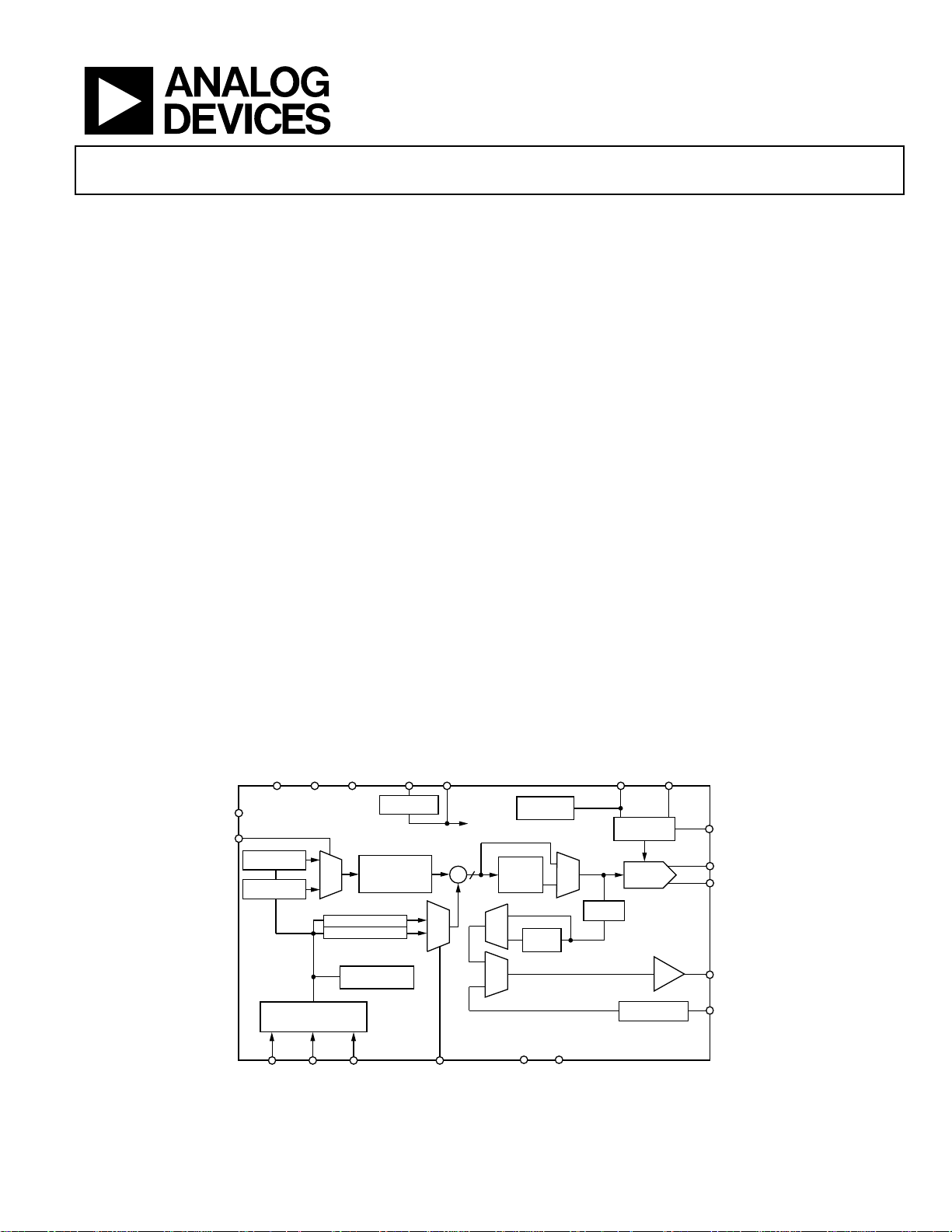
GENERAL DESCRIPTION
The AD9834 is a 75 MHz low power DDS device capable of
producing high performance sine and triangular outputs. It also
has an on-board comparator that allows a square wave to be
produced for clock generation. Consuming only 20 mW of power
at 3 V makes the AD9834 an ideal candidate for power-sensitive
applications.
FUNCTIONAL BLOCK DIAGRAM
DGND
CAP/2.5VDVDDAGNDAVDD
75 MHz Complete DDS
AD9834
Capability for phase modulation and frequency modulation is
provided. The frequency registers are 28 bits; with a 75 MHz clock
rate, resolution of 0.28 Hz can be achieved. Similarly, with a 1 MHz
clock rate, the AD9834 can be tuned to 0.004 Hz resolution.
Frequency and phase modulation are affected by loading registers
through the serial interface and toggling the registers using
software or the FSELECT pin and PSELECT pin, respectively.
The AD9834 is written to using a 3-wire serial interface. This
serial interface operates at clock rates up to 40 MHz and is
compatible with DSP and microcontroller standards.
The device operates with a power supply from 2.3 V to 5.5 V.
The analog and digital sections are independent and can be run
from different power supplies, for example, AVDD can equal
5 V with DVDD equal to 3 V.
The AD9834 has a power-down pin (SLEEP) that allows
external control of the power-down mode. Sections of the
device that are not being used can be powered down to
minimize the current consumption. For example, the DAC can
be powered down when a clock output is being generated.
The part is available in a 20-lead TSSOP.
REFOUT FS ADJUST
MCLK
FSELECT
28-BIT FREQ0
REG
28-BIT FREQ1
REG
SERIAL I NTERFACE
FSYNC SCLK SDATA
Rev. C
Information furnished by Analog Devices is believed to be accurate and reliable. However, no
responsibility is assumed by Anal og Devices for its use, nor for any infringements of patents or ot her
rights of third parties that may result from its use. Specifications subject to change without notice. No
license is granted by implication or otherwise under any patent or patent rights of Analog Devices.
Trademarks and registered trademarks are the property of their respective owners.
MUX
12-BIT PHASE 0 REG
12-BIT PHASE 1 REG
AND
CONTROL L OGIC
REGULATO R
PHASE
ACCUMULATOR
(28-BIT)
16-BIT CONT ROL
REGISTER
Σ
MUX
VCC
2.5V
12
MUX
MUX
Figure 1.
ON-BOARD
REFERENCE
SIN
ROM
SLEEP RESETPSELECT
MUX
DIVIDED
BY 2
One Technology Way, P.O. Box 9106, Norwood, MA 02062-9106, U.S.A.
Tel: 781.329.4700 www.analog.com
Fax: 781.461.3113 ©2003–2011 Analog Devices, Inc. All rights reserved.
MSB
FULL-SCALE
CONTROL
10-BIT
DAC
COMPARATOR
AD9834
COMP
IOUT
IOUTB
SIGN BIT OUT
VIN
02705-001
Page 2

AD9834
TABLE OF CONTENTS
Features.............................................................................................. 1
Control Register ......................................................................... 18
Applications....................................................................................... 1
General Description ......................................................................... 1
Functional Block Diagram .............................................................. 1
Revision History ............................................................................... 3
Specifications..................................................................................... 4
Timing Characteristics ................................................................ 6
Absolute Maximum Ratings............................................................ 7
ESD Caution.................................................................................. 7
Pin Configuration and Function Descriptions............................. 8
Typical Performance Characteristics ........................................... 10
Terminology ....................................................................................14
Theory of Operation ...................................................................... 15
Circuit Description......................................................................... 16
Numerically Controlled Oscillator Plus Phase Modulator... 16
SIN ROM..................................................................................... 16
Frequency and Phase Registers ................................................ 20
Writing to a Frequency Register............................................... 21
Writing to a Phase Register....................................................... 21
RESET Function......................................................................... 21
SLEEP Function.......................................................................... 21
SIGN BIT OUT Pin.................................................................... 22
The IOUT and IOUTB Pins...................................................... 22
Applications Information.............................................................. 23
Grounding and Layout .................................................................. 26
Interfacing to Microprocessors..................................................... 27
AD9834 to ADSP-21xx Interface ............................................. 27
AD9834 to 68HC11/68L11 Interface....................................... 27
AD9834 to 80C51/80L51 Interface.......................................... 28
AD9834 to DSP56002 Interface ............................................... 28
Evaluation Board............................................................................ 29
Digital-to-Analog Converter (DAC) ....................................... 16
Comparator................................................................................. 16
Regulator...................................................................................... 17
Output Voltage Compliance...................................................... 17
Functional Description.................................................................. 18
Serial Interface ............................................................................ 18
Powering Up the AD9834 ......................................................... 18
Latency......................................................................................... 18
System Development Platform................................................. 29
AD9834 to SPORT Interface..................................................... 29
XO vs. External Clock................................................................ 29
Power Supply............................................................................... 29
Evaluation Board Schematics ................................................... 30
Evaluation Board Layout........................................................... 32
Outline Dimensions....................................................................... 35
Ordering Guide .......................................................................... 35
Rev. C | Page 2 of 36
Page 3

AD9834
REVISION HISTORY
2/11—Rev. B to Rev. C
Changes to I
Changes to FS ADJUST Description, Table 4................................8
Added Output Voltage Compliance Section................................17
Changes to Figure 31 ......................................................................23
Changes to Figure 32 ......................................................................24
Deleted Using the AD9834 Evaluation Board Section and the
Prototyping Area Section...............................................................28
Added System Development Platform Section, AD9834 to
SPORT Interface Section, Figure 39, and Figure 40;
Renumbered Sequentially ..............................................................29
Changes to XO vs. External Clock Section and Power Supply
Section ..............................................................................................29
Deleted Bill of Materials, Table 19;
Renumbered Sequentially ..............................................................30
Added Evaluation Board Schematics Section and Figure 41 ....30
Added Figure 42 ..............................................................................31
Added Evaluation Board Layout Section and Figure 43............32
Added Figure 44 ..............................................................................33
Added Figure 45 ..............................................................................34
Changes to Ordering Guide...........................................................35
Parameter, Table 1 ..................................................5
DD
4/10—Rev. A to Rev. B
Changes to Comparator Section ...................................................15
Added Figure 28..............................................................................16
Changes to Serial Interface Section ..............................................17
8/06—Rev. 0 to Rev. A
Updated Format ................................................................. Universal
Changed to 75 MHz Complete DDS ............................... Universal
Changes to Features Section............................................................1
Changes to Table 1 ............................................................................4
Changes to Table 2 ............................................................................6
Changes to Table 3 ............................................................................8
Added Figure 10, Figures Renumbered Sequentially................... 9
Added Figure 16 and Figure 17, Figures Renumbered
Sequentially......................................................................................10
Changes to Table 6 ..........................................................................19
Changes to Writing a Frequency Register Section .....................20
Changes to Figure 29 ......................................................................21
Changes to Table 19 ........................................................................30
Changes to Figure 38 ......................................................................28
2/03—Revision 0: Initial Version
Rev. C | Page 3 of 36
Page 4

AD9834
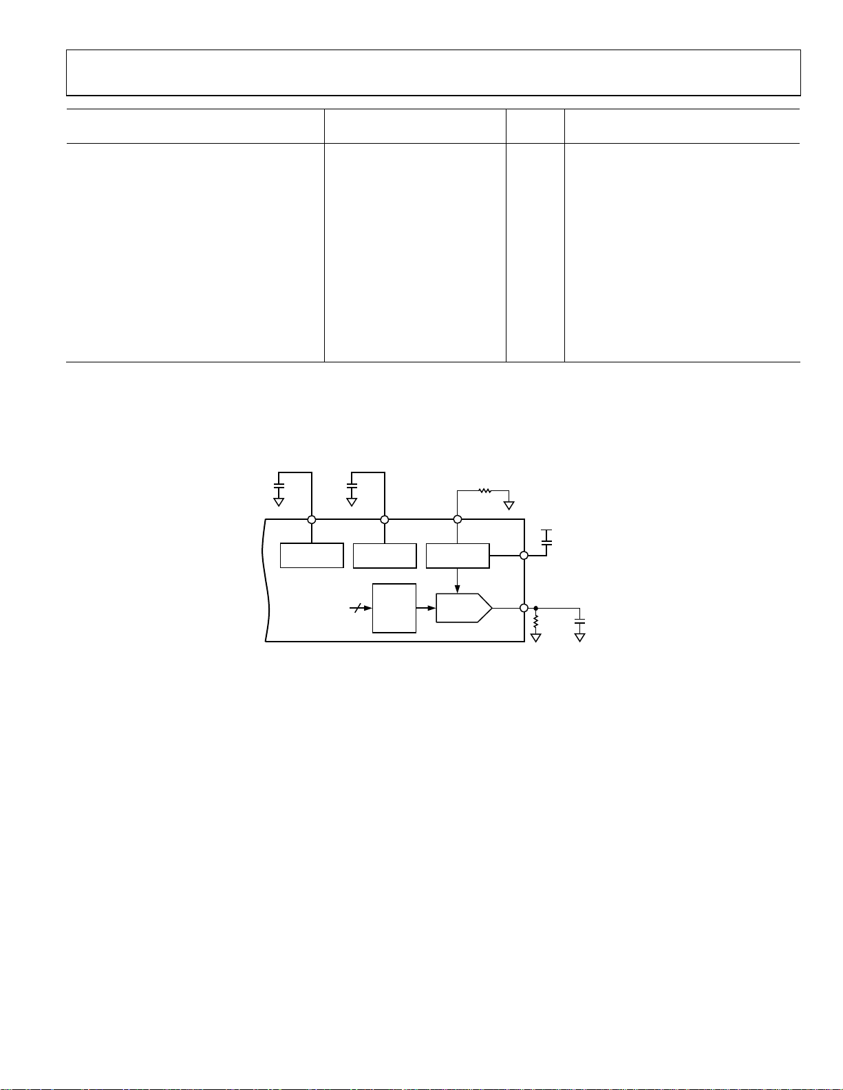
SPECIFICATIONS
VDD = 2.3 V to 5.5 V, AGND = DGND = 0 V, TA = T
Table 1.
Grade B, Grade C1
Parameter2 Min Typ Max Unit Test Conditions/Comments
SIGNAL DAC SPECIFICATIONS
Resolution 10 Bits
Update Rate 75 MSPS
I
Full Scale3 3.0 mA
OUT
V
Max 0.6 V
OUT
V
Min 30 mV
OUT
Output Compliance4 0.8 V
DC Accuracy
Integral Nonlinearity ±1 LSB
Differential Nonlinearity ±0.5 LSB
DDS SPECIFICATIONS
Dynamic Specifications
Signal-to-Noise Ratio 55 60 dB f
Total Harmonic Distortion −66 −56 dBc f
Spurious-Free Dynamic Range (SFDR)
Wideband (0 to Nyquist) −60 −56 dBc f
Narrow Band (±200 kHz)
B Grade −78 −67 dBc f
C Grade −74 −65 dBc f
Clock Feedthrough −50 dBc
Wake-Up Time 1 ms
COMPARATOR
Input Voltage Range 1 V p-p AC-coupled internally
Input Capacitance 10 pF
Input High-Pass Cutoff Frequency 4 MHz
Input DC Resistance 5 MΩ
Input Leakage Current 10 A
OUTPUT BUFFER
Output Rise/Fall Time 12 ns Using a 15 pF load
Output Jitter 120 ps rms 3 MHz sine wave, 0.6 V p-p
VOLTAGE REFERENCE
Internal Reference 1.12 1.18 1.24 V
REFOUT Output Impedance5 1 kΩ
Reference Temperature Coefficient 100 ppm/°C
LOGIC INPUTS
Input High Voltage, V
1.7 V 2.3 V to 2.7 V power supply
INH
2.0 V 2.7 V to 3.6 V power supply
2.8 V 4.5 V to 5.5 V power supply
Input Low Voltage, V
0.6 V 2.3 V to 2.7 V power supply
INL
0.7 V 2.7 V to 3.6 V power supply
0.8 V 4.5 V to 5.5 V power supply
Input Current, I
10 µA
INH/IINL
Input Capacitance, CIN 3 pF
MIN
to T
MAX
, R
SET
= 6.8 k, R
= 200 for IOUT and IOUTB, unless otherwise noted.
LOAD
= 75 MHz, f
MCLK
= 75 MHz, f
MCLK
= 75 MHz, f
MCLK
= 50 MHz, f
MCLK
= 75 MHz, f
MCLK
OUT
OUT
OUT
OUT
OUT
= f
= f
= f
= f
= f
MCLK
MCLK
MCLK
MCLK
MCLK
/4096
/4096
/75
/50
/75
Rev. C | Page 4 of 36
Page 5
AD9834
F
Grade B, Grade C1
Parameter2 Min Typ Max Unit Test Conditions/Comments
POWER SUPPLIES
AVDD 2.3 5.5 V f
DVDD 2.3 5.5 V
6
I
3.8 5 mA
AA
6
I
DD
B Grade 2.0 3 mA IDD code dependent (see Figure 8)
C Grade 2.7 3.7 mA IDD code dependent (see Figure 8)
6
IAA + I
DD
B Grade 5.8 8 mA
C Grade 6.5 8.7 mA
Low Power Sleep Mode
B Grade 0.5 mA DAC powered down, MCLK running
C Grade 0.6 mA DAC powered down, MCLK running
1
B grade: MCLK = 50 MHz; C grade: MCLK = 75 MHz. For specifications that do not specify a grade, the value applies to both grades.
2
Operating temperature range is as follows: B, C versions: −40°C to +105°C, typical specifications are at 25°C.
3
For compliance, with specified load of 200 Ω, I
4
Guaranteed by design.
5
Applies when REFOUT is sourcing current. The impedance is higher when REFOUT is sinking current.
6
Measured with the digital inputs static and equal to 0 V or DVDD.
100n
full scale should not exceed 4 mA.
OUT
10nF
R
SET
6.8kΩ
= 75 MHz, f
MCLK
OUT
= f
MCLK
/4096
ON-BOARD
REFERENCE
12
SIN
ROM
REFOUT
FULL-SCAL E
CONTROL
10-BIT DAC
CAP/2.5V
REGULATOR
AD9834
Figure 2. Test Circuit Used to Test the Specifications
FS ADJUST
COMP
IOUT
AVDD
R
LOAD
200Ω
10nF
20pF
02705-002
Rev. C | Page 5 of 36
Page 6
AD9834
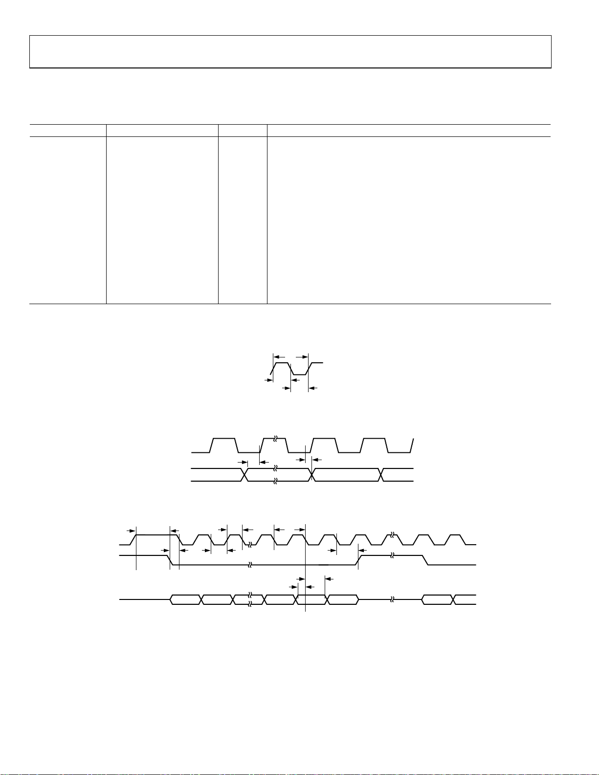
TIMING CHARACTERISTICS
DVDD = 2.3 V to 5.5 V, AGND = DGND = 0 V, unless otherwise noted.
Table 2.
Parameter1 Limit at T
t1 20/13.33 ns min MCLK period: 50 MHz/75 MHz
t2 8/6 ns min MCLK high duration: 50 MHz/75 MHz
t3 8/6 ns min MCLK low duration: 50 MHz/75 MHz
t4 25 ns min SCLK period
t5 10 ns min SCLK high duration
t6 10 ns min SCLK low duration
t7 5 ns min FSYNC-to-SCLK falling edge setup time
t
10 ns min FSYNC-to-SCLK hold time
8 MIN
t
t4 − 5 ns max
8 MAX
t9 5 ns min Data setup time
t10 3 ns min Data hold time
t11 8 ns min FSELECT, PSELECT setup time before MCLK rising edge
t
8 ns min FSELECT, PSELECT setup time after MCLK rising edge
11A
t12 5 ns min SCLK high to FSYNC falling edge setup time
1
Guaranteed by design, not production tested.
MIN
to T
Unit Test Conditions/Comments
MAX
Timing Diagrams
SCLK
FSYNC
SDATA
t
12
t
1
MCLK
t
2
t
3
02705-003
Figure 3. Master Clock
MCLK
t
11A
FSELECT,
PSELECT
t
11
VALID DATA VALID DATA VAL ID DATA
Figure 4. Control Timing
t
5
t
7
D15 D14 D2 D1 D15 D14
t
6
t
4
t
8
t
10
t
9
D0
Figure 5. Serial Timing
02705-004
02705-005
Rev. C | Page 6 of 36
Page 7
AD9834
ABSOLUTE MAXIMUM RATINGS
TA = 25°C, unless otherwise noted.
Table 3.
Parameter Ratings
AVDD to AGND −0.3 V to +6 V
DVDD to DGND −0.3 V to +6 V
AVDD to DVDD −0.3 V to +0.3 V
AGND to DGND −0.3 V to +0.3 V
CAP/2.5V 2.75 V
Digital I/O Voltage to DGND −0.3 V to DVDD + 0.3 V
Analog I/O Voltage to AGND −0.3 V to AVDD + 0.3 V
Operating Temperature Range
Industrial (B Version) −40°C to +105°C
Storage Temperature Range −65°C to +150°C
Maximum Junction Temperature 150°C
TSSOP Package
θJA Thermal Impedance 143°C/W
θJC Thermal Impedance 45°C/W
Lead Temperature, Soldering (10 sec) 300°C
IR Reflow, Peak Temperature 220°C
Reflow Soldering (Pb-Free)
Peak Temperature 260°C (+0/–5)
Time at Peak Temperature 10 sec to 40 sec
Stresses above those listed under Absolute Maximum Ratings
may cause permanent damage to the device. This is a stress
rating only; functional operation of the device at these or any
other conditions above those indicated in the operational
section of this specification is not implied. Exposure to absolute
maximum rating conditions for extended periods may affect
device reliability.
ESD CAUTION
Rev. C | Page 7 of 36
Page 8
AD9834
PIN CONFIGURATION AND FUNCTION DESCRIPTIONS
FS ADJUST
REFOUT
COMP
AVD D
DVDD
CAP/2.5V
DGND
MCLK
FSELECT
PSELECT
1
2
3
AD9834
4
TOP VIEW
(Not to Scale)
5
6
7
8
9
10
20
IOUTB
19
IOUT
18
AGND
17
VIN
16
SIGN BIT OUT
15
FSYNC
14
SCLK
13
SDATA
12
SLEEP
11
RESET
02705-006
Figure 6. Pin Configuration
Table 4. Pin Function Descriptions
Pin No. Mnemonic Description
ANALOG SIGNAL AND REFERENCE
1 FS ADJUST
Full-Scale Adjust Control. A resistor (R
of the full-scale DAC current. The relationship between R
IOUT
= 18 × FSADJUST/R
FULL SCALE
FSADJUST = 1.15 V nominal, R
) is connected between this pin and AGND. This determines the magnitude
SET
SET
= 6.8 kΩ typical.
SET
and the full-scale current is as follows:
SET
2 REFOUT Voltage Reference Output. The AD9834 has an internal 1.20 V reference that is made available at this pin.
3 COMP DAC Bias Pin. This pin is used for decoupling the DAC bias voltage.
17 VIN
Input to Comparator. The comparator can be used to generate a square wave from the sinusoidal DAC output. The
DAC output should be filtered appropriately before being applied to the comparator to improve jitter. When Bit
OPBITEN and Bit SIGN/PIB in the control register are set to 1, the comparator input is connected to VIN.
19, 20
IOUT,
IOUTB
Current Output. This is a high impedance current source. A load resistor of nominally 200 Ω should be connected
between IOUT and AGND. IOUTB should preferably be tied through an external load resistor of 200 Ω to AGND, but
it can be tied directly to AGND. A 20 pF capacitor to AGND is also recommended to prevent clock feedthrough.
POWER SUPPLY
4 AVDD
Positive Power Supply for the Analog Section. AVDD can have a value from 2.3 V to 5.5 V. A 0.1 F decoupling
capacitor should be connected between AVDD and AGND.
5 DVDD
Positive Power Supply for the Digital Section. DVDD can have a value from 2.3 V to 5.5 V. A 0.1 F decoupling
capacitor should be connected between DVDD and DGND.
6 CAP/2.5V
The digital circuitry operates from a 2.5 V power supply. This 2.5 V is generated from DVDD using an on-board
regulator (when DVDD exceeds 2.7 V). The regulator requires a decoupling capacitor of typically 100 nF that is
connected from CAP/2.5 V to DGND. If DVDD is equal to or less than 2.7 V, CAP/2.5 V should be shorted to DVDD.
7 DGND Digital Ground.
18 AGND Analog Ground.
DIGITAL INTERFACE AND CONTROL
8 MCLK
Digital Clock Input. DDS output frequencies are expressed as a binary fraction of the frequency of MCLK. The
output frequency accuracy and phase noise are determined by this clock.
9 FSELECT
Frequency Select Input. FSELECT controls which frequency register, FREQ0 or FREQ1, is used in the phase
accumulator. The frequency register to be used can be selected using Pin FSELECT or Bit FSEL. When Bit FSEL is
used to select the frequency register, the FSELECT pin should be tied to CMOS high or low.
10 PSELECT
Phase Select Input. PSELECT controls which phase register, PHASE0 or PHASE1, is added to the phase accumulator
output. The phase register to be used can be selected using Pin PSELECT or Bit PSEL. When the phase registers are being
controlled by Bit PSEL, the PSELECT pin should be tied to CMOS high or low.
11 RESET
Active High Digital Input. RESET resets appropriate internal registers to zero; this corresponds to an analog output
of midscale. RESET does not affect any of the addressable registers.
12 SLEEP
Active High Digital Input. When this pin is high, the DAC is powered down. This pin has the same function as
Control Bit SLEEP12.
Rev. C | Page 8 of 36
Page 9

AD9834
Pin No. Mnemonic Description
13 SDATA Serial Data Input. The 16-bit serial data-word is applied to this input.
14 SCLK Serial Clock Input. Data is clocked into the AD9834 on each falling SCLK edge.
15 FSYNC
16
SIGN BIT
OUT
Active Low Control Input. This is the frame synchronization signal for the input data. When FSYNC is taken low, the
internal logic is informed that a new word is being loaded into the device.
Logic Output. The comparator output is available on this pin or, alternatively, the MSB from the NCO can be output
on this pin. Setting Bit OPBITEN in the control register to 1 enables this output pin. Bit SIGN/PIB determines
whether the comparator output or the MSB from the NCO is output on the pin.
Rev. C | Page 9 of 36
Page 10
AD9834
–
–
TYPICAL PERFORMANCE CHARACTERISTICS
4.0
T
= 25°C
A
3.5
0
AVDD = DVDD = 3V
T
= 25°C
A
–10
3.0
2.5
2.0
(mA)
DD
I
1.5
1.0
0.5
0
0
15 30 45 60
MCLK FREQUENCY (MHz)
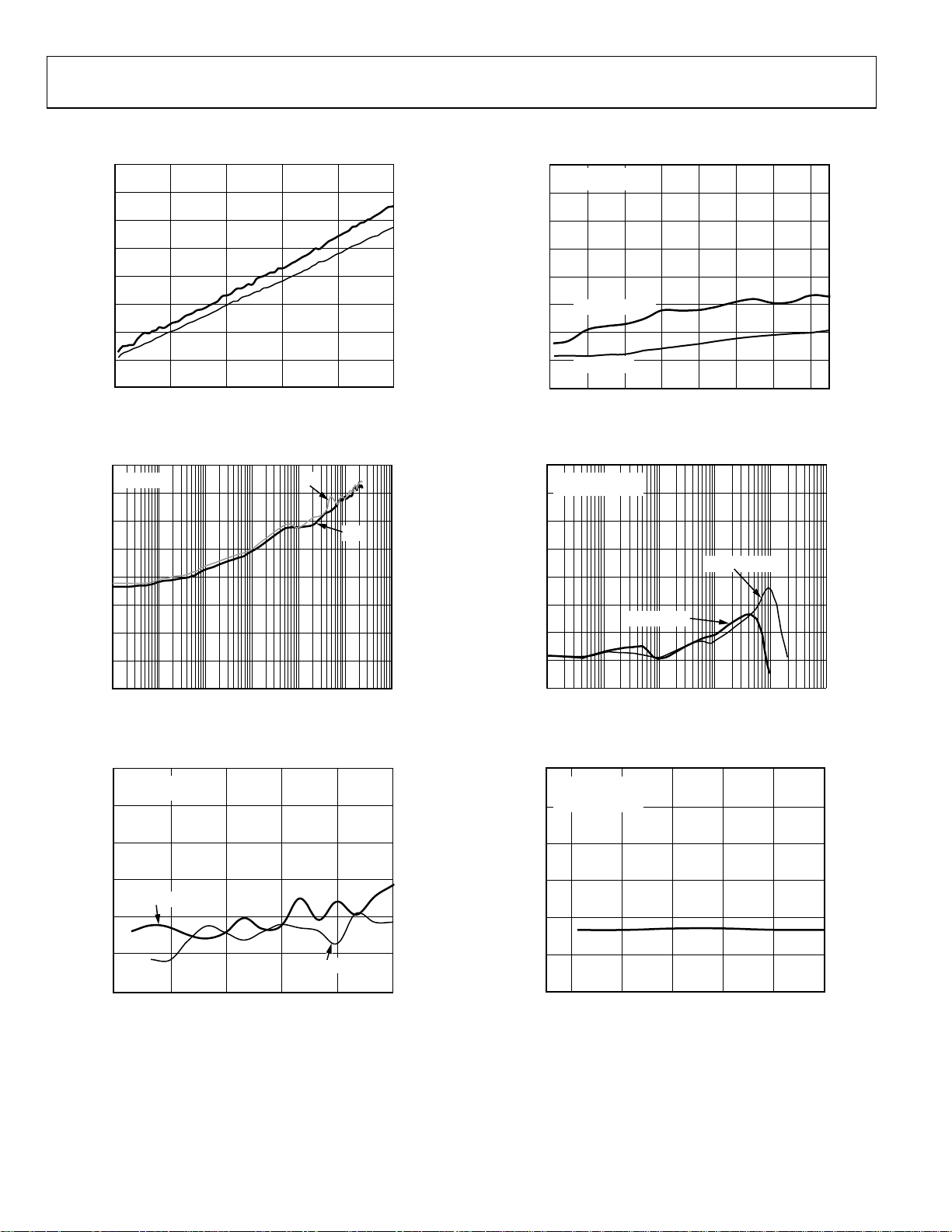
Figure 7. Typical Current Consumption (I
4.0
TA = 25°C
3.5
3.0
2.5
2.0
(mA)
DD
I
1.5
1.0
0.5
5V
3V
) vs. MCLK Frequency
DD
5V
–20
–30
–40
SFDR (dBc)
–50
–60
–70
75
02705-007
–80
SFDR dB MCLK/7
f
= 1MHz
OUT
0 10203040506070
MCLK FREQUENCY (MHz)
02705-010
Figure 10. Wideband SFDR vs. MCLK Frequency
0
AVDD = DVDD = 3V
T
= 25°C
A
–10
3V
–20
–30
–40
SFDR (dBc)
–50
–60
–70
30MHz CLOCK
50MHz CLOCK
0
100 1k 10k 100k 1M 10M 100M
Figure 8. Typical I
60
AVDD = DVDD = 3V
T
= 25°C
A
–65
–70
–75
SFDR dB MCLK/ 50
SFDR (dBc)
–80
–85
–90
01530456075
f
(Hz)
OUT
vs. f
for f
DD
OUT
MCLK
SFDR dB MCLK/7
MCLK FREQUENCY ( MHz)
= 50 MHz
Figure 9. Narrow-Band SFDR vs. MCLK Frequency
–80
0.001 0.01 0.1 1. 0 10 100
02705-008
Figure 11. Wideband SFDR vs. f
40
TA = 25°C
AVDD = DVDD = 3V
= MCLK/4096
f
OUT
–45
–50
–55
SNR (dB)
–60
–65
–70
1.0 5.0 10. 0 12.5 25.0 50.0
02705-009
f
OUT/fMCLK
for Various MCLK Frequencies
OUT/fMCLK
MCLK FREQUENCY ( MHz)
2705-011
02705-012
Figure 12. SNR vs. MCLK Frequency
Rev. C | Page 10 of 36
Page 11
AD9834
–
1000
950
900
850
800
750
700
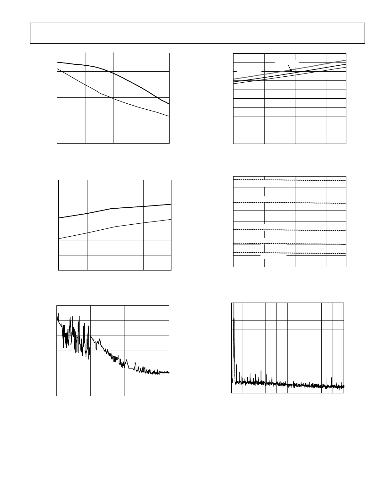
WAKE-UP TIME (µs)
650
600
550
500
–40 25 105
5.5V
TEMPERATURE (° C)
2.3V
Figure 13. Wake-Up Time vs. Temperature
02705-013
0.20
0.18
0.16
DVDD = 2.3V
0.14
0.12
0.10
DVDD (V)
0.08
0.06
0.04
0.02
0
–40–200 20406080100
Figure 16. SIGN BIT OUT Low Level, I
DVDD = 3.3V
TEMPERATURE (°C)
DVDD = 5.5V
= 1 mA
SINK
02705-037
1.250
1.225
UPPER RANGE
1.200
(V)
1.175
(REFOUT)
V
1.150
1.125
1.100
–40 25 105
Figure 14. V
100
–110
–120
–130
(dBc/Hz)
–140
–150
–160
100 1k 10k 100k 200k
Figure 15. Output Phase Noise, f
LOWER RANGE
TEMPERATURE ( °C)
vs. Temperature
REFOUT
FREQUENCY (Hz)
= 2 MHz, MCLK = 50 MHz
OUT
AVDD = DVDD = 5V
T
= 25°C
A
5.5
5.0
4.5
4.0
3.5
DVDD (V)
3.0
2.5
2.0
1.5
–40–200 20406080100
2705-014
Figure 17. SIGN BIT OUT High Level, I
0
–10
–20
–30
–40
–50
(dB)
–60
–70
–80
–90
–100
0 100k
RWB 100 ST 100 SECVWB 30
02705-015
Figure 18. f
MCLK
DVDD = 5.5V
DVDD = 4.5V
DVDD = 3.3V
DVDD = 2.7V
DVDD = 2.3V
= 10 MHz; f
TEMPERATURE (°C)
= 1 mA
SINK
FREQUENCY (Hz)
= 2.4 kHz, Frequency Word = 000FBA9
OUT
02705-038
02705-016
Rev. C | Page 11 of 36
Page 12

AD9834
0
–10
–20
–30
–40
–50
(dB)
–60
–70
–80
–90
–100
0
RWB 1k ST 50 SECVWB 300
0
–10
–20
–30
–40
–50
(dB)
–60
–70
–80
–90
–100
05M
RWB 1k ST 50 SECVWB 300
0
–10
–20
–30
–40
–50
(dB)
–60
–70
–80
–90
–100
0 160k
RWB 100 ST 200 SEC
Figure 21. f
Figure 19. f
Figure 20. f
= 50 MHz; f
MCLK
FREQUENCY (Hz)
= 10 MHz; f
MCLK
= 1.43 MHz = f
OUT
Frequency Word = 2492492
FREQUENCY (Hz)
= 10 MHz; f
MCLK
= 3.33 MHz = f
OUT
Frequency Word = 5555555
VWB 30
FREQUENCY (Hz)
= 12 kHz, Frequency Word = 000FBA9
OUT
MCLK
MCLK
/7,
/3,
5M
0
–10
–20
–30
–40
–50
(dB)
–60
–70
–80
–90
–100
01
RWB 100 ST 200 SECVWB 300
02705-017
Figure 22. f
= 50 MHz; f
MCLK
FREQUENCY (Hz)
= 120 kHz, Frequency Word = 009D496
OUT
.6M
2705-020
0
–10
–20
–30
–40
–50
(dB)
–60
–70
–80
–90
–100
02
2705-018
02705-019
RWB 1k ST 200 SECVWB 300
Figure 23. f
–10
–20
–30
–40
–50
(dB)
–60
–70
–80
–90
–100
Figure 24. f
= 50 MHz; f
MCLK
0
0 25M
RWB 1k ST 200 SECVWB 300
= 50 MHz; f
MCLK
FREQUENCY (Hz)
= 1.2 MHz, Frequency Word = 0624DD3
OUT
FREQUENCY (Hz)
= 4.8 MHz, Frequency Word = 189374C
OUT
5M
02705-021
02705-022
Rev. C | Page 12 of 36
Page 13

AD9834
0
–10
–20
–30
–40
–50
(dB)
–60
–70
–80
–90
–100
0 25M
RWB 1k ST 200 SECVWB 300
Figure 25. f
= 50 MHz; f
MCLK
FREQUENCY (Hz)
= 7.143 MHz = f
OUT
MCLK
/7,
02705-023
Frequency Word = 2492492
0
–10
–20
–30
–40
–50
(dB)
–60
–70
–80
–90
–100
0 25M
RWB 1k ST 200 SE CVWB 300
Figure 26. f
= 50 MHz; f
MCLK
FREQUENCY (Hz)
= 16.667 MHz = f
OUT
Frequency Word = 5555555
MCLK
/3,
02705-024
Rev. C | Page 13 of 36
Page 14

AD9834
TERMINOLOGY
Integral Nonlinearity (INL)
INL is the maximum deviation of any code from a straight line
passing through the endpoints of the transfer function. The
endpoints of the transfer function are zero scale, a point 0.5 LSB
below the first code transition (000 . . . 00 to 000 . . . 01), and full
scale, a point 0.5 LSB above the last code transition (111 . . . 10 to
111 . . . 11). The error is expressed in LSBs.
Differential Nonlinearity (DNL)
DNL is the difference between the measured and ideal 1 LSB
change between two adjacent codes in the DAC. A specified
DNL of ±1 LSB maximum ensures monotonicity.
Output Compliance
The output compliance refers to the maximum voltage that can
be generated at the output of the DAC to meet the specifications.
When voltages greater than that specified for the output compliance are generated, the AD9834 may not meet the
specifications listed in the data sheet.
spur relative to the magnitude of the fundamental frequency in
the 0 to Nyquist bandwidth. The narrow-band SFDR gives the
attenuation of the largest spur or harmonic in a bandwidth of
±200 kHz about the fundamental frequency.
Total Harmonic Distortion (THD)
THD is the ratio of the rms sum of harmonics to the rms value
of the fundamental. For the AD9834, THD is defined as
22222
VVVVV
++++
THD
V
where
V
, V5, and V6 are the rms amplitudes of the second harmonic
4
log20
=
is the rms amplitude of the fundamental and V2, V3,
1
V
1
65432
through the sixth harmonic.
Signal-to-Noise Ratio (SNR)
SNR is the ratio of the rms value of the measured output signal
to the rms sum of all other spectral components below the
Nyquist frequency. The value for SNR is expressed in decibels.
Spurious-Free Dynamic Range (SFDR)
Along with the frequency of interest, harmonics of the
fundamental frequency and images of these frequencies are
present at the output of a DDS device. The SFDR refers to the
largest spur or harmonic present in the band of interest. The
wideband SFDR gives the magnitude of the largest harmonic or
Clock Feedthrough
There is feedthrough from the MCLK input to the analog
output. Clock feedthrough refers to the magnitude of the
MCLK signal relative to the fundamental frequency in the
output spectrum of the AD9834.
Rev. C | Page 14 of 36
Page 15

AD9834
2p
THEORY OF OPERATION
Sine waves are typically thought of in terms of their magnitude
form a(t) = sin (ωt). However, these are nonlinear and not easy
to generate except through piecewise construction. On the
other hand, the angular information is linear in nature, that is,
the phase angle rotates through a fixed angle for each unit of
time. The angular rate depends on the frequency of the signal
MAGNITUDE
2π
2π
PHASE
f.
4π
4π
6π
6π
02705-025
by the traditional rate of ω = 2π
+1
0
–1
0
Figure 27. Sine Wave
Knowing that the phase of a sine wave is linear and given a
reference interval (clock period), the phase rotation for that
period can be determined.
Phase = ω∆t
∆
Solving for ω,
ω = ∆Phase/∆t = 2πf
Solving for f and substituting the reference clock frequency for
the reference period (1/
f = ∆Phase × f
MCLK
f
MCLK
/2π
= ∆t),
The AD9834 builds the output based on this simple equation. A
simple DDS chip can implement this equation with three major
subcircuits: numerically controlled oscillator + phase modulator,
SIN ROM, and digital-to-analog converter (DAC). Each of these
subcircuits is discussed in the Circuit Description section.
Rev. C | Page 15 of 36
Page 16

AD9834
CIRCUIT DESCRIPTION
The AD9834 is a fully integrated direct digital synthesis (DDS)
chip. The chip requires one reference clock, one low precision
resistor, and eight decoupling capacitors to provide digitally created
sine waves up to 37.5 MHz. In addition to the generation of this RF
signal, the chip is fully capable of a broad range of simple and
complex modulation schemes. These modulation schemes are
fully implemented in the digital domain, allowing accurate and
simple realization of complex modulation algorithms using DSP
techniques.
The internal circuitry of the AD9834 consists of the following
main sections: a numerically controlled oscillator (NCO),
frequency and phase modulators, SIN ROM, a DAC, a
comparator, and a regulator.
NUMERICALLY CONTROLLED OSCILLATOR PLUS PHASE MODULATOR
This consists of two frequency select registers, a phase accumulator,
two phase offset registers, and a phase offset adder. The main
component of the NCO is a 28-bit phase accumulator. Continuous
time signals have a phase range of 0 π to 2π. Outside this range of
numbers, the sinusoid functions repeat themselves in a periodic
manner. The digital implementation is no different. The
accumulator simply scales the range of phase numbers into a
multibit digital word. The phase accumulator in the AD9834 is
implemented with 28 bits. Therefore, in the AD9834, 2π = 2
Likewise, the ∆Phase term is scaled into this range of numbers:
0 < ∆
Phase < 2
28
− 1.
Making these substitutions into the previous equation
f = ∆Phase × f
where 0 < ∆
Phase < 2
MCLK
/228
28
− 1.
The input to the phase accumulator can be selected either from
the FREQ0 register or FREQ1 register and is controlled by the
FSELECT pin or the FSEL bit. NCOs inherently generate continuous phase signals, thus avoiding any output discontinuity
when switching between frequencies.
Following the NCO, a phase offset can be added to perform
phase modulation using the 12-bit phase registers. The contents
of one of these phase registers is added to the MSBs of the NCO.
The AD9834 has two phase registers, the resolution of these
registers being 2π/4096.
28
.
SIN ROM
To make the output from the NCO useful, it must be converted
from phase information into a sinusoidal value. Phase information maps directly into amplitude; therefore, the SIN ROM uses
the digital phase information as an address to a look-up table
and converts the phase information into amplitude.
Although the NCO contains a 28-bit phase accumulator, the
output of the NCO is truncated to 12 bits. Using the full resolution of the phase accumulator is impractical and unnecessary
28
because it requires a look-up table of 2
entries. It is necessary
only to have sufficient phase resolution such that the errors due
to truncation are smaller than the resolution of the 10-bit DAC.
This requires the SIN ROM to have two bits of phase resolution
more than the 10-bit DAC.
The SIN ROM is enabled using the OPBITEN and MODE bits
in the control register. This is explained further in Ta b le 1 8.
DIGITAL-TO-ANALOG CONVERTER (DAC)
The AD9834 includes a high impedance current source 10-bit
DAC capable of driving a wide range of loads. The full-scale
output current can be adjusted for optimum power and external
load requirements using a single external resistor (R
SET
).
The DAC can be configured for either single-ended or differential
operation. IOUT and IOUTB can be connected through equal
external resistors to AGND to develop complementary output
voltages. The load resistors can be any value required, as long as
the full-scale voltage developed across it does not exceed the
voltage compliance range. Because full-scale current is
controlled by R
, adjustments to R
SET
can balance changes
SET
made to the load resistors.
COMPARATOR
The AD9834 can be used to generate synthesized digital clock
signals. This is accomplished by using the on-board self-biasing
comparator that converts the sinusoidal signal of the DAC to a
square wave. The output from the DAC can be filtered externally
before being applied to the comparator input. The comparator
reference voltage is the time average of the signal applied to V
The comparator can accept signals in the range of approximately
100 mV p-p to 1 V p-p. As the comparator input is ac-coupled, to
operate correctly as a zero crossing detector, it requires a minimum
input frequency of typically 3 MHz. The comparator output is a
square wave with an amplitude from 0 V to DVDD.
IN
.
Rev. C | Page 16 of 36
Page 17

AD9834
The AD9834 is a sampled signal with its output following
Nyquist sampling theorem. Specifically, its output spectrum
contains the fundamental plus aliased signals (images) that
occur at multiples of the reference clock frequency and the
selected output frequency. A graphical representation of the
sampled spectrum, with aliased images, is shown in Figure 28.
The prominence of the aliased images is dependent on the ratio
to MCLK. If ratio is small, the aliased images are very
of f
OUT
prominent and of a relatively high energy level as determined
by the sin(x)/x roll-off of the quantized DAC output. In fact,
depending on the f
/reference clock relationship, the first
OUT
aliased image can be on the order of −3 dB below the
fundamental.
A low-pass filter is generally placed between the output of the
DAC and the input of the comparator to further suppress the
effects of aliased images. Obviously, consideration must be
given to the relationship of the selected output frequency and
the reference clock frequency to avoid unwanted (and unexpected)
output anomalies. To apply the AD9834 as a clock generator,
limit the selected output frequency to <33% of reference clock
frequency, and thereby avoid generating aliased signals that fall
within, or close to, the output band of interest (generally dcselected output frequency). This practice eases the complexity
(and cost) of the external filter requirement for the clock
generator application. Refer to the AN-837 Application Note
for more information.
REGULATOR
The AD9834 has separate power supplies for the analog and
digital sections. AVDD provides the power supply required for
the analog section, and DVDD provides the power supply for
the digital section. Both of these supplies can have a value of
2.3 V to 5.5 V and are independent of each other. For example,
the analog section can be operated at 5 V, and the digital section
can be operated at 3 V, or vice versa.
The internal digital section of the AD9834 is operated at 2.5 V.
An on-board regulator steps down the voltage applied at DVDD
to 2.5 V. The digital interface (serial port) of the AD9834 also
operates from DVDD. These digital signals are level shifted
within the AD9834 to make them 2.5 V compatible.
When the applied voltage at the DVDD pin of the AD9834 is
equal to or less than 2.7 V, Pin CAP/2.5V and Pin DVDD should
be tied together, thus bypassing the on-board regulator.
OUTPUT VOLTAGE COMPLIANCE
The AD9834 has a maximum current density, set by the R
of 4 mA. The maximum output voltage from the AD9834 is
− 1.5 V. This is to ensure that the output impedance of
V
DD
the internal switch does not change, affecting the spectral
performance of the part. For a minimum supply of 2.3 V, the
maximum output voltage is 0.8 V. Specifications in Tab l e 1 are
guaranteed with an R
of 6.8 kΩ and an R
SET
of 200 Ω.
LOAD
SET
,
To enable the comparator, Bit SIGN/PIB and Bit OPBITEN in
the control resister are set to 1. This is explained further in
Tabl e 1 7 .
f
OUT
SIGNAL AMPLITUDE
0Hz FIRST
sin x/x ENVELOPE
f/f
)
x = π (
C
f
–
f
C
OUT
f
C
IMAGE
SYSTEM CLOCK
f
+
f
C
OUT
SECOND
IMAGE
Figure 28. The DAC Output Spectrum
2
f
–
f
C
OUT
2
THIRD
IMAGE
FREQUENCY (Hz)
f
C
2
f
+
C
FOURTH
IMAGE
f
OUT
3
f
C
FIFTH
IMAGE
–
f
OUT
3
f
+
f
C
3
OUT
f
C
SIXTH
IMAGE
02705-040
Rev. C | Page 17 of 36
Page 18

AD9834
FUNCTIONAL DESCRIPTION
SERIAL INTERFACE
The AD9834 has a standard 3-wire serial interface that is compatible with SPI, QSPI™, MICROWIRE™, and DSP interface
standards.
Data is loaded into the device as a 16-bit word under the
control of a serial clock input (SCLK). The timing diagram
for this operation is given in Figure 5.
For a detailed example of programming the AD9833 and
AD9834 devices, refer to the AN-1070 Application Note.
to 0 to begin generating an output. The data appears on the
DAC output eight MCLK cycles after RESET is set to 0.
LATENCY
Latency is associated with each operation. When Pin FSELECT
and Pin PSELECT change value, there is a pipeline delay before
control is transferred to the selected register. When the t
timing specifications are met (see Figure 4), FSELECT and
t
11A
PSELECT have latencies of eight MCLK cycles. When the t
timing specifications are not met, the latency is increased by
t
11A
one MCLK cycle.
11
and
11
and
The FSYNC input is a level triggered input that acts as a frame
synchronization and chip enable. Data can only be transferred
into the device when FSYNC is low. To start the serial data
transfer, FSYNC should be taken low, observing the minimum
FSYNC-to-SCLK falling edge setup time (t
). After FSYNC goes
7
low, serial data is shifted into the input shift register of the
device on the falling edges of SCLK for 16 clock pulses. FSYNC
can be taken high after the 16th falling edge of SCLK, observing
the minimum SCLK falling edge to FSYNC rising edge time
). Alternatively, FSYNC can be kept low for a multiple of
(t
8
16 SCLK pulses and then brought high at the end of the data
transfer. In this way, a continuous stream of 16-bit words can be
loaded while FSYNC is held low, with FSYNC only going high
after the 16th SCLK falling edge of the last word is loaded.
The SCLK can be continuous, or alternatively, the SCLK can
idle high or low between write operations but must be high
when FSYNC goes low (t
).
12
POWERING UP THE AD9834
The flow chart in Figure 31 shows the operating routine for the
AD9834. When the AD9834 is powered up, the part should be
reset. This resets appropriate internal registers to 0 to provide
an analog output of midscale. To avoid spurious DAC outputs
during AD9834 initialization, the RESET bit/pin should be set
to 1 until the part is ready to begin generating an output. RESET
does not reset the phase, frequency, or control registers. These
registers contain invalid data, and, therefore, should be set to a
known value by the user. The RESET bit/pin should then be set
Similarly, there is a latency associated with each asynchronous
write operation. If a selected frequency/phase register is loaded
with a new word, there is a delay of eight to nine MCLK cycles
before the analog output changes. There is an uncertainty of one
MCLK cycle because it depends on the position of the MCLK
rising edge when the data is loaded into the destination register.
The negative transition of the RESET and SLEEP functions are
sampled on the internal falling edge of MCLK. Therefore, they
also have a latency associated with them.
CONTROL REGISTER
The AD9834 contains a 16-bit control register that sets up the
AD9834 as the user wants to operate it. All control bits, except
MODE, are sampled on the internal negative edge of MCLK.
Tabl e 6 describes the individual bits of the control register. The
different functions and the various output options from the
AD9834 are described in more detail in the Frequency and
Phase Registers section.
To inform the AD9834 that the contents of the control register
are to be altered, DB15 and DB14 must be set to 0 as shown in
Tabl e 5 .
Table 5. Control Register
DB15 DB14 DB13 . . . DB0
0 0 CONTROL bits
Rev. C | Page 18 of 36
Page 19

AD9834
SLEEP12
SLEEP1
ACCUMULATOR
MODE + OPBI TEN
SIGN/PIB
OPBITEN
PHASE
(28-BIT)
SIN
ROM
MUX
0
MUX
1
DIVIDE
0
BY 2
1
MSB
(LOW POWER)
COMPARATOR
1
MUX
0
10-BIT DAC
DIGITAL
OUTPUT
(ENABLE)
IOUT
IOUTB
VIN
SIGN BIT OUT
02705-026
Figure 29. Function of Control Bits
DB15 DB14 DB13 DB12 DB11 DB10 DB9 DB8 DB7 DB6 DB5 DB4 DB3 DB2 DB1 DB0
0 0 B28 HLB FSEL PSEL PIN/SW RESET SLEEP1 SLEEP12 OPBITEN SIGN/PIB DIV2 0 MODE 0
Table 6. Description of Bits in the Control Register
Bit Name Description
DB13 B28 Two write operations are required to load a complete word into either of the frequency registers.
B28 = 1 allows a complete word to be loaded into a frequency register in two consecutive writes. The first write
contains the 14 LSBs of the frequency word and the next write contains the 14 MSBs. The first two bits of each 16-bit
word define the frequency register the word is loaded to and should, therefore, be the same for both of the
consecutive writes. Refer to Table 10 for the appropriate addresses. The write to the frequency register occurs after both
words have been loaded. An example of a complete 28-bit write is shown in Table 11 . Note however, that consecutive
28-bit writes to the same frequency register are not allowed, switch between frequency registers to do this type of
function.
B28 = 0, the 28-bit frequency register operates as two 14-bit registers, one containing the 14 MSBs and the other
containing the 14 LSBs. This means that the 14 MSBs of the frequency word can be altered independent of the 14 LSBs,
and vice versa. To alter the 14 MSBs or the 14 LSBs, a single write is made to the appropriate frequency address. The
Control Bit DB12 (HLB) informs the AD9834 whether the bits to be altered are the 14 MSBs or 14 LSBs.
DB12 HLB
This control bit allows the user to continuously load the MSBs or LSBs of a frequency register ignoring the remaining
14 bits. This is useful if the complete 28-bit resolution is not required. HLB is used in conjunction with DB13 (B28). This
control bit indicates whether the 14 bits being loaded are being transferred to the 14 MSBs or 14 LSBs of the addressed
frequency register. DB13 (B28) must be set to 0 to be able to change the MSBs and LSBs of a frequency word separately.
When DB13 (B28) = 1, this control bit is ignored.
HLB = 1 allows a write to the 14 MSBs of the addressed frequency register.
HLB = 0 allows a write to the 14 LSBs of the addressed frequency register.
DB11 FSEL
The FSEL bit defines whether the FREQ0 register or the FREQ1 register is used in the phase accumulator. See Table 8 to
select a frequency register.
DB10 PSEL
The PSEL bit defines whether the PHASE0 register data or the PHASE1 register data is added to the output of the phase
accumulator. See Tabl e 9 to select a phase register.
DB9 PIN/SW
Functions that select frequency and phase registers, reset internal registers, and power down the DAC can be
implemented using either software or hardware. PIN/SW selects the source of control for these functions.
PIN/SW = 1 implies that the functions are being controlled using the appropriate control pins.
PIN/SW = 0 implies that the functions are being controlled using the appropriate control bits.
DB8 RESET RESET = 1 resets internal registers to 0, this corresponds to an analog output of midscale.
RESET = 0 disables RESET. This function is explained in the RESET Function section.
DB7 SLEEP1
SLEEP1 = 1, the internal MCLK is disabled. The DAC output remains at its present value as the NCO is no longer
accumulating.
SLEEP1 = 0, MCLK is enabled. This function is explained in the SLEEP Function section.
DB6 SLEEP12 SLEEP12 = 1 powers down the on-chip DAC. This is useful when the AD9834 is used to output the MSB of the DAC data.
SLEEP12 = 0 implies that the DAC is active. This function is explained in the SLEEP Function section.
Rev. C | Page 19 of 36
Page 20

AD9834
Bit Name Description
DB5 OPBITEN
OPBITEN = 1 enables the SIGN BIT OUT pin.
DB4 SIGN/PIB The function of this bit is to control what is output at the SIGN BIT OUT pin.
DB3 DIV2 DIV2 is used in association with SIGN/PIB and OPBITEN. Refer to Table 1 7 .
DIV2 = 1, the digital output is passed directly to the SIGN BIT OUT pin.
DIV2 = 0, the digital output/2 is passed directly to the SIGN BIT OUT pin.
DB2 Reserved This bit must always be set to 0.
DB1 MODE
MODE = 1, the SIN ROM is bypassed, resulting in a triangle output from the DAC.
DB0 Reserved This bit must always be set to 0.
The function of this bit is to control whether there is an output at the SIGN BIT OUT pin. This bit should remain at 0 if the
user is not using the SIGN BIT OUT pin.
OPBITEN = 0, the SIGN BIT OUT output buffer is put into a high impedance state, therefore no output is available at the
SIGN BIT OUT pin.
SIGN/PIB = 1, the on-board comparator is connected to SIGN BIT OUT. After filtering the sinusoidal output from the
DAC, the waveform can be applied to the comparator to generate a square waveform. Refer to Table 17 .
SIGN/PIB = 0, the MSB (or MSB/2) of the DAC data is connected to the SIGN BIT OUT pin. Bit DIV2 controls whether it is
the MSB or MSB/2 that is output.
The function of this bit is to control what is output at the IOUT pin/IOUTB pin. This bit should be set to 0 if the Control
Bit OPBITEN = 1.
MODE = 0, the SIN ROM is used to convert the phase information into amplitude information, resulting in a sinusoidal
signal at the output. See Table 18.
FREQUENCY AND PHASE REGISTERS
The AD9834 contains two frequency registers and two phase
registers. These are described in Tab l e 7 .
Table 7. Frequency/Phase Registers
Register Size Description
FREQ0 28 bits
FREQ1 28 bits
PHASE0 12 bits
PHASE1 12 bits
The analog output from the AD9834 is
f
/228 × FREQREG
MCLK
where
FREQREG is the value loaded into the selected frequency
register. This signal is phase shifted by
2π/4096 ×
where
PHASEREG is the value contained in the selected phase
register. Consideration must be given to the relationship of the
selected output frequency and the reference clock frequency to
avoid unwanted output anomalies.
Frequency Register 0. When either the
FSEL bit or FSELECT pin = 0, this register
defines the output frequency as a fraction
of the MCLK frequency.
Frequency Register 1. When either the
FSEL bit or FSELECT pin = 1, this register
defines the output frequency as a fraction
of the MCLK frequency.
Phase Offset Register 0. When either the
PSEL bit or PSELECT pin = 0, the contents
of this register are added to the output of
the phase accumulator.
Phase Offset Register 1. When either the
PSEL bit or PSELECT pin = 1, the contents
of this register are added to the output of
the phase accumulator.
PHASEREG
Rev. C | Page 20 of 36
Access to the frequency and phase registers is controlled by
both the FSELECT and PSELECT pins, and the FSEL and PSEL
control bits. If the Control Bit PIN/SW = 1, the pins control the
function; whereas, if PIN/SW = 0, the bits control the function.
This is outlined in Tabl e 8 and Ta b le 9 . If the FSEL and PSEL
bits are used, the pins should be held at CMOS logic high or
low. Control of the frequency/phase registers is interchangeable
from the pins to the bits.
Table 8. Selecting a Frequency Register
FSELECT FSEL PIN/SW Selected Register
0 X 1 FREQ0 REG
1 X 1 FREQ1 REG
X 0 0 FREQ0 REG
X 1 0 FREQ1 REG
Table 9. Selecting a Phase Register
PSELECT PSEL PIN/SW Selected Register
0 X 1 PHASE0 REG
1 X 1 PHASE1 REG
X 0 0 PHASE0 REG
X 1 0 PHASE1 REG
The FSELECT pin and PSELECT pin are sampled on the internal
falling edge of MCLK. It is recommended that the data on these
pins does not change within a time window of the falling edge of
MCLK (see Figure 4 for timing). If FSELECT or PSELECT changes
value when a falling edge occurs, there is an uncertainty of one
MCLK cycle because it pertains to when control is transferred
to the other frequency/phase register.
The flow charts in Figure 32 and Figure 33 show the routine
for selecting and writing to the frequency and phase registers of
the AD9834.
Page 21

AD9834
WRITING TO A FREQUENCY REGISTER
When writing to a frequency register, Bit DB15 and Bit DB14
give the address of the frequency register.
Table 10. Frequency Register Bits
DB15 DB14 DB13 . . . DB0
0 1 14 FREQ0 REG BITS
1 0 14 FREQ1 REG BITS
If the user wants to alter the entire contents of a frequency
register, two consecutive writes to the same address must be
performed because the frequency registers are 28 bits wide. The
first write contains the 14 LSBs, and the second write contains
the 14 MSBs. For this mode of operation, Control Bit B28
(DB13) should be set to 1. An example of a 28-bit write is
shown in Tab l e 1 1 .
Note however that continuous writes to the same frequency
register are not recommended. This results in intermediate
updates during the writes. If a frequency sweep, or something
similar, is required, it is recommended that users alternate
between the two frequency registers.
Table 11. Writing FFFC000 to FREQ0 REG
SDATA Input Result of Input Word
0010 0000 0000 0000
0100 0000 0000 0000
0111 1111 1111 1111
In some applications, the user does not need to alter all 28 bits
of the frequency register. With coarse tuning, only the 14 MSBs
are altered; though with fine tuning only the 14 LSBs are altered.
By setting Control Bit B28 (DB13) to 0, the 28-bit frequency
register operates as two 14-bit registers, one containing the
14 MSBs and the other containing the 14 LSBs. This means that
the 14 MSBs of the frequency word can be altered independent
of the 14 LSBs, and vice versa. Bit HLB (DB12) in the control
register identifies the 14 bits that are being altered. Examples of
this are shown in Tabl e 12 and Ta bl e 13 .
Table 12. Writing 3FFF to the 14 LSBs of FREQ1 REG
SDATA Input Result of Input Word
0000 0000 0000 0000
1011 1111 1111 1111
Control word write
(DB15, DB14 = 00), B28 (DB13) = 1,
HLB (DB12) = X
FREQ0 REG write
(DB15, DB14 = 01), 14 LSBs = 0000
FREQ0 REG write (DB15, DB14 = 01),
14 MSBs = 3FFF
Control word write
(DB15, DB14 = 00), B28 (DB13) = 0,
HLB (DB12) = 0, that is, LSBs
FREQ1 REG write
(DB15, DB14 = 10), 14 LSBs = 3FFF
Rev. C | Page 21 of 36
Table 13. Writing 00FF to the 14 MSBs of FREQ0 REG
SDATA Input Result of Input Word
0001 0000 0000 0000
0100 0000 1111 1111
Control word write
(DB15, DB14 = 00), B28 (DB13) = 0,
HLB (DB12) = 1, that is, MSBs
FREQ0 REG write
(DB15, DB14 = 01), 14 MSBs = 00FF
WRITING TO A PHASE REGISTER
When writing to a phase register, Bit DB15 and Bit DB14 are set
to 11. Bit DB13 identifies which phase register is being loaded.
Table 14. Phase Register Bits
DB15 DB14 DB13 DB12 DB11 DB0
1 1 0 X MSB 12 PHASE0 bits LSB
1 1 1 X MSB 12 PHASE1 bits LSB
RESET FUNCTION
The RESET function resets appropriate internal registers to 0 to
provide an analog output of midscale. RESET does not reset the
phase, frequency, or control registers.
When the AD9834 is powered up, the part should be reset. To
reset the AD9834, set the RESET pin/bit to 1. To take the part
out of reset, set the pin/bit to 0. A signal appears at the DAC
output seven MCLK cycles after RESET is set to 0.
The RESET function is controlled by both the RESET pin and
the RESET control bit. If the Control Bit PIN/SW = 0, the
RESET bit controls the function, whereas if PIN/SW = 1, the
RESET pin controls the function.
Table 15. Applying RESET
RESET Pin RESET Bit PIN/SW Bit Result
0 X 1 No reset applied
1 X 1 Internal registers reset
X 0 0 No reset applied
X 1 0 Internal registers reset
The effect of asserting the RESET pin is evident immediately at
the output, that is, the zero-to-one transition of this pin is not
sampled. However, the negative transition of RESET is sampled
on the internal falling edge of MCLK.
SLEEP FUNCTION
Sections of the AD9834 that are not in use can be powered
down to minimize power consumption by using the SLEEP
function. The parts of the chip that can be powered down are
the internal clock and the DAC. The DAC can be powered
down through hardware or software. The pin/bits required for
the SLEEP function are outlined in Tab l e 1 6 .
Page 22

AD9834
V
Table 16. Applying the SLEEP Function
SLEEP
Pin
0 X X 1 No power-down
1 X X 1
X 0 0 0 No power-down
X 0 1 0
X 1 0 0
X 1 1 0
DAC Powered Down
This is useful when the AD9834 is used to output the MSB of
the DAC data only. In this case, the DAC is not required and
can be powered down to reduce power consumption.
SLEEP1
Bit
SLEEP12
Bit
PIN/SW
Bit Result
DAC powered
down
DAC powered
down
Internal clock disabled
Both the DAC
powered down
and the internal
clock disabled
from the DAC, the waveform can be applied to the comparator
to generate a square waveform.
MSB from the NCO
The MSB from the NCO can be output from the AD9834. By
setting the SIGN/PIB (DB4) control bit to 0, the MSB of the
DAC data is available at the SIGN BIT OUT pin. This is useful
as a coarse clock source. This square wave can also be divided
by two before being output. Bit DIV2 (DB3) in the control register
controls the frequency of this output from the SIGN BIT OUT pin.
Table 17. Various Outputs from SIGN BIT OUT
OPBITEN
Bit
0 X X X High impedance
1 0 0 0 DAC data MSB/2
1 0 0 1 DAC data MSB
1 0 1 0 Reserved
1 0 1 1 Comparator output
1 1 X X Reserved
MODE
Bit
SIGN/PIB
Bit
DIV2
Bit SIGN BIT OUT Pin
Internal Clock Disabled
When the internal clock of the AD9834 is disabled, the DAC
output remains at its present value because the NCO is no
longer accumulating. New frequency, phase, and control words
can be written to the part when the SLEEP1 control bit is active.
The synchronizing clock remains active, meaning that the
selected frequency and phase registers can also be changed
either at the pins or by using the control bits. Setting the
SLEEP1 bit to 0 enables the MCLK. Any changes made to the
registers when SLEEP1 is active are observed at the output after
a certain latency.
The effect of asserting the SLEEP pin is evident immediately at
the output, that is, the zero-to-one transition of this pin is not
sampled. However, the negative transition of SLEEP is sampled
on the internal falling edge of MCLK.
SIGN BIT OUT PIN
The AD9834 offers a variety of outputs from the chip. The
digital outputs are available from the SIGN BIT OUT pin. The
available outputs are the comparator output or the MSB of the
DAC data. The bits controlling the SIGN BIT OUT pin are
outlined in Tab l e 1 7.
This pin must be enabled before use. The enabling/disabling of
this pin is controlled by the Bit OPBITEN (DB5) in the control
register. When OPBITEN = 1, this pin is enabled. Note that the
MODE bit (DB1) in the control register should be set to 0 if
OPBITEN = 1.
Comparator Output
The AD9834 has an on-board comparator. To connect this
comparator to the SIGN BIT OUT pin, the SIGN/PIB (DB4)
control bit must be set to 1. After filtering the sinusoidal output
THE IOUT AND IOUTB PINS
The analog outputs from the AD9834 are available from the
IOUT and IOUTB pins. The available outputs are a sinusoidal
output or a triangle output.
Sinusoidal Output
The SIN ROM converts the phase information from the
frequency and phase registers into amplitude information,
resulting in a sinusoidal signal at the output. To have a
sinusoidal output from the IOUT and IOUTB pins, set
Bit MODE (DB1) to 0.
Triangle Output
The SIN ROM can be bypassed so that the truncated digital
output from the NCO is sent to the DAC. In this case, the
output is no longer sinusoidal. The DAC produces 10-bit linear
triangular function. To have a triangle output from the IOUT
and IOUTB pins, set Bit MODE (DB1) to 1.
Note that the SLEEP pin and SLEEP12 bit must be 0 (that is, the
DAC is enabled) when using the IOUT and IOUTB pins.
Table 18. Various Outputs from IOUT and IOUTB
OPBITEN Bit MODE Bit IOUT and IOUTB Pins
0 0 Sinusoid
0 1 Triangle
1 0 Sinusoid
1 1 Reserved
OUT MAX
V
OUT MIN
3π/2 7π/2 11π/2
Figure 30. Triangle Output
2705-027
Rev. C | Page 22 of 36
Page 23

AD9834
APPLICATIONS INFORMATION
Because of the various output options available from the part,
the AD9834 can be configured to suit a wide variety of
applications.
One of the areas where the AD9834 is suitable is in modulation
applications. The part can be used to perform simple modulation
such as FSK. More complex modulation schemes such as GMSK
and QPSK can also be implemented using the AD9834.
In an FSK application, the two frequency registers of the
AD9834 are loaded with different values. One frequency
represents the space frequency, and the other represents the
mark frequency. The digital data stream is fed to the FSELECT
DATA WRITE
SEE FIGURE 33
SELECT DATA
SOURCES
SEE FIGURE 34
pin, causing the AD9834 to modulate the carrier frequency
between the two values.
The AD9834 has two phase registers, enabling the part to
perform PSK. With phase shift keying, the carrier frequency is
phase shifted, the phase being altered by an amount that is
related to the bit stream that is input to the modulator.
The AD9834 is also suitable for signal generator applications.
With the on-board comparator, the device can be used to
generate a square wave.
With its low current consumption, the part is suitable for
applications where it is used as a local oscillator.
= V
V
OUT
YES
CHANGE FSEL/
FSELECT?
YES
CHANGE FREQ UENCY
REGISTER?
CONTROL
REGISTER
REFOUT
WRITE
NO
× 18 × R
LOAD/RSET
YES
YES
YES
WAIT 8/9 MCLK
CYCLES
SEE TIMING DIAGRAM
FIGURE 3
DAC OUTPUT
× (1 + (SIN(2π(FREQREG × f
CHANGE PHASE?
NO
CHANGE FREQ UENCY?
NO
CHANGE DAC OUTPUT
FROM SIN TO RAMP?
NO
CHANGE OUTPUT AT
SIGN BIT OUT PIN?
NO
MCLK
YES
INITIALIZATION
SEE FIGURE 32
× t/228 + PHASEREG/212))))
CHANGE PSEL/
PSELECT?
NO
CHANGE PHASE
REGISTER?
YES
YES
02705-028
Figure 31. Flow Chart for Initialization and Operation
Rev. C | Page 23 of 36
Page 24

AD9834
INITIALIZATION
USING CONT ROL
BIT
(CONTROL REGISTER WRITE)
RESET = 1
PIN/SW = 0
WRITE T O FREQUENCY AND PHASE REG ISTERS
FREQ0 REG = f
PHASE0 AND PHASE1 REG = (PHASESHI FT × 212)/2π
USING CONT ROL
BIT
(CONTROL REGISTER WRITE)
FSEL = SELECTED FREQUENCY REGISTER
PSEL = SELECTED PHASE REGISTER
RESET BIT = 0
PIN/SW = 0
FREQ1 REG = f
SELECT FREQUENCY REGISTERS
SELECT PHASE REGISTERS
APPLY RESET
(CONTROL REGISTER WRITE)
OUT0/fMCLK
OUT1/fMCLK
(SEE FIGURE 33)
SET RESET = 0
FSELECT = SELECTED FREQUENCY REGISTER
PSELECT = SELECTED PHASE REGISTER
Figure 32. Initialization
USING PIN
PIN/SW = 1
28
× 2
28
× 2
USING PIN
(APPLY SI GNALS AT PINS)
RESET PIN = 0
SET RESET PIN = 1
02705-029
DATA WRITE
WRITE A F ULL 28-BIT WORD
TO A FREQUENCY REGIST ER?
(CONTROL REGISTER WRITE)
B28 (D13) = 1
WRITE T WO CONSECUT IVE
16-BIT WO RDS
(SEE TABLE 11 FOR EXAMPLE)
WRITE ANOTHER FULL
28-BIT TO A
FREQUENCY REG ISTER?
YES
YES
NO
WRITE 14 M SBs OR LSBs
TO A FREQUENCY REGIST ER?
YES
(CONTROL REGISTER WRITE)
B28 (D13) = 0
HLB (D12) = 0/1
WRITE A 16-BIT WORD
(SEE TABLES 12 AND 13
FOR EXAMPL ES)
WRITE 14 MSBs OR LSBs
FREQUENCY REGISTER?
TO A
NO
NONO
D15, D14 = 11
D11 ... D0 = PHASE DATA
YES
WRITE TO PHASE
REGISTER?
YES
(16-BIT WRITE)
D13 = 0/1 (CHOO SE THE
D12 = X
PHASE REGISTER)
WRITE TO ANOTHER
PHASE REGISTER?
NO
YES
02705-030
Figure 33. Data Write
Rev. C | Page 24 of 36
Page 25

AD9834
SELECT DATA S OURCES
FSELECT AND PSELECT
PINS BEING USED?
NO
(CONTROL REGISTER WRITE)
PIN/SW = 0
SET FSEL BIT
SET PSEL BIT
YES
SET FSELECT
AND PSELECT
(CONTROL REGISTER WRITE)
PIN/SW = 1
2705-031
Figure 34. Selecting Data Sources
Rev. C | Page 25 of 36
Page 26

AD9834
GROUNDING AND LAYOUT
The printed circuit board (PCB) that houses the AD9834 should be
designed so that the analog and digital sections are separated
and confined to certain areas of the board. This facilitates the
use of ground planes that can easily be separated. A minimum
etch technique is generally best for ground planes because it
gives the best shielding. Digital and analog ground planes
should only be joined in one place. If the AD9834 is the only
device requiring an AGND-to-DGND connection, the ground
planes should be connected at the AGND and DGND pins of
the AD9834. If the AD9834 is in a system where multiple devices
require AGND-to-DGND connections, the connection should
be made at one point only, establishing a star ground point as
close as possible to the AD9834.
Avoid running digital lines under the device because these
couple noise onto the die. The analog ground plane should be
allowed to run under the AD9834 to avoid noise coupling. The
power supply lines to the AD9834 should use as large a track as
possible to provide low impedance paths and reduce the effects
of glitches on the power supply line. Fast switching signals, such
as clocks, should be shielded with digital ground to avoid radiating
noise to other sections of the board. Avoid crossover of digital
and analog signals. Traces on opposite sides of the board should
run at right angles to each other to reduce the effects of feedthrough through the board. A microstrip technique is by far the
best, but it is not always possible with a double-sided board. In
this technique, the component side of the board is dedicated to
ground planes and signals are placed on the other side.
Good decoupling is important. The analog and digital supplies
to the AD9834 are independent and separately pinned out to
minimize coupling between analog and digital sections of the
device. All analog and digital supplies should be decoupled to
AGND and DGND, respectively, with 0.1 F ceramic capacitors
in parallel with 10 F tantalum capacitors. To achieve the best
performance from the decoupling capacitors, they should be
placed as close as possible to the device, ideally right up against
the device. In systems where a common supply is used to drive
both the AVDD and DVDD of the AD9834, it is recommended
that the system’s AVDD supply be used. This supply should have
the recommended analog supply decoupling between the
AVDD pins of the AD9834 and AGND, and the recommended
digital supply decoupling capacitors between the DVDD pins
and DGND.
Proper operation of the comparator requires good layout strategy.
The strategy must minimize the parasitic capacitance between
VIN and the SIGN BIT OUT pin by adding isolation using a
ground plane. For example, in a multilayered board, the VIN
signal could be connected to the top layer, and the SIGN BIT OUT
could be connected to the bottom layer so that isolation is
provided by the power and ground planes between them.
Rev. C | Page 26 of 36
Page 27

AD9834
INTERFACING TO MICROPROCESSORS
The AD9834 has a standard serial interface that allows the part
to interface directly with several microprocessors. The device
uses an external serial clock to write the data/control information
into the device. The serial clock can have a frequency of 40 MHz
maximum. The serial clock can be continuous, or it can idle high
or low between write operations. When data/control information is
being written to the AD9834, FSYNC is taken low and is held
low until the 16 bits of data are written into the AD9834. The
FSYNC signal frames the 16 bits of information being loaded
into the AD9834.
AD9834 TO ADSP-21xx INTERFACE
Figure 35 shows the serial interface between the AD9834 and
the ADSP-21xx. The ADSP-21xx should be set up to operate in
the SPORT transmit alternate framing mode (TFSW = 1). The
ADSP-21xx is programmed through the SPORT control register
and should be configured as follows:
• Internal clock operation (ISCLK = 1)
• Active low framing (INVTFS = 1)
• 16-bit word length (SLEN = 15)
• Internal frame sync signal (ITFS = 1)
AD9834 TO 68HC11/68L11 INTERFACE
Figure 36 shows the serial interface between the AD9834 and
the 68HC11/68L11 microcontroller. The microcontroller is
configured as the master by setting Bit MSTR in the SPCR to 1,
providing a serial clock on SCK while the MOSI output drives
the serial data line SDATA. Because the microcontroller does
not have a dedicated frame sync pin, the FSYNC signal is
derived from a port line (PC7). The setup conditions for correct
operation of the interface are as follows:
• SCK idles high between write operations (CPOL = 0)
• Data is valid on the SCK falling edge (CPHA = 1)
When data is being transmitted to the AD9834, the FSYNC line is
taken low (PC7). Serial data from the 68HC11/68L11 is transmitted
in 8-bit bytes with only eight falling clock edges occurring in the
transmit cycle. Data is transmitted MSB first. To load data into
the AD9834, PC7 is held low after the first eight bits are transferred
and a second serial write operation is performed to the AD9834.
Only after the second eight bits have been transferred should
FSYNC be taken high again.
68HC11/68L11
1
AD9834
1
• Generate a frame sync for each write (TFSR = 1)
Transmission is initiated by writing a word to the Tx register
after the SPORT has been enabled. The data is clocked out on
each rising edge of the serial clock and clocked into the AD9834
on the SCLK falling edge.
ADSP-21xx
1
ADDITIONAL PINS OMITTED FO R CLARITY.
1
TFS
DT
SCLK
Figure 35. ADSP-21xx to AD9834 Interface
FSYNC
SDATA
SCLK
AD9834
1
02705-032
PC7
MOSI
SCK
1
ADDITIONAL PINS OMITTED FOR CLARITY.
Figure 36. 68HC11/68L11 to AD9834 Interface
FSYNC
SDATA
SCLK
02705-033
Rev. C | Page 27 of 36
Page 28

AD9834
AD9834 TO 80C51/80L51 INTERFACE
Figure 37 shows the serial interface between the AD9834 and
the 80C51/80L51 microcontroller. The microcontroller is
operated in Mode 0 so that TXD of the 80C51/80L51 drives SCLK
of the AD9834, and RXD drives the serial data line (SDATA). The
FSYNC signal is derived from a bit programmable pin on the port
(P3.3 is shown in the diagram). When data is to be transmitted to
the AD9834, P3.3 is taken low. The 80C51/80L51 transmits data
in 8-bit bytes, thus only eight falling SCLK edges occur in each
cycle. To load the remaining eight bits to the AD9834, P3.3 is
held low after the first eight bits have been transmitted, and a
second write operation is initiated to transmit the second byte of
data. P3.3 is taken high following the completion of the second
write operation. SCLK should idle high between the two write
operations. The 80C51/80L51 outputs the serial data in an LSBfirst format. The AD9834 accepts the MSB first (the four MSBs
being the control information, the next four bits being the
address, and the eight LSBs containing the data when writing
to a destination register). Therefore, the transmit routine of the
80C51/80L51 must take this into account and rearrange the bits
so that the MSB is output first.
AD9834 TO DSP56002 INTERFACE
Figure 38 shows the interface between the AD9834 and the
DSP56002. The DSP56002 is configured for normal mode
asynchronous operation with a gated internal clock (SYN = 0,
GCK = 1, SCKD = 1). The frame sync pin is generated internally
(SC2 = 1), the transfers are 16 bits wide (WL1 = 1, WL0 = 0), and
the frame sync signal frames the 16 bits (FSL = 0). The frame sync
signal is available on Pin SC2, but needs to be inverted before
being applied to the AD9834. The interface to the DSP56000/
DSP56001 is similar to that of the DSP56002.
DSP56002
1
ADDITIONAL PINS OMITTED FOR CLARITY.
1
SC2
STD
SCK
Figure 38. DSP56002 to AD9834 Interface
AD9834
FSYNC
SDATA
SCLK
1
02705-035
P3.3
RXD
TXD
1
FSYNC
SDATA
SCLK
80C51/80L51
1
ADDITIONAL PINS OMITTED FOR CLARITY.
Figure 37. 80C51/80L51 to AD9834 Interface
AD9834
1
02705-034
Rev. C | Page 28 of 36
Page 29

AD9834
EVALUATION BOARD
SYSTEM DEVELOPMENT PLATFORM
The system development platform (SDP) is a hardware and
software evaluation tool for use in conjunction with product
evaluation boards. The SDP board is based on the Black
processor with USB connectivity to the PC through a USB 2.0 high
speed port. For more information about this device, go to:
www.analog.com/en/embedded-processingdsp/blackfin/bf527sdp-hw/processors/product.html.
Note that the SDP board is sold separately from the AD9834
evaluation board.
AD9834 TO SPORT INTERFACE
The Analog Devices SDP board has a SPORT serial port that is
used to control the serial inputs to the AD9834 . The connections
are shown in Figure 39.
AD9834
FSYNC
SCLK
SDATA
SPORT_TSCLK
ADSP-BF527
SPORT_TFS
SPORT_DTO
Figure 39. SDP to AD9834 Interface
fin® BF527
02705-041
Figure 40. AD9834 Evaluation Software
The DDS evaluation kit includes a populated, tested AD9834
PCB. Software is available with the evaluation board that allows
the user to easily program the AD9834. The schematics of the
AD9834 evaluation board are shown in Figure 41 and Figure 42.
The software runs on any IBM-compatible PC that has Microsoft®
Windows® 95, Windows 98, Windows ME, Windows 2000 NT®,
or Windows 7 installed.
02705-042
The AD9834 evaluation board allows designers to evaluate the high
performance AD9834 DDS modulator with a minimum of effort.
The GUI interface for the AD9834 evaluation board is shown in
Figure 40.
Additional details can be found in the EVAL-AD9834EB data
sheet that is available on the software CD and the AD9834
product page.
XO vs. EXTERNAL CLOCK
The AD9834 can operate with master clocks up to 75 MHz. A
75 MHz general oscillator is included on the evaluation board.
However, this oscillator can be removed and, if required, an
external CMOS clock can be connected to the part.
Two options for the general oscillator are:
• AEL 301 series crystals oscillators, AEL Crystals, Ltd.
• SG-310SCN oscillators, Epson Toyocom Corporation
POWER SUPPLY
Power to the AD9834 evaluation board can be provided from
USB connector or externally through pin connections. The
power leads should be twisted to reduce ground loops.
Rev. C | Page 29 of 36
Page 30

AD9834
EVALUATION BOARD SCHEMATICS
02705-043
Figure 41. AD9834 Evaluation Board Schematic, Part A
Rev. C | Page 30 of 36
Page 31

AD9834
02705-044
Figure 42. AD9834 Evaluation Board Schematic, Part B—J1 Header Connector
Rev. C | Page 31 of 36
Page 32

AD9834
EVALUATION BOARD LAYOUT
Figure 43. AD9834 Evaluation Board Component Side
02705-045
Rev. C | Page 32 of 36
Page 33

AD9834
02705-046
Figure 44. AD9834 Evaluation Board Silkscreen
Rev. C | Page 33 of 36
Page 34

AD9834
02705-047
Figure 45. AD9834 Evaluation Board Solder Side
Rev. C | Page 34 of 36
Page 35

AD9834
Y
OUTLINE DIMENSIONS
6.60
6.50
6.40
PIN 1
0.15
0.05
COPLANARIT
20
1
0.65
BSC
0.30
0.19
0.10
COMPLIANT TO JEDEC STANDARDS MO-153-AC
1.20 MAX
11
10
SEATING
PLANE
4.50
4.40
4.30
6.40 BSC
0.20
0.09
8°
0°
0.75
0.60
0.45
Figure 46. 20-Lead Thin Shrink Small Outline Package [TSSOP]
(RU-20)
Dimensions shown in millimeters
ORDERING GUIDE
1, 2
Model
Maximum MCLK (MHz) Temperature Range Package Description
AD9834BRU 50 −40°C to +105°C 20-Lead Thin Shrink Small Outline Package [TSSOP] RU-20
AD9834BRU-REEL 50 −40°C to +105°C 20-Lead Thin Shrink Small Outline Package [TSSOP] RU-20
AD9834BRU-REEL7 50 −40°C to +105°C 20-Lead Thin Shrink Small Outline Package [TSSOP] RU-20
AD9834BRUZ 50 −40°C to +105°C 20-Lead Thin Shrink Small Outline Package [TSSOP] RU-20
AD9834BRUZ-REEL 50 −40°C to +105°C 20-Lead Thin Shrink Small Outline Package [TSSOP] RU-20
AD9834BRUZ-REEL7 50 −40°C to +105°C 20-Lead Thin Shrink Small Outline Package [TSSOP] RU-20
AD9834CRUZ 75 −40°C to +105°C 20-Lead Thin Shrink Small Outline Package [TSSOP] RU-20
AD9834CRUZ-REEL7 75 −40°C to +105°C 20-Lead Thin Shrink Small Outline Package [TSSOP] RU-20
EVAL-AD9834SDZ 75
Evaluation Board (To Be Used in Conjunction with
a SDP Board)
1
Z = RoHS Compliant Part.
2
For the EVAL-AD9834SDZ, a SDP board is required.
Package
Option
Rev. C | Page 35 of 36
Page 36

AD9834
NOTES
©2003–2011 Analog Devices, Inc. All rights reserved. Trademarks and
registered trademarks are the property of their respective owners.
D02705-0-2/11(C)
Rev. C | Page 36 of 36
 Loading...