

Page 1
Complete 12-Bit 40 MSPS
Imaging Signal Processor
AD9821
FEATURES
Differential Sensor Input with 1 V p-p Input Range
0 dB to 36 dB 10-Bit Variable Gain Amplifier (VGA)
Low Noise Optical Black Clamp Circuit
Analog Preblanking Function
12-Bit 40 MSPS A/D Converter (ADC)
3-Wire Serial Digital Interface
3 V Single-Supply Operation
Low Power: 150 mW @ 3 V Supply
48-Lead LQFP Package
APPLICATIONS
Digital Still Cameras Using CMOS Imagers
Industrial/Scientific Imaging
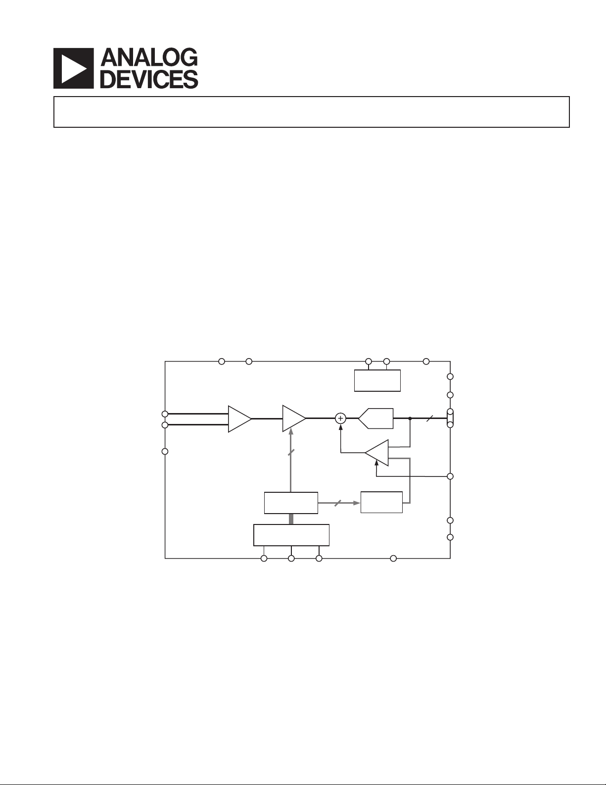
FUNCTIONAL BLOCK DIAGRAM
AV DD
AVSS
AD9821
0dB ~ 36dB
VIN+
VIN–
+
SHA
–
VGA
GENERAL DESCRIPTION
The AD9821 is a complete analog signal processor for imaging
applications that do not require Correlated Double Sampling
(CDS). It features a 40 MHz single-channel architecture designed
to sample and condition the outputs of CMOS imagers and CCD
arrays already containing on-chip CDS. The AD9821’s signal
chain consists of a differential input sample-and-hold amplifier
(SHA), digitally controlled variable gain amplifier (VGA), black
level clamp, and a 12-bit ADC.
The internal registers are programmed through a 3-wire serial
digital interface. Programmable features include gain adjustment, black level adjustment, and power-down modes.
The AD9821 operates from a single 3 V power supply, typically
dissipates 150 mW, and is packaged in a 48-lead LQFP.
PBLKVRT VRB
BAND GAP
REFERENCE
12-BIT
ADC
DRVDD
DRVSS
12
DOUT
BYP1
SL
10
INTERNAL
REGISTERS
DIGITAL
INTERFACE
REV. 0
Information furnished by Analog Devices is believed to be accurate and
reliable. However, no responsibility is assumed by Analog Devices for its
use, nor for any infringements of patents or other rights of third parties that
may result from its use. No license is granted by implication or otherwise
under any patent or patent rights of Analog Devices.
CLP
CLPOB
8
BLK CLAMP
LEVEL
DVD D
DVSS
SDATASCK
One Technology Way, P.O. Box 9106, Norwood, MA 02062-9106, U.S.A.
Tel: 781/329-4700www.analog.com
Fax: 781/326-8703 © Analog Devices, Inc., 2002
DATACLK
Page 2

AD9821–SPECIFICATIONS
to T
GENERAL SPECIFICATIONS
(T
MIN
, AVDD = DVDD = 3.0 V, f
MAX
Parameter Min Typ Max Unit
TEMPERATURE RANGE
Operating –20 +85 °C
Storage –65 +150 °C
POWER SUPPLY VOLTAGE
Analog, Digital, Digital Driver 2.7 3.6 V
POWER CONSUMPTION
Normal Operation (Specified under Each Mode of Operation)
Power-Down Modes
Standby 5 mW
Total Power-Down 1 mW
MAXIMUM CLOCK RATE 40 MHz
A/D CONVERTER
Resolution 12 Bits
Differential Nonlinearity (DNL) ± 0.5 LSB
No Missing Codes 12 Bits Guaranteed
Full-Scale Input Voltage 2.0 V
Data Output Coding Straight Binary
VOLTAGE REFERENCE
Reference Top Voltage (VRT) 2.0 V
Reference Bottom Voltage (VRB) 1.0 V
Specifications subject to change without notice.
= 40 MHz, unless otherwise noted.)
DATACLK
DIGITAL SPECIFICATIONS
(DRVDD = 2.7 V, CL = 20 pF, unless otherwise noted.)
Parameter Symbol Min Typ Max Unit
LOGIC INPUTS
High Level Input Voltage V
Low Level Input Voltage V
High Level Input Current I
Low Level Input Current I
Input Capacitance C
IH
IL
IH
IL
IN
2.1 V
0.6 V
10 µA
10 µA
10 pF
LOGIC OUTPUTS
High Level Output Voltage, IOH = 2 mA V
Low Level Output Voltage, IOL = 2 mA V
Specifications subject to change without notice.
OH
OL
2.2 V
0.5 V
REV. 0–2–
Page 3
AD9821
IMAGER-MODE SPECIFICATIONS
(T
to T
MIN
, AVDD = DVDD = 3.0 V, f
MAX
= 40 MHz, unless otherwise noted.)
DATACLK
Parameter Min Typ Max Unit Notes
P
OWER CONSUMPTION 150 mW See TPC 1 for Power vs. Sample Rate
MAXIMUM CLOCK RATE 40 MHz
ANALOG INPUTS (VIN+, VIN–)
Input Common-Mode Range* 0 1.8 V Linear operating range for VIN+, VIN–
Max Input Amplitude* 1.0 V p-p Defined as VIN+ minus VIN–
Max Optical Black Pixel Amplitude* ± 30 mV For stable Clamp at max VGA gain
VARIABLE GAIN AMPLIFIER (VGA)
Gain Control Resolution 1024 Steps
Gain Monotonicity Guaranteed
Gain Range See Figure 11 for VGA Gain Curve
Min Gain (VGA Gain Code 00) 0 dB
Max Gain (VGA Gain Code 1023) 36 dB
BLACK LEVEL CLAMP
Clamp Level Resolution 256 Steps
Clamp Level Measured at ADC Output
Min Clamp Level 0 LSB
Max Clamp Level 255 LSB
SYSTEM PERFORMANCE Specifications Include Entire Signal Chain
Gain Accuracy
Min Gain –1 0 +1 dB
Max Gain 34.5 35.5 36.5 dB
Peak Nonlinearity, 500 mV Input 0.3 % 12 dB Gain Applied
Total Output Noise 0.5 LSB rms AC Grounded Input, 6 dB Gain Applied
Power Supply Rejection (PSR) 40 dB Measured with Step Change on Supply
POWER-UP RECOVERY TIME Normal Clock Signals Applied
Reference Standby Mode 1 ms
Total Power-Down Mode 3 ms
Power-Off Condition 10 ms
*Input Signal Characteristics defined as follows:
+1.8V
VIN+
VIN–
GND
Specifications subject to change without notice.
1V p-p MAX
INPUT SIGNAL RANGE
ⴞ30mV MAX
OB PIXEL
INPUT
CM RANGE
REV. 0
–3–
Page 4
AD9821
TIMING SPECIFICATIONS
(CL = 20 pF, f
= 40 MHz, Imager-Mode Timing in Figures 5 and 6, Serial Timing in Figures 7–9)
SAMP
Parameter Symbol Min Typ Max Unit
SAMPLE CLOCKS
DATACLK Clock Period t
DATACLK Hi/Low Pulsewidth t
CLPOB Pulsewidth* t
Internal Clock Delay t
CONV
ADC
COB
ID
25 25 ns
11 12.5 ns
220 Pixels
3.0 ns
DATA OUTPUTS
Output Delay t
Output Hold Time t
OD
H
7.0 7.6 ns
13 16 ns
Pipeline Delay 9 Cycles
SERIAL INTERFACE
Maximum SCK Frequency f
SL to SCK Setup Time t
SCK to SL Hold Time t
SDATA Valid to SCK Rising Edge Setup t
SCK Falling Edge to SDATA Valid Hold t
SCK Falling Edge to SDATA Valid Read t
*Minimum CLPOB pulsewidth is for functional operation only. Wider typical pulses are recommended to achieve low noise clamp performance.
Specifications subject to change without notice.
ABSOLUTE MAXIMUM RATINGS
With
Respect
Parameter To Min Max Unit
SCLK
LS
LH
DS
DH
DV
AVDD1, AVDD2 AVSS –0.3 +3.9 V
DVDD1, DVDD2 DVSS –0.3 +3.9 V
10 MHz
10 ns
10 ns
10 ns
10 ns
10 ns
ORDERING GUIDE
Temperature Package Package
Model Range Description Option
AD9821KST –20°C to +85°CThin Plastic ST-48
Quad Flatpack
(LQFP)
DRVDD DRVSS –0.3 +3.9 V
Digital Outputs DRVSS –0.3 DRVDD + 0.3 V
DATACLK DVSS –0.3 DVDD + 0.3 V
CLPOB, PBLK DVSS –0.3 DVDD + 0.3 V
SCK, SL, SDATA DVSS –0.3 DVDD + 0.3 V
VRT, VRB AVSS –0.3 AVDD + 0.3 V
THERMAL CHARACTERISTICS
Thermal Resistance
48-Lead LQFP Package
= 56°C/W
θ
JA
BYP1, VIN AVSS –0.3 AVDD + 0.3 V
Junction Temperature 150 °C
Lead Temperature 300 °C
(10 sec)
CAUTION
ESD (electrostatic discharge) sensitive device. Electrostatic charges as high as 4000 V readily
accumulate on the human body and test equipment and can discharge without detection. Although the
AD9821 features proprietary ESD protection circuitry, permanent damage may occur on devices
subjected to high energy electrostatic discharges. Therefore, proper ESD precautions are recommended
to avoid performance degradation or loss of functionality.
REV. 0–4–
Page 5
AD9821
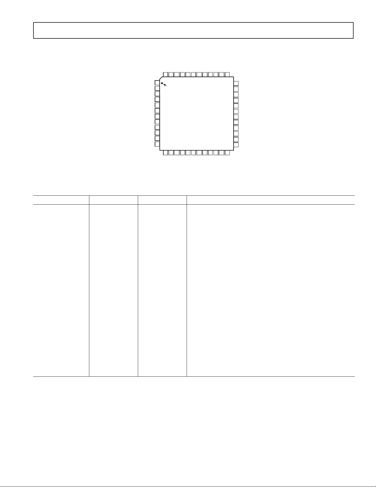
PIN CONFIGURATION
NCNCSCK
(LSB) D0
D1
D2
D3
D4
D5
D6
D7
D8
D9
D10
(MSB) D11
NC = NO CONNECT
48 47 46 4 5 44 39 38 3743 4 2 41 40
1
2
3
4
5
6
7
8
9
10
11
12
13 14 15 16 17 18 19 20 21 22 23 24
PIN 1
IDENTIFIER
DVSS
DRVSS
DRVDD
SDATASLSTBYNCDVSS
AD9821
TOP VIEW
(Not to Scale)
DVDD1
DATACLK
PIN FUNCTION DESCRIPTIONS
Pin Number Mnemonic Type Description
1–12 D0–D11 DO Digital Data Outputs
13 DRVDD P Digital Output Driver Supply
14 DRVSS P Digital Output Driver Ground
15, 41 DVSS P Digital Ground
16 DATACLK DI Digital Data Output Latch Clock
17 DVDD1 P Digital Supply
18, 24, 37, 42, 47, 48 NC NC Internally Not Connected. May be Tied High or Low.
19 PBLK DI Preblanking Clock Input
20 CLPOB DI Black Level Clamp Clock Input
21–23 TEST DI Test Use Only. Tie to VDD or VSS.
25, 26, 35 AVSS P Analog Ground
27 AVDD1 P Analog Supply
28, 29 TEST AO Test Use Only. Tie to VDD or VSS.
30 VIN+ AI Positive Analog Input for Imager Signal
31 VIN– AI Negative Analog Input for Imager Signal
32 BYP1 AO Internal Bias Level Decoupling
33 AVDD2 P Analog Supply
34, 36 TEST AI Test Use Only. Tie to VDD or VSS.
38 VRT AO ADC Top Reference Voltage Decoupling
39 VRB AO ADC Bottom Reference Voltage Decoupling
40 DVDD2 P Digital Supply
43 STBY DI Standby Mode, Active High. Same as Total Power-Down Mode.
44 SL DI Serial Digital Interface Load Pulse
45 SDATA DI Serial Digital Interface Data
46 SCK DI Serial Digital Interface Clock
TYPE: AI = Analog Input, AO = Analog Output, DI = Digital Input, DO = Digital Output, P = Power.
NC
PBLK
DVDD2
TEST
CLPOB
VRB
TEST
VRT
TEST
NC
NC
36
35
34
33
32
31
30
29
28
27
26
25
TEST
AVSS
TEST
AVDD2
BYP1
VIN–
VIN+
TEST
TEST
AVDD1
AVSS
AVSS
REV. 0
–5–
Page 6

AD9821
DEFINITIONS OF SPECIFICATIONS
Differential Nonlinearity (DNL)
An ideal ADC exhibits code transitions that are exactly 1 LSB
apart. DNL is the deviation from this ideal value. Thus, every
code must have a finite width. No missing codes guaranteed to
12-bit resolution indicates that all 4096 codes, respectively,
must be present over all operating conditions.
Peak Nonlinearity
Peak nonlinearity, a full signal chain specification, refers to the
peak deviation of the output of the AD9821 from a true straight
line. The point used as “zero scale” occurs 1/2 LSB before the
first code transition. “Positive full scale” is defined as a Level 1,
1/2 LSB beyond the last code transition. The deviation is measured from the middle of each particular output code to the true
straight line. The error is then expressed as a percentage of the
2 V ADC full-scale signal. The input signal is always appropriately
gained up to fill the ADC’s full-scale range.
EQUIVALENT INPUT CIRCUITS
DVDD
Total Output Noise
The rms output noise is measured using histogram techniques.
The standard deviation of the ADC output codes is calculated
in LSB and represents the rms noise level of the total signal
chain at the specified gain setting. The output noise can be
converted to an equivalent voltage using the relationship 1 LSB =
(ADC Full Scale/2
N
codes) when N is the bit resolution of the ADC.
For the AD9821, 1 LSB is 500 µV.
Power Supply Rejection (PSR)
The PSR is measured with a step change applied to the supply
pins. This represents a very high frequency disturbance on the
AD9821’s power supply. The PSR specification is calculated
from the change in the data outputs for a given step change in
the supply voltage.
Internal Delay for SHA
The internal delay (also called aperture delay) is the time delay
that occurs from when the sampling edge is applied to the AD9821
until the actual sample of the input signal is held. The DATACLK
samples the input signal during the transition from low to high,
so the internal delay is measured from each clock’s rising edge
to the instant the actual internal sample is taken.
330⍀
DVSS
Figure 1. Digital Inputs— DATACLK, CLPOB, PBLK, SCK, SL
DRVDD
DOUT
DATA
THREE-
STATE
DVDD
RNW
AV DD
60⍀
ACVSS
ACVSS
Figure 3. VIN+ and VIN– (Pins 30 and 31)
DVDD
DATA IN
DATA OUT
DVD D
330⍀
DVSS
Figure 2. Data Outputs—D0–D11
DRVSS
DVSS
DVSS
Figure 4. SDATA (Pin 47)
DVSS
REV. 0–6–
Page 7

160
0
VGA GAIN CODE – LSB
15.0
0 1023511
OUTPUT NOISE – LSB
255 767
13.5
12.0
10.5
9.0
7.5
6.0
4.5
3.0
1.5
150
Typical Performance Characteristics–
AD9821
140
130
120
POWER DISSIPATION – mW
110
100
20 4030
SAMPLE RATE – MHz
VDD = 3.0V
TPC 1. Power vs. Sample Rate
1.0
0.5
0
–0.5
–1.0
0 500 1000 1500 2000 2500 3000 35000 4000
TPC 3. Output Noise vs. VGA Gain
REV. 0
TPC 2. Typical DNL Performance
–7–
Page 8

AD9821
IMAGER MODE AND AUX MODE TIMING
N
VIN+
t
VIN–
DATACLK
t
OD
OUTPUT
DATA
NOTES:
1. VIN+ AND VIN– SIGNALS ARE SAMPLED AT DATACLK RISING EDGES (CAN BE INVERTED USING THE CONTROL REGISTER).
2. INTERNAL SAMPLING DELAY (APERTURE)
3. OUTPUT DATA LATENCY IS NINE DATACLK CYCLES.
N–10 N–9 N–8 N–1 N
ID
N+1
t
H
t
IS TYPICALLY 3 ns.
ID
t
CONV
N+2
N+8
Figure 5. Imager Mode Timing
HORIZONTAL
BLANKING
IMAGER
SIGNAL
CLPOB
EFFECTIVE PIXELS
OPTICAL BLACK PIXELS
N+9
EFFECTIVE PIXELS
PBLK
OUTPUT
DATA
EFFECTIVE PIXEL DATA
NOTES:
1. CLPOB WILL OVERWRITE PBLK. PBLK WILL NOT AFFECT CLAMP OPERATION IF OVERLAPPING CLPOB.
2. PBLK SIGNAL IS OPTIONAL.
3. DIGITAL OUTPUT DATA WILL BE ALL ZEROS DURING PBLK. OUTPUT DATA LATENCY IS NINE DATACLK CYCLES.
OB PIXEL DATA EFFECTIVE DATA
Figure 6. Typical Imager Mode Line Clamp Timing
REV. 0–8–
Page 9

AD9821
INTERNAL REGISTER MAP AND SERIAL INTERFACE TIMING
Table I. Internal Register Map
Register Address Data Bits
Name A0 A1 A2 D0 D1 D2 D3 D4 D5 D6 D7 D8 D9 D10
Operation 0 0 0 Input Mode Power-Down Software OB Clamp 0
1
Selection Modes Reset On/Off
VGA Gain 1 0 0 LSB MSB X
Clamp Level 0 1 0 LSB MSB X X X
Control 1 1 0 0
1
1
0
1
0
1
0
1
0
Clock Polarity Select for 0
CLP/DATA
NOTES
1
Internal use only. Must be set to 0.
2
Must be set to 1.
RNW TEST BIT
SDATA
SCK
0
t
DS
t
DH
A2 0A0 A1 D0 D1 D2 D3 D4 D5 D6 D7 D8 D9 D10
2
1
1
1
0
1
0
1
0
1
0
1
0
X
SDATA
t
LS
SL
NOTES:
1. SDATA BITS ARE INTERNALLY LATCHED ON THE RISING EDGES OF SCK.
2. RNW = READ-NOT WRITE. SET LOW FOR WRITE OPERATION.
3. TEST BITS = INTERNAL USE ONLY. MUST BE SET LOW.
4. SYSTEM UPDATE OF LOADED REGISTERS OCCURS ON SL RISING EDGE.
Figure 7. Serial Write Operation
RNW TEST BIT
10
SDATA
t
DS
SCK
SL
NOTES:
1. RNW = READ-NOT WRITE. SET HIGH FOR READ OPERATION.
2. TEST BITS = INTERNAL USE ONLY. MUST BE SET LOW.
3. SERIAL DATA FROM THE SELECTED REGISTER IS VALID STARTING AFTER THE FIFTH SCK FALLING EDGE, AND IS UPDATED ON
SCK FALLING EDGES.
A0 A1 D0 D1 D2 D3 D4 D5 D6 D7 D8 D9 D10
t
DH
t
LS
0
t
DV
Figure 8. Serial Readback Operation
RNW
A0
A1 A2
000
11 BITS
OPERATION
00
D0
D2
D1
...
D3 D10
D0
D1
10 BITS
VGA GAIN
D3D2
...
D9
D0
8 BITS
CLAMP LEVEL
D1
D2
...
D3 D7 D0 D3
t
LH
t
LH
CONTROL
D1
10 BITS
D2
...
D9
SCK
292019171686543 26 27 30 3837353429 44
1
SL
NOTES:
1. ANY NUMBER OF ADJACENT REGISTERS MAY BE LOADED SEQUENTIALLY, BEGINNING WITH THE LOWEST ADDRESS AND INCREMENTING ONE ADDRESS AT A TIME.
2. WHEN SEQUENTIALLY LOADING MULTIPLE REGISTERS, THE EXACT REGISTER LENGTH (SHOWN ABOVE) MUST BE USED FOR EACH REGISTER.
3. ALL LOADED REGISTERS WILL BE SIMULTANEOUSLY UPDATED WITH THE RISING EDGE OF SL.
7182836
...
...
...
Figure 9. Continuous Serial Write Operation to All Registers
REV. 0
–9–
...
...
Page 10

AD9821
REGISTER DETAILS
Table II. Operation Register Contents (Default Value x000)
Optical Black Clamp Reset Power-Down Modes Channel Selection
D10 D9 D8 D7 D6 D5 D4 D3 D2 D1 D0
1
0
010112 010 Enable Clamping 0 Normal 0 0 Normal Power 0 0 Test Only
1 Disable Clamping 1 Reset All Registers 0 1 Test Only 0 1 Test Only
to Default 1 0 Ref-Standby 1 0 Test Only
11Total Power-Down 1 1 Imager Mode
NOTES
1
Must be set to 0.
2
Set to 1.
Table III. VGA Gain Register Contents (Default Value x000)
MSB LSB
D10 D9 D8 D7 D6 D5 D4 D3 D2 D1 D0 Gain (dB)
X0 0 000000000.0
••
••
••
11 1111111035.965
11 1111111136.0
Table IV. Clamp Level Register Contents (Default Value x080)
MSB LSB
D10 D9 D8 D7 D6 D5 D4 D3 D2 D1 D0 Clamp Level (LSB)
X XX0000 0000 0
0000 0001 1
0000 0010 2
••
••
••
11111110 254
11111111 255
Table V. Control Register Contents (Default Value x000)
DATACLK Polarity CLPOB/PBLK Polarity
D10 D9 D8 D7 D6 D5 D4 D3 D2 D1 D0
X0* 0* 0* 0 Sample on Rising Edge 0 Active Low 0* 0* 0* 0* 0*
1 Sample on Falling Edge 1 Active High
*Must be set to 0.
REV. 0–10–
Page 11

AD9821
CIRCUIT DESCRIPTION AND OPERATION
The AD9821 signal processing chain is shown in Figure 10.
Each processing step is essential in achieving a high quality
image from the raw imager pixel data.
Differential Input SHA
The differential input SHA circuit is designed to accommodate
a variety of different image sensor output voltages. The timing
shown in Figure 8 illustrates how the DATACLK signal is used to
sample both the VIN+ and VIN– signals simultaneously. The
imager signal is sampled on the rising edges of DATACLK.
Placement of this clock signal is critical in achieving the best
performance from the imager. An internal DATACLK delay (t
)
ID
of 3 ns is caused by internal propagation delays.
The differential input can be used in a variety of single-ended
and differential configurations, as shown in Table VI. The
allowable voltage range for both VIN+ or VIN– is from 0 V
to 1.8 V. Signal levels outside this range will result in severely
degraded performance. Regardless of the input configuration,
the voltage sampled by the SHA is always equal to VIN+ minus
VIN–. VIN+ must always be equal to or greater than VIN– or
DATACLK
0dB TO 36dB
VIN+
VIN–
SHA
VGA
negative clipping will occur. A small amount of offset between
the VIN+ and VIN– signals is allowable and can be corrected by
the Optical Black Clamp, up to ±30 mV.
Note that the VIN+ and VIN– inputs do not contain any dc
restoration or bias circuitry. Therefore, dc-coupling is recommended when driving the AD9821 analog inputs. If ac-coupling is
used, external biasing circuitry must be provided for the VIN+
and VIN– inputs to keep them in the acceptable common-mode
voltage range of 0 V to 1.8 V.
Table VI. Example Input Voltage Configurations
VIN+ Range (V) VIN– Range (V) SHA Output Range (V)
Black White Black White Black White
0 1.0 0 0 0 1.0
0.5 1.5 0.5 0.5 0 1.0
1.0 1.5 1.0 0.5 0 1.0
0.5 1.0 0.5 0 0 1.0
1.0 1.0 1.0 0 0 1.0
1.0F 1.0F
12-BIT
ADC
REFB
1.0V
INTERNAL
VREF
REFT
2.0V
PBLK
12
DOUT
BYP1
0.1F
0.45V
INTERNAL
BIAS
10
VGA GAIN
REGISTER
8-BIT
DAC
OPTICAL BLACK
CLAMP
DIGITAL
FILTERING
Figure 10. Internal Block Diagram
8
CLAMP LEVEL
REGISTER
CLPOB
REV. 0
–11–
Page 12

AD9821
Variable Gain Amplifier
The VGA stage provides a gain range of 0 dB to 36 dB, programmable with 10-bit resolution through the serial digital interface. A
minimum gain of 6 dB is needed to match a 1 V input signal with
the ADC full-scale range of 2 V. When compared to 1 V full-scale
systems, the equivalent gain range is –6 dB to +30 dB.
The VGA gain curve follows a “linear-in-dB” characteristic.
The exact VGA gain can be calculated for any Gain Register
value by using the equation:
Gain dB Code()(. )=×0 0351
where the code range is 0 to 1023.
36
30
24
18
VGA GAIN – dB
12
6
0
127 255 383 511 639 767 895 1023
0
VGA GAIN REGISTER CODE
Figure 11. VGA Gain Curve
Optical Black Clamp
The optical black clamp loop is used to remove residual offsets
in the signal chain, and to track low frequency variations in the
CCD’s black level. During the optical black (shielded) pixel
interval on each line, the ADC output is compared with a fixed
black level reference selected by the user in the Clamp Level
Register. Any value between 0 LSB and 255 LSB may be
programmed using the 8-bit Clamp Level Register. The resulting
error signal is filtered to reduce noise, and the correction value is
applied to the ADC input through a D/A converter. Normally, the
optical black clamp loop is turned on once per horizontal line, but
this loop can be updated more slowly to suit a particular
application. If external digital clamping is used during the postprocessing, the AD9821 optical black clamping may be disabled
using Bit D5 in the Operation Register (see Internal Register
Map and Serial Interface Timing section). When the loop is
disabled, the Clamp Level Register may still be used to provide
programmable offset adjustment.
Horizontal timing is shown in Figure 9. The CLPOB pulse
should be placed during the CCD’s optical black pixels. It is
recommended that the CLPOB pulse duration be at least 20
pixels wide. Shorter pulsewidths may be used, but the ability to
track low frequency variations in the black level will be reduced.
As discussed in the Differential Input SHA section, the CLPOB
loop is capable of correcting for an offset difference between the
VIN+ and VIN– inputs. Because the clamp is located after the
VGA gain stage, the clamp will be most limited when the VGA
gain is at its maximum value. Under these conditions, the OB
clamp loop correction range is restricted to ±30 mV offset
between the VIN+ and VIN– inputs. At minimum VGA gain,
the offset correction range increases to ±250 mV of offset. If the
OB clamp loop’s correction range is exceeded, then the black
level at the output of the AD9821 will increase and further
correction will be necessary. As mentioned previously, it is also
possible to disable the AD9821’s OB clamp loop.
A/D Converter (ADC)
The AD9821 uses high performance ADC architecture, optimized for high speed and low power. Differential nonlinearity
(DNL) performance is typically better than 0.5 LSB, as shown in
TPC 2. Instead of the 1 V full-scale range used by the earlier
AD9801 and AD9803 products from Analog Devices, the
AD9821’s ADC uses a 2 V input range. Better noise performance
results from using a larger ADC full-scale range (see TPC 3).
REV. 0–12–
Page 13

AD9821
APPLICATIONS INFORMATION
The AD9821 is a complete Analog Front End (AFE) product
for a variety of imager applications using CMOS image sensors
and CCDs with on-chip CDS. As shown in Figure 10, the imager
output is generally buffered and sent to the AD9821’s analog
inputs, either as a differential or single-ended signal. The AD9821
performs the sample-and-hold operation, gain adjustment,
black level correction, and analog-to-digital conversion. The
CMOS
OR
CCD
IMAGER
V- DRIVE
(CCD)
OUT+
OUT–
BUFFER
OR
LEVEL SHIFT
IMAGER
TIMING
AD9821
VIN+
VIN–
GENERATOR
Figure 12. System Applications Diagram
3V
ANALOG SUPPLY
AD9821’s digital output data is then processed by the image
processing ASIC. The internal registers of the AD9821—used
to control gain, offset level, and other functions—are
programmed by the ASIC or microprocessor through a 3-wire
serial digital interface. A system timing generator provides the
clock signals for both the imager and the AFE.
ADC
REGISTER-
DATA
DATACL K/CLAMP
TIMING
TIMING
0.1F
OUT
DIGITAL
OUTPUTS
SERIAL
INTERFACE
DIGITAL IMAGE
PROCESSING
ASIC
(MAY ALSO
INCLUDE TG)
DATA
OUTPUTS
1.0F
SERIAL
INTERFACE
D0
D1
D2
D3
D4
D5
D6
D7
D8
D9
D10
(MSB) D11
12
3V
DRIVER
SUPPLY
3
SCK
SDATA
SLNCSTBY
NC
1
PIN 1
2
IDENTIFIER
3
4
5
6
7
8
9
10
11
12
13 14 15 16 17 18 19 20 21 22 23 24
DVSS
DRVSS
DRVDD
0.1F
AD9821
TOP VIEW
(Not to Scale)
NC
DVDD1
DATACLK
NC
PBLK
DVSS
DVDD2
TEST
CLPOB
VRB
TEST
VRT
TEST
3
NC
3748 47 46 45 44 39 3843 42 41 40
NC
1.0F
36
35
34
33
32
31
30
29
28
27
26
25
CLOCK
INPUTS
TEST
AVSS
TEST
AVDD2
BYP1
VIN-
VIN+
TEST
TEST
AVDD1
AVSS
AVSS
0.1F
0.1F
0.1F
NC = INTERNALLY NOT CONNECTED
3V
ANALOG SUPPLY
IMAGER INPUT, NEGATIVE/REFERENCE
IMAGER INPUT, POSITIVE
3V
ANALOG SUPPLY
REV. 0
0.1F
3V
ANALOG SUPPLY
Figure 13. Recommended Circuit Configuration
–13–
Page 14

AD9821
Internal Power-On Reset Circuitry
After power-on, the AD9821 will automatically reset all internal
registers and perform internal calibration procedures. This takes
approximately 1 ms to complete. During this time, normal clock
signals and serial write operations may occur. However, serial
register writes will be ignored until the internal reset operation
is completed.
Grounding and Decoupling Recommendations
As shown in Figure 13, a single ground plane is recommended
for the AD9821. This ground plane should be as continuous as
possible, particularly around Pins 25 through 39. This will ensure
that all analog decoupling capacitors provide the lowest possible
impedance path between the power and bypass pins and their
respective ground pins. All decoupling capacitors should be
located as close as possible to the package pins. A single clean
power supply is recommended for the AD9821, but a separate
digital driver supply may be used for DRVDD (Pin 13). DRVDD
should always be decoupled to DRVSS (Pin 14), which should
be connected to the analog ground plane. Advantages of using a
separate digital driver supply include using a lower voltage (2.7 V)
to match levels with a 2.7 V ASIC, reducing digital power
dissipation, and reducing potential noise coupling. If the
digital outputs (Pins 1–12) must drive a load larger than 20 pF,
buffering is recommended to reduce digital code transition noise.
Alternatively, placing series resistors close to the digital output
pins may also help reduce noise.
REV. 0–14–
Page 15

OUTLINE DIMENSIONS
48-Lead Plastic Quad Flatpack [LQFP]
1.4 mm Thick
(ST-48)
Dimensions shown in millimeters
AD9821
1.45
1.40
1.35
0.15
0.05
SEATING
PLANE
ROTATED 90ⴗ CCW
VIEW A
0.08 MAX
COPLANARITY
1.60 MAX
0.75
0.60
0.45
SEATING
PLANE
0.20
0.09
7ⴗ
3.5ⴗ
0ⴗ
COMPLIANT TO JEDEC STANDARDS MS-026BBC
PIN 1
INDICATOR
VIEW A
1
12
0.50
BSC
48
13
9.00 BSC
TOP VIEW
(PINS DOWN)
24
37
36
25
0.27
0.22
0.17
7.00
BSC
REV. 0
–15–
Page 16

C03223–0–11/02(0)
–16–
PRINTED IN U.S.A.
 Loading...