

Page 1
Complete 12-Bit 6 MSPS
a
FEATURES
12-Bit 6 MSPS A/D Converter
No Missing Codes Guaranteed
3-Channel or 1-Channel Operation
Correlated Double Sampling
8-Bit Programmable Gain
8-Bit Offset Adjustment
PGA Output Monitor
Input Clamp Circuitry
Internal Voltage Reference
3-Wire Serial Interface
+3.3 V/+5 V Digital Output Compatibility
44-Lead MQFP Package
Low Power CMOS: 420 mW Typ
AVDD AVSS
PRODUCT DESCRIPTION
The AD9816 is a complete analog signal processor for CCD
and CIS applications. Included is all the necessary circuitry to
perform three-channel conditioning and sampling for a variety
of imaging applications.
The signal chain consists of an input clamp, correlated double
sampler (CDS), offset adjust DAC, programmable gain amplifier and a 12-bit A/D converter. The CDS and input clamp may
be disabled for CIS applications.
The internal registers are programmed using a 3-wire serial
interface and provide adjustment of the gain, offset and operating mode.
The AD9816 operates from a +5 V supply, typically consumes
420 mW of power and is packaged in a 44-lead MQFP.
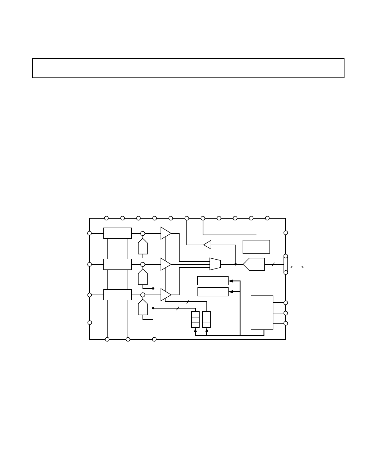
FUNCTIONAL BLOCK DIAGRAM
CAPT CAPB CML PGAOUT VREF
CCD/CIS Signal Processor
AD9816
DVDD DVSS DRVDD DRVSS
VINR
VING
VINB
OFFSET
CLAMP/CDS
CLAMP/CDS
CLAMP/CDS
CDSCLK1
6100mV
+
DAC
+
DAC
+
DAC
OFFSET
REGISTERS
CDSCLK2 ADCCLK
1X–6X
PGA
PGA
PGA
AD9816
OEB
BANDGAP
REFERENCE
ADC
DIGITAL
CONTROL
PORT
12
DOUT
11:0
SCLK
SLOAD
SDATA
MUX
MUX
REGISTER
CONFIGURATION
R
G
B
REGISTER
R
G
REGISTERS
B
GAIN
8
8
12-BIT
REV. A
Information furnished by Analog Devices is believed to be accurate and
reliable. However, no responsibility is assumed by Analog Devices for its
use, nor for any infringements of patents or other rights of third parties
which may result from its use. No license is granted by implication or
otherwise under any patent or patent rights of Analog Devices.
One Technology Way, P.O. Box 9106, Norwood, MA 02062-9106, U.S.A.
Tel: 781/329-4700 World Wide Web Site: http://www.analog.com
Fax: 781/326-8703 © Analog Devices, Inc., 1998
Page 2

AD9816–SPECIFICATIONS
(T
to T
ANALOG SPECIFICATIONS
f
CDSCLK1
= 2 MHz, f
= 2 MHz, PGA Gain = 1, Input Range = 3 V p-p, Input Capacitor = 1200 pF, unless otherwise noted)
CDSCLK2
MIN
with AVDD = +5.0 V, DVDD = +5.0 V, DRVDD = +5.0 V, CDS Mode, f
MAX
Parameter AD9816 AD9816-80010 Units
MAXIMUM CONVERSION RATE
3-Channel Mode with CDS 6 6 MSPS min
1-Channel Mode with CDS 6 6 MSPS min
ACCURACY (Includes Entire Signal Path)
ADC Resolution 12 12 Bits min
Differential Nonlinearity (DNL) ±0.4 ±0.75 LSB typ
±1.0 LSB max
No Missing Codes 12 Bits Guaranteed
Integral Nonlinearity (INL) ±1.5 ±2.5 LSB typ
±4.0 LSB max
Offset Error 2.4 % FSR max
Gain Error
ANALOG INPUTS
Input Voltage Range
Input Limits
1
2
3
4.3 % FSR max
0 0 V min
3 3 V max
AVSS – 0.3 AVSS – 0.3 V min
AVDD + 0.3 AVDD + 0.3 V max
Input Capacitance 10 10 pF typ
Input Current 10 10 nA typ
AMPLIFIERS
PGA Gain Range 1 1 V/V min
5.98 5.98 V/V max
PGA Gain Resolution 256 256 Steps
Offset Range –100 –100 mV min
+100 +100 mV max
Offset Resolution 256 256 Steps
NOISE AND CROSSTALK
Total Output Noise at Min PGA Gain
Total Output Noise at Max PGA Gain
Channel-to-Channel Crosstalk
5
4
4
0.5 LSB rms typ
0.8 LSB rms typ
1LSB max
POWER SUPPLY REJECTION
(AVDD = +5 V/±0.25 V) 0.28 % FSR max
VOLTAGE REFERENCE
0.75 V Reference Tolerance (@ +25°C) ±20 mV max
1.5 V Reference Tolerance (@ +25°C) ±34 mV max
TEMPERATURE RANGE
Operating 0 0 °C min
+70 +70 °C max
POWER SUPPLIES
Operating Voltages
AVDD, DVDD +4.75 +4.75 V min
+5.25 +5.25 V max
DRVDD +3.3 +3.3 V min
+5.25 +5.25 V max
Operating Current 84 84 mA typ
POWER CONSUMPTION 420 420 mW typ
500 500 mW max
NOTES
1
Includes internal voltage reference error.
2
Input voltage range is the linear region over which the input signal can be processed by the input stage of the AD9816.
3
The input limits are defined as the maximum tolerable input voltage into the AD9816. This is not intended to be the linear input range of the device. Signals beyond
the input limits will turn on the overvoltage protection diodes.
4
The total output noise is measured with the inputs of the AD9816 grounded.
5
The channel-to-channel crosstalk is measured with one input grounded, and the other two inputs at full scale.
Specifications subject to change without notice.
ADCCLK
= 6 MHz,
–2–
REV. A
Page 3

AD9816
(T
to T
DIGITAL SPECIFICATIONS
f
CDSCLK1
= 2 MHz, f
= 2 MHz, CL = 10 pF unless otherwise noted)
CDSCLK2
MIN
with AVDD = +5.0 V, DVDD = +5.0 V, DRVDD = +5.0 V, f
MAX
Parameter Symbol Min Typ Max Units
LOGIC INPUTS
High Level Input Voltage V
Low Level Input Voltage V
High Level Input Current I
Low Level Input Current I
Input Capacitance C
IH
IL
IH
IL
IN
3.5 V
10 µA
10 µA
10 pF
LOGIC OUTPUTS
High Level Output Voltage V
Low Level Output Voltage V
High Level Output Current I
Low Level Output Current I
Specifications subject to change without notice.
(T
TIMING SPECIFICATIONS
MIN
to T
OH
OL
OH
OL
with DVDD = +5.0 V, DRVDD = +5.0 V)
MAX
4.5 V
50 µA
50 µA
Parameter Symbol Min Typ Max Units
CLOCK PARAMETERS
3-Channel Conversion Rate t
1-Channel Conversion Rate t
ADCCLK Pulsewidth t
CDSCLK1 Pulsewidth t
CDSCLK2 Pulsewidth t
CDSCLK1 Falling to CDSCLK2 Rising t
ADCCLK Falling to CDSCLK2 Rising t
CDSCLK2 Falling to ADCCLK Falling t
CDSCLK2 Falling to CDSCLK1 Rising t
Aperture Delay for CDS Clocks t
CRA
CRB
ADCLK
C1
C2
C1C2
ADC2
C2AD
C2C1
AD
500 ns
160 ns
80 ns
20 ns
60 2 t
ADCLK
5ns
0ns
30 ns
10 ns
10 ns
SERIAL INTERFACE
Maximum SCLK Frequency f
SLOAD to SCLK Set-Up Time t
SCLK to SLOAD Hold Time t
SDATA to SCLK Rising Set-Up Time t
SCLK Rising to SDATA Hold Time t
SCLK Falling to SDATA Valid t
SCLK
LS
LH
DS
DH
RDV
10 MHz
10 ns
10 ns
10 ns
10 ns
10 ns
DATA OUTPUT
Output Delay t
3-State to Data Valid t
Output Enable High to 3-State t
OD
DV
HZ
13 ns
15 ns
5ns
Latency (Pipeline Delay) 3 (Fixed) ADCCLK Cycles
= 6 MHz,
ADCCLK
1.0 V
0.1 V
– 30 ns
–3–REV. A
Page 4
AD9816
ANALOG
INPUTS
CDSCLK1
CDSCLK2
ADCCLK
OUTPUT
DATA
D11:D0
PGAOUT_T
PGAOUT_C
ANALOG
INPUTS
CDSCLK2
ADCCLK
OUTPUT
DATA
D11:D0
PGAOUT_T
PGAOUT_C
PIXEL n (R, G, B)
t
AD
t
C1
t
ADCLK
t
ADCLK
R(n–2) G(n–2) B(n–2) R(n–1) G(n–1) B(n–1) R(n) G(n) B(n) R(n+1)
G(n–1) B(n–1) R(n) G(n) B(n) R(n+1) G(n+1)
t
ADC2
t
C1C2
t
AD
t
C2C1
t
C2
t
C2AD
PIXEL (n+1) PIXEL (n+m)
t
CRA
t
OD
PIXEL (n+2)
B(n+1)
R(n+2)
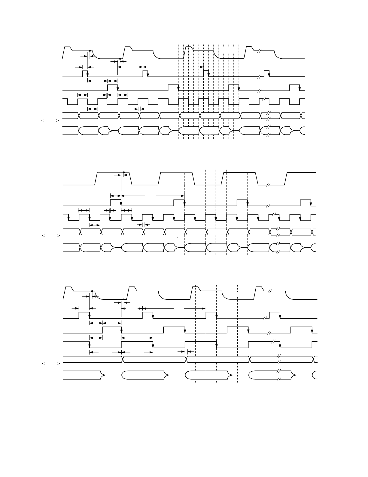
Figure 1. 3-Channel CDS Mode Timing
PIXEL n (R, G, B)
t
AD
t
C2
ADCLK
G(n–1)
t
ADC2
B(n–1)
t
ADCLK
t
R(n–2) G(n–2) B(n–2) R(n–1) G(n–1) B(n–1) R(n) G(n) B(n) R(n+1)
t
CRA
t
C2AD
t
OD
R(n) G(n) B(n) R(n+1) G(n+1)
PIXEL (n+2)PIXEL (n+1)
B(n+1)
R(n+2)
PIXEL (n+m)
ANALOG
INPUTS
CDSCLK1
CDSCLK2
ADCCLK
OUTPUT
DATA
D11:D0
PGAOUT_T
PGAOUT_C
Figure 2. 3-Channel SHA Mode Timing
t
AD
t
C1
t
C1C2
t
ADC2
PIXEL (n–4) PIXEL (n–3) PIXEL (n–2) PIXEL (n–1)
PIXEL (n–1) PIXEL n PIXEL (n+1)
PIXEL n PIXEL (n+m)
t
t
ADCLK
AD
t
C2C1
t
C2
t
C2AD
t
ADCLK
PIXEL (n+1)
t
CRB
t
OD
Figure 3. 1-Channel CDS Mode Timing
PIXEL (n+2)
PIXEL (n+2)
–4–
REV. A
Page 5
AD9816
ANALOG
INPUTS
CDSCLK2
ADCCLK
OUTPUT
DATA
,D11:D0.
PGAOUT_T
PGAOUT_C
ANALOG
INPUTS
CDSCLK1
CDSCLK2
PIXEL n PIXEL (n+m)
t
AD
t
C2
t
ADC2
t
PIXEL (n–4) PIXEL (n–3) PIXEL (n–2) PIXEL (n–1)
PIXEL (n–1) PIXEL n PIXEL (n+1) PIXEL (n+2)
ADCLK
t
C2AD
t
ADCLK
t
CRB
t
OD
PIXEL (n+2)PIXEL (n+1)
Figure 4. 1-Channel SHA Mode Timing
OPTICAL BLACK OR DUMMY PIXELS
EFFECTIVE PIXELS
ADCCLK
ADCCLK
OUTPUT
DATA
,D11:D0.
OEB
Figure 5. Line Clamp Timing for 3-Channel CDS Mode
t
OD
t
HZ
Figure 6. Output Enable Timing
t
DV
–5–REV. A
Page 6

AD9816
ABSOLUTE MAXIMUM RATINGS*
With
Respect
Parameter To Min Max Units
VIN, VREF AVSS –0.3 AVDD + 0.3 V
PGA Outputs AVSS –0.3 AVDD + 0.3 V
Clock Inputs DVSS –0.3 DVDD + 0.3 V
AVDD AVSS –0.5 +6.5 V
DVDD DVSS –0.5 +6.5 V
DRVDD DRVSS –0.5 +6.5 V
AVSS DVSS –0.3 +0.3 V
Digital Outputs DRVSS –0.3 DRVDD + 0.3 V
Digital Inputs DVSS –0.3 DVDD + 0.3 V
°
Junction Temperature +150
Storage Temperature –65 +150
Lead Temperature
(10 sec) +300
*Stresses above those listed under Absolute Maximum Ratings may cause perma-
nent damage to the device. This is a stress rating only; functional operation of the
device at these or other conditions above those indicated in the operational sections
of this specification is not implied. Exposure to absolute maximum ratings for
extended periods may affect device reliability.
C
°
C
°C
ORDERING GUIDE
Temperature Package Package
Model Range Description Option
AD9816JS 0°C to +70°C 44-Lead MQFP (Metric) Plastic Quad Flatpack S-44
AD9816JS-80010 0°C to +70°C 44-Lead MQFP (Metric) Plastic Quad Flatpack S-44
AD9816-EB Evaluation Board
CAUTION
ESD (electrostatic discharge) sensitive device. Electrostatic charges as high as 4000 V readily
accumulate on the human body and test equipment and can discharge without detection.
Although the AD9816 features proprietary ESD protection circuitry, permanent damage may
occur on devices subjected to high energy electrostatic discharges. Therefore, proper ESD
precautions are recommended to avoid performance degradation or loss of functionality.
WARNING!
ESD SENSITIVE DEVICE
–6–
REV. A
Page 7

AD9816
PIN 1
IDENTIFIER
TOP VIEW
(Not to Scale)
NC = NO CONNECT
DRVSS
DB5
DB4
DB3
DB2
DB1
DB0 (LSB)
DVSS
SLOAD
SDATA
SCLK
AVDD
AVSS
CAPT
CAPT
CAPB
CAPB
VREF
CML
VINR
AVSS
VING
PGAOUT_T
PGAOUT_CNCOEB
DB11(MSB)
DB10
DB9
AVSS
VINB
AVSS
AVDD
CDSCLK1
CDSCLK2
ADCCLK
DVSS
DVDD
NC
OFFSET
DB8
DB7
DB6
DRVDD
AD9816
3435363738394041424344
1
2
3
4
5
6
7
8
9
10
11
12 13 14 15 16 17 18 19 20 21 22
33
32
31
30
29
28
27
26
25
24
23
PIN FUNCTION DESCRIPTIONS
Pin Pin Name Type Description
1 AVDD P +5 V Analog Supply.
2 AVSS P Analog Ground.
3, 4 CAPT AO Reference Decoupling.
5, 6 CAPB AO Reference Decoupling.
7 VREF AO Internal Reference Output.
8 CML AO Internal Bias Level.
9 VINR AI Analog Input, Red Channel.
10 AVSS P Analog Ground.
11 VING AI Analog Input, Green Channel.
12 AVSS P Analog Ground.
13 VINB AI Analog Input, Blue Channel.
14 AVSS P Analog Ground.
15 AVDD P +5 V Analog Supply.
16 OFFSET AI Clamp bias level in CDS mode.
Offset adjustment input in SHA
mode.
17 CDSCLK1 DI CDS Reset Level Sampling
Clock.
18 CDSCLK2 DI CDS Data Level Sampling
Clock.
19 ADCCLK DI A/D Converter Sampling Clock.
20 DVSS P Digital Ground.
21 DVDD P +5 V Digital Supply.
22 NC No Connect.
23 SCLK DI Clock Input for Serial Interface.
24 SDATA DIO Serial Data Input-Output.
25 SLOAD DI Load Pulse for Serial Interface.
26 DVSS P Digital Ground.
27 DB0 DO Data Output (LSB).
28–32 DB1–DB5 DO Data Outputs.
33 DRVSS P Digital Driver Ground.
34 DRVDD P Digital Driver Supply.
35–39 DB6–DB10 DO Data Outputs.
40 DB11 DO Data Output (MSB).
41 OEB DI Output Enable, Active Low.
42 NC No Connect.
43 PGAOUT_C AO PGA Output, Negative. This
pin should be left unconnected
except during evaluation.
should be left unconnected
except during evaluation.
44 PGAOUT_T AO PGA Output, Positive. This pin
NOTES
See Applications Information for circuit configurations.
TYPE: AI = Analog Input, AO = Analog Output, DI = Digital Input,
DO = Digital Output, DIO = Digital Input/Output, P = Power.
PIN CONFIGURATION
–7–REV. A
Page 8

AD9816
DEFINITIONS OF SPECIFICATIONS
INTEGRAL NONLINEARITY (INL)
Integral nonlinearity error refers to the deviation of each individual code from a line drawn from “zero scale” through “positive full scale.” The point used as “zero scale” occurs 1/2 LSB
before the first code transition. “Positive full scale” is defined as
a level 1 1/2 LSB beyond the last code transition. The deviation
is measured from the middle of each particular code to the true
straight line.
DIFFERENTIAL NONLINEARITY (DNL)
An ideal ADC exhibits code transitions which are exactly 1 LSB
apart. DNL is the deviation from this ideal value. Thus every
code must have a finite width. No missing codes guaranteed to
12-bit resolution indicates that all 4096 codes, respectively,
must be present over all operating ranges.
OFFSET ERROR
The first ADC code transition should occur at a level 1/2 LSB
above the nominal zero scale voltage. The offset error is the
deviation of the actual first code transition level from the ideal
level.
GAIN ERROR
The last code transition should occur for an analog value
1 1/2 LSB below the nominal full scale voltage. Gain error is
the deviation of the actual difference between first and last code
transitions and the ideal difference between the first and last
code transitions.
TOTAL OUTPUT NOISE
An ideal ADC outputs only one code value for a dc input
voltage. A real converter has noise sources that will cause a
spread of codes at the output for a dc input voltage. The total
output noise is measured with a grounded input and is equal to
the standard deviation of the histogram of output codes.
CHANNEL-TO-CHANNEL CROSSTALK
In an ideal three-channel system, the signal in one channel will
not influence the signal level of another channel. The channelto-channel crosstalk specification is a measure of the change that
occurs in one channel as the other two channels are varied. In
the AD9816, one channel is grounded and the other two channels are exercised with full-scale input signals. The change in
the output codes from the first channel is measured and compared with the result when all three channels are grounded. The
difference is the channel-to-channel crosstalk, stated in LSBs.
APERTURE DELAY
The aperture delay is the time delay that occurs from when a
sampling edge is applied to the AD9816 until the actual sample
of the input signal is held. For CDSCLK1, the aperture delay
represents the amount of time it takes for the clamp switch
to open after CDSCLK1 transitions from high to low. For
CDSCLK2, the aperture delay is the amount of time after the
CDSCLK2 falling edge that the input signal is sampled.
POWER SUPPLY REJECTION
Power supply rejection specifies the maximum full-scale change
that occurs from the initial value when the supplies are varied
over the specified limits.
FUNCTIONAL DESCRIPTION
The AD9816 can be operated in several different modes:
3-channel CDS mode, 3-channel SHA mode, 1-channel CDS
mode, and 1-channel SHA mode. Each mode is selected by
programming the Configuration Register through the serial
interface. For more detail on CDS or SHA mode operation, see
Circuit Descriptions section.
3-Channel CDS Mode
In 3-channel CDS mode, the AD9816 simultaneously samples
the red, green and blue input voltages from the CCD outputs.
The sampling points for each Correlated Double Sampler (CDS)
are controlled by CDSCLK1 and CDSCLK2. CDSCLK1’s falling edge clamps the reference level of the CCD waveform at the
analog inputs of the AD9816. CDSCLK2’s falling edge samples
the data level of the CCD waveform. Each CDS amplifier outputs the difference between the CCD reference and data levels.
Next, the output voltage of each CDS amplifier is level-shifted
by an Offset DAC. The voltages are then scaled by the three
Programmable Gain Amplifiers before being multiplexed to the
common 12-bit ADC. The ADC sequentially samples the PGA
outputs on the falling edges of ADCCLK.
Timing for this mode is shown in Figure 1, using a 2× master
clock. Although it is not required, it is recommended that the
falling edge of CDSCLK2 be aligned with the rising edge of
ADCCLK. The rising edge of CDSCLK2 should not occur
before the previous falling edge of ADCCLK, as shown by t
ADC2
.
The maximum allowable width of CDSCLK2 will be dependent
on the ADCCLK period, and equal to one ADCCLK period
minus 30 ns. The output data latency is three clock cycles.
The offset and gain values for the red, green, and blue channels
are programmed using the serial interface. The order in which
the channels are switched through the multiplexer is selected by
programming the MUX register. The rising edge of CDSCLK2
always resets the multiplexer.
3-Channel SHA Mode
In 3-channel SHA mode, the AD9816 simultaneously samples
the red, green, and blue input voltages. The sample-and-hold
amplifier’s sampling point is controlled by CDSCLK2. CDSCLK2’s
falling edge samples the input waveforms on each channel. The
output voltages from the three SHAs are modified by the offset
DACs and then scaled by the three PGAs. The outputs of the
PGAs are then multiplexed through the 12-bit ADC. The ADC
sequentially samples the PGA outputs on the falling edges of
ADCCLK.
The input signal is sampled with respect to the voltage applied
to the OFFSET pin. With the OFFSET pin grounded, a zero
volt input corresponds to the ADC’s zero scale output. The
input clamp is disabled in this mode. However, the OFFSET
pin may be used as a coarse offset adjust pin. A voltage applied
to this pin will be subtracted from the voltages applied to the
red, green and blue inputs in the first amplifier stage of the
AD9816. For more information, see the Circuit Descriptions
section.
Timing for this mode is shown in Figure 2, using a 1× master
clock. CDSCLK1 should be grounded in this mode. Although
it is not required, it is recommended that the falling edge of
CDSCLK2 be aligned with the rising edge of ADCCLK. The
rising edge of CDSCLK2 should not occur before the previous
falling edge of ADCCLK, as shown by t
. The maximum
ADC2
allowable width of CDSCLK2 will be dependent on the ADCCLK
–8–
REV. A
Page 9

AD9816
period, and equal to one ADCCLK period minus 30 ns. The
output data latency is three ADCCLK cycles.
The offset and gain values for the red, green and blue channels
are programmed using the serial interface. The order in which
the channels are switched through the multiplexer is selected by
programming the MUX register. The rising edge of CDSCLK2
always resets the multiplexer.
1-Channel CDS Mode
This mode operates in the same way as the 3-channel CDS
mode. The difference is that the multiplexer remains fixed in
this mode, so only the channel specified in the MUX register is
processed. Because the AD9816 is still sampling all three channels, the unused inputs should be grounded through 1200 pF
capacitors.
Timing for this mode is shown in Figure 3, using a 3× master
clock. Although it is not required, it is recommended that the
falling edge of CDSCLK2 be aligned with the rising edge of
ADCCLK.
1-Channel SHA Mode
This mode operates the same way as the 3-channel SHA mode,
except that the multiplexer remains stationary. Only the channel
specified in the MUX register is processed. Because the AD9816 is
still sampling all three channels, the unused inputs should be
grounded.
The input signal is sampled with respect to the voltage applied
to the OFFSET pin. With the OFFSET pin grounded, a zero
volt input corresponds to the ADC’s zero scale output. The
input clamp is disabled in this mode. However, the OFFSET
pin may be used as a coarse offset adjust pin. A voltage applied
to this pin will be subtracted from the voltages applied to the
red, green and blue inputs in the first amplifier stage of the
AD9816. For more information, see the Circuit Descriptions
section.
Timing for this mode is shown in Figure 4, using a 1× master
clock. CDSCLK1 should be grounded in this mode of operation. Although it is not required, it is recommended that the
falling edge of CDSCLK2 be aligned with the rising edge of
ADCCLK.
REGISTER OVERVIEW
The serial interface is used to program the eight internal registers of the AD9816. The address bits A2–A0 determine the
register in the AD9816 where serial data D7–D0 is written to or
read from.
The Configuration Register controls the operating mode of the
AD9816. Bits 7 (MSB), 6 and 0 are test mode bits and should
always be set to zero. Bit 5 is set high to enable the CDS mode.
Setting this bit low enables the SHA mode. Set Bit 4 high to
enable the 3 V input span. Set Bit 3 high to enable the 1.5 V
span. Bits 2 and 1 set the channel mode. Bit 2 enables 3-channel simultaneous sampling. Bit 1 enables single channel mode,
with the appropriate channel set in the MUX Register. At
power-on, this register defaults to 3-channel CDS mode with a
3 V input span, as shown in Table I.
7 6 5 4 3 2 1 0
TEST MODE (LSB)
1-CHANNEL MODE
3-CHANNEL MODE
1.5 V INPUT SPAN
3 V INPUT SPAN
CDS ENABLE
TEST MODE
TEST MODE (MSB)
Figure 7. Configuration Register
The MUX Register determines the order of channels that the
multiplexer will switch to in the different modes of operation.
Bit 7 and Bit 1 are test modes and should be set to zero. Bit 0 is
a test mode bit and should be set high. In 3-channel mode,
Table II shows how to set the order in which the channels are
converted. The multiplexer is always reset on the rising edge of
CDSCLK2. In 1-channel mode, the multiplexer is stationary,
and only converts the channel selected in Table III. At poweron, this register defaults to 3-channel RGB mode.
7 6 5 4 3 2 1 0
TEST MODE (LSB)
TEST MODE
1-CHANNEL RED
1-CHANNEL GREEN
1-CHANNEL BLUE
3-CHANNEL BIT 0
3-CHANNEL BIT 1
TEST MODE (MSB)
Figure 8. MUX Register
Table I. Register Map
A2 A1 A0 Register Power-On Default Value
0 0 0 Configuration Register 0 0 1 1 0 1 0 0 (LSB)
0 0 1 MUX Register 0 0 1 0 0 0 0 1 (LSB)
0 1 0 Red PGA Register Undetermined
0 1 1 Green PGA Register Undetermined
1 0 0 Blue PGA Register Undetermined
1 0 1 Red Offset Register Undetermined
1 1 0 Green Offset Register Undetermined
1 1 1 Blue Offset Register Undetermined
–9–REV. A
Page 10

AD9816
Table II. 3-Channel Selection
gain. The gain of the PGA increases linearly as the gain word
increases, and can be calculated by the following equation:
MUX Register Bits
6 5 Channel Sequence
0 1 Red, Green, Blue
1 0 Blue, Green, Red
where Gain Code varies from 0 to 255. For more information,
refer to the Circuit Descriptions section.
Table III. 1-Channel Selection
MUX Register Bits
4 3 2 Channel
0 0 1 Red
0 1 0 Green
1 0 0 Blue
The offset is variable from –100 mV to +100 mV, and is applied
at the output of the CDS, before the PGA. The resolution is
8 bits, and a sign magnitude coding scheme is used. Table IV
shows the offset voltage that corresponds to the register value.
7 6 5 4 3 2 1 0
D0 (LSB)
D1
D2
D3
D4
D5
D6
D7 (MSB)
Figure 9. Offset Registers for Red, Green and Blue
Channels
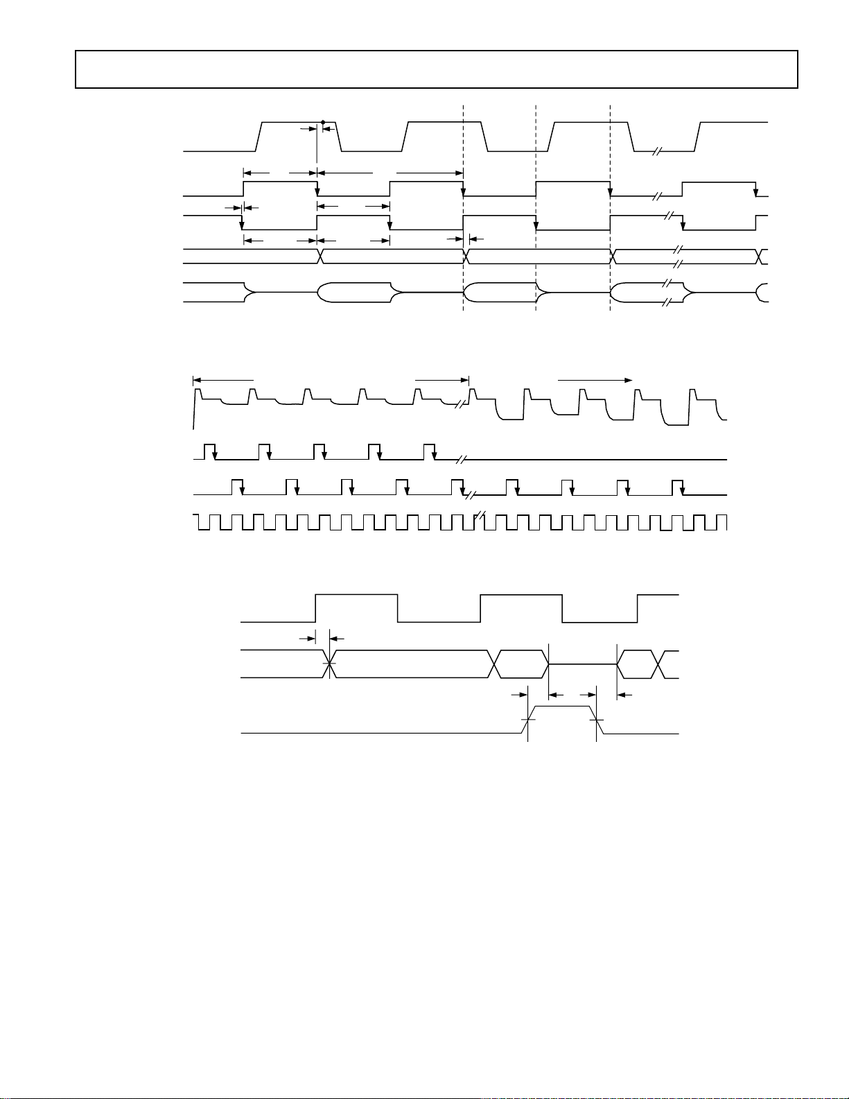
SERIAL TIMING
The 3-wire serial interface timing is shown below. To write to
the AD9816, SLOAD is first taken low. Next, a total of 16 bits
are sent to SDATA, which get latched into the AD9816 on the
rising edges of SCLK. Additional SCLK pulses will be ignored.
The first bit, R/W, should be low to specify a write operation.
The next three bits, A2–A0, are the address bits to specify the
destination register for the data word D7–D0. After all 16 bits
have been clocked, SLOAD is taken high, which internally
latches the data to the appropriate register. The read operation
also starts by taking SLOAD low. First, a one is written to R/W,
to specify a read operation. Next, the three Address Bits A2–A0
are written to specify the register that will be read. On the 8th
SCLK falling edge, SDATA will begin to output the informa-
Table IV. Offset Adjustment
tion from the desired register. After all eight data bits have been
read, SLOAD is taken back high.
Offset Register Offset Voltage
0111 1111 (LSB) +100 mV
SDATA
..
..
..
SCLK
0000 0001 +0.8 mV
0000 0000 0.0 mV
1000 0000 0.0 mV
SLOAD
1000 0001 –0.8 mV
..
..
..
SDATA
1111 1111 –100 mV
The PGA is used for correcting color imbalance and for fine
SCLK
adjustment of the input span before the ADC. Gain is variable
from 1× to 6× (0 dB to 15.5 dB) with 8-bit resolution. An all
“zeros” word (00 . . . 0) corresponds to the minimum gain, and
SLOAD
an all “ones” word (11 . . . 1) corresponds to the maximum
PGA Gain = 1 + (Gain Code/51.2)
7 6 5 4 3 2 1 0
D0 (LSB)
D1
D2
D3
D4
D5
D6
D7 (MSB)
Figure 10. PGA Registers for Red, Green and Blue
Channels
R/Wb
A2 A1 A0 D7 D6 D5 D4 D3 D2 D1
t
DH
t
LS
t
DS
t
LH
Figure 11. Write Operation Timing
R/Wb
A2 A1 A0 D7 D6 D5 D4 D3 D2 D1
t
DH
t
LS
t
DS
t
RDV
t
LH
Figure 12. Read Operation Timing
D0
D0
–10–
REV. A
Page 11

AD9816
CIRCUIT DESCRIPTIONS
Analog Input Configuration for CDS and SHA Mode
CDS Mode Operation
Figure 13 shows the equivalent input circuit for the CDS mode
of operation. The CCD signal is connected to the AD9816’s
analog inputs through a coupling capacitor C
. The CCD
IN
reference level is clamped during the CDSCLK1 pulse, when
the clamp switch closes and connects the externally-generated
3 V bias to the analog input. After the clamp switch opens
(CDSCLK1 low), the CCD data level will be level shifted by
the voltage held across C
, and the SHA will sample the input
IN
signal when the CDSCLK2 pulse goes low (see Figures 1 and 3
for CDS mode timing). In this sampling technique, the CDS
function is effectively performed across the input capacitor, C
.
IN
This CDS method has two additional considerations. First, the
CCD signal cannot be dc-coupled into the AD9816, because
the input capacitor is required. Second, the input clamp of the
AD9816 is operating as a pixel clamp, and must be asserted on
every pixel for true CDS operation. If line clamp operation is
desired, CDSCLK1 may be used at the start of each line to set
the proper dc voltage on C
. Then, during the effective pixels
IN
of each line, CDSCLK1 can be held low while CDSCLK2
samples the data levels of each pixel. Figure 5 shows the timing
for line clamp operation.
AD9816
C
CCD SIGNAL
0.1mF
1mF
IN
R
S
+5V
1.0kV
1.5kV
11
16
VING
C
OFFSET
I
BIAS
STRAY
SHA
BUFFER
CLAMP
SWITCH
3V
of the AD9816 can also handle an input signal down to
AVSS – 0.3 V without any saturation recovery issues. Although
an input level below zero volts will be clipped to the ADC’s fullscale output code, the input stage can respond quickly enough
to accurately process the next pixel that falls into the linear
input range. Any signals below AVSS – 0.3 V will turn on the
input protection diodes, and recovery from the saturated condition may take up to several milliseconds.
Input Capacitor C
IN
The recommended value for CIN is 1200 pF. This value has
been selected to provide the best overall performance when
considering three factors: input attenuation, linearity and signal
droop. The value of C
may be optimized for a particular ap-
IN
plication if these three factors are understood.
1. Attenuation (Gain Error)
The input voltage will be attenuated by the interaction of
C
and C
IN
an attenuation of about 0.8% when C
error will increase accordingly as the value of C
STRAY
. C
is less than 10 pF, which results in
STRAY
is 1200 pF. The gain
IN
is decreased.
IN
2. Linearity
The input capacitance of the AD9816 is shown in Figure 8
as C
. A small portion of this capacitance is junction
STRAY
capacitance, which will vary nonlinearly as the input voltage
to the AD9816 changes. When the input voltage is attenuated by the combination of C
IN
and C
, there will be a
STRAY
small nonlinear component caused by the input junction
capacitance. The magnitude of the junction capacitance will
cause a 1 LSB (0.024%) nonlinearity over the 3 V input
range when a 1200 pF C
increase if a smaller C
is used. This nonlinearity will
IN
is used.
IN
3. Droop
The input bias current of the AD9816 is typically 10 nA and
is constant regardless of the AD9816’s input voltage. The
droop of the voltage across C
can be calculated with the
IN
following equation:
17 18
CDSCLK1 CDSCLK2
Figure 13. CDS Mode Input Circuit (All Channels Identical)
Input Signal Range for CDS Mode
An input dc bias level of 3 V allows a maximum 3 V p-p signal
swing from the CCD. Figure 14 shows a typical full-scale input
waveform to the AD9816, illustrating the allowable input range.
With a reference level of 3 V, the AD9816 can tolerate up to
2 V of reset feedthrough above the reference level. The inputs
Figure 14. CCD Input Signal Clamped to 3 V
–11–REV. A
i
BIAS
dV =
×(t)
C
IN
where t is the time between clamp intervals. Between the
adjacent pixels of a scanned line, this droop will be insignificant. Between scanned lines, a 1 ms delay will produce a
droop of about 10 mV, which can be easily clamped on the
first pixel of the next line. If the value of C
is reduced, the
IN
droop will increase accordingly.
5V MAX RESET FEEDTHROUGH
3V REFERENCE LEVEL
(SET BY INPUT CLAMP)
MAX PEAK-PEAK SIGNAL
0V MAX DATA LEVEL
–0.3V MAX SATURATED DATA LEVEL
Page 12

AD9816
Line Clamp
If a line clamp technique is implemented (see Figure 5 for
timing), the value of C
should be increased to more than
IN
1200 pF. The main requirement for line clamp is to keep the
signal droop below 1 LSB across a scanned line. For example, if
a CCD with 5400 effective pixels is clocked at 2 MHz, then
t = 2.7 ms. One LSB at 12 bits with a 3 V full scale is 732 µV.
Rearranging the above droop equation:
i
MIN
BIAS
=
×t
dV
In this case, C
C
= 37 nF, and a convenient standard value of
MIN
0.047 µF will be adequate.
SHA Mode Operation
When the AD9816 is configured for SHA mode operation, the
OFFSET pin functions as an offset adjustment input. Figure
15 shows a simplified diagram of the AD9816’s inputs when SHA
mode is selected. A positive dc voltage may be applied to OFFSET
which will be subtracted from all three input channels in the
input stage of the AD9816. The maximum input voltage to the
analog input pins or the OFFSET pin in SHA mode is 3 V.
The OFFSET feature is provided to allow coarse offset adjustment of the input signal. If the signal is sampled with respect to
ground, any positive offset on the input signal will subtract from
the dynamic range of the ADC. For example, an input signal
that spans from 1.5 V to 2.5 V cannot utilize all of the available
dynamic range, using either the 1.5 V or 3 V span. However, by
applying a dc value of 1.5 V to the OFFSET pin, the input
signal will be level-shifted down to 0 V to 1 V. This would
allow the use of the 3 V span and a PGA gain of three to use
the entire ADC dynamic range.
If no dc offset adjustment is desired, the OFFSET pin should
be grounded. The input signal will be sampled with respect to
ground.
AD9816
VINR
VING
VINB
OFFSET
BUFFER
BUFFER
BUFFER
12kV
CDSCLK1
SHA
SHA
SHA
CDSCLK2
Figure 15. SHA Mode Input Circuit
Programmable Gain Amplifiers
The AD9816 has three programmable amplifiers, one for each
channel. The gain is variable from 1 V/V (0 dB) to 5.98 V/V
(15.5 dB) in 256 increments. Figure 16 shows the PGA gain
transfer function. The gain of the PGA can be calculated according to the equation:
PGA Gain =1+
6
5
4
3
PGA GAIN – V/V
2
1
051 255102 153 204
GAIN REGISTER CODE – Decimal
Gain Code
51.2
Figure 16. PGA Gain Transfer Function
The analog outputs of the three PGAs are multiplexed to the input
of the 12-bit ADC. The differential output of the MUX is also
buffered and externally available at Pins 43 and 44 (PGAOUT_C
and PGAOUT_T, respectively). The timing diagrams, Figures 1 through 4, show the timing relationships between the
analog inputs, CDSCLK2, ADCCLK, and PGAOUT_T and
PGAOUT_C. The CDSCLK2 pulse resets the outputs of all
three PGAs to an internal bias level. The first rising edge of
ADCCLK after the rising edge of CDSCLK2 will switch the
MUX to the red PGA output. The second ADCCLK rising
edge switches the MUX to the green PGA output, and the third
rising edge switches the MUX to the blue PGA output.
PGA Outputs
The PGAOUT_T and PGAOUT_C signals represent the differential input to the ADC, and are complementary. Both signals
will reset to 3.5 V while CDSCLK2 is high. The voltage swing
of each output is equal to one-half of the ADC’s full-scale voltage, centered at 3.5 V. Table V shows the relationship between
the analog input voltage, the PGA output voltage and the ADC
input voltage.
Figure 18 shows the PGA output voltages for three different
color pixel amplitudes. In this example, the red pixel has the
largest amplitude, and the blue pixel has the smallest amplitude.
Because the PGAOUT_T and PGAOUT_C outputs are internally buffered by source followers, they are not an exact representation of the differential ADC input signal. PGAOUT_T and
PGAOUT_C should only be used during evaluation; performance of the AD9816 is only guaranteed with these two pins
unconnected.
–12–
REV. A
Page 13

AD9816
PGAOUT_T PGAOUT_C
RED
PGA
GREEN
BLUE
PGA
PGA
3:1
DIFF
MUX
SELECT
2
MUX
CONTROL
12-BIT ADC
ADCCLK
CDSCLK2
Figure 17. PGA/MUX Circuit Configuration
PIXEL n
ANALOG
INPUTS
CDSCLK2
ADCCLK
PGAOUT_T
PGAOUT_C
GREEN(n–1)
BLUE
GREEN
RED
BLUE(n–1)
RESET
RED(n)
GREEN(n)
BLUE(n)
RESET
4.25V
3.5V
2.75V
Figure 18. PGA Output Voltages (ADC Input Range = 3 V)
Table V. Voltage Swing of PGA Outputs
Analog Differential
Input ADC
Voltage
0.00
1.50
3.00
0.00
0.75
1.50
NOTES
1
2
3
1
PGAOUT_T PGAOUT_C Input
2
2
2
3
3
3
2.75 4.25 1.5
3.50 3.50 0.0
4.25 2.75 +1.5
3.125 3.875 0.75
3.50 3.50 0.0
3.875 3.125 +0.75
Analog input voltage in CDS mode is the difference between the CCD’s reference and data levels.
3.0 V Input Range.
1.5 V Input Range.
Analog-to-Digital Converter
The AD9816 uses a high speed 12-bit ADC core. This CMOS
converter is designed to run at 6 MSPS with good linearity and
noise performance. Figure 19 shows the INL and DNL performance of a typical AD9816 device, running at 6 MHz in 3-channel
CDS mode using the timing shown in Figure 1. The following
timing parameters were used: t
t
= 20 ns, t
C1
and t
C2C1
= 170 ns, tC1 = 80 ns, t
C1C2
= 230 ns.
CRA
= 500 ns, t
= 3 ns, t
ADC2
ADCLK
= 83 ns,
= 83 ns,
C2AD
The digital outputs of the AD9816 follow a straight binary
coding scheme. Table VI shows the digital output coding for
the 3 V input span.
0.2
INL
DNL
–0.2
–0.4
–0.6
–0.8
–1.2
–1.4
–1.6
–0.5
–1.0
0.0
0
1.5
1.0
0.5
0.0
0
1200400 1600800
1200400 1600800 2000 2400 2800 3200 3600
2000 2400 2800 3200 3600
MAX INL 0.18
MIN INL –1.46
MAX DNL 0.31
MIN DNL –0.33
4095
4095
Figure 19. Typical Linearity Performance
Table VI. Digital Output Format
Input Voltage
1
Digital Outputs
3.0 – 1 LSB 1111 1111 1111
3.0 – 2 LSB 1111 1111 1110
0.0 + 1 LSB 0000 0000 0001
0.0 0000 0000 0000
NOTE
1
Analog input voltage in CDS mode is the difference between the
CCD’s reference and data levels.
–13–REV. A
Page 14

AD9816
APPLICATIONS INFORMATION
CDS Mode Circuit
The recommended circuit configuration for CDS mode operation is shown in Figure 20. The input coupling capacitor value
of 1200 pF is recommended, but this value may be adjusted to
suit a particular application (see Circuit Descriptions). A single
ground plane is recommended for the AD9816. A separate power
supply may be used for DRVDD, the digital driver supply, but this
V
DD
AVDD
AVSS
CAPT
CAPT
CAPB
CAPB
VREF
CML
VINR
AVSS
VING
0.1mF1.0mF
444342
PGAOUT_T
PGAOUT_C
AVSS
VINB
121314
0.01mF
10mF
0.01mF0.1mF
0.1mF
+
10mF 0.1mF
0.1mF
+
0.1mF
1.0mF
RED_IN
GREEN_IN
BLUE_IN
1200pF
1200pF
1200pF
1
2
3
4
5
6
7
8
9
10
11
V
DD
0.1mF
supply pin should still be decoupled to the same ground plane
as the rest of the AD9816. The loading of the digital outputs
should be minimized, either by using short traces to the digital
ASIC, or by using external digital buffers. All 0.01 µF and
0.1 µF decoupling capacitors should be located as close as pos-
sible to the AD9816 pins. Also, the 1200 pF input capacitors
should be located close the AD9816’s analog input pins.
NC
AVSS
1.5kV
OEB
DB10
DB11(MSB)
41
403938
OEB
DB10
DB11 (MSB)
AD9816
AVDD
OFFSET
CDSCLK1
15
161718
1kV
DB9
DB8
DB7
373635
DB9
DB8
DB7
CDSCLK2
ADCCLK
DVSS
202122
19
V
DD
DB6
34
DB6
DRVDD
DRVSS
DB5
DB4
DB3
DB2
DB1
DB0 (LSB)
DVSS
SLOAD
SDATA
SCLK
DVDD
NC
NC = NO CONNECT
ADCCLK
CDSCLK2
CDSCLK1
33
32
31
30
29
28
27
26
25
24
23
V
0.1mF0.01mF
0.01mF
DB5
DB4
DB3
DB2
DB1
DB0 (LSB)
DD
V
DD
0.1mF
SLOAD
SDATA
SCLK
Figure 20. Recommended Circuit for CDS Mode
–14–
REV. A
Page 15

AD9816
SHA Mode Circuit
The circuit configuration for SHA mode is identical to CDS
mode except for two differences: the analog inputs should be
dc-coupled, and the OFFSET pin is tied to ground or a desired
dc voltage (see Circuit Descriptions). In CIS applications, the
V
DD
AVDD
AVSS
CAPT
CAPT
CAPB
CAPB
VREF
CML
VINR
AVSS
VING
444342
PGAOUT_T
AVSS
121314
0.01mF0.1mF
10mF
1.0mF
0.01mF
1
2
+
V
0.1mF1.0mF
3
4
5
6
7
8
9
10
11
V
DD
DD
R1
OPTIONAL DC OFFSET
R2
0.1mF
0.1mF
10mF 0.1mF
0.1mF
+
0.1mF
RED_IN
GREEN_IN
BLUE_IN
reference black level of the CIS can be connected to the OFFSET pin, to remove the dc offset. Removing the coarse offset of
the CIS signal will allow the dynamic range of the AD9816 to
be maximized.
OEB
DB10
DB9
DB8
DB7
41
NC
OEB
PGAOUT_C
AD9816
VINB
AVSS
AVDD
15
DB11(MSB)
403938
DB10
DB11 (MSB)
OFFSET
CDSCLK1
161718
GROUND-REFERENCED SAMPLING
373635
DB9
DB8
DB7
CDSCLK2
ADCCLK
DVSS
202122
19
DB6
34
DB6
DRVDD
DRVSS
DB5
DB4
DB3
DB2
DB1
DB0 (LSB)
DVSS
SLOAD
SDATA
SCLK
DVDD
NC
NC = NO CONNECT
0.01mF
ADCCLK
CDSCLK2
CDSCLK1
0.01mF 0.1mF
33
32
DB5
31
DB4
30
DB3
29
DB2
28
DB1
27
DB0 (LSB)
26
25
24
23
V
DD
0.1mF
V
DD
SLOAD
SDATA
SCLK
Figure 21. Recommended Circuit for SHA Mode
–15–REV. A
Page 16

AD9816
0.041 (1.03)
0.029 (0.73)
SEATING
PLANE
OUTLINE DIMENSIONS
Dimensions shown in inches and (mm).
44-Lead MQFP
(S-44)
0.529 (13.45)
44
0.510 (12.95)
0.398 (10.1)
0.390(9.90)
TOP VIEW
(PINS DOWN)
34
0.096 (2.45)
MAX
1
33
0.333 (8.45)
0.327 (8.3)
C3324a–0–10/98
0.01 (0.25) MIN
0.009 (0.23)
0.005 (0.13)
0.083 (2.1)
0.077 (1.95)
11
12
0.031 (0.80)
BSC
23
22
0.018 (0.45)
0.012 (0.30)
–16–
PRINTED IN U.S.A.
REV. A
 Loading...