

Page 1
Complete 10-Bit 18 MSPS
a
FEATURES
18 MSPS Correlated Double Sampler (CDS)
6 dB to 40 dB 10-Bit Variable Gain Amplifier (VGA)
Low Noise Clamp Circuits
Preblanking Function
10-Bit 18 MSPS A/D Converter
3-Wire Serial Digital Interface
3 V Single Supply Operation
Low Power CMOS
48-Lead LQFP Package
APPLICATIONS
PC Cameras
Digital Still Cameras
PRODUCT DESCRIPTION
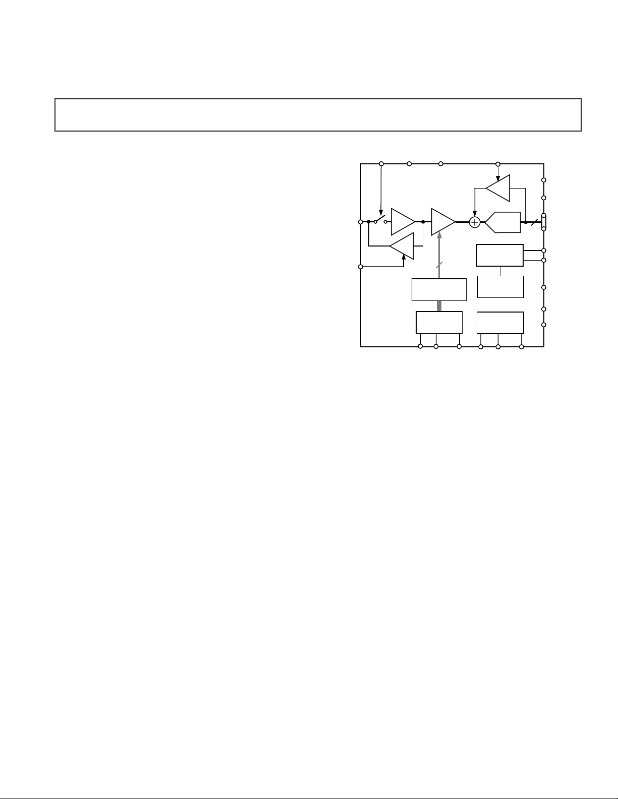
The AD9804 is a complete analog signal processor for CCD
applications. It features an 18 MHz single-channel architecture
designed to sample and condition the outputs of interlaced and
progressive scan area CCD arrays. The AD9804’s signal chain
consists of an input clamp, correlated double sampler (CDS),
digitally controlled VGA, black level clamp, and a 10-bit A/D
converter. The internal VGA gain register is programmed through
a 3-wire serial digital interface.
CCDIN
CLPDM
CCD Signal Processor
AD9804
FUNCTIONAL BLOCK DIAGRAM
PBLK
AVDD
CDS
CLP
AD9804
AVSS
6dB TO 40dB
VGA
VGA GAIN
REGISTER
DIGITAL
INTERFACE
SL
CLPOB
CLP
10-BIT
ADC
BANDGAP
10
SDATASCK
REFERENCE
INTERNAL
BIAS
INTERNAL
TIMING
DATACLKSHDSHP
DRVDD
DRVSS
10
DOUT
VR
T
VRB
CML
DVDD
DVSS
REV. 0
Information furnished by Analog Devices is believed to be accurate and
reliable. However, no responsibility is assumed by Analog Devices for its
use, nor for any infringements of patents or other rights of third parties
which may result from its use. No license is granted by implication or
otherwise under any patent or patent rights of Analog Devices.
One Technology Way, P.O. Box 9106, Norwood, MA 02062-9106, U.S.A.
Tel: 781/329-4700 www.analog.com
Fax: 781/326-8703 © Analog Devices, Inc., 2000
Page 2
AD9804–SPECIFICATIONS
(T
to T
ANALOG SPECIFICATIONS
MIN
, AVDD = DVDD = 3.0 V, f
MAX
Parameter Min Typ Max Unit
TEMPERATURE RANGE
Operating –20 +85 °C
Storage –65 +150 °C
POWER SUPPLY VOLTAGE
Analog, Digital, Digital Driver 2.8 3.0 3.6 V
POWER CONSUMPTION 85 mW
MAXIMUM CLOCK RATE 18 MHz
CORRELATED DOUBLE SAMPLER (CDS)
Allowable CCD Reset Transient
Max Input Range before Saturation
Max CCD Black Pixel Amplitude
1
1
1
VARIABLE GAIN AMPLIFIER (VGA)
Gain Control Resolution 1024 Steps
Gain Range (VGA Gain Curve Shown in Figure 5)
Min Gain (Code 95) 468dB
Max Gain (Code 1023) 38 40 42 dB
BLACK LEVEL CLAMP
Clamp Level (At ADC Output) 32 LSB
A/D CONVERTER
Resolution 10 Bits
No Missing Codes 10 Bits Guaranteed
Full-Scale Input Voltage 2.0 V
VOLTAGE REFERENCE
Reference Top Voltage (VRT) 2.0 V
Reference Bottom Voltage (VRB) 1.0 V
NOTES
1
Input signal characteristics defined as follows:
DATACLK
= f
= f
SHP
= 18 MHz, unless otherwise noted.)
SHD
500 mV
1.0 V p-p
100 mV
500mV TYP
RESET
TRANSIENT
Specifications subject to change without notice.
100mV MAX
OPTICAL
BLACK PIXEL
DIGITAL SPECIFICATIONS
1V MAX
INPUT
SIGNAL RANGE
(DRVDD = 2.7 V, CL = 20 pF.)
Parameter Symbol Min Typ Max Unit
LOGIC INPUTS
High Level Input Voltage V
Low Level Input Voltage V
High Level Input Current I
Low Level Input Current I
Input Capacitance C
IH
IL
IH
IL
IN
2.1 V
0.6 V
10 µA
10 µA
10 pF
LOGIC OUTPUTS
High Level Output Voltage V
Low Level Output Voltage V
High Level Output Current I
Low Level Output Current I
Specifications subject to change without notice.
OH
OL
OH
OL
2.1 V
0.6 V
50 µA
50 µA
–2–
REV. 0
Page 3
AD9804
WARNING!
ESD SENSITIVE DEVICE
TIMING SPECIFICATIONS
(CL = 20 pF, f
= 18 MHz, timing shown in Figures 1 and 2.)
CLK
Parameter Symbol Min Typ Max Unit
SAMPLE CLOCKS
DATACLK, SHP, SHD Clock Period t
DATACLK Hi/Low Pulsewidth t
SHP Pulsewidth t
SHD Pulsewidth t
CLPDM Pulsewidth t
CLPOB Pulsewidth
1
SHP Rising Edge to SHD Falling Edge t
SHP Rising Edge to SHD Rising Edge t
Internal Clock Delay t
Inhibited Clock Period t
CONV
ADC
SHP
SHD
CDM
t
COB
S1
S2
ID
INH
20 27.7 ns
10 14 ns
10 14 ns
410 Pixels
210 Pixels
20 27 ns
20 27 ns
10 ns
55.6 ns
3.0 ns
DATA OUTPUTS
Output Delay t
Output Hold Time t
OD
H
6.0 7.6 ns
14.5 16 ns
Pipeline Delay 9 Cycles
SERIAL INTERFACE
Maximum SCK Frequency f
SL to SCK Setup Time t
SCK to SL Hold Time t
SDATA Valid to SCK Rising Edge Setup t
SCK Falling Edge to SDATA Valid Hold t
SCK Falling Edge to SDATA Valid Read t
NOTES
1
Minimum CLPOB pulsewidth is for functional operation only. Wider typical pulses are recommended to achieve low noise clamp performance.
Specifications subject to change without notice
SCLK
LS
LH
DS
DH
DV
10 MHz
10 ns
10 ns
10 ns
10 ns
10 ns
ABSOLUTE MAXIMUM RATINGS
With
Respect
Parameter To Min Max Unit
Model Range Description Option
AD9804JST –20°C to +85°CThin Plastic ST-48
ORDERING GUIDE
Temperature Package Package
AVDD AVSS –0.3 +3.9 V
DVDD DVSS –0.3 +3.9 V
DRVDD DRVSS –0.3 +3.9 V
Digital Outputs DRVSS –0.3 DRVDD + 0.3 V
SHP, SHD, DATACLK DVSS –0.3 DVDD + 0.3 V
CLPOB, CLPDM, PBLK DVSS –0.3 DVDD + 0.3 V
SCK, SL, SDATA DVSS –0.3 DVDD + 0.3 V
VRT, VRB, CMLEVEL AVSS –0.3 AVDD + 0.3 V
THERMAL CHARACTERISTICS
Thermal Resistance
48-Lead LQFP Package
θ
= 92°C/W
JA
BYP1–4, CCDIN AVSS –0.3 AVDD + 0.3 V
Junction Temperature 150 °C
Lead Temperature 300 °C
(10 sec)
CAUTION
ESD (electrostatic discharge) sensitive device. Electrostatic charges as high as 4000 V readily
accumulate on the human body and test equipment and can discharge without detection. Although
the AD9804 features proprietary ESD protection circuitry, permanent damage may occur on
devices subjected to high-energy electrostatic discharges. Therefore, proper ESD precautions are
recommended to avoid performance degradation or loss of functionality.
Quad Flatpack
(LQFP)
REV. 0
–3–
Page 4

AD9804
NC
NC
(LSB) D0
D1
D2
D3
D4
D5
D6
D7
D8
(MSB) D9
NC = NO CONNECT
PIN FUNCTION DESCRIPTIONS
PIN CONFIGURATION
SCK
SDATASLNC
DVSS
RSTB
DVSS
AD9804
TOP VIEW
NC
DVDD
PBLK
DVSS
CLPOB
48 47 46 45 44 39 3843 42 41 40 37
1
PIN 1
IDENTIFIER
2
3
4
5
6
7
8
9
10
11
12
13 14 15 16 17 18 19 20 21 22 23 24
DRVSS
DRVDD
(Not to Scale)
DVSS
DATACLK
DVDD
SHP
VRB
SHD
VRT
CML
NC
CLPDM
36
35
34
33
32
31
30
29
28
27
26
25
NC
AVSS
NC
AVDD
BYP4
NC
CCDIN
BYP2
BYP1
AVDD
AVSS
AVSS
Pin No. Mnemonic Type Description
1, 2, 18, 24, 31 NC NC Internally Not Connected
34, 36, 45
3–12 D0–D9 DO Digital Data Outputs
13 DRVDD P Digital Output Driver Supply
14 DRVSS P Digital Output Driver Ground
15, 41, 42, 44 DVSS P Digital Ground
16 DATACLK DI Digital Data Output Latch Clock
17, 40 DVDD P Digital Supply
19 PBLK DI Preblanking Clock Input
20 CLPOB DI Black Level Clamp Clock Input
21 SHP DI CDS Sampling Clock for CCD’s Reference Level
22 SHD DI CDS Sampling Clock for CCD’s Data Level
23 CLPDM DI Input Clamp Clock Input
25, 26, 35 AVSS P Analog Ground
27, 33 AVDD P Analog Supply
28 BYP1 AO Internal Bias Level Decoupling
29 BYP2 AO Internal Bias Level Decoupling
30 CCDIN AI Analog Input for CCD Signal
32 BYP4 AO Internal Bias Level Decoupling
37 CML AO Internal Bias Level Decoupling
38 VRT AO A/D Converter Top Reference Voltage Decoupling
39 VRB AO A/D Converter Bottom Reference Voltage Decoupling
43 RSTB DI Chip Reset Control. Active Low
46 SL DI Serial Digital Interface Load Pulse.
47 SDATA DI Serial Digital Interface Data
48 SCK DI Serial Digital Interface Clock
TYPE: AI = Analog Input, AO = Analog Output, DI = Digital Input, DO = Digital Output, P = Power.
–4–
REV. 0
Page 5

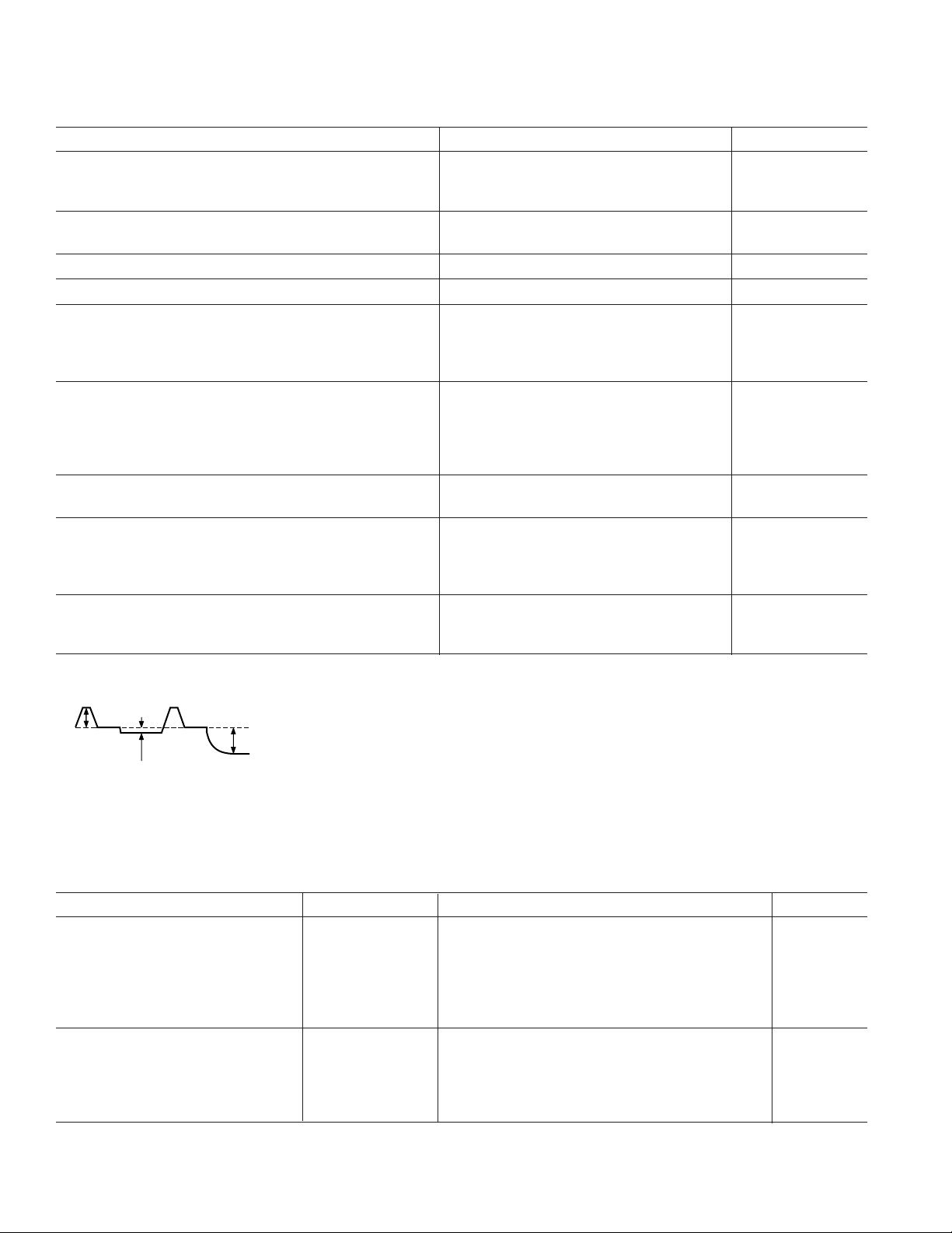
TIMING DIAGRAMS
N–10 N–9 N–8 N–1 N
N N+1 N+2 N+9 N+10
t
ID
t
ID
t
S1
t
S2
t
CP
t
INH
t
OD
t
H
NOTES:
1. RECOMMENDED PLACEMENT FOR DATACLK RISING EDGE IS BETWEEN THE SHD RISING EDGE AND NEXT SHP FALLING EDGE.
2. CCD SIGNAL IS SAMPLED AT SHP AND SHD RISING EDGES.
SHP
SHD
DATACLK
OUTPUT
DATA
CCD
SIGNAL
CCD
SIGNAL
EFFECTIVE PIXELS
CLPOB
CLPDM
OPTICAL BLACK PIXELS
HORIZONTAL
BLANKING
DUMMY PIXELS EFFECTIVE PIXELS
PBLK
NOTES:
1. CLPOB AND CLPDM WILL OVERWRITE PBLK. PBLK WILL NOT AFFECT CLAMP OPERATION IF OVERLAPPING CLPDM AND/OR CLPOB.
2. PBLK SIGNAL IS OPTIONAL.
3. DIGITAL OUTPUT DATA WILL BE ALL ZEROS DURING PBLK. OUTPUT DATA LATENCY IS 9 DATACLK CYCLES.
OUTPUT
DATA
EFFECTIVE PIXEL DATA
OB PIXEL DATA DUMMY BLACK EFFECTIVE DATA
AD9804
Figure 1. Pixel Rate Timing
Figure 2. Typical Line Clamp Timing
REV. 0
–5–
Page 6

AD9804
,
PROGRAMMING THE SERIAL INTERFACE
Table I. VGA Gain Register Contents (Default Value x096)
MSB LSB
D9 D8 D7 D6 D5 D4 D3 D2 D1 D0 Gain (dB)
00010111116.0
••
••
••
111111111039.965
111111111140.0
RNW ADDRESS BITS
SDATA
SCK
SL
0
t
DS
NOTES:
1. SDATA BITS ARE INTERNALLY LATCHED ON THE RISING EDGES OF SCK.
2. RNW = READ, NOT WRITE. SET LOW FOR WRITE OPERATION.
3. INTERNAL VGA GAIN REGISTER UPDATE OCCURS AT SL RISING EDGE.
t
DH
t
LS
0010 D0D1 D2 D3 D4 D5 D6 D7 D8 D9 D10
DATA BITS
Figure 3. Serial Write Operation
RNW
ADDRESS BITS
SDATA
SCK
SL
1D0D1D2D3D4D5D6D7D8D9D10
t
DS
NOTES:
1. RNW = READ, NOT WRITE. SET HIGH FOR READ OPERATION.
2. THE RNW BIT AND THE FOUR ADDRESS BITS MUST BE WRITTEN TO THE AD9804. SDATA IS LATCHED ON SCK RISING EDGES.
3. SERIAL DATA FROM VGA GAIN REGISTER IS VALID STARTING AFTER THE 5TH SCK FALLING EDGE
t
DH
t
LS
0010
DATA BITS
t
DV
AND IS UPDATED ON SCK FALLING EDGES.
Figure 4. Serial Readback Operation
t
LH
t
LH
–6–
REV. 0
Page 7

AD9804
VARIABLE GAIN AMPLIFIER (VGA) OPERATION
DETAILS
The VGA stage provides a gain range of 6 dB to 40 dB, programmable with 10-bit resolution through the serial digital
interface. The minimum gain of 6 dB is needed to match a 1 V
input signal with the ADC full-scale range of 2 V. When compared to 1 V full-scale systems (such as ADI’s AD9803), the
equivalent gain range is 0 dB to 34 dB.
The VGA gain curve is divided into two separate regions. When
the VGA Gain Register code is between 0 and 511, the curve
follows a (1 + x)/(1 – x) shape, which is similar to a “linear-indB” characteristic. From code 512 to code 1023, the curve follows
a “linear-in-dB” shape. The exact VGA gain can be calculated
for any Gain Register value by using the following two equations:
Code Range Gain Equation (dB)
0–511 Gain = 20 log
([658 + code]/[658 – code]) + 3.6
10
512–1023 Gain = (0.0354)(code) + 3.6
As shown in the Analog Specifications, only the VGA gain range
from 2 dB to 36 dB has been specified. This corresponds to a
VGA gain code range of 95 to 1023.
40
34
28
22
VGA GAIN – dB
16
10
4
127 255 383 511 639 767 895 1023
0
VGA GAIN REGISTER CODE
Figure 5. VGA Gain Curve
APPLICATIONS INFORMATION
The AD9804 is a complete Analog Front-End (AFE) product
for PC camera, digital still camera, and camcorder applications.
As shown in Figure 6, the CCD image (pixel) data is buffered
and sent to the AD9804 analog input through a series input
capacitor. The AD9804 performs the dc restoration, CDS, gain
adjustment, black level correction, and analog-to-digital conversion. The AD9804’s digital output data is then processed by the
image processing ASIC. The internal registers of the AD9804
used to control gain, offset level, and other functions are programmed by the ASIC or microprocessor through a 3-wire serial
digital interface. A system timing generator provides the clock
signals for both the CCD and the AFE.
Generating the Reset (RSTB) Signal
After power-on, the AD9804 must be reset using Pin 43 (RSTB).
The reset pulse must be an active low signal, which goes low for
at least 100 ns after the power supplies have settled. After the
RSTB signal returns high, the AD9804 is internally reset to the
default VGA gain register value. If a system reset pulse is not
available, a simple RC network may be used, as shown in Figure
7. The time constant of this network should be comparable
to the power-on time of the AD9804’s power supplies. For
example, if the power supplies have a power-on time of 10 ms,
the RC network should have a time constant of 10 ms, giving
R = 10 kΩ and C = 1.0 µF.
Serial writes to the AD9804 internal registers must not be performed until 20 µs after the reset pulse has occurred. This allows
enough time for internal calibration routines to be completed.
SDATA and SCK may be active before the reset sequence, but
SL should be held logic HIGH until 20 µs or more after the reset.
Alternatively, placing series resistors close to the digital output pins may help reduce noise.
Grounding and Decoupling Recommendations
As shown in Figure 7, a single ground plane is recommended for
the AD9804. This ground plane should be as continuous as
possible, particularly around Pins 25 through 39. This will ensure
that all analog decoupling capacitors provide the lowest possible
impedance path between the power and bypass pins and their
respective ground pins. All decoupling capacitors should be
located as close as possible to the package pins. A single clean
power supply is recommended for the AD9804, but a separate
digital driver supply may be used for DRVDD (Pin 13). DRVDD
should always be decoupled to DRVSS (Pin 14), which should
be connected to the analog ground plane. Advantages of using a
separate digital driver supply include using a lower voltage (2.7 V)
to match levels with a 2.7 V ASIC, reducing digital power dissipation, and reducing potential noise coupling. If the digital outputs
(Pins 3–12) must drive a load larger than 20 pF, buffering is
recommended to reduce digital code transition noise.
REV. 0
CCD
V-DRIVE
OUT
DIGITAL
OUTPUTS
SERIAL
INTERFACE
DIGITAL IMAGE
PROCESSING
ASIC
V
OUT
BUFFER
0.1F
CCD
TIMING
AD9804
CCDIN
GENERATOR
VGA GAIN
CDS/CLAMP
TIMING
TIMING
ADC
Figure 6. System Block Diagram
–7–
Page 8

AD9804
DATA
OUTPUTS
10
SERIAL
INTERFACE
(LSB) D0
(MSB) D9
3V
DRIVER
SUPPLY
1.0F
3
SCK
SDATASLNC
DVSS
RSTB
NC
1
NC
PIN 1
2
IDENTIFIER
3
D1
4
D2
5
D3
6
D4
7
D5
8
D6
9
D7
10
D8
11
12
13 14 15 16 17 18 19 20 21 22 23 24
DRVDD
0.1F
DVSS
DRVSS
AD9804
TOP VIEW
(Not to Scale)
NC
DVDD
DATACLK
3V
ANALOG SUPPLY
10k⍀
DVSS
DVSS
VRB
DVDD
SHP
SHD
PBLK
CLPOB
0.1F
1.0F
1.0F
0.1F
VRT
CML
3748 47 46 45 44 39 3843 42 41 40
36
35
34
33
32
31
30
29
28
27
26
25
NC
NC = NO CONNECT
CLPDM
6
NC
AVSS
NC
AVDD
BYP4
NC
CCDIN
BYP2
BYP1
AVDD
AVSS
AVSS
CLOCK
INPUTS
0.1F
0.1F
0.1F
0.1F
0.1F
0.1F
3V
ANALOG
SUPPLY
CCD
SIGNAL
3V
ANALOG
SUPPLY
C01633–0–10/00 (rev. 0)
0.1F
3V
ANALOG SUPPLY
Figure 7. AD9804 Circuit Configuration
OUTLINE DIMENSIONS
Dimensions shown in inches and (mm).
48-Lead, LQFP
(ST-48)
0.063 (1.60)
0.030 (0.75)
0.018 (0.45)
COPLANARITY
0.003 (0.08)
0.004 (0.09)
MAX
0.008 (0.2)
0.354 (9.00) BSC SQ
48
1
12
0ⴗ
13
MIN
0.019 (0.5)
7ⴗ
0ⴗ
0.006 (0.15)
0.002 (0.05)
TOP VIEW
(PINS DOWN)
BSC
0.011 (0.27)
0.006 (0.17)
SEATING
PLANE
37
24
36
25
0.276
(7.00)
BSC
SQ
0.057 (1.45)
0.053 (1.35)
–8–
REV. 0
 Loading...