

Page 1
14-Bit, 2400 MSPS RF DAC
FEATURES
DOCSIS 3.0 performance: 4 QAM carriers
ACLR over full band (47 MHz to 1 GHz)
−75 dBc @ f
−72 dBc @ f
−67 dBc @ f
Unequalized MER = 42 dB
On chip and bypassable
4 QAM encoders with SRRC filters, 16× to 512× interpolation,
rate converters, and modulators
Flexible data interface: 4, 8, 16, or 32 bits wide with parity
Power: 1.6 W (I
Direct to RF synthesis support with f
Built-in self-test (BIST) support
Input connectivity check
Internal random number generator
APPLICATIONS
Broadband communications systems
CMTS/DVB
Cellular infrastructure
Point-to-point wireless
GENERAL DESCRIPTION
The AD9789 is a flexible QAM encoder/interpolator/upconverter
combined with a high performance, 2400 MSPS, 14-bit RF digitalto-analog converter (DAC). The flexible digital interface can
accept up to four channels of complex data. The QAM encoder
supports constellation sizes of 16, 32, 64, 128, and 256 with
SRRC filter coefficients for all standards.
= 200 MHz
OUT
= 800 MHz (noise)
OUT
= 800 MHz (harmonics)
OUT
= 20 mA, f
FS
= 2.4 GHz, LVDS interface)
DAC
mix mode
S
with 4-Channel Signal Processing
AD9789
The on-chip rate converter supports a wide range of baud rates
with a fixed DAC clock. The digital upconverter can place the
channels from 0 to 0.5 × f
channels to be synthesized and placed anywhere from dc to f
The AD9789 includes a serial peripheral interface (SPI) for
device configuration and status register readback. The flexible
digital interface can be configured for data bus widths of 4, 8,
16, and 32 bits. It can accept real or complex data.
The AD9789 operates from 1.5 V, 1.8 V, and 3.3 V supplies for
a total power consumption of 1.6 W. It is supplied in a 164-ball
chip scale package ball grid array for lower thermal impedance
and reduced package parasitics. No special power sequencing
is required. The clock receiver powers up muted to prevent
start-up noise.
PRODUCT HIGHLIGHTS
1. Highly integrated and configurable QAM mappers, inter-
polators, and upconverters for direct synthesis of one to
four DOCSIS- or DVB-C-compatible channels in a block.
2. Low noise and intermodulation distortion (IMD) perfor-
mance enable high quality synthesis of signals up to 1 GHz.
3. Flexible data interface supports LVDS for improved SFDR
or CMOS input data for less demanding applications.
4. Interface is configurable from 4-bit nibbles to 32-bit words
and can run at up to 150 MHz CMOS or 150 MHz LVDS
double data rate (DDR).
5. Manufactured on a CMOS process, the AD9789 uses a
proprietary switching technique that enhances dynamic
performance.
. This permits four contiguous
DAC
DAC
/2.
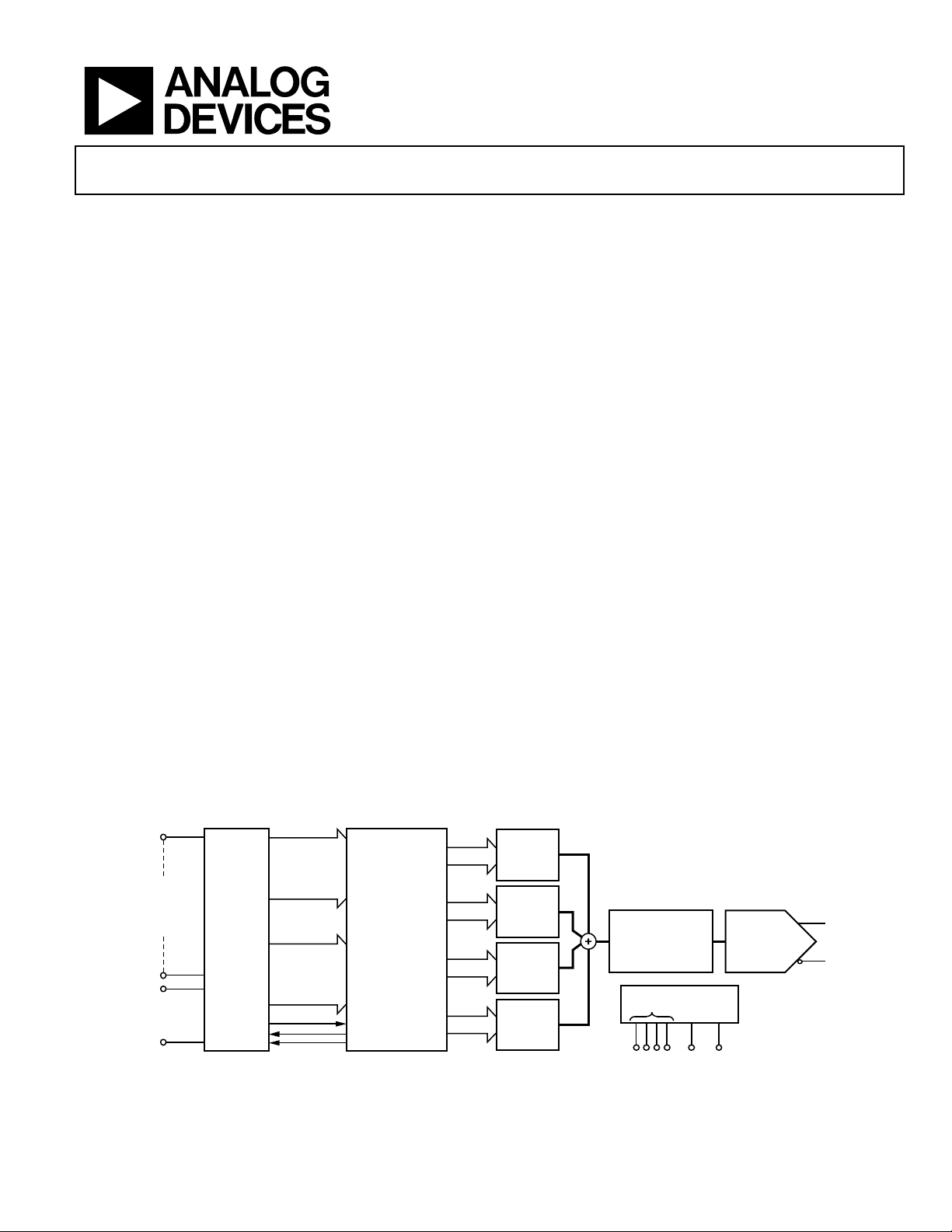
FUNCTIONAL BLOCK DIAGRAM
CMOS
0TO 15
32 INPUT
PINS
AND
2PARITY
PINS
DCO
FS
Rev. A
Information furnished by Analog Devices is believed to be accurate and reliable. However, no
responsibility is assumed by Analog Devices for its use, nor for any infringements of patents or other
rights of third parties that may result from its use. Specifications subject to change without notice. No
license is granted by implication or otherwise under any patent or patent rights of Analog Devices.
Trademarks and registered trademarks are the property of their respective owners.
150MHz
LVDS/CMOS
LVDS
RISE
CMOS
16 TO 31
LVDS
FALL
RETIMER
DATA FORMATTER/
ASSEMBLER
DATA
DATA
DATA
DATA
Figure 1.
QAM/
FILTER/
NCO
QAM/
FILTER/
NCO
QAM/
FILTER/
NCO
QAM/
FILTER/
NCO
One Technology Way, P.O. Box 9106, Norwood, MA 02062-9106, U.S.A.
Tel: 781.329.4700 www.analog.com
Fax: 781.461.3113 ©2009-2011 Analog Devices, Inc. All rights reserved.
16×
INTERPOLATOR
AND BPF
+ SCALARS
SPI
IRQ RS
14-BIT
2.4GSPS
DAC
07852-001
Page 2

AD9789
TABLE OF CONTENTS
Features.............................................................................................. 1
Applications....................................................................................... 1
General Description ......................................................................... 1
Product Highlights ........................................................................... 1
Functional Block Diagram .............................................................. 1
Revision History ............................................................................... 2
Detailed Functional Block Diagrams............................................. 3
Specifications..................................................................................... 4
DC Specifications ......................................................................... 4
Digital Specifications ................................................................... 5
AC Specifications.......................................................................... 6
Absolute Maximum Ratings............................................................ 8
Thermal Resistance ...................................................................... 8
ESD Caution.................................................................................. 8
Pin Configurations and Function Descriptions ........................... 9
Typical Performance Characteristics ........................................... 12
Terminology ....................................................................................22
Serial Control Port.......................................................................... 23
Serial Control Port Pin Descriptions....................................... 23
General Operation of Serial Control Port............................... 23
Instruction Word (16 Bits) ........................................................24
MSB/LSB First Transfers............................................................ 24
SPI Register Map............................................................................. 27
SPI Register Descriptions.......................................................... 29
Theory of Operation ...................................................................... 39
Datapath Signal Processing....................................................... 39
Digital Block Upconverter ........................................................ 43
Digital Interface Modes............................................................. 45
Analog Modes of Operation ..................................................... 54
Analog Control Registers.......................................................... 55
Voltage Reference....................................................................... 56
DAC Output Stages.................................................................... 56
Clocking the AD9789 ................................................................ 57
Mu Delay Controller.................................................................. 58
Interrupt Requests...................................................................... 61
Recommended Start-Up Sequence.......................................... 62
Customer BIST Modes................................................................... 63
Using the Internal PRN Generator to Test QAM Output AC
Performance................................................................................ 63
Using the Internal Built-In Self-Test (BIST) to Test for Digital
Data Input Connectivity............................................................. 63
QAM Constellation Maps ............................................................. 65
Channelizer Mode Pin Mapping for CMOS and LVDS ............ 68
Outline Dimensions....................................................................... 74
Ordering Guide .......................................................................... 74
REVISION HISTORY
7/11—Rev. 0 to Rev. A
Changes to Table 2, DAC Clock Input (CLKP, CLKN): Added
DAC Clock Rate Parameter............................................................. 5
Changes to Table 3, Dynamic Performance, DAC Update Rate
Parameter; Added Adjusted DAC Update Rate Parameter......... 6
Changes to Captions for Figure 42, Figure 44, Figure 46,
Figure 49 ..........................................................................................18
Changes to Digital 16x Tunable Band-Pass Filter Section, Third
Paragraph......................................................................................... 44
Changes to Retimer and Latency Look-Up Tables Section,
Second Paragraph........................................................................... 50
Changes to Captions for Figure 122, Figure 124, Figure 125.... 65
4/09—Revision 0: Initial Version
Rev. A | Page 2 of 76
Page 3
AD9789
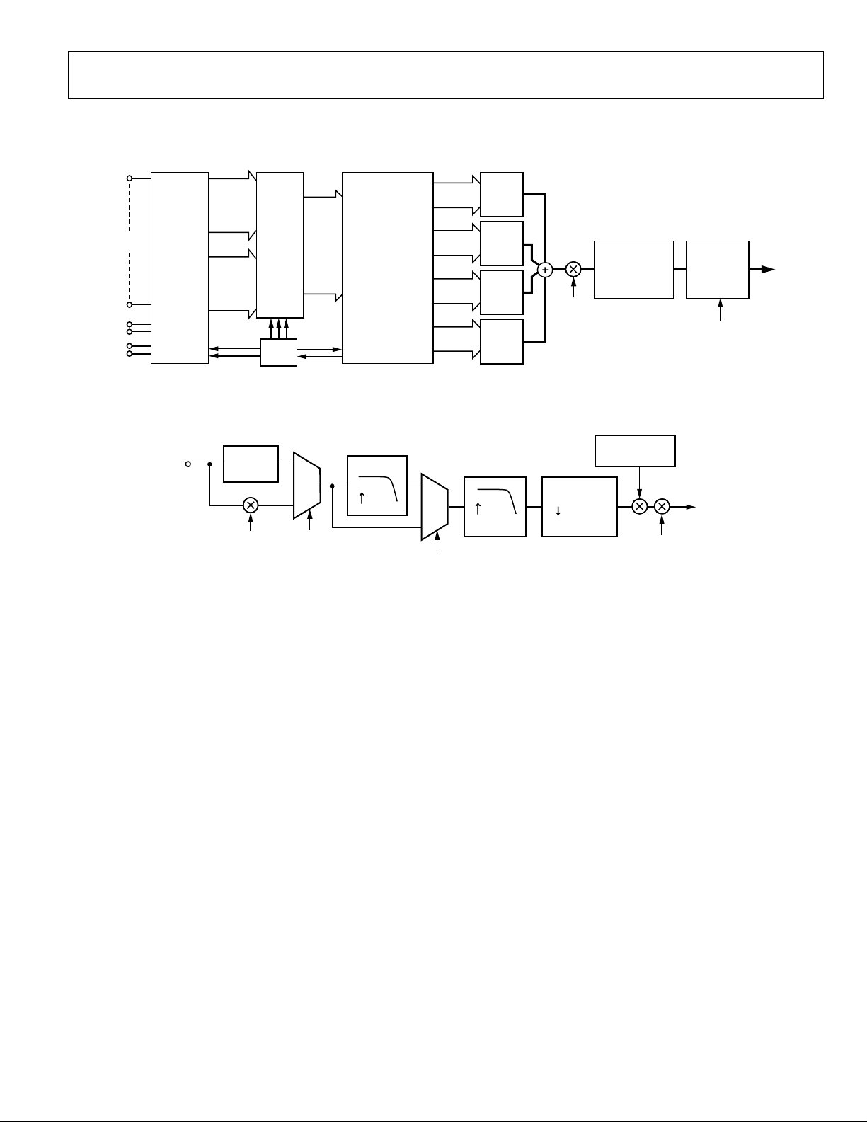
DETAILED FUNCTIONAL BLOCK DIAGRAMS
DATA-
PATH
0
DATA-
PATH
1
DATA-
PATH
2
DATA-
PATH
3
SUM
SCALE
16×
INTERPOLATOR
f
= 0 TO
C
f
DAC
BPF
BPF
/2
f
C
07852-002
32 INPUT
PINS
P0
P1
FS
DCO
LVD S/C MOS
CMOS
0TO 15
LVD S
RISE
CMOS
16 TO 31
LVD S
FALL
RETIMER
CLK
CTL
4TO
32 BITS
DATA FORMATTER/
ASSEMBLER
UP TO
32 BITS
UP TO
32 BITS
UP TO
32 BITS
UP TO
32 BITS
Figure 2. Digital Signal Processing Functional Block Diagram
24-BIT NCO
f
/16
0TO
QAM
MAPPER
INPUT
SCALE
BYPASS
QAM
SRRC
2
BYPASS
SRRC
RATE
N
2
(N = 0 TO 5) (P/Q = 0.5TO 1)
CONVERT ER
P/Q 24-BI T
Figure 3. Channel 0 Through Channel 3 Datapath Block Detail (I and Q Paths Are Identical So Only One Is Shown)
DAC
CH GAIN
0× TO 2×
07852-003
Rev. A | Page 3 of 76
Page 4

AD9789
SPECIFICATIONS
DC SPECIFICATIONS
AVDD33 = DVDD33 = 3.3 V, CVDD18 = DVDD18 = 1.8 V, DVDD15 = 1.5 V, f
Table 1.
Parameter Min Typ Max Unit
DAC RESOLUTION 14 Bits
ANALOG OUTPUTS
Offset Error 6.5 % FSR
Gain Error (with Internal Reference) 3.5 % FSR
Full-Scale Output Current (Monotonicity Guaranteed) 8.66 20.2 31.66 mA
Output Compliance Range −1.0 +1.0 V
Output Resistance 70 Ω
Output Capacitance 1 pF
TEMPERATURE DRIFT
Gain 135 ppm/°C
Reference Voltage 25 ppm/°C
REFERENCE
Internal Reference Voltage 1.2 V
Output Resistance1 5 kΩ
ANALOG SUPPLY VOLTAGES
AVDD33 3.14 3.3 3.47 V
CVDD18 1.71 1.8 1.89 V
DIGITAL SUPPLY VOLTAGES
DVDD33 3.14 3.3 3.47 V
DVDD18 1.71 1.8 1.89 V
DVDD15 1.43 1.5 1.58 V
SUPPLY CURRENTS AND POWER DISSIPATION
f
= 2.4 GSPS, f
DAC
I
45 mA
AVDD33
I
72 mA
DVDD18
I
180 mA
CVDD18
I
DVDD33
= 930 MHz, IFS = 25 mA, Four Channels Enabled
OUT
CMOS Interface 42 mA
LVDS Interface 16 mA
I
640 mA
DVDD15
f
= 2.0 GSPS, f
DAC
I
37.4 38.5 mA
AVDD33
I
67.3 70.5 mA
DVDD18
I
155.4 180 mA
CVDD18
I
40.3 50.7 mA
DVDD33
I
(Four Channels Enabled, All Signal Processing Enabled) 517 556 mA
DVDD15
I
(One Channel Enabled, 16× Interpolation Only) 365 391 mA
DVDD15
= 70 MHz, IFS = 20 mA, CMOS Interface
OUT
Power Dissipation
f
= 2.4 GSPS, f
DAC
= 930 MHz, IFS = 25 mA, Four Channels Enabled
OUT
CMOS Interface 1.7 W
LVDS Interface 1.63 W
1
Use an external amplifier to drive any external load.
= 2.4 GHz, IFS = 20 mA, unless otherwise noted.
DAC
Rev. A | Page 4 of 76
Page 5

AD9789
DIGITAL SPECIFICATIONS
AVDD33 = DVDD33 = 3.3 V, CVDD18 = DVDD18 = 1.8 V, DVDD15 = 1.5 V, f
are compliant with the IEEE Std 1596.3-1996 reduced range link, unless otherwise noted.
Table 2.
Parameter Min Typ Max Unit
CMOS DATA INPUTS (D[31:0], P0, P1)
Input Voltage High, VIH 2.0 3.3 V
Input Voltage Low, VIL 0 0.8 V
Input Current High, IIH −10 +10 µA
Input Current Low, IIL −10 +10 µA
Input Capacitance 2 pF
Setup Time, CMOS Data Input to CMOS_DCO1 5.3 ns
Hold Time, CMOS Data Input to CMOS_DCO1 −1.4 ns
CMOS OUTPUTS (CMOS_FS, CMOS_DCO)
Output Voltage High, VOH 2.4 3.3 V
Output Voltage Low, VOL 0 0.4 V
Output Current High, IOH 12 mA
Output Current Low, IOL 12 mA
Maximum Clock Rate (CMOS_DCO) 150 MHz
CMOS_DCO to CMOS_FS Delay 0.28 0.85 ns
LVDS DATA INPUTS (D[15:0]P, D[15:0]N, PARP, PARN)
Input Voltage Range, VIA or VIB 825 1575 mV
Input Differential Threshold, V
Input Differential Hysteresis, V
−100 +100 mV
IDTH
, V
IDTHH
25 mV
IDTHL
Input Differential Input Impedance, RIN 80 120 Ω
Maximum LVDS Input Rate 150 MSPS
Setup Time, LVDS Differential Input Data to Differential DCOx2 1.41 ns
Hold Time, LVDS Differential Input Data to Differential DCOx2 0.24 ns
LVDS OUTPUTS (DCOP, DCON, FSP, FSN)
DCOP, FSP = V
; DCON, FSN = VOB; 100 Ω Termination
OA
Output Voltage High, VOA or VOB 1375 mV
Output Voltage Low, VOA or VOB 1025 mV
Output Differential Voltage, |VOD| 150 200 250 mV
Output Offset Voltage, VOS 1150 1250 mV
Output Impedance, Single Ended, RO 40 140 Ω
RO Mismatch Between A and B, RO 10 %
Change in |VOD| Between 0 and 1, |VOD| 25 mV
Change in VOS Between 0 and 1, VOS 25 mV
Output Current—Driver Shorted to Ground, ISA, ISB 20 mA
Output Current—Drivers Shorted Together, I
4 mA
SAB
Power-Off Output Leakage, |IXA|, |IXB| 10 mA
Maximum Clock Rate (DCOP, DCON) 150 MHz
DCOx to FSx Delay 0.12 0.37 ns
DAC CLOCK INPUT (CLKP, CLKN)3
Differential Peak Voltage 1.4 1.8 V
Common-Mode Voltage 900 mV
DAC Clock Rate 2400 MHz
SERIAL PERIPHERAL INTERFACE
Maximum Clock Rate (f
Minimum Pulse Width High, t
Minimum Pulse Width Low, t
Minimum SDIO and CS to SCLK Setup, tDS
SCLK
, 1/t
) 25 MHz
SCLK
20 ns
PWH
20 ns
PWL
10 ns
= 2.4 GHz, IFS = 20 mA, LVDS drivers and receivers
DAC
Rev. A | Page 5 of 76
Page 6

AD9789
Parameter Min Typ Max Unit
Minimum SCLK to SDIO Hold, tDH 5 ns
Maximum SCLK to Valid SDIO and SDO, tDV 20 ns
Minimum SCLK to Invalid SDIO and SDO, t
INPUTS (SDIO, SCLK, CS)
Input Voltage High, VIH 2.0 3.3 V
Input Voltage Low, VIL 0 0.8 V
Input Current High, IIH −10 +10 µA
Input Current Low, IIL −10 +10 µA
OUTPUTS (SDO, SDIO)
Output Voltage High, VOH 2.4 3.6 V
Output Voltage Low, VOL 0 0.4 V
Output Current High, IOH 4 mA
Output Current Low, IOL 4 mA
1
See the CMOS Interface Timing section for more information.
2
See the LVDS Interface Timing section for more information.
3
See the Clock Phase Noise Effects on AC Performance section for more information.
AC SPECIFICATIONS
AVDD33 = DVDD33 = 3.3 V, CVDD18 = DVDD18 = 1.8 V, DVDD15 = 1.5 V, f
otherwise noted.
5 ns
DNV
= 2.4 GHz, IFS = 20 mA, digital scale = 0 dBFS, unless
DAC
Table 3.
Parameter Test Conditions/Comments Min Typ Max Unit
DYNAMIC PERFORMANCE
DAC Update Rate 2400 MSPS
Adjusted DAC Update Rate1 150 MSPS
Output Settling Time (tST) To 0.025% 13 ns
SPURIOUS-FREE DYNAMIC RANGE (SFDR)
f
= 2000 MSPS
DAC
f
= 100 MHz 70 dBc
OUT
f
= 316 MHz 63 dBc
OUT
f
= 550 MHz 58 dBc
OUT
f
= 2400 MSPS
DAC
f
= 100 MHz 70 dBc
OUT
f
= 316 MHz 70 dBc
OUT
f
= 550 MHz 60 dBc
OUT
f
= 850 MHz 60 dBc
OUT
= f
TWO-TONE INTERMODULATION DISTORTION
f
OUT2
+ 1.25 MHz
OUT1
(IMD)
f
= 2000 MSPS
DAC
f
= 100 MHz 86 dBc
OUT
f
= 316 MHz 73 dBc
OUT
f
= 550 MHz 62 dBc
OUT
f
= 2400 MSPS
DAC
f
= 100 MHz 86 dBc
OUT
f
= 316 MHz 74 dBc
OUT
f
= 550 MHz 66 dBc
OUT
f
= 850 MHz 66 dBc
OUT
NOISE SPECTRAL DENSITY (NSD)
1-Channel QAM f
f
= 100 MHz P
OUT
f
= 316 MHz P
OUT
f
= 550 MHz P
OUT
f
= 850 MHz P
OUT
= 2400 MSPS
DAC
= −14.5 dBm −167 dBm/Hz
OUT
= −15.5 dBm −166.5 dBm/Hz
OUT
= −18 dBm −166.5 dBm/Hz
OUT
= −18.5 dBm −166.5 dBm/Hz
OUT
Rev. A | Page 6 of 76
Page 7

AD9789
Parameter Test Conditions/Comments Min Typ Max Unit
ADJACENT CHANNEL LEAKAGE RATIO (ACLR)
= 2293.76 MSPS measured in 6 MHz
f
DAC
channels
1-Channel QAM
f
= 200 MHz (Harmonics) −76 dBc
OUT
f
= 200 MHz (Noise Floor) −82 dBc
OUT
f
= 500 MHz (Harmonics) −74.5 dBc
OUT
f
= 500 MHz (Noise Floor) −78 dBc
OUT
f
= 800 MHz (Harmonics) −69 dBc
OUT
f
= 800 MHz (Noise Floor) −78 dBc
OUT
2-Channel QAM
f
= 200 MHz (Harmonics) −77.5 dBc
OUT
f
= 200 MHz (Noise Floor) −81 dBc
OUT
f
= 500 MHz (Harmonics) −68 dBc
OUT
f
= 500 MHz (Noise Floor) −76 dBc
OUT
f
= 800 MHz (Harmonics) −66 dBc
OUT
f
= 800 MHz (Noise Floor) −76 dBc
OUT
4-Channel QAM
f
= 200 MHz (Harmonics) −75 dBc
OUT
f
= 200 MHz (Noise Floor) −76 dBc
OUT
f
= 500 MHz (Harmonics) −69 dBc
OUT
f
= 500 MHz (Noise Floor) −72 dBc
OUT
f
= 800 MHz (Harmonics) −67 dBc
OUT
f
= 800 MHz (Noise Floor) −72 dBc
OUT
WCDMA ACLR
= 2304 MSPS, mix mode second
f
DAC
Nyquist zone
Single Carrier f
= 1850 MHz
OUT
First Adjacent Channel −70 dBc
Second Alternate Channel −72.5 dBc
Third Alternate Channel −74 dBc
Single Carrier f
= 2100 MHz
OUT
First Adjacent Channel −68 dBc
Second Alternate Channel −70.4 dBc
Third Alternate Channel −72.7 dBc
Four Carrier f
= 2100 MHz
OUT
First Adjacent Channel −63.5 dBc
Second Alternate Channel −65.1 dBc
Third Alternate Channel −66.9 dBc
1
Adjusted DAC update rate is calculated as f
with f
= 2400 MSPS, F
DAC
= 2400 MSPS/16 = 150 MSPS.
DACadj
divided by the minimum required interpolation factor. For the AD9789, the minimum interpolation factor is 16. Thus,
DAC
Rev. A | Page 7 of 76
Page 8
AD9789
ABSOLUTE MAXIMUM RATINGS
Table 4.
Parameter Rating
AVDD33 to AVSS −0.3 V to +3.6 V
DVDD18 to DVSS −0.3 V to +1.98 V
DVDD33 to DVSS −0.3 V to +3.6 V
DVDD15 to DVSS −0.3 V to +1.98 V
CVDD18 to AVSS −0.3 V to +1.98 V
AVSS to DVSS −0.3 V to +0.3 V
CLKP, CLKN to AVSS −0.3 V to CVDD18 + 0.3 V
FS, DCO to DVSS −0.3 V to DVDD33 + 0.3 V
CMOS and LVDS Data Inputs
to DVSS
IOUTN, IOUTP to AVSS −1.0 V to AVDD33 + 0.3 V
I120, VREF, IPTAT to AVSS −0.3 V to AVDD33 + 0.3 V
IRQ, CS, SCLK, SDO, SDIO, RESET
to DVSS
Junction Temperature 150°C
Storage Temperature Range −65°C to +150°C
−0.3 V to DVDD33 + 0.3 V
−0.3 V to DVDD33 + 0.3 V
Stresses above those listed under Absolute Maximum Ratings
may cause permanent damage to the device. This is a stress
rating only; functional operation of the device at these or any
other conditions above those indicated in the operational
section of this specification is not implied. Exposure to absolute
maximum rating conditions for extended periods may affect
device reliability.
THERMAL RESISTANCE
θJA is specified for the worst-case conditions, that is, a device
soldered in a circuit board for surface-mount packages.
Table 5. Thermal Resistance
Package
Typ e
164-Ball
CSP_BGA
θJB θJC Unit Notes
θ
JA
25.5 14.4 6.8 °C/W 4-layer board, no vias
24.4 °C/W 4-layer board, 4 PCB vias
19.0 °C/W 8-layer board, 4 PCB vias
17.2 °C/W 8-layer board, 16 PCB vias
ESD CAUTION
Rev. A | Page 8 of 76
Page 9
AD9789
A
V
S
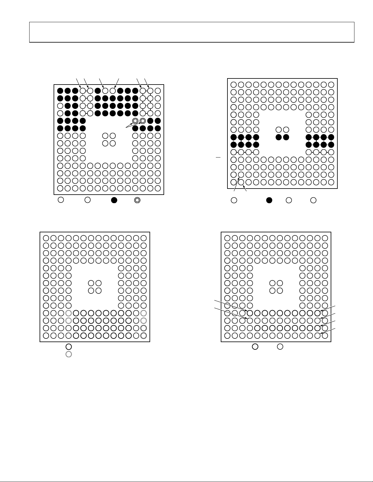
PIN CONFIGURATIONS AND FUNCTION DESCRIPTIONS
111312111089765243 4
A
B
C
D
E
F
G
++++ ++
H
J
K
XXXX
SB
NC
CS L
NC
CK
NC
DO
R
IO
I
RESET IRQ
NC
NC
NCNCNC
NC
DVSSNO CONNECT DVDD15DVDD33
X
++++
XXXX
+
07852-006
Figure 6. Digital Supply and SPI Pins (Top View)
CLKN C
CLKP D
CVDD18
111312111089765243 4
A
B
N
P
E
F
G
H
J
K
L
M
N
P
+
+
+
+
+
–
++
+
+
+
DVDD18
X
AVS S DV DD18CVDD18 AVDD33
DD33IOUTN IOUTP
XX
XX
XX
XX
NC
I120
VREF
IPTAT
CLK M
SDO N
SDIO P
07852-004
Figure 4. Clock and Analog Pins (Top View)
111312111089765243 4
A
B
C
D
E
F
G
H
J
K
P1
L
M
N
P
31 27 23 19 15 11 7 3
P0
30 26 22 18 14 10 6 2
29 25 21 17 13 9 5 1
28 24 20 16 12 8 4 0
D[31:0] CMOS D ATA INPUTS
PARITY AND CONTROL INPUTS
BU
CT
FS
DC
CMOS_BUS
CMOS_CTRL
CMOS_FS
CMOS_DCO
07852-005
PAR P
PARN
Figure 5. CMOS Mode Data Input Pins (Top View)
111312111089765243 4
A
B
C
D
E
F
G
H
J
K
P+
L
M
N
P
13 11 9
15
P–
15 13 11 9
14 12 10 8 6 4 2 0
14 12 10 8 6 4 2 0
14 14
+LVDS
7
7
–LVDS
531
531
FS
FS
DC
DC
FSP
FSN
DCOP
DCON
07852-007
Figure 7. LVDS Mode Data Input Pins (Top View)
Rev. A | Page 9 of 76
Page 10

AD9789
Table 6. Pin Function Descriptions
Pin No. Mnemonic Description
A1, A2, A3, A6, A9, A10, A11,
B1, B2, B3, B6, B7, B8, B9,
B10, B11, C2, C3, C6, C7, C8,
C9, C10, C11, D2, D3, D6, D7,
D8, D9, D10, D11, E1, E2, E3,
E4, E13, E14, F1, F2, F3, F4,
F11, F12, F13, F14
A4, A5, B4, B5, C4, C5, D4, D5 CVDD18 1.8 V Clock Supply.
A7 IOUTN DAC Negative Output Current.
A8 IOUTP DAC Positive Output Current.
A12, A13, B12, B13, C12, C13,
D12, D13
A14 NC No Connect. Leave floating.
B14 I120 Tie this pin to analog ground with a 10 kΩ resistor to generate a 120 µA reference current.
C1 CLKN Negative DAC Clock Input (DACCLK).
C14 VREF
D1 CLKP Positive DAC Clock Input (DACCLK).
D14 IPTAT
E11, E12 DVDD18 1.8 V Digital Supply.
G1, G2, G3, G4, G7, G8, G11,
G12, G13, G14
H1, H2, H3, H4, H7, H8, H11,
H12, H13, H14, J1, J2, J3, J4,
J11, J12, J13, J14
K1, K2, K3, K4, K11, K12, K13,
K14
L1
L2, L3, M2, M3, N3, N4, P3, P4 NC Not Used. Leave unconnected.
L4 P1/PARP CMOS/LVDS Parity Bit.
L5 D31/D15P CMOS/LVDS Data Input.
L6 D27/D13P CMOS/LVDS Data Input.
L7 D23/D11P CMOS/LVDS Data Input.
L8 D19/D9P CMOS/LVDS Data Input.
L9 D15/D7P CMOS/LVDS Data Input.
L10 D11/D5P CMOS/LVDS Data Input.
L11 D7/D3P CMOS/LVDS Data Input.
L12 D3/D1P CMOS/LVDS Data Input.
L13 FSP Positive LVDS Frame Sync (FSP) for Data Bus.
L14 CMOS_BUS
M1 SCLK Qualifying Clock for SPI.
M4 P0/PARN CMOS/LVDS Parity Bit.
M5 D30/D15N CMOS/LVDS Data Input.
M6 D26/D13N CMOS/LVDS Data Input.
M7 D22/D11N CMOS/LVDS Data Input.
M8 D18/D9N CMOS/LVDS Data Input.
M9 D14/D7N CMOS/LVDS Data Input.
M10 D10/D5N CMOS/LVDS Data Input.
M11 D6/D3N CMOS/LVDS Data Input.
M12 D2/D1N CMOS/LVDS Data Input.
M13 FSN Negative LVDS Frame Sync (FSN) for Data Bus.
AVSS Analog Supply Ground.
AVDD33 3.3 V Analog Supply.
Band Gap Voltage Reference I/O. Decouple to analog ground with a 1 nF capacitor.
Output impedance is approximately 5 kΩ.
Factory Test Pin. Output current, proportional to absolute temperature, is
approximately 10 µA at 25°C with a slope of approximately 20 nA/°C.
DVDD15 1.5 V Digital Supply.
DVSS Digital Supply Ground.
DVDD33 3.3 V Digital Supply.
CS
Active Low Chip Select for SPI.
Active High Input. Configures data bus for CMOS inputs. Low input configures data bus
to accept LVDS inputs.
Rev. A | Page 10 of 76
Page 11

AD9789
Pin No. Mnemonic Description
M14 CMOS_CTRL
N1 SDO Serial Data Output for SPI.
N2 RESET Active High Input. Resets the AD9789.
N5 D29/D14P CMOS/LVDS Data Input.
N6 D25/D12P CMOS/LVDS Data Input.
N7 D21/D10P CMOS/LVDS Data Input.
N8 D17/D8P CMOS/LVDS Data Input.
N9 D13/D6P CMOS/LVDS Data Input.
N10 D9/D4P CMOS/LVDS Data Input.
N11 D5/D2P CMOS/LVDS Data Input.
N12 D1/D0P CMOS/LVDS Data Input.
N13 DCOP Positive LVDS Data Clock Output (DCOP) for Data Bus.
N14 CMOS_FS CMOS Frame Sync for Data Bus.
P1 SDIO Serial Data Input/Output for SPI.
P2 IRQ
P5 D28/D14N CMOS/LVDS Data Input.
P6 D24/D12N CMOS/LVDS Data Input.
P7 D20/D10N CMOS/LVDS Data Input.
P8 D16/D8N CMOS/LVDS Data Input.
P9 D12/D6N CMOS/LVDS Data Input.
P10 D8/D4N CMOS/LVDS Data Input.
P11 D4/D2N CMOS/LVDS Data Input.
P12 D0/D0N CMOS/LVDS Data Input.
P13 DCON Negative LVDS Data Clock Output (DCON) for Data Bus.
P14 CMOS_DCO CMOS Data Clock Output for Data Bus.
Active High Input. Enables CMOS_DCO and CMOS_FS signals and disables DCOP/DCON
and FSP/FSN signals. Low input disables CMOS_DCO and CMOS_FS signals and enables
DCOP/DCON and FSP/FSN signals.
Active Low, Open-Drain Interrupt Request Output. Pull up to DVDD33 with a 10 kΩ
resistor.
Rev. A | Page 11 of 76
Page 12
AD9789
–
–
–
–
–
–
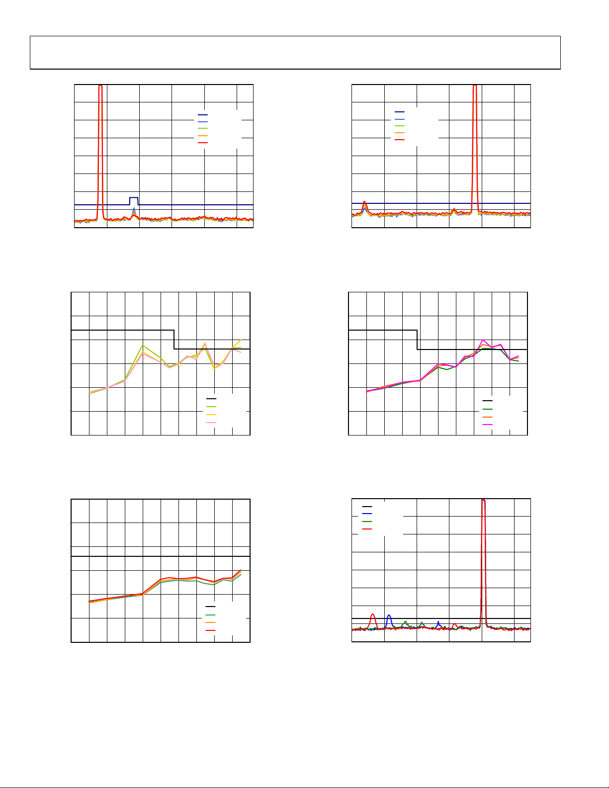
TYPICAL PERFORMANCE CHARACTERISTICS
40
–45
–50
–55
–60
–65
–70
SFDR (dBc)
–75
–80
–85
–90
0 200 400 600 800 1000 1200
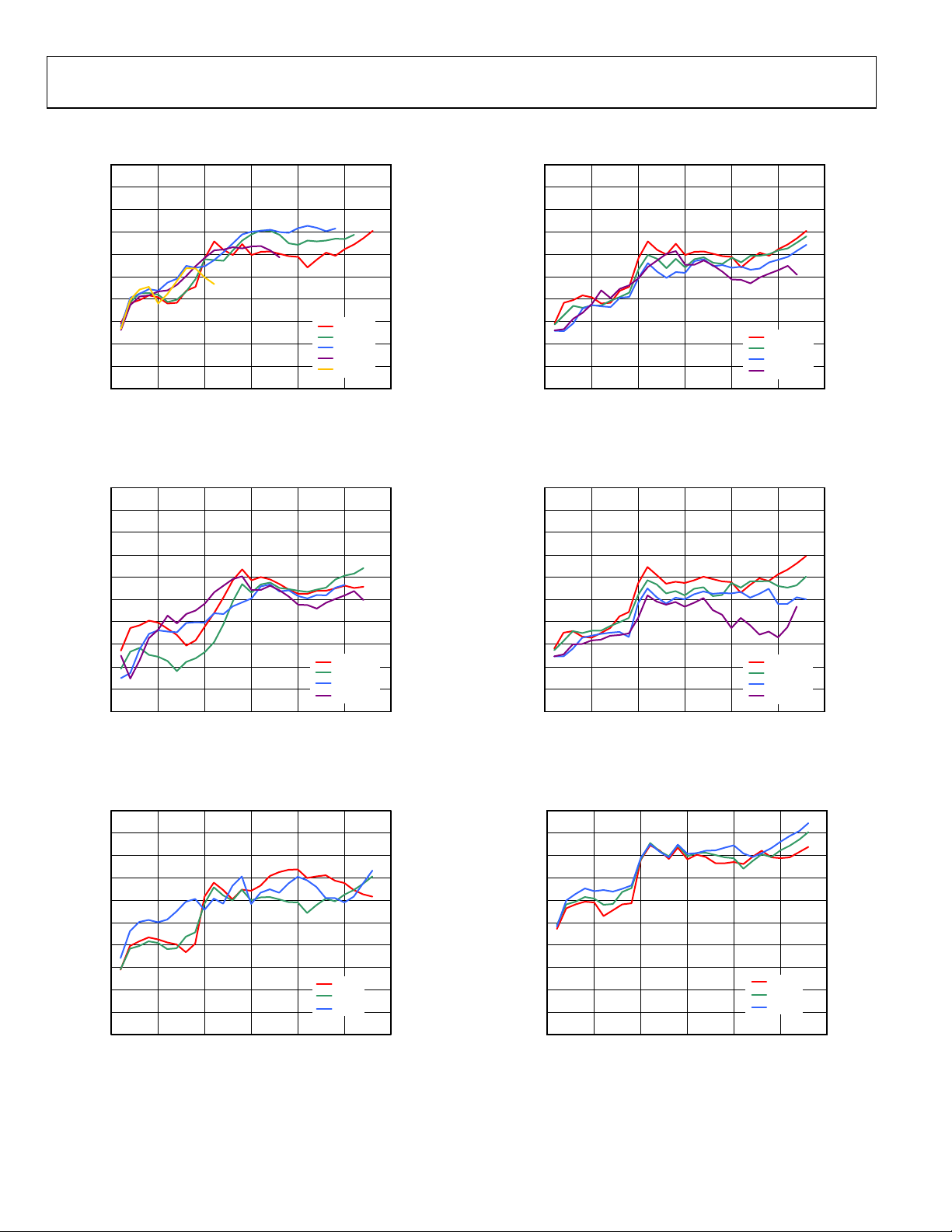
Figure 8. SFDR vs. f
OUT
f
(MHz)
OUT
over f
, Full-Scale Current = 20 mA,
DAC
2.4GHz
2.2GHz
2GHz
1.6GHz
1GHz
Digital Scale = 0 dBFS, Temperature = 25°C
07852-013
40
–45
–50
–55
–60
–65
–70
SFDR (dBc)
–75
–80
–85
–90
0 200 400 600 800 1000 1200
Figure 11. SFDR vs. f
f
(MHz)
OUT
over Digital Full Scale, f
OUT
0dBFS
–3dBFS
–6dBFS
–12dBFS
= 2.4 GHz,
DAC
Full-Scale Current = 20 mA, Temperature = 25°C
07852-010
40
–45
–50
–55
–60
–65
–70
–75
HARMONIC LEVEL (dBc)
–80
–85
–90
0 200 400 600 800 1000 1200
Figure 9. Second-Order Harmonic vs. f
= 2.4 GHz, Full-Scale Current = 20 mA, Temperature = 25°C
f
DAC
40
–45
–50
–55
–60
–65
–70
SFDR (dBc)
–75
–80
–85
–90
0 200 400 600 800 1000 1200
Figure 10. SFDR vs. f
f
(MHz)
OUT
over Digital Full Scale,
OUT
f
(MHz)
OUT
over Full-Scale Current, f
OUT
0dBFS
–3dBFS
–6dBFS
–12dBFS
32mA
20mA
8mA
DAC
Digital Scale = 0 dBFS, Temperature = 25°C
= 2.4 GHz,
40
–45
–50
–55
–60
–65
–70
–75
HARMONIC LEVEL (dBc)
–80
–85
–90
07852-009
0 200 400 600 800 1000 1200
Figure 12. Third-Order Harmonic vs. f
= 2.4 GHz, Full-Scale Current = 20 mA, Temperature = 25°C
f
DAC
50
–55
–60
–65
–70
–75
–80
SFDR (dBc)
–85
–90
–95
–100
07852-011
0 200 400 600 800 1000 1200
Figure 13. SFDR vs. f
f
(MHz)
OUT
OUT
f
(MHz)
OUT
over Temperature, f
OUT
over Digital Full Scale,
0dBFS
–3dBFS
–6dBFS
–12dBFS
+85°C
+25°C
–40°C
= 2.4 GHz,
DAC
07852-012
07852-008
Full-Scale Current = 20 mA, Digital Scale = 0 dBFS
Rev. A | Page 12 of 76
Page 13
AD9789
–
–
90
100
80
70
60
IMD (dBc)
50
40
30
0 100 200 300 400 500 600 700 800 900 1000 1100
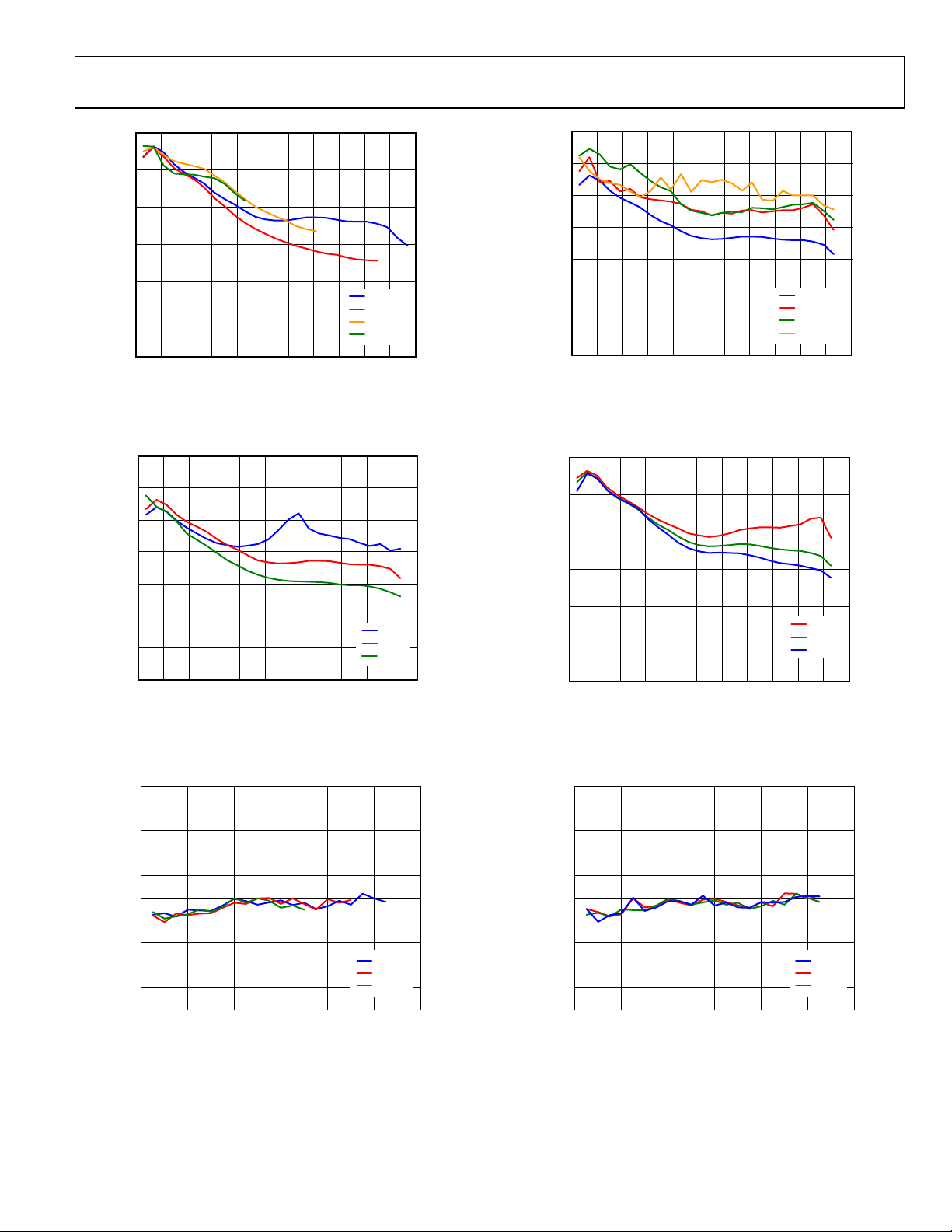
Figure 14. Third-Order IMD vs. f
f
OUT
OUT
(MHz)
over f
, Full-Scale Current = 20 mA,
DAC
Digital Scale = 0 dBFS, Temperature = 25°C
100
90
80
70
60
IMD (dBc)
50
40
30
0 100 200 300 400 500 600 700 800 900 1000 1100
Figure 15. Third-Order IMD vs. f
f
(MHz)
OUT
over Full-Scale Current, f
OUT
Digital Scale = 0 dBFS, Temperature = 25°C
2.4GHz
2.0GHz
1.6GHz
1.0GHz
32mA
20mA
8mA
DAC
07852-034
07852-038
= 2.4 GHz,
90
80
70
60
IMD (dBc)
50
40
30
0 100 200 300 400 500 600 700 800 900 1000 1100
Figure 17. Third-Order IMD vs. f
f
(MHz)
OUT
over Digital Full Scale, f
OUT
Full-Scale Current = 20 mA, Temperature = 25°C
90
80
70
60
IMD (dBc)
50
40
30
0 100 200 300 400 500 600 700 800 900 1000 1100
Figure 18. Third-Order IMD vs. f
f
(MHz)
OUT
over Temperature, f
OUT
Full-Scale Current = 20 mA, Digital Scale = 0 dBFS
0dBFS
–3dBFS
–6dBFS
–12dBFS
DAC
+85°C
+25°C
–40°C
= 2.4 GHz,
DAC
07852-037
= 2.4 GHz,
07852-041
155
–157
–159
–161
–163
–165
–167
NSD (dBm/Hz)
–169
–171
–173
–175
0 200 400 600 800 1000 1200
Figure 16. NSD vs. f
OUT
f
(MHz)
OUT
over f
, 1-Channel QAM, Full-Scale Current = 20 mA
DAC
2.4GHz
2.0GHz
1.6GHz
07852-016
155
–157
–159
–161
–163
–165
–167
NSD (dBm/Hz)
–169
–171
–173
–175
0 200 400 600 800 1000 1200
Figure 19. NSD vs. f
over Temperature, 1-Channel QAM, f
OUT
f
OUT
(MHz)
+85°C
+25°C
–40°C
= 2.4 GHz,
DAC
07852-019
Full-Scale Current = 20 mA
Rev. A | Page 13 of 76
Page 14
AD9789
–
–
–
–15
–25
–35
–5
DOCSIS3
–40°C
0°C
+25°C
+85°C
–15
–25
–35
–5
DOCSIS3
–40°C
0°C
+25°C
+85°C
–45
ACLR (dB c)
–55
–65
–75
–85
50 250 450 650 850
FREQUENCY (MHz)
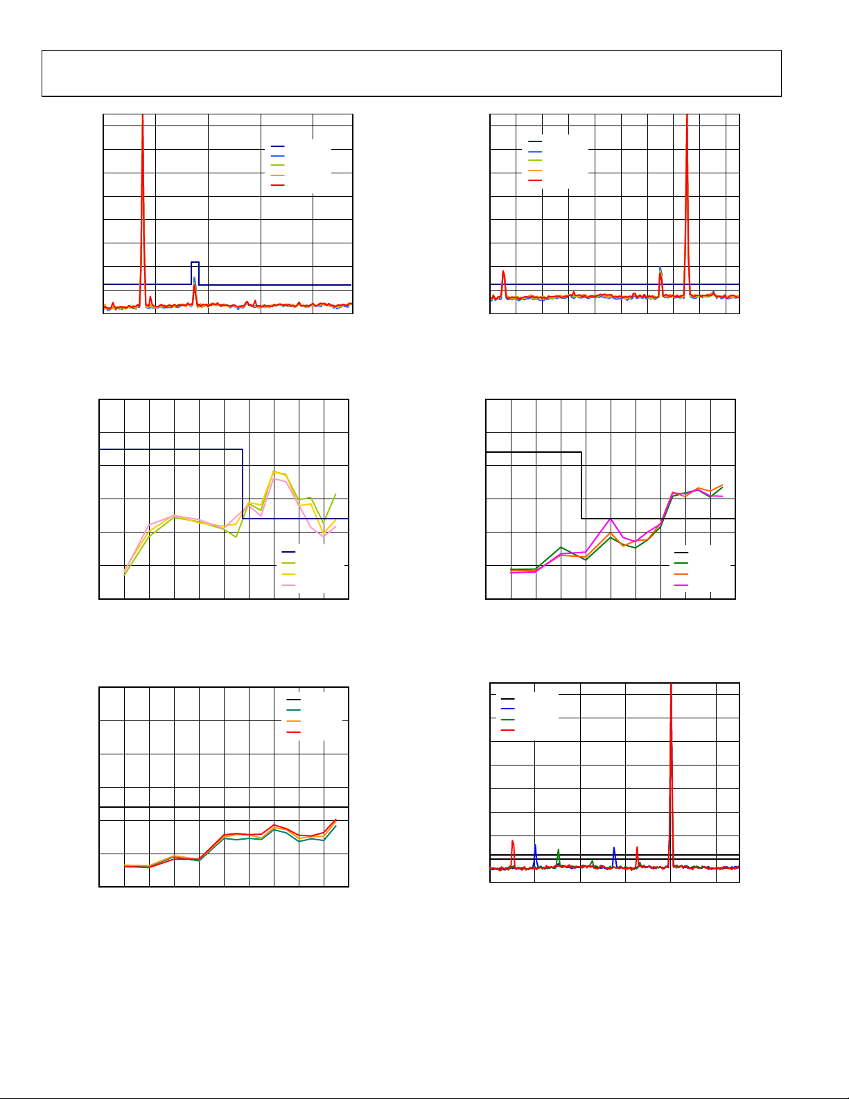
Figure 20. ACLR Performance over Temperature, 1-Channel QAM,
= 2.3 GHz, Full-Scale Current = 20 mA, f
f
DAC
= 200 MHz, Sum Scale = 48
OUT
(DOCSIS SPEC Is −73 dBc; Harmonic Exception Is −63 dBc)
55
–60
–65
–70
–75
HARMONIC LEVEL (dBc)
–80
–85
0 100 200 300 400 500 600 700 800 900 1000
f
(MHz)
OUT
Figure 21. Second-Order Harmonic Performance vs. f
1-Channel QAM, f
= 2.3 GHz, Full-Scale Current = 20 mA, Sum Scale = 48
DAC
DOCSIS3
25°C
65°C
85°C
over Temperature,
OUT
(DOCSIS SPEC Is −73 dBc; Harmonic Exception Is −63 dBc)
55
–60
–65
–70
ACLR (d Bc)
–75
–80
–85
0 100 200 300 400 500 600 700 800 900 1000
Figure 22. Noise Floor vs. f
1-Channel QAM, f
= 2.3 GHz, Full-Scale Current = 20 mA, Sum Scale = 48
DAC
OUT
f
(MHz)
OUT
over Temperature (ACLR Measured Beyond 30 MHz),
(DOCSIS SPEC Is −73 dBc)
DOCSIS3
25°C
65°C
85°C
–45
ACLR (dB c)
–55
–65
–75
–85
50 150 250 350 450 550 650 750 850 950
07852-015
FREQUENCY (MHz)
07852-018
Figure 23. ACLR Performance over Temperature, 1-Channel QAM,
= 2.3 GHz, Full-Scale Current = 20 mA, f
f
DAC
= 800 MHz, Sum Scale = 48
OUT
(DOCSIS SPEC Is −73 dBc)
55
–60
–65
–70
–75
HARMONIC LEVEL (dBc)
–80
–85
0 100 200 300 400 500 600 700 800 900 1000
07852-014
f
(MHz)
OUT
Figure 24. Third-Order Harmonic Performance vs. f
1-Channel QAM, f
= 2.3 GHz, Full-Scale Current = 20 mA, Sum Scale = 48
DAC
DOCSIS3
25°C
65°C
85°C
over Temperature,
OUT
07852-017
(DOCSIS SPEC Is −73 dBc; Harmonic Exception Is −63 dBc)
–5
DOCSIS 3
–15
–25
–35
–45
ACLR (dB c)
–55
–65
–75
–85
07852-031
Figure 25. ACLR Performance over f
2.3GHz
2.2GHz
2.4GHz
50 250 450 650 850 1050
FREQUENCY (MHz)
, 1-Channel QAM, f
DAC
= 850 MHz,
OUT
07852-039
Full-Scale Current = 20 mA, Temperature = 25°C, Sum Scale = 48
(DOCSIS SPEC Is −73 dBc)
Rev. A | Page 14 of 76
Page 15
AD9789
–
–
–
0
DOCSIS3
CMOS
LVD S
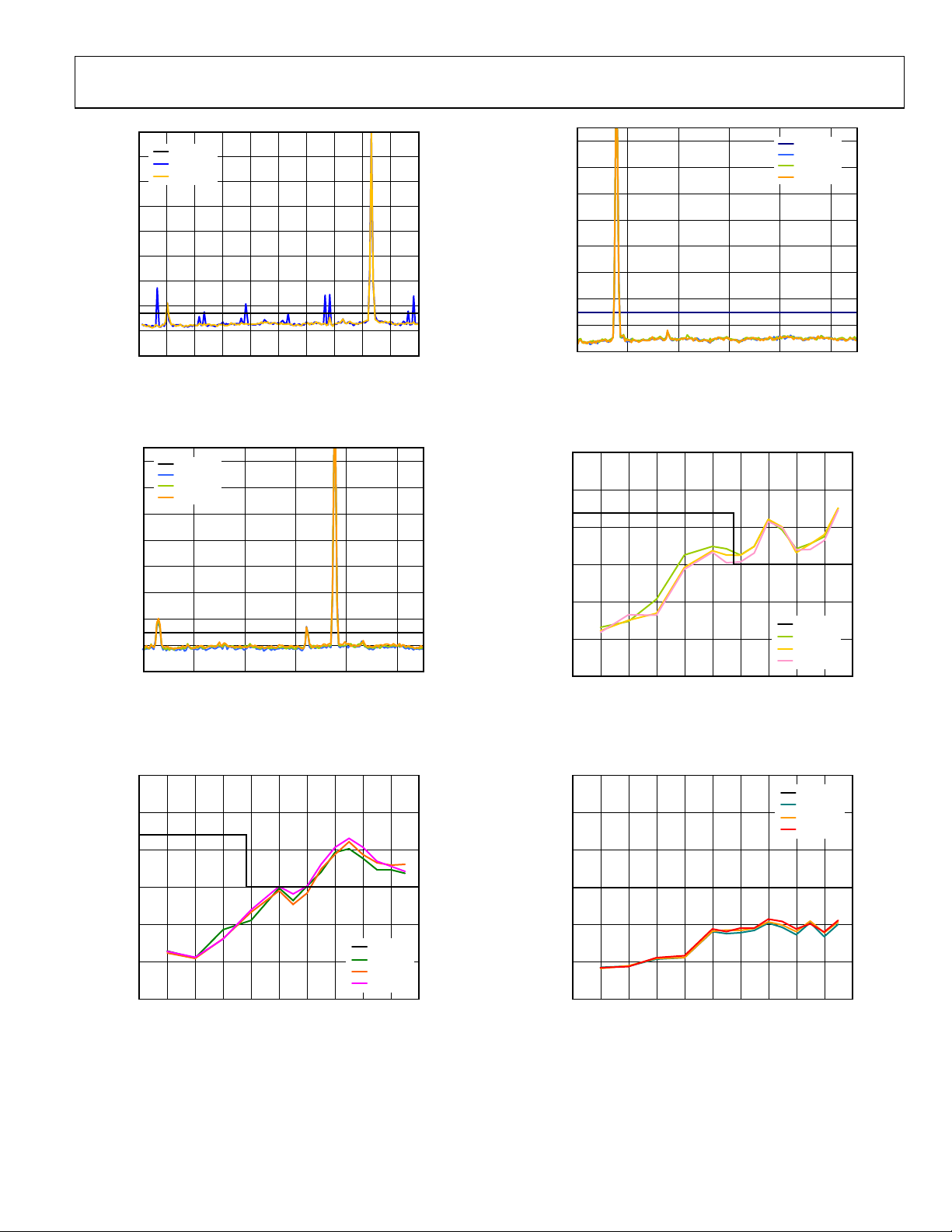
0 100 200 300 400 500 600 700 800 900 1000
FREQUENCY ( MHz)
07852-040
ACLR (dBc)
–10
–20
–30
–40
–50
–60
–70
–80
–90
Figure 26. ACLR Performance for CMOS and LVDS Interfaces, 1-Channel QAM,
= 840 MHz, f
f
OUT
= 2.4 GHz, Full-Scale Current = 20 mA, Sum Scale = 48
DAC
(DOCSIS SPEC Is −73 dBc)
–5
–15
–25
–35
–45
ACLR (dB c)
–55
–65
–75
–85
DOCSIS3
25°C
65°C
85°C
50 250 450 650 850 1050
FREQUENCY (MHz)
07852-042
Figure 27. ACLR Performance over Temperature, 2-Channel QAM,
f
= 800 MHz, f
OUT
= 2.3 GHz, Full-Scale Current = 25 mA, Sum Scale = 32
DAC
(DOCSIS SPEC Is −70 dBc)
55
–60
–65
–5
–15
–25
–35
–45
ACLR (dB c)
–55
–65
–75
–85
50 250 450 650 850 1050
FREQUENCY (MHz)
DOCSIS3
25°C
65°C
85°C
07852-044
Figure 29. ACLR Performance over Temperature, 2-Channel QAM,
= 200 MHz, f
f
OUT
= 2.3 GHz, Full-Scale Current = 25 mA, Sum Scale = 32
DAC
(DOCSIS SPEC Is −70 dBc; Harmonic Exception Is −63 dBc)
55
–60
–65
–70
–75
HARMONIC LEVEL (dBc)
–80
–85
0 100 200 300 400 500 600 700 800 900 1000
f
OUT
(MHz)
Figure 30. Second Harmonic Performance vs. f
2-Channel QAM, f
= 2.3 GHz, Full-Scale Current = 25 mA, Sum Scale = 32
DAC
DOCSIS3
25°C
65°C
85°C
over Temperature,
OUT
07852-045
(DOCSIS SPEC Is −70 dBc; Harmonic Exception Is −63 dBc)
55
DOCSIS3
–60
–65
25°C
65°C
85°C
–70
–75
HARMONIC LEVEL (dBc)
–80
–85
0 100 200 300 400 500 600 700 800 900 1000
f
OUT
(MHz)
Figure 28. Third-Order Harmonic Performance vs. f
2-Channel QAM, f
= 2.3 GHz, Full-Scale Current = 25 mA, Sum Scale = 32
DAC
(DOCSIS SPEC Is −70 dBc; Harmonic Exception Is −63 dBc)
DOCSIS3
25°C
65°C
85°C
over Temperature,
OUT
07852-043
–70
ACLR (d Bc)
–75
–80
–85
0 100 200 300 400 500 600 700 800 900 1000
Figure 31. Noise Floor vs. f
2-Channel QAM, f
= 2.3 GHz, Full-Scale Current = 25 mA, Sum Scale = 32
DAC
f
(MHz)
OUT
over Temperature (ACLR Measured Beyond 30 MHz),
OUT
(DOCSIS SPEC Is −70 dBc)
07852-046
Rev. A | Page 15 of 76
Page 16
AD9789
–
–
–
0
–10
–20
–30
–40
ACLR (dBc)
–50
–60
–70
–80
50 250 450 650 850 1050
FREQUENCY ( MHz)
DOCSIS3
–40°C
0°C
+25°C
+85°C
Figure 32. ACLR Performance over Temperature, 4-Channel QAM,
= 200 MHz, f
f
OUT
= 2.3 GHz, Full-Scale Current = 25 mA, Sum Scale = 20
DAC
(DOCSIS SPEC Is −67 dBc; Harmonic Exception Is −63 dBc)
55
–60
–65
–70
0
–10
–20
–30
–40
ACLR (dBc)
–50
–60
–70
–80
50 250 450 650 850 1050
07852-027
DOCSIS3
–40°C
0°C
+25°C
+85°C
FREQUENCY (MHz )
07852-030
Figure 35. ACLR Performance over Temperature, 4-Channel QAM,
= 800 MHz, f
f
OUT
= 2.3 GHz, Full-Scale Current = 25 mA, Sum Scale = 20
DAC
(DOCSIS SPEC Is −67 dBc)
55
–60
–65
–70
–75
HARMONIC LEVEL (dBc)
–80
–85
0 100 200 300 400 500 600 700 800 900 1000
f
(MHz)
OUT
Figure 33. Second-Order Harmonic Performance vs. f
4-Channel QAM, f
= 2.3 GHz, Full-Scale Current = 25 mA, Sum Scale = 20
DAC
(DOCSIS SPEC Is −67 dBc; Harmonic Exception Is −63 dBc)
55
–60
–65
–70
ACLR (d Bc)
–75
–80
–85
0 100 200 300 400 500 600 700 800 900 1000
Figure 34. Noise Floor vs. f
4-Channel QAM, f
= 2.3 GHz, Full-Scale Current = 25 mA, Sum Scale = 20
DAC
OUT
f
(MHz)
OUT
over Temperature (ACLR Measured Beyond 30 MHz),
(DOCSIS SPEC Is −67 dBc)
DOCSIS3
25°C
65°C
85°C
over Temperature,
OUT
DOCSIS3
25°C
65°C
85°C
–75
HARMONIC LEVEL (dBc)
–80
–85
0 100 200 300 400 500 600 700 800 900 1000
07852-026
f
(MHz)
OUT
Figure 36. Third-Order Harmonic Performance vs. f
4-Channel QAM, f
= 2.3 GHz, Full-Scale Current = 25 mA, Sum Scale = 20
DAC
DOCSIS 3
25°C
65°C
85°C
over Temperature,
OUT
07852-029
(DOCSIS SPEC Is −67 dBc; Harmonic Exception Is −63 dBc)
0
DOCSIS3
–10
–20
–30
–40
ACLR (dBc)
–50
–60
–70
–80
07852-028
Figure 37. ACLR Performance over f
2.3GHz
2.2GHz
2.4GHz
50 250 450 650 850 1050
FREQUENCY (MHz )
, 4-Channel QAM, f
DAC
= 850 MHz,
OUT
07852-047
Full-Scale Current = 25 mA, Temperature = 25°C, Sum Scale = 20
(DOCSIS SPEC Is −67 dBc)
Rev. A | Page 16 of 76
Page 17
AD9789
A
m
A
m
A
m
A
m
TTEN 2dBRE F –32.76dB
TTEN 2dBRE F –32.76dB
CENTER 840.00MHz
RES BW 56kHz VBW 560kHz
FREQ. LOWER UPPER
RMS RESULTS
CARRIER POWER
–18.10dBm/
6.00000MHz
OFFSET REF BW dBc dBm dBc dBm
3.375MHz 750.0kHz –65.57 –83.66 –68. 98 –87.07
6.375MHz 5.250M Hz –75.01 –93. 11 –74.62 –92.71
12.00MHz 6.000M Hz –76.83 –94.92 –76.46 –94.55
18.00MHz 6.000M Hz –77.17 –95.26 –76.56 –94.66
Figure 38. 1-Channel QAM ACLR, f
SWEEP 39. 12ms (601 PTS)
= 840 MHz, Temperature = 25°C,
OUT
SPAN 42MHz
Sum Scale = 48, Full-Scale Current = 20 mA, Span = 42 MHz
TTEN 2dBRE F –35.91dB
CENTER 840.00MHz
RES BW 30kHz VBW 300kHz
FREQ. LOWER UPPER
RMS RESULTS
CARRIER POWER
–21.75dBm/
6.00000MHz
OFFSET REF BW dBc dBm dBc dBm
3.375MHz 750.0kHz –71.64 –93.39 –72. 50 –94.25
6.375MHz 5.250M Hz –73.71 –95.47 –66.72 –88.47
12.00MHz 6.000M Hz –73.58 –95.33 0.50 –21.10
18.00MHz 6.000M Hz –73.70 –95.45 –66.72 –88.48
Figure 39. 2-Channel QAM ACLR, f
SWEEP 136. 2ms (601 PTS)
= 840 MHz, Sum Scale = 32,
OUT
SPAN 42MHz
Full-Scale Current = 25 mA, Span = 42 MHz, Channel 1
CENTER 840.00MHz
RES BW 30kHz VBW 300kHz
FREQ. LOWER UPPER
RMS RESULTS
CARRIER POWER
–17.98dBm/
07852-020
6.00000MHz
OFFSET REF BW dBc dBm dBc dBm
3.375MHz 750.0kHz –73.99 –91.97 –74. 93 –92.91
6.375MHz 5.250M Hz –74.94 –92.92 –75.35 –93.33
Figure 40. 1-Channel QAM ACLR, f
SWEEP 58.4ms (601 PTS)
= 840 MHz, Temperature = 25°C,
OUT
SPAN 18MHz
7852-023
Sum Scale = 48, Full-Scale Current = 20 mA, Span = 18 MHz
TTEN 2dBRE F –35.91dB
START 831.00M Hz
RES BW 30kHz VBW 300kHz
FREQ. LOWER UPPER
RMS RESULTS
CARRIER POWER
–21.29dBm/
07852-061
6.00000MHz
OFFSET REF BW dBc dBm dBc dBm
3.375MHz 750.0kHz –70.07 –92.16 –73. 20 –94.49
6.375MHz 5.250M Hz –69.05 –90.34 –73.87 –95.16
12.00MHz 6.000M Hz –0.49 –21.78 –73.29 –94.58
18.00MHz 6.000M Hz –66.61 –87.90 –73.98 –95.27
Figure 41. 2-Channel QAM ACLR, f
SWEEP 136. 2ms (601 PTS)
= 840 MHz, Sum Scale = 32,
OUT
STOP 873MHz
07852-066
Full-Scale Current = 25 mA, Span = 42 MHz, Channel 2
Rev. A | Page 17 of 76
Page 18
AD9789
A
m
A
m
A
m
A
TTEN 2dBRE F –35.91dB
TTEN 2dBRE F –35.91dB
CENTER 840.00MHz
RES BW 30kHz VBW 300kHz
FREQ. LOWER UPPER
RMS RESULTS
CARRIER POWER
–21.56dBm/
6.00000MHz
OFFSET REF BW dBc dBm dBc dBm
3.375MHz 750.0kHz –75.37 –96.93 –75. 56 –97. 11
6.375MHz 5.250M Hz –73.85 –95.41 –72.54 –94.10
Figure 42. Zoomed 2-Channel QAM ACLR, f
SWEEP 58.4ms (601 PTS)
OUT
SPAN 18MHz
= 840 MHz, Sum Scale = 32,
Full-Scale Current = 25 mA, Span = 18 MHz, Channel 1
TTEN 2dBRE F –35.96dB
CENTER 834.00MHz
RES BW 30kHz
RMS RESULTS
CARRIER POWER
–23.63dBm/
6.00000MHz
VBW 300kHz
FREQ. LOWER UPPER
OFFSET REF BW dBc dBm dBc dBm
3.375MHz 750.0kHz –70.33 –93.96 – 11.07 –34.70
6.375MHz 5.250MHz –69.04 –92.67 –0.49 –24.12
12.00MHz 6.000MHz –70.38 –94.01 0.00 –23.63
18.00MHz 6.000MHz –71.02 –94.65 0.43 –23.20
Figure 43. 4-Channel QAM ACLR, f
SWEEP 136.2ms (601 PTS)
= 840 MHz, Temperature = 25°C,
OUT
SPAN 42MHz
Sum Scale = 20, Full-Scale Current = 25 mA, Span = 42 MHz, Channel 1
CENTER 852.00MHz
RES BW 30kHz VBW 300kHz
FREQ. LOWER UPPER
RMS RESULTS
CARRIER POWER
–21.03dBm/
07852-065
6.00000MHz
OFFSET REF BW dBc dBm dBc dBm
3.375MHz 750.0kHz –75.51 –96.54 –75. 17 –96.20
6.375MHz 5.250M Hz –72.55 –93.58 –73.90 –94.93
Figure 44. Zoomed 2-Channel QAM ACLR, f
SWEEP 58.4ms (601 PTS)
OUT
SPAN 18MHz
07852-067
= 840 MHz, Sum Scale = 32,
Full-Scale Current = 25 mA, Span = 18 MHz, Channel 2
TTEN 2dBREF –35.96dBm
CENTER 852.00MHz
RES BW 30kHz
RMS RESULTS
CARRIER POWER
–23.23dBm/
07852-021
6.00000MHz
Figure 45. 4-Channel QAM ACLR, f
VBW 300kHz
FREQ. LOWER UPPER
OFFSET REF BW dBc dBm dBc dBm
3.375MHz 750.0kHz –11.10 –34.32 –72.19 –95.42
6.375MHz 5.250M Hz –0.75 –23.98 –68.97 –92.20
12.00MHz 6.000M Hz –0.59 –23.81 –70.32 –93.55
18.00MHz 6.000M Hz –0.35 –23.58 –70.70 –93.93
SWEEP 136. 2ms (601 PTS)
= 840 MHz, Temperature = 25°C,
OUT
SPAN 42MHz
07852-022
Sum Scale = 20, Full-Scale Current = 25 mA, Span = 42 MHz, Channel 4
Rev. A | Page 18 of 76
Page 19
AD9789
A
A
TTEN 2dBREF –35.96dBm
TTEN 2dBREF –35.96dBm
CENTER 834.00MHz
RES BW 30kHz
RMS RESULTS
CARRIER POWER
–23.62dBm/
6.00000MHz
VBW 300kHz
FREQ. LOWER UPPER
OFFSET REF BW dBc dBm dBc dBm
3.375MHz 750.0kHz –72.95 –96.56 –10. 86 –34.48
6.375MHz 5.250M Hz –69.38 –92.99 –0.51 –24.13
Figure 46. Zoomed 4-Channel QAM ACLR, f
SWEEP 58.4ms (601 PTS)
OUT
SPAN 18MHz
= 840 MHz, Temperature =
07852-024
25°C, Sum Scale = 20, Full-Scale Current = 25 mA, Span = 18 MHz, Channel 1
50
48
46
44
42
40
MER (dB)
38
36
34
32
30
50 150 250 350 450 550 650 750 850 950
f
OUT
(MHz)
+25°C
+85°C
–40°C
07852-032
Figure 47. Modulation Error Ratio, Equalized, 1-Channel 256-QAM,
f
= 2.29376 GHz, Full-Scale Current = 20 mA, Sum Scale = 48
DAC
(Equalization Filter from Demodulation Toolbox on Spectrum Analyzer Used)
50
48
46
44
42
40
MER (dB)
38
36
34
32
30
50 150 250 350 450 550 650 750 850 950
f
OUT
(MHz)
+25°C
+85°C
–40°C
07852-033
Figure 48. Modulation Error Ratio, Unequalized, 1-Channel 256-QAM,
= 2.29376 GHz, Full-Scale Current = 20 mA, Sum Scale = 48
f
DAC
CENTER 852.00MHz
RES BW 30kHz
RMS RESULTS
CARRIER POWER
–23.20dBm/
6.00000MHz
VBW 300kHz
FREQ. LOWER UPPER
OFFSET REF BW dBc dBm dBc dBm
3.375MHz 750.0kHz –11.20 –34.40 –74.44 –97.64
6.375MHz 5.250M Hz –0.77 –23.96 –69.07 –92.26
Figure 49. Zoomed 4-Channel QAM ACLR, f
SWEEP 58.4ms (601 PTS)
OUT
SPAN 18MHz
= 840 MHz, Temperature =
07852-025
25°C, Sum Scale = 20, Full-Scale Current = 25 mA, Span = 18 MHz, Channel 4
50
48
46
44
42
40
MER (dB)
38
36
34
32
30
50 150 250 350 450 550 650 750 850 950
f
OUT
(MHz)
+25°C
+85°C
–40°C
07852-035
Figure 50. Modulation Error Ratio, Equalized, 4-Channel 256-QAM,
f
= 2.29376 GHz, Full-Scale Current = 25 mA, Sum Scale = 20
DAC
(Equalization Filter from Demodulation Toolbox on Spectrum Analyzer Used)
50
48
46
44
42
40
MER (dB)
38
36
34
32
30
50 150 250 350 450 550 650 750 850 950
f
OUT
(MHz)
+25°C
+85°C
–40°C
07852-036
Figure 51. Modulation Error Ratio, Unequalized, 4-Channel 256-QAM,
= 2.29376 GHz, Full-Scale Current = 25 mA, Sum Scale = 20
f
DAC
Rev. A | Page 19 of 76
Page 20
AD9789
–
A
m
A
m
80
75
70
65
60
55
50
45
40
SFDR (dBc)
35
30
25
20
15
10
1200 1300 1400 1500 1600 1700 1800 1900 2000 2100 2200 2300 2400
Figure 52. SFDR vs. f
in Mix Mode, f
OUT
f
(MHz)
OUT
= 2.4 GHz, Full-Scale Current = 20 mA
DAC
(Second Nyquist Zone Performance)
90
85
80
75
70
65
60
55
IMD (dBc)
50
45
40
35
30
1200 1300 1400 1500 1600 1700 1800 1900 2000 2100 2200 2300 2400
Figure 53. IMD vs. f
in Mix Mode, f
OUT
f
(MHz)
OUT
= 2.4 GHz, Full-Scale Current = 20 mA
DAC
(Second Nyquist Zone Performance)
07852-068
CENTER 2.100G Hz
RES BW 30kHz VBW 300kHz
RMS RESULTS
CARRIER POWER
–19.95dBm/
3.84000MHz
Figure 55. One-Carrier WCDMA ACLR in Mix Mode, f
f
07852-076
TTEN 0dBRE F –32.62dB
SWEEP 174. 6ms (601 PTS)
FREQ. LOWER UPPER
OFFSET REF BW dBc dBm dBc dBm
5.000MHz 3.840M Hz –68.93 –88.88 –67.99 –87.94
10.00MHz 3.840M Hz –71.31 –91.26 –70.42 –90.37
15.00MHz 3.840M Hz –73.43 –93.37 –72.68 –92.63
20.00MHz 3.840M Hz –75.12 –95.07 –74.89 –94.84
25.00MHz 3.840M Hz –75.60 –95.55 –76.51 –96.46
= 2304 MHz, Full-Scale Current = 20 mA
DAC
TTEN 2dBRE F –38.62dB
SPAN 53.84MHz
OUT
= 2.1 GHz,
07852-092
40
–45
–50
–55
–60
–65
ACLR (dBc)
–70
–75
–80
–85
Figure 54. ACLR vs. f
FIRST ADJACENT CHANNE L
SECOND ADJACENT CHANNE L
THIRD ADJACENT CHANNE L
FIFTH ADJACENT CHANNE L
1150 1250 1350 1450 1550 1650 1750 1850 1950 2050 2150 2250
in Mix Mode with One-Carrier WCDMA, f
OUT
f
OUT
(MHz)
Full-Scale Current = 20 mA (Second Nyquist Zone Performance)
= 2304 MHz,
DAC
07852-075
Rev. A | Page 20 of 76
CENTER 2.102 50G Hz
RES BW 30kHz VBW 300kHz
FREQ. LOWER UPPER
RMS RESULTS
CARRIER POWER
–26.06dBm/
3.84000MHz
OFFSET REF BW dBc dBm dBc dBm
5.000MHz 3.840M Hz –0.25 –26.31 –0.42 –26.47
10.00MHz 3.840M Hz –0.42 –26.48 –63.50 –89.56
15.00MHz 3.840M Hz –64.07 –90.13 –65.13 –91.18
20.00MHz 3.840M Hz –65.36 –91.42 –66.97 –93.03
25.00MHz 3.840M Hz –66.86 –92.92 –68.70 –94.76
30.00MHz 3.840M Hz –67.83 –93.89 –68.64 –94.70
SWEEP 207ms (601 PTS)
Figure 56. Four-Carrier WCDMA ACLR in Mix Mode, f
= 2304 MHz, Full-Scale Current = 20 mA
f
DAC
SPAN 63.84MHz
= 2.1 GHz,
OUT
07852-093
Page 21
AD9789
1100
1000
900
800
700
600
500
400
300
POWER DISSIPATIO N (mW)
200
100
Figure 57. Power Dissipation by Supply vs. f
AVDD33
DVDD33 (LVDS)
DVDD33 (CMOS)
DVDD18
DVDD15
CVDD18
0
1.0 1. 2 1.4 1.6 1.8 2.0 2.2 2.4
f
(GHz)
DAC
, 4-Channel DOCSIS, f
DAC
= 915 MHz,
OUT
Full-Scale Current = 25 mA (Datapath Configuration: QAM Encoder On,
SRRC Filter On, Four 2× Interpolation Filters On)
07852-094
2000
1800
1600
1400
1200
1000
800
600
POWER DISSIPATIO N (mW)
400
200
Figure 60. Total Power Dissipation vs. f
TOTAL (CMOS)
TOTAL (LVDS)
0
1.0 1.2 1.4 1.6 1.8 2.0 2.2 2.4
f
(GHz)
DAC
, 4-Channel DOCSIS, f
DAC
= 915 MHz,
OUT
Full-Scale Current = 25 mA (Datapath Configuration: QAM Encoder On,
SRRC Filter On, Four 2× Interpolation Filters On)
07852-096
700
600
500
400
300
200
POWER DISSIPATION (mW)
100
AVDD33
DVDD33 (LVDS)
DVDD33 (CMOS)
DVDD18
DVDD15
CVDD18
0
1.0 1. 2 1.4 1.6 1.8 2.0 2.2 2.4
f
DAC
(GHz)
Figure 58. Power Dissipation by Supply vs. f
One Channel Enabled, f
200
180
160
140
120
100
80
60
POWER DISSIPATION (mW)
40
20
0
8 101214161820222426283032
= 70 MHz, Full-Scale Current = 20 mA
OUT
AVDD33
FULL-SCAL E CURRENT (mA)
Figure 59. AVDD33 Power Dissipation vs. Full-Scale Current
, 16× Interpolation,
DAC
1400
1200
1000
800
600
400
POWER DISSIPATION (mW)
200
07852-095
Figure 61. Total Power Dissipation vs. f
One Channel Enabled, f
07852-098
TOTAL (CMOS)
TOTAL (LVDS)
0
1.0 1.2 1.4 1.6 1.8 2.0 2.2 2.4
f
(GHz)
DAC
, 16× Interpolation,
= 70 MHz, Full-Scale Current = 20 mA
OUT
DAC
07852-097
Rev. A | Page 21 of 76
Page 22

AD9789
TERMINOLOGY
Monotonicity
A DAC is monotonic if the output either increases or remains
constant as the digital input increases.
Offset Error
Offset error is the deviation of the output current from the ideal
of 0. For IOUTP, 0 mA output is expected when all inputs are
set to 0. For IOUTN, 0 mA output is expected when all inputs
are set to 1.
Gain Error
Gain error is the difference between the actual and ideal output
span. The actual span is determined by the output when all inputs
are set to 1s minus the output when all inputs are set to 0s.
Temp er at u re D ri ft
Temperature drift is specified as the maximum change from the
ambient (25°C) value to the value at either T
MIN
or T
. For offset,
MAX
gain, and reference drift, the drift is reported in ppm per °C.
Power Supply Rejection (PSR)
PSR is the maximum change in the full-scale output as the
supplies are varied from nominal to minimum and maximum
specified voltages.
Output Compliance Range
The output compliance range is the range of allowable voltage
at the output of a current output DAC. Operation beyond the
maximum compliance limits may cause either output stage
saturation or breakdown, resulting in nonlinear performance.
Spurious-Free Dynamic Range (SFDR)
SFDR is the difference, in dB, between the peak amplitude of
the output signal and the peak spurious signal over the specified
bandwidth.
Noise Spectral Density (NSD)
NSD is the converter noise power per unit of bandwidth. NSD
is usually specified in dBm/Hz in the presence of a 0 dBm fullscale signal.
Adjacent Channel Leakage Ratio (ACLR)
The adjacent channel leakage (power) ratio is the ratio, in dBc,
between the measured power within a channel relative to its
adjacent channels.
Modulation Error Ratio (MER)
Modulated signals create a discrete set of output values referred
to as a constellation. Each symbol creates an output signal corresponding to one point on the constellation. MER is a measure
of the discrepancy between the average output symbol magnitude
and the rms error magnitude of the individual symbol.
Intermodulation Distortion (IMD)
IMD is the result of two or more signals at different frequencies
mixing together. Many products are created according to the
formula af
± bf2, where a and b are integer values.
1
Rev. A | Page 22 of 76
Page 23

AD9789
SERIAL CONTROL PORT
The AD9789 serial control port is a flexible, synchronous serial
communications port that allows an easy interface to many
industry-standard microcontrollers and microprocessors. The
AD9789 serial control port is compatible with most synchronous
transfer formats, including both the Motorola SPI® and Intel® SSR
protocols. The serial control port allows read/write access to all
registers that configure the AD9789. Single- or multiple-byte
transfers are supported, as well as MSB first or LSB first transfer
formats. The AD9789 serial control port can be configured for a
single bidirectional I/O pin (SDIO only) or for two unidirectional
I/O pins (SDIO/SDO). By default, the AD9789 is in unidirectional
long instruction mode (long instruction mode is the only
instruction mode supported).
SERIAL CONTROL PORT PIN DESCRIPTIONS
The SCLK (serial clock) pin is the serial shift clock. This pin is
an input. SCLK is used to synchronize serial control port reads
and writes. Write data bits are registered on the rising edge of
this clock, and read data bits are registered on the falling edge.
This pin is internally pulled down by a 30 kΩ resistor to ground.
SDIO (serial data input/output) is a dual-purpose pin that acts
as an input only (unidirectional mode) or as both an input and
an output (bidirectional mode). The AD9789 defaults to the
unidirectional I/O mode (Register 0x00[7] = 0).
The SDO (serial data output) pin is used only in the unidirectional
I/O mode as a separate output pin for reading back data.
CS
(chip select bar) is an active low control that gates the read
and write cycles. When
CS
is high, SDO and SDIO are in a high
impedance state. This pin is internally pulled up by a 30 kΩ
resistor to DVDD33.
SCLK
M1
AD9789
L1
CS
SDO
SDIO
Figure 62. Serial Control Port
N1
P1
SERIAL
CONTROL
PORT
07852-048
GENERAL OPERATION OF SERIAL CONTROL PORT
A write or read operation to the AD9789 is initiated by pulling
CS
low. CS stall high is supported in modes where three or
fewer bytes of data (plus the instruction data) are transferred
CS
(see ). In these modes, Tabl e 7
on any byte boundary, allowing time for the system controller
to process the next byte.
CS
only and can go high during either part (instruction or data)
of the transfer.
During
CS
stall high mode, the serial control port state machine
enters a wait state until all data is sent. If the system controller
decides to abort the transfer before all of the data is sent, the
state machine must be reset by either completing the remaining
can temporarily return high
can go high on byte boundaries
transfers or by returning
cycle (but less than eight SCLK cycles). Raising
boundary terminates the serial transfer and flushes the buffer.
In streaming mode (see Ta b le 7 ), any number of data bytes can
be transferred in a continuous stream. The register address is
automatically incremented or decremented (see the MSB/LSB
First Transfers section).
byte to be transferred, thereby ending streaming mode.
Communication Cycle—Instruction Plus Data
There are two parts to a communication cycle with the AD9789.
In the first part, a 16-bit instruction word is written to the
AD9789, coincident with the first 16 SCLK rising edges. The
instruction word provides the AD9789 serial control port with
information regarding the data transfer, which is the second
part of the communication cycle. The instruction word defines
whether the upcoming data transfer is a read or a write, the
number of bytes in the data transfer, and the starting register
address for the first byte of the data transfer.
Write
If the instruction word is for a write operation, the second part
of the communication cycle is the transfer of data into the serial
control port buffer of the AD9789. Data bits are registered on
the rising edge of SCLK.
The length of the transfer (one, two, or three bytes or streaming
mode) is indicated by two bits (N1 and N0) in the instruction byte.
When the transfer is one, two, or three bytes (but not streaming
CS
mode),
can be raised after each sequence of eight bits to stall
the bus, except after the last byte, where it ends the cycle. When
the bus is stalled, the serial transfer resumes when
Raising
CS
on a nonbyte boundary resets the serial control port.
During a write, streaming mode does not skip reserved or blank
registers; therefore, the user must know what bit pattern to write
to the reserved registers to preserve proper operation of the
part. It does not matter what data is written to blank registers.
Most writes to the control registers immediately reconfigure the
device. However, Register 0x16 through Register 0x1D do not
directly control device operation. They provide data to internal
logic that must perform additional operations on the data before
it is downloaded and the device configuration is changed. For
any updates to Register 0x16 through Register 0x1D to take
effect, the FREQNEW bit (Register 0x1E[7]) must be set to 1
(this bit is self-clearing). Any number of bytes of data can be
changed before updating registers. Setting the FREQNEW bit
simultaneously updates Register 0x16 through Register 0x1D.
In a similar fashion, any changes to Register 0x22 and Register
0x23 require PARMNEW (Register 0x24[7]) to be toggled from
a low state to a high state before the new values take effect.
Unlike the FREQNEW bit, PARMNEW is not self-clearing.
CS
low for at least one complete SCLK
CS
on a nonbyte
CS
must be raised at the end of the last
CS
is lowered.
Rev. A | Page 23 of 76
Page 24

AD9789
Read
If the instruction word is for a read operation, the next N × 8
SCLK cycles clock out the data from the address specified in the
instruction word, where N is 1 to 3 as determined by Bits[N1:N0].
If N = 4, the read operation is in streaming mode, continuing
CS
until
is raised. Streaming mode does not skip over reserved
or blank registers. The readback data is valid on the falling edge
of SCLK.
The default mode of the AD9789 serial control port is the unidirectional mode. In unidirectional mode, the readback data
appears on the SDO pin. It is also possible to set the AD9789 to
bidirectional mode using the SDIO_DIR bit (Register 0x00[7]).
In bidirectional mode, both the sent data and the readback data
appear on the SDIO pin.
A readback request reads the data that is in the serial control port
buffer area or the data in the active registers (see Figure 63).
The AD9789 supports only the long instruction mode; therefore,
Register 0x00[4:3] reads 11 (this register uses mirrored bits).
Long instruction mode is the default at power-up or reset, and
writing to these bits has no effect.
The AD9789 uses Register Address 0x00 to Register Address 0x55.
SCLK
SDIO
SDO
CS
SERIAL
CONTROL
PORT
WRITE REGISTE R 0x1E = 0x10
TO UPDATE REGISTERS
Figure 63. Relationship Between Serial Control Port Buffer Registers and
Active Registers of the AD9789
FREQNEW
BUFFER REGI STERS
ACTIVE REGISTERS
07852-049
INSTRUCTION WORD (16 BITS)
The MSB of the instruction word is R/W, which indicates
whether the instruction is a read or a write. The next two bits,
N1 and N0, indicate the length of the transfer in bytes. The final
13 bits (Bits[A12:A0]) are the address at which to begin the read
or write operation.
For a write, the instruction word is followed by the number of
bytes of data indicated by Bits[N1:N0] (see Tabl e 7).
Table 7. Byte Transfer Count
N1 N0 Bytes to Transfer
0 0 1
0 1 2
1 0 3
1 1 Streaming mode
Bits[A12:A0] select the address within the register map that is
written to or read from during the data transfer portion of the
communication cycle. Only Bits[A6:A0] are needed to cover the
range of the 0x55 registers used by the AD9789. Bits[A12:A7]
must always be 0. For multibyte transfers, this address is the
starting byte address. In MSB first mode, subsequent bytes
increment the address.
MSB/LSB FIRST TRANSFERS
The AD9789 instruction word and byte data can be MSB first or
LSB first. Any data written to Register 0x00 must be mirrored,
the upper four bits (Bits[7:4]) with the lower four bits (Bits [3:0]).
This makes it irrelevant whether LSB first or MSB first is in
effect. As an example of this mirroring, the default setting for
Register 0x00[7:0] is 0x18, which mirrors Bit 4 and Bit 3. These
bits set the long instruction mode (the default and the only
mode supported). The default for the AD9789 is MSB first.
When LSB first is set by Register 0x00[1] and Register 0x00[6],
it takes effect immediately. In multibyte transfers, subsequent
bytes reflect any changes in the serial port configuration.
When MSB first mode is active, the instruction and data bytes
must be written from MSB to LSB. Multibyte data transfers in
MSB first format start with an instruction byte that includes the
register address of the most significant data byte. Subsequent
data bytes must follow in order from the high address to the low
address. In MSB first mode, the serial control port internal
address generator decrements for each data byte of the multibyte transfer cycle.
When LSB first mode is active, the instruction and data bytes
must be written from LSB to MSB. Multibyte data transfers in
LSB first format start with an instruction byte that includes the
register address of the least significant data byte followed by
multiple data bytes. The internal byte address generator of the
serial control port increments for each byte of the multibyte
transfer cycle.
The AD9789 serial control port register address decrements
from the register address just written toward 0x00 for multibyte
I/O operations if the MSB first mode is active (default). If the
LSB first mode is active, the register address of the serial control
port increments from the address just written toward 0x55 for
multibyte I/O operations.
Streaming mode always terminates when it reaches Address 0x2F.
Note that unused addresses are not skipped during multibyte I/O
operations.
Table 8. Streaming Mode (No Addresses Are Skipped)
Write Mode Address Direction Stop Sequence
LSB First Increment 0x02D, 0x02E, 0x02F, stop
MSB First Decrement 0x001, 0x000, 0x02F, stop
Rev. A | Page 24 of 76
Page 25

AD9789
K
K
Table 9. Serial Control Port, 16-Bit Instruction Word, MSB First
MSB
I15 I14 I13 I12 I11 I10 I9 I8 I7 I6 I5 I4 I3 I2 I1 I0
R/W
SCL
N1 N0 A12 A11 A10 A9 A8 A7 A6 A5 A4 A3 A2 A1 A0
CS
DON'T CARE
LSB
DON'T CARE
DON'T CARE
SDIO A12N0N1 A11 A10 A9 A8 A7 A6 A5A4A3 A2 A1 A0 D7 D6 D5 D4 D3 D2 D1 D0 D7 D6 D5 D4 D3 D2 D1 D0
R/W
16-BIT INST RUCTION HEADER REGISTE R (N) DATA REGISTE R (N – 1) DATA
Figure 64. Serial Control Port Write—MSB First, 16-Bit Instruction, Two Bytes of Data
CS
SCL
DON'T CARE
A12N0N1 A11 A10 A9 A8 A7 A6 A5 A4 A3 A2 A1 A0
SDIO
SDO
R/W
DON'T CARE
D7 D6 D5 D4 D3 D2 D1 D0 D7 D6 D5 D4 D3 D2 D1 D0 D7 D6 D5 D4 D3 D2 D1 D 0 D7 D6 D5 D4 D3 D2 D1 D0
REGISTER (N) DATA16-BIT INSTRUCTION HE ADER REGISTER (N – 1) DATA REGISTER (N – 2) DATA REG ISTER (N – 3) DATA
Figure 65. Serial Control Port Read—MSB First, 16-Bit Instruction, Four Bytes of Data
t
SCLK
SDIO
CS
DON'T CARE
DON'T CARE
DS
t
S
R/W
t
DH
N1N0A12A11A10A9A8A7A6A5D4D3D2D1D0
t
HI
t
CLK
t
LO
t
C
DON'T CARE
DON'T CARE
Figure 66. Serial Control Port Write—MSB First, 16-Bit Instruction, Timing Measurements
CS
DON'T CARE
DON'T CARE
DON'T
CARE
7852-052
07852-050
07852-051
SCLK
t
DV
SDIO
SDO
DATA BIT N – 1DATA BIT N
07852-053
Figure 67. Timing Diagram for Serial Control Port Register Read
CS
DON'T CARE
SCLK
SDIO
DON'T CARE
A0 A1 A2 A3 A4 A5 A6 A7 A8 A9 A10 A11 A12 D1D0N1N0 D2 D3 D4 D5 D6 D7 D0 D1 D2 D3 D4 D5 D6 D7R/W
16-BIT INST RUCTION HEADE R REGISTER ( N) DATA REGISTER (N + 1) DATA
DON'T CARE
DON'T CARE
7852-054
Figure 68. Serial Control Port Write—LSB First, 16-Bit Instruction, Two Bytes of Data
Rev. A | Page 25 of 76
Page 26

AD9789
CS
SCLK
t
S
t
CLK
t
HI
t
DS
t
DH
t
LO
t
C
SDIO
BIT N BI T N + 1
Figure 69. Serial Control Port Timing—Write
Table 10. Serial Control Port Timing
Parameter Description
tDS Setup time between data and rising edge of SCLK
tDH Hold time between data and rising edge of SCLK
t
Period of the clock
CLK
tS
tC
Setup time between CS falling edge and SCLK rising edge (start of communication cycle)
Setup time between SCLK rising edge and CS
rising edge (end of communication cycle)
tHI Minimum period that SCLK should be in a logic high state
tLO Minimum period that SCLK should be in a logic low state
t
SCLK to valid SDIO and SDO (see Figure 67)
DV
07852-055
Rev. A | Page 26 of 76
Page 27

AD9789
SPI REGISTER MAP
Do not write to the following registers unless instructed otherwise: Register 0x34, Register 0x35, Register 0x37, Register 0x3B, Register 0x3F,
or Register 0x40 through Register 0x55.
Table 11. Register Map
Addr Register Name Bit 7 Bit 6 Bit 5 Bit 4 Bit 3 Bit 2 Bit 1 Bit 0
0x00 SPI control SDIO_DIR LSBFIRST RESET LNG_INST 0x18
0x01 Saturation
0x02 Parity counter PARCNT[7:0] 0x00
0x03 Interrupt enable PARERR BISTDONE PARMSET PARMCLR LOCKACQ LOCKLOST SATERR Reserved 0x00
0x04 Interrupt
0x05 Channel enable Reserved CHANEN[3:0] 0x00
0x06 Bypass QAM SRRC Reserved INT[4:0] 0x00
0x07 QAM/SRRC
0x08 Summing node
0x09 Input scalar INSCALE[7:0] 0x20
0x0A FTW0[7:0] 0x00
0x0B FTW0[15:8] 0x00
0x0C
0x0D FTW1[7:0] 0x00
0x0E FTW1[15:8] 0x00
0x0F
0x10 FTW2[7:0] 0x00
0x11 FTW2[15:8] 0x00
0x12
0x13 FTW3[7:0] 0x00
0x14 FTW3[15:8] 0x00
0x15
0x16 Q[7:0] 0x00
0x17 Q[15:8] 0x00
0x18
0x19 P[7:0] 0x00
0x1A P[15:8] 0x00
0x1B
0x1C FC[7:0] 0x00
0x1D
0x1E Frequency update FREQNEW Reserved 0x00
0x1F Hardware version Reserved VER[3:0] 0x03
0x20 Interface
0x21 Data control BIN BUSWDTH[1:0] DATWDTH CMPLX LTNCY[2:0] 0x61
0x22 DCO frequency Reserved DCODIV[2:0] ONES[3:0] 0x1F
0x23 Internal clock
0x24 Parameter update PARMNEW Reserved 0x00
0x25 Channel 0 gain CHAN0GAIN[7:0] 0x80
0x26 Channel 1 gain CHAN1GAIN[7:0] 0x80
0x27 Channel 2 gain CHAN2GAIN[7:0] 0x80
0x28 Channel 3 gain CHAN3GAIN[7:0] 0x80
0x29 Spectrum shaping Reserved SPEC_INV 0x00
counter
PARERR BISTDONE PARMSET PARMCLR LOCKACQ LOCKLOST SATERR Reserved 0x00
status/clear
Reserved ALPHA[1:0] Reserved MAPPING[2:0] 0x01
configuration
scalar
NCO 0 frequency
tuning word
NCO 1 frequency
tuning word
NCO 2 frequency
tuning word
NCO 3 frequency
tuning word
Rate converter
denominator (Q)
Rate converter
numerator (P)
Interpolating BPF
center frequency
CMOS_BUS CMOS_CTRL Reserved DCO_INV IF_MODE CHANPRI PAR[1:0] 0xC8
configuration
DSCPHZ[3:0] SNCPHZ[3:0] 0x85
phase adjust
SATCNT[7:0] 0x00
SUMSCALE[7:0] 0x0D
FTW0[23:16] 0x00
FTW1[23:16] 0x00
FTW2[23:16] 0x00
FTW3[23:16] 0x00
Q[23:16] 0x80
P[23:16] 0x80
FC[15:8] 0x00
Default
Rev. A | Page 27 of 76
Page 28

AD9789
Addr Register Name Bit 7 Bit 6 Bit 5 Bit 4 Bit 3 Bit 2 Bit 1 Bit 0
0x2F Mu Delay
0x30 Mu control duty
0x31 Clock Receiver 1 CLKN_CML[3:0] Reserved 0xF0
0x32 Clock Receiver 2 CLK_DIS Reserved PSIGN CLKP_CML[3:0] NSIGN 0x3F
0x33 Mu Delay
0x34 Reserved Reserved 0x00
0x35 Reserved Reserved 0xCA
0x36 DAC bias PDBIAS Reserved MSEL[1:0] 0x03
0x37 Reserved Reserved 0x00
0x38 DAC decoder Reserved DAC decoder mode 0x00
0x39 Mu Delay
0x3A Mu Delay
0x3B Reserved Reserved 0x00
0x3C Full-Scale
0x3D Full-Scale
0x3E Phase detector
0x3F Reserved Reserved 0x00
0x40 BIST control CLKSHDN INPUTSEL Reserved BENABLE BMODE[3:0] 0x00
0x41 BIST status BDONE BSTATUS[6:0] 0x00
0x42 PADLEN[7:0] 0x00
0x43
0x44 VECTLEN[7:0] 0x00
0x45 VECTLEN[15:8] 0x00
0x46
0x47 BIST clock adjust BCLKDIV[3:0] BCLKPHZ[3:0] 0x00
0x48 Sign 0 control S0ENABL S0RDEN S0PRNG S0ZERO S0NEG S0FNLCH S0SEL[1:0] 0x00
0x49 Sign 0 clock
0x4A Sign 1 control S1ENABL S1RDEN S1PRNG S1ZERO S1NEG S1FNLCH S1SEL[1:0] 0x00
0x4B Sign 1 clock
0x4C RegFnl0Freq
0x4D RegFnl1Freq
0x50 SGN0[7:0] 0x00
0x51 SGN0[15:8] 0x00
0x52
0x53 SGN1[7:0] 0x00
0x54 SGN1[15:8] 0x00
0x55
Control 1
cycle
Control 2
Control 3
Control 4
Current 1
Current 2
control
BIST zero
padding length
BIST vector
length
adjust
adjust
BIST Signature 0
BIST Signature 1
SEARCH_
TOL
Duty cycle
correct
enable
MU_CLKDIS SLOPE MODE[1:0] MUSAMP GAIN[1:0] MU_EN 0x42
MUDLY[0] SEARCH_DIR[1:0] MUPHZ[4:0] 0x40
PHZ_PD Reserved CMP_BST AUTO_CAL PHZ_DET_BIAS[3:0] 0x18
SEARCH_ERR TRACK_
ERR
INC_DEC
(Factory)
MUDLY[8:1] 0x00
FSC[7:0] 0x00
Reserved FSC[9:8] 0x02
PADLEN[15:8] 0x00
VECTLEN[23:16] 0x00
S0CLKDIV[3:0] S0CLKPHZ[3:0] 0x00
S1CLKDIV[3:0] S1CLKPHZ[3:0] 0x00
GUARDBAND[4:0] 0x0B
MANUAL_ADJ[5:0]
(Factory test only)
Final Rate/Offset Control 0 [7:0]
Final Rate/Offset Control 1 [7:0]
SGN0[23:16] 0x00
SGN1[23:16] 0x00
Default
0x40
0x00
0x00
Rev. A | Page 28 of 76
Page 29

AD9789
SPI REGISTER DESCRIPTIONS
Table 12. SPI Control Register (Address 0x00)
Bit Bit Name Description
7 SDIO_DIR
6 LSBFIRST This bit configures the SPI interface for MSB first or LSB first mode. Both choices conform to the SPI standard.
5 RESET When set to 1, this bit resets the part. After the part is reset, 0 is written to this bit on the next cycle.
4 LNG_INST This bit sets the SPI to long instruction mode; 1 is the only valid value.
[3:0]
Table 13. Saturation Counter Register (Address 0x01)
Bit Bit Name Description
[7:0] SATCNT[7:0]
This bit configures the SDIO pin as an input-only pin or as a bidirectional input/output pin. Both choices conform
to the SPI standard.
0 = input only.
1 = bidirectional (input/output).
0 = MSB first.
1 = LSB first.
0 = no reset.
1 = software reset.
These bits should mirror Bits[7:4]. Bit 3 should mirror Bit 4, Bit 2 should mirror Bit 5, Bit 1 should mirror Bit 6, and
Bit 0 should mirror Bit 7.
This read-only register contains the saturation counter. This register reflects the number of samples at the output of
the SUMSCALE gain block that overrange the datapath and are digitally clipped. The count is cleared by writing
a 1 to Register 0x04, Bit 1.
Table 14. Parity Counter Register (Address 0x02)
Bit Bit Name Description
[7:0] PARCNT[7:0]
This read-only register contains the input data parity error counter. The count is cleared by writing a 1 to
Register 0x04, Bit 7.
Table 15. Interrupt Enable Register (Address 0x03)
Bit Name Description
7 PARERR
6 BISTDONE
5 PARMSET
4 PARMCLR
3 LOCKACQ
2 LOCKLOST
1 SATERR
0 Reserved Reserved.
Setting this bit to 1 enables a PARERR flag to generate an interrupt request. Generating an interrupt request
results in Interrupt Bit 7 being set in Register 0x04 and the IRQ pin going low.
Setting this bit to 1 enables a BISTDONE flag to generate an interrupt request. Generating an interrupt request
results in Interrupt Bit 6 being set in Register 0x04 and the IRQ pin going low.
Setting this bit to 1 enables a PARMS_SET flag to generate an interrupt request. Generating an interrupt request
results in Interrupt Bit 5 being set in Register 0x04 and the IRQ pin going low.
Setting this bit to 1 enables a PARMS_CLR flag to generate an interrupt request. Generating an interrupt request
results in Interrupt Bit 4 being set in Register 0x04 and the IRQ pin going low.
Setting this bit to 1 enables a LOCKACQ flag to generate an interrupt request. Generating an interrupt request
results in Interrupt Bit 3 being set in Register 0x04 and the IRQ pin going low.
Setting this bit to 1 enables a LOCKLOST flag to generate an interrupt request. Generating an interrupt request
results in Interrupt Bit 2 being set in Register 0x04 and the IRQ pin going low.
Setting this bit to 1 enables a SATERR (overflow into 16× interpolator) flag to generate an interrupt request.
Generating an interrupt request results in Interrupt Bit 1 being set in Register 0x04 and the IRQ pin going low.
Rev. A | Page 29 of 76
Page 30

AD9789
Table 16. Interrupt Status/Clear Register (Address 0x04)
Bit Name Description
7 PARERR If this bit is set to 1, one or more parity errors has occurred. Writing a 1 to this bit clears the interrupt.
6 BISTDONE If this bit is set to 1, the BIST has reached the terminal state. Writing a 1 to this bit clears the interrupt.
5 PARMSET
4 PARMCLR
3 LOCKACQ If this bit is set to 1, proper data handoff between the digital engine and the DAC core is occurring.
2 LOCKLOST
1 SATERR
0 Reserved Reserved.
Table 17. Channel Enable Register (Address 0x05)
Bit Bit Name Description
[7:4] Reserved Reserved.
[3:0] CHANEN[3:0] A Logic 1 in any bit position enables the corresponding channel; 0000 means that all channels are disabled.
0000 All channels disabled.
0001 Channel 0 enabled.
0010 Channel 1 enabled.
0011 Channel 0 and Channel 1 enabled.
… …
1110 Channel 1, Channel 2, and Channel 3 enabled.
1111 All channels enabled.
If this bit is set to 1, the parameter update register (Address 0x24) has been updated. Writing a 1 to this bit clears
the interrupt.
If this bit is set to 1, the parameter update register (Address 0x24) has been cleared. Writing a 1 to this bit clears
the interrupt.
If this bit is set to 1, proper data handoff between the digital engine and the DAC core has been lost. Writing a 1
to this bit clears the interrupt.
If this bit is set to 1, one or more saturation errors (overflow into 16× interpolator) has occurred. Writing a 1 to
this bit clears the interrupt.
Setting Channels Enabled
Table 18. Bypass Register (Address 0x06)
Bit Bit Name Description
7 QAM If this bit is set to 1, the QAM mappers are bypassed.
6 SRRC If this bit is set to 1, the square root raised cosine (SRRC) filters are bypassed.
5 Reserved Reserved.
[4:0] INT[4:0]
00000 All interpolation filters enabled.
00001 Interpolation Filter 0 bypassed.
00010 Interpolation Filter 1 bypassed.
00011 Interpolation Filter 0 and Interpolation Filter 1 bypassed.
… …
01111
… …
11111 All interpolation filters bypassed.
A Logic 1 in any bit position bypasses the corresponding interpolation filter. The preferred order for bypassing
interpolation filters is to first bypass Filter 0, then Filter 1, and so on.
Setting Interpolation Filters Bypassed
Interpolation Filter 0, Interpolation Filter 1, Interpolation Filter 2, and Interpolation Filter 3
bypassed.
Rev. A | Page 30 of 76
Page 31

AD9789
Table 19. QAM/SRRC Configuration Register (Address 0x07)
Bit Bit Name Description
[7:6] Reserved Reserved.
[5:4] ALPHA[1:0] These bits set the SRRC filter alpha.
00 0.12
01 0.18
10 0.15
11 0.13
3 Reserved Reserved.
[2:0] MAPPING[2:0] These bits set the QAM encoding.
000 DOCSIS 64-QAM
001 DOCSIS 256-QAM
010 DVB-C 16-QAM
011 DVB-C 32-QAM
100 DVB-C 64-QAM
101 DVB-C 128-QAM
110 DVB-C 256-QAM
111 Unused
Setting Alpha Filter
Setting QAM Encoding
Table 20. Summing Node Scalar Register (Address 0x08)
Bit Bit Name Description
[7:0] SUMSCALE[7:0] This register sets the value of the 2.6 multiplier that is applied to the output of the channel summing node.
00000000 0
00000001 0.015625
00000010 0.03125
… …
00001101 0.203125 (default)
… …
11111110 3.96875
11111111 3.984375
Setting 2.6 Multiplier
Table 21. Input Scalar Register (Address 0x09)
Bit Bit Name Description
[7:0] INSCALE[7:0]
00000000 0
00000001 0.03125
00000010 0.0625
… …
00100000 1 (default)
… …
11111110 7.9375
11111111 7.96875
This register sets the value of the 3.5 multiplier that is applied to the input data. This scaling block is in parallel
with the QAM encoder block and is used when the QAM encoder block is bypassed.
Setting 3.5 Multiplier
Rev. A | Page 31 of 76
Page 32

AD9789
The three NCO 0 frequency tuning word registers together compose the 24-bit frequency tuning word for NCO 0. For more information
about programming these registers, see the Baseband Digital Upconverter section.
Table 22. NCO 0 Frequency Tuning Word Registers (Address 0x0A to Address 0x0C)
Address Bit Name Description
0x0A FTW0[7:0] Frequency tuning word for NCO 0, Bits[7:0]
0x0B FTW0[15:8] Frequency tuning word for NCO 0, Bits[15:8]
0x0C FTW0[23:16] Frequency tuning word for NCO 0, Bits[23:16]
The three NCO 1 frequency tuning word registers together compose the 24-bit frequency tuning word for NCO 1. For more information
about programming these registers, see the Baseband Digital Upconverter section.
Table 23. NCO 1 Frequency Tuning Word Registers (Address 0x0D to Address 0x0F)
Address Bit Name Description
0x0D FTW1[7:0] Frequency tuning word for NCO 1, Bits[7:0]
0x0E FTW1[15:8] Frequency tuning word for NCO 1, Bits[15:8]
0x0F FTW1[23:16] Frequency tuning word for NCO 1, Bits[23:16]
The three NCO 2 frequency tuning word registers together compose the 24-bit frequency tuning word for NCO 2. For more information
about programming these registers, see the Baseband Digital Upconverter section.
Table 24. NCO 2 Frequency Tuning Word Registers (Address 0x10 to Address 0x12)
Address Bit Name Description
0x10 FTW2[7:0] Frequency tuning word for NCO 2, Bits[7:0]
0x11 FTW2[15:8] Frequency tuning word for NCO 2, Bits[15:8]
0x12 FTW2[23:16] Frequency tuning word for NCO 2, Bits[23:16]
The three NCO 3 frequency tuning word registers together compose the 24-bit frequency tuning word for NCO 3. For more information
about programming these registers, see the Baseband Digital Upconverter section.
Table 25. NCO 3 Frequency Tuning Word Registers (Address 0x13 to Address 0x15)
Address Bit Name Description
0x13 FTW3[7:0] Frequency tuning word for NCO 3, Bits[7:0]
0x14 FTW3[15:8] Frequency tuning word for NCO 3, Bits[15:8]
0x15 FTW3[23:16] Frequency tuning word for NCO 3, Bits[23:16]
The three rate converter denominator (Q) registers together compose the 24-bit denominator for the rate converter decimation ratio. For
more information about programming these registers, see the Sample Rate Converter section.
Table 26. Rate Converter Denominator (Q) Registers (Address 0x16 to Address 0x18)
Address Bit Name Description
0x16 Q[7:0] Rate converter denominator, Bits[7:0]
0x17 Q[15:8] Rate converter denominator, Bits[15:8]
0x18 Q[23:16] Rate converter denominator, Bits[23:16]
The three rate converter numerator (P) registers together compose the 24-bit numerator for the rate converter decimation ratio. For more
information about programming these registers, see the Sample Rate Converter section.
Table 27. Rate Converter Numerator (P) Registers (Address 0x19 to Address 0x1B)
Address Bit Name Description
0x19 P[7:0] Rate converter numerator, Bits[7:0]
0x1A P[15:8] Rate converter numerator, Bits[15:8]
0x1B P[23:16] Rate converter numerator, Bits[23:16]
Rev. A | Page 32 of 76
Page 33

AD9789
The two interpolating BPF center frequency registers together compose the 16-bit center frequency of the 16× band-pass interpolation
filter. For more information about programming these registers, see the Digital 16× Tunable Band-Pass Filter section.
Table 28. Interpolating BPF Center Frequency Registers (Address 0x1C and Address 0x1D)
Address Bit Name Description
0x1C FC[7:0] Center frequency, Bits[7:0]
0x1D FC[15:8] Center frequency, Bits[15:8]
Table 29. Frequency Update Register (Address 0x1E)
Bit Name Description
7 FREQNEW
[6:0] Reserved Reserved.
Table 30. Hardware Version Register (Address 0x1F)
Bit Name Description
[7:4] Reserved Reserved.
[3:0] VER[3:0] This read-only register indicates the version of the chip (0011).
Setting this bit to 1 updates the derived registers in the AD9789. This bit must be set for changes to Register 0x16
through Register 0x1D to take effect. This self-clearing bit is reset to 0 after the derived registers are updated.
Table 31. Interface Configuration Register (Address 0x20)
Bit Bit Name Description
7 CMOS_BUS This bit reflects the state of the CMOS_BUS pin (L14).
6 CMOS_CTRL This bit reflects the state of the CMOS_CTRL pin (M14).
5 Reserved Reserved.
4 DCO_INV When set to 1, the DCO pin is inverted.
3 IF_MODE This bit sets the data interface mode.
0 = channelizer mode. Supports all available interface widths and 8- and 16-bit word widths. Supports maximum
f
of f
DAC
/48.
BAUD
1 = quadrature digital upconverter (QDUC) mode. Supports 32-bit interface, 16-bit word mode only. Supports
maximum f
BAUD
of f
DAC
/16.
2 CHANPRI This bit selects the channel prioritization value (used in channelizer mode only).
0 = device expects input samples only for those channels that are enabled.
1 = device expects data for all four channels. Data for disabled channels is expected and must be sent, but this
data is discarded by the AD9789.
[1:0] PAR[1:0] These bits set the parity checking. For more information, see the Parity section.
Setting Parity Checking
00 Parity checking deactivated
01
IQ parity (a value of 0 is expected on the I channel and a value of 1 is expected on the
Q channel)
10 Even parity
11 Odd parity
Rev. A | Page 33 of 76
Page 34

AD9789
Table 32. Data Control Register (Address 0x21)
Bit Bit Name Description
7 BIN This bit selects the coding for the device.
0 = twos complement coding.
1 = straight binary coding.
[6:5] BUSWDTH[1:0] These bits set the input data bus width for the device.
00 4 bits
01 8 bits
10 16 bits
11
4 DATWDTH
3 CMPLX This bit configures the datapath for real or complex data.
[2:0] LTNCY[2:0]
000
001
… …
111
Setting Input Bus Width
32 bits
This bit sets the data-word width that is sent to the datapaths.
0 = 8-bit data-word.
1 = 16-bit data-word.
0 = real data.
1 = complex data.
These bits set the turnaround latency from the FS pulse to the internal data sampling time. For more information,
see the Latency Register section.
Setting Latency
Input data begins to be sampled at approximately the first rising edge of DCO after FS
goes low.
Input data begins to be sampled at approximately the second rising edge of DCO after
FS goes low.
Input data begins to be sampled at approximately the eighth rising edge of DCO after
FS goes low.
Table 33. DCO Frequency Register (Address 0x22)
Bit Bit Name Description
7 Reserved Reserved.
[6:4] DCODIV[2:0] These bits configure the data clock output (DCO) frequency.
000 DCO clock disabled
001 f
010 f
011 Invalid
100 f
101 Invalid
11x
[3:0]
ONES[3:0] These bits always read back 1111.
Setting DCO Clock Frequency
/16
DACCLK
/32
DACCLK
/64
DACCLK
Invalid
Rev. A | Page 34 of 76
Page 35

AD9789
Table 34. Internal Clock Phase Adjust Register (Address 0x23)
Bit Bit Name Description
[7:4] DSCPHZ[3:0]
0000 Earliest clock phase
0001 Second earliest clock phase that occurs 1/16 of a DSC cycle later
… …
1111 Last available clock phase
[3:0] SNCPHZ[3:0]
0000 Earliest clock phase
0001 Second earliest clock phase that occurs 1/16 of a DSC cycle later
… …
1111 Last available clock phase
Table 35. Parameter Update Register (Address 0x24)
Bit Name Description
7 PARMNEW
[6:0] Reserved Reserved.
The data sampling clock (DSC) is an internal clock that is used to sample the input data. This clock can occur on
1 of 16 phases to optimize the setup and hold timing of the data interface.
Setting Selected Phase
The synchronization clock (SNC) is an internal clock that is used to synchronize the digital datapath clock with
the DAC clock. This clock can occur on 1 of 16 phases to optimize the DAC-to-datapath timing.
Setting Selected Phase
This bit must transition from 0 to 1 for changes to Register 0x22 and Register 0x23 to take effect. Assuming that
this bit was previously set to 0, writing a 1 to this bit causes the readback value of the bit to reflect the state of
the chip. (The state of the chip is updated very quickly; for this reason, users with slow SPI implementations may
never read back a 0 after an update.)
0 = values have not been updated.
1 = values have been updated.
Table 36. Channel Gain Registers (Address 0x25 to Address 0x28)
Address Register Name Bit Name Description
0x25
0x26
0x27
0x28
00000000 0
00000001 0.0078125
… …
11111111 1.9921875
Channel 0 gain
Channel 1 gain
Channel 2 gain
Channel 3 gain
CHAN0GAIN[7:0]
CHAN1GAIN[7:0]
CHAN2GAIN[7:0]
CHAN3GAIN[7:0]
These registers configure a value for the 1.7 multiplier applied to each individual
channel just prior to the SUMSCALE block. The range of the channel gain is 0 to
1.9921875 with a step size of 0.0078125. To mute an individual channel, set the
scale factor to 0.
Setting Channel Gain
Table 37. Spectrum Shaping Register (Address 0x29)
Bit Name Description
[7:1] Reserved Reserved.
0 SPEC_INV Setting this bit to 1 spectrally inverts the signal, effectively multiplying the Q data by −1.
Rev. A | Page 35 of 76
Page 36

AD9789
Table 38. Mu Delay Control 1 Register (Address 0x2F)
Bit Bit Name Description
7 SEARCH_TOL This bit specifies the accuracy of the phase search. The optimal value for this bit is 1.
0 = not exact: the search can find a phase within two values of the desired phase.
1 = exact: the search finds the exact phase specified.
6 SEARCH_ERR This bit configures the search behavior when an error is encountered.
0 = stop on error.
1 = retry on error.
5 TRACK_ERR
[4:0] GUARDBAND[4:0]
00000 0
… …
01011 11 (default)
… …
11111 31
This bit configures the track behavior if the controller does not find the desired phase. The optimal value for
this bit is 0.
0 = continue on error.
1 = reset on error.
These bits set the guard band value. The guard band is defined as follows:
GUARDBAND[4:0] × 8 = number of mu delay codes of guard band from the endpoints
If the search mode is alternating, the search proceeds in both directions until the guard band is reached in one
direction. When the guard band is reached, the search continues only in the opposite direction. If the desired
phase is not found before the guard band is reached in the second direction, the search reverts to the alternating
mode and continues looking within the guard band. The search fails if the mu delay reaches the endpoints.
For more information, see the Mu Delay Controller section.
Setting Guard Band
Table 39. Mu Control Duty Cycle Register (Address 0x30)
Bit Bit Name Description
7
6 INC_DEC Reserved (factory use only).
[5:0] MANUAL_ADJ[5:0] Reserved (factory use only).
Duty cycle
correct enable
Setting this bit to 1 turns on the mu control duty cycle correction circuitry. Turn on this function before
enabling the mu controller. Along with the phase comparator boost (enabled in Register 0x3E[5]), this
function allows for more robust operation of the mu controller over the entire operating speed of the part.
Table 40. Clock Receiver 1 Register (Address 0x31)
Bit Bit Name Description
[7:4] CLKN_CML[3:0]
[3:0] Reserved Reserved.
These bits adjust the common-mode level at the CLKN pin. The recommended value for these bits and the
CLKP_CML[3:0] bits is 0xF. For more information, see the Optimizing the Clock Common-Mode Voltage section.
Table 41. Clock Receiver 2 Register (Address 0x32)
Bit Bit Name Description
7 CLK_DIS
6 Reserved Reserved (factory use only; leave at default value).
5 PSIGN This bit specifies the sign for the CLKP_CML bits.
[4:1] CLKP_CML[3:0]
0 NSIGN This bit specifies the sign for the CLKN_CML bits.
This bit disables or enables the clock receiver. When the AD9789 powers up, this bit is set to 0 to prevent
severe output noise that occurs on power-up with no clock. When the DAC clock is stable, set this bit to 1.
0 = disabled.
1 = enabled.
0 = negative (recommended).
1 = positive.
These bits adjust the common-mode level at the CLKP pin. The recommended value for these bits and the
CLKN_CML[3:0] bits is 0xF. For more information, see the Optimizing the Clock Common-Mode Voltage section.
0 = negative (recommended).
1 = positive.
Rev. A | Page 36 of 76
Page 37

AD9789
Table 42. Mu Delay Control 2 Register (Address 0x33)
Bit Bit Name Description
7 MU_CLKDIS
6 SLOPE
[5:4] MODE[1:0] These bits configure the mode of operation for the mu controller.
3 MUSAMP
[2:1] GAIN[1:0]
0 MU_EN
This bit disables or enables the clock to the mu delay controller.
0 = enabled.
1 = disabled.
This bit configures the desired slope for the phase measurement of the mu delay. When the desired phase is
measured, the slope of the phase measurement is calculated and compared to the value of this bit. For optimal
ac performance, the best setting for the search is a positive slope and a phase value of 14.
0 = negative.
1 = positive.
00 = search and track (recommended).
01 = track only.
10 = search only.
11 = invalid.
Transitioning this bit from 0 to 1 enables the user to read back the mu delay value that the controller locked to
(the MUDLY bits in Register 0x39 and Register 0x3A), as well as the phase that it locked to (the MUPHZ bits in
Register 0x39).
0 = no action.
1 = transition from 0 to 1 captures the readback of the mu controller phase and delay.
These bits set the tracking rate of the mu controller.
00 = slowest tracking.
01 = nominal tracking (recommended).
10 = fastest tracking.
11 = invalid (do not use).
This bit enables or disables the mu controller. Before enabling the mu controller, turn on both the phase
comparator boost (Register 0x3E[5]) and the mu control duty cycle correction circuitry (Register 0x30[7]). Both
of these functions allow for more robust operation of the mu controller over the entire operating speed of the
part.
0 = mu controller off (manual mode).
1 = mu controller on (auto mode).
Table 43. DAC Bias Register (Address 0x36)
Bit Bit Name Description
7 PDBIAS Setting this bit to 1 powers down the DAC circuitry.
[6:2] Reserved Reserved.
[1:0] MSEL[1:0]
These bits set the mirror roll-off frequency control, which can be used to adjust the noise contribution of the
internal current mirror to optimize the 1/f noise.
00 = bypass the mirror roll-off frequency control.
01 = narrowest bandwidth.
10 = medium bandwidth.
11 = widest bandwidth.
Table 44. DAC Decoder Register (Address 0x38)
Bit Bit Name Description
[7:2] Reserved Reserved.
[1:0]
DAC decoder
mode
These bits set the decoder mode for the DAC. It is recommended that normal mode (the default) be used.
00 = normal mode.
01 = return to zero mode.
10 = mix mode.
11 = invalid.
Rev. A | Page 37 of 76
Page 38

AD9789
Table 45. Mu Delay Control 3 Register (Address 0x39)
Bit Bit Name Description
7 MUDLY[0]
[6:5]
[4:0] MUPHZ[4:0]
SEARCH_DIR[1:0]
Table 46. Mu Delay Control 4 Register (Address 0x3A)
Bit Bit Name Description
[7:0] MUDLY[8:1]
This bit is the LSB of the mu delay value. Along with Bits[7:0] in Register 0x3A, this bit configures the
programmable mu delay; the search algorithm begins at this specified mu delay value. In manual mode, the
MUDLY bits can be written to. In tracking mode, the sampled MUDLY value can be read back. Even though
there are 9 bits of resolution for this delay line value, the maximum allowable mu delay is 431 (0x1AF). The
optimal point to begin the search is in the middle of the delay line, or approximately 216 (0xD8).
These bits configure the search direction, starting at the selected mu delay value.
00 = search down.
01 = search up.
10 = search up and down (optimal).
11 = invalid.
These bits specify the phase to be measured with the maximum allowable phase being 16 (10000). If a value
larger than 16 is loaded, the controller will not lock. When the desired phase is measured, the slope of the
phase measurement is calculated and compared to the configured slope, which is specified by the SLOPE bit
in Register 0x33[6]. For optimal ac performance, the best setting for the search is for a positive slope and a
phase value of 14 (01110).
Along with Bit 7 in Register 0x39, these bits configure the programmable mu delay; the search algorithm
begins at this specified mu delay value. In manual mode, the MUDLY bits can be written to. In tracking mode,
the sampled MUDLY value can be read back. Even though there are 9 bits of resolution for this delay line
value, the maximum allowable mu delay is 431 (0x1AF). The optimal point to begin the search is in the
middle of the delay line, or approximately 216 (0xD8).
Table 47. Full-Scale Current 1 Register (Address 0x3C)
Bit Bit Name Description
[7:0] FSC[7:0]
0000000000 8.6
… …
1000000000 20 (default)
… …
1011010000 25
… …
1111111111 32.1
Along with Bits[1:0] in Register 0x3D, this register sets the full-scale current for the DAC. For more information,
see the Voltage Reference section.
Setting (Includes Register 0x3D[1:0]) Full-Scale Current (mA)
Table 48. Full-Scale Current 2 Register (Address 0x3D)
Bit Bit Name Description
[7:2] Reserved Reserved.
[1:0] FSC[9:8]
Along with the FSC[7:0] bits in Register 0x3C, these bits set the full-scale current for the DAC. For more information, see Table 47 and the Voltage Reference section.
Table 49. Phase Detector Control Register (Address 0x3E)
Bit Bit Name Description
7 PHZ_PD Powers down the phase detector. This bit is for factory use only; this bit should be set to 0.
6 Reserved Reserved.
5 CMP_BST Comparator boost. This bit is for factory use only; this bit should always be set to 1.
4 AUTO_CAL This bit is for factory use only; this bit should always be set to 1.
[3:0] PHZ_DET_BIAS[3:0] These bits display the binary weighted current. Do not write to these bits (factory use only).
Rev. A | Page 38 of 76
Page 39

AD9789
THEORY OF OPERATION
The AD9789 is a flexible digital signal processing (DSP) engine
combined with a high performance, 2400 MSPS, 14-bit DAC
(Figure 70). The DSP blocks include a QAM encoder, a 2×
upsampling square root raised cosine (SRRC) filter, selectable
interpolation from 16× to 512×, a rate converter, and a complex
modulator. The digital interface can accept up to four channels
of complex data. The QAM encoder supports constellation sizes
of 16, 32, 64, 128, and 256. The on-chip rate converter allows
fine resolution of baud rates with a fixed DAC sampling clock.
The digital upconverters can place the input signals from dc to
0.5 × f
. An analog mix mode extends the output spectrum
DAC
into the second and third DAC Nyquist zones.
Control of the AD9789 functions is via a serial peripheral
interface (SPI).
DATA
DATA
DATA
DATA
DATA FORMATTER/ASSEMBLER
QAM/
FILTER/
NCO
QAM/
FILTER/
NCO
QAM/
FILTER/
NCO
QAM/
FILTER/
NCO
16×
INTERPOLATOR
AND BPF
+ SCALARS
SPI IRQ RS
14-BIT
2.4GSPS
DAC
32 INPUT
PINS
AND
2 PARITY
PINS
DCO
FS
CMOS
0TO 15
LVD S
RISE
CMOS
LVD S
FAL L
RETIM ER
16 TO 31
150MHz LVDS/CMOS
Figure 70. Top Level Functional Block Diagram
DATAPATH SIGNAL PROCESSING
The DSP blocks included on the AD9789 can be grouped into
two sections. The first is the datapath signal processing. Four
identical datapaths, or channels, can be used. A block diagram
of a single channel is shown in Figure 71. Enabling and disabling
each DSP block within the datapath takes effect on all channels.
There is independent control of the scaling and the frequency
placement of each channel.
24-BIT NCO
0TO
f
/16
QAM
MAPPER
INSCALE
BYPASS
QAM
SRRC
2
BYPASS
SRRC
N
2
(N = 0 TO 5)
RATE
CONVERTER
P/Q 24-BIT
(P/Q = 0.5 TO 1)
Figure 71. Datapath Block Diagram
The following sections describe each of the DSP blocks
included in the datapath.
DAC
CH GAIN
0× TO 2×
07852-099
07852-129
QAM Encoder
The QAM encoder supports seven different standards-compliant
mappings. (For illustrations of the supported mappings, see the
QAM Constellation Maps section.) The QAM encoder receives
input data-words of 8 bits in width and maps them into 16, 32,
64, 128, or 256 point constellations. It outputs 5-bit complex
QAM modulated samples. The mode in which the QAM
encoder runs is selected via the QAM/SRRC configuration
register (Register 0x07[2:0]).
5
FROM INPUT
INTERFACE
8
QAM
ENCODER
I
5
Q
07852-056
Figure 72. QAM Encoder I/O
Tabl e 50 lists the available QAM mapper modes along with the
corresponding input bits and output range. The operation of the
QAM encoder when configured in DOCSIS 64-QAM mode is
described in this section. The operation of the QAM encoder in
the other modes is conceptually the same; only the input data
bit encoding and scale factors are different.
The DOCSIS 64-QAM constellation diagram is shown in
Figure
73. The constellation diagram shows how the QAM
encoder input is mapped into the QAM constellation. For
example, an input data-word of 111111 maps to the constellation
point in the upper right corner of the 64-QAM constellation.
Q
110,111 111,011 010,111 011,011 100,101 101,111 110,101 111,111
110,100 111,000 010,1 00 011,000 100,000 101, 010 110,000 111,010
100,111 101,011 000,111 001,011 000,101 001,111 010,101 011,111
100,100 101,000 000,100 001,000 000,000 001,010 010,000 011,010
010,011 011,001 000,011 001,001 000,001 001, 101 100,001 101,101
010,110 011,100 000,110 001,100 000,010 001,110 100,010 101,110
110,011 111,001 100,011 101, 001 010,001 011,101 110,001 111,101
110,110 111,100 100,110 101, 100 010,010 011,110 110,010 111,110
C5 C4 C3, C2 C1 C0
I
Rev. A | Page 39 of 76
Figure 73. DOCSIS 64-QAM Constellation
07852-057
Page 40

AD9789
Table 50. QAM Mapper Input and Output Range vs. Mode
ITU-T J.83
Annex Description
B DOCSIS 64-QAM 000 −14 to +14 X X C5 C4 C3 C2 C1 C0
B DOCSIS 256-QAM 001 −15 to +15 C7 C6 C5 C4 C3 C2 C1 C0
A DVB-C 16-QAM 010 −15 to +15 X X X X C3 C2 C1 C0
A DVB-C 32-QAM 011 −15 to +15 X X X C4 C3 C2 C1 C0
A and C DVB-C 64-QAM 100 −14 to +14 X X C5 C4 C3 C2 C1 C0
A and C DVB-C 128-QAM 101 −11 to +11 X C6 C5 C4 C3 C2 C1 C0
A and C DVB-C 256-QAM 110 −15 to +15 C7 C6 C5 C4 C3 C2 C1 C0
Unused 111
1
X = don’t care.
Each constellation point corresponds to an I and Q coordinate
pair, as shown in Figure 74. In the figure, two symbols are highlighted in a 64-QAM constellation: I = 14, Q = 14 (Pair 1) and
I = 6, Q = −10 (Pair 2).
To represent the I and Q coordinate points, 5-bit, twos complement numbers are used. For example, an input of 011101
into the QAM encoder maps to the I = 6, Q = −10 position of
the QAM-64 constellation and results in output samples of
I = 00110, Q = 10110.
SYMBOL I = 14, Q = 14
Q
14
10
6
I = 0 1110, Q = 01110
SPI Register 0x07,
MAPPING[2:0] Bits
Bit Range
at Output
Input Bits
B7 B6 B5 B4 B3 B2 B1 B0
Input Scalar
The input scalar block is active only when the QAM mapper
is bypassed. The value of INSCALE[7:0] is programmed in
Register 0x09[7:0]. The scale factor applied to the input data
is calculated as follows:
rScaleFacto
0]INSCALE[7:
32
This factor provides a scaling range of the input data from 0 to
7.96875 in steps of 0.03125. The default value of 0x20 provides a
scale factor of 1. As shown in Figure 76, the output of the input
scalar block is rounded to the nearest 16-bit value. If the output
exceeds the maximum or minimum value, it is clipped to either
positive or negative full scale (0x7FFF or 0x8000).
ROUND
SATURATE
8
1
–14 –10 –6 –2 2 6 10 14
2
–2
–6
–10
–14
SYMBOL I = 6, Q = –10
I = 00110, Q = 10110
Figure 74. I and Q Symbol Mapping
8
MAPPER
16
INSCALE
Figure 75. QAM Mapper and SRRC Filter Detail
(I and Q Paths Are Identical So Only One Is Shown)
QAM
X
5
16
BYPASS
QAM
SRRC
2
16
165
BYPASS
SRRC
I
07852-058
16
07852-059
Rev. A | Page 40 of 76
INSCALE
07852-100
Figure 76. Input Scalar Block Diagram
SRRC Filter
The square root raised cosine (SRRC) filter performs a 2×
interpolation and filtering operation on the input data. The
SRRC filter has a pass band, transition band, and stop band
requirement as per the DOCSIS, Euro-DOCSIS, and DVB-C
standards.
To cover all the standards, the value of alpha can be set to 0.12,
0.13, 0.15, or 0.18. This value is programmed in Register 0x07[5:4].
The frequency, f
, is determined by the input data baud rate.
N
The response of the SRRC filter is illustrated in Figure 77.
The SRRC filter accepts only five bits at its input and can be
bypassed (Register 0x06[6]). If the SRRC filter is the first block
enabled in the datapath, these five bits are the five MSBs of the
8-bit data-word.
Page 41

AD9789
–
0dB
3.01dB
(1 –α)
<0.4dB
f
N
<0.4dB
f
N
<–43dB
FREQUENCY
(1 +α)
f
N
Figure 77. SRRC Filter Characteristics
If the SRRC filter is used, at least four of the 2× interpolation
filters must be enabled. The reason for this is that the SRRC
filter requires a minimum of 12 clock cycles at the f
DAC
/16 rate
per sample to function properly.
Half-Band Interpolation Filters
The AD9789 can provide from 1× to 32× interpolation through
the datapath using five bypassable half-band interpolation filters.
The half-band interpolation filters are controlled via Register
0x06[4:0]. The preferred order in terms of power savings for
bypassing these filters is to bypass Filter 0 first, then Filter 1,
and so on. The frequency response of the low-pass filters is
shown in Figure 79 through Figure 82. All of the filters have a
pass band of 0.8 × f
INPUT
, where f
is the data rate at the input
INPUT
of each filter. The pass band is flat to within 0.01 dB for all
filters. The stop-band attenuation exceeds 85 dB in Filter 0,
Filter 1, and Filter 2, and 75 dB in Filter 3 and Filter 4.
2
Figure 78. Conceptual Block Diagram of 2× Half-Band Interpolation Filters
10
0
–10
–20
–30
–40
–50
–60
MAGNITUDE (dB)
–70
–80
–90
–100
–2.0 –1.5 –1.0 –0.5 0 0. 5 1.0 1.5 2.0
FREQUENCY ×
Figure 79. 2× Half-Band Interpolation Filter 0 Response
0
1
BYPASS
REGISTER 0x06[4:0]
f
(Hz)
INPUT
07852-101
07852-102
10
0
–10
–20
–30
–40
–50
–60
MAGNITUDE (dB)
–70
07852-060
–80
–90
–100
–2.0 –1.5 –1.0 –0.5 0 0. 5 1.0 1.5 2.0
FREQUENCY ×
f
INPUT
(Hz)
07852-103
Figure 80. 2× Half-Band Interpolation Filter 1 Response
10
0
–10
–20
–30
–40
–50
–60
MAGNITUDE (dB)
–70
–80
–90
–100
–2.0 –1.5 –1.0 –0.5 0 0. 5 1.0 1.5 2.0
FREQUENCY ×
f
INPUT
(Hz)
07852-104
Figure 81. 2× Half-Band Interpolation Filter 2 Response
10
0
–10
–20
–30
–40
–50
–60
MAGNITUDE (dB)
–70
–80
–90
–100
–1.875 –1.250 –0.625 0 0.625 1. 250 1.875
FREQUENCY ×
Figure 82. 2× Half-Band Interpolation Filter 3 and Filter 4 Response
f
INPUT
(Hz)
07852-105
Rev. A | Page 41 of 76
Page 42

AD9789
N
=×=
Sample Rate Converter
The purpose of the sample rate converter (SRC) is to provide
increased flexibility in the ratio of the input baud rate to the
DAC update rate. Each of the four channelization datapaths
contains a sample rate converter (SRC) that provides a data rate
conversion in the range of 0.5 to 1.0 inclusive. The rate conversion
factor is set by the ratio of two 24-bit values, P and Q. Figure 83
is a conceptual block diagram of the SRC. It can be thought of
as an interpolation block, followed by filtering and decimation
blocks.
P Q
2424
PQ
Figure 83. Conceptual Block Diagram of the Sample Rate Converter
07852-106
The values of P and Q are set by programming the P[23:0] and
Q[23:0] registers at Address 0x16 through Address 0x1B.
Table 51. Register Locations for Sample Rate Converter
Bits Numerator (P) Denominator (Q)
[23:16] (Byte 2) Register 0x1B Register 0x18
[15:8] (Byte 1) Register 0x1A Register 0x17
[7:0] (Byte 0) Register 0x19 Register 0x16
The values of P and Q should be selected to satisfy the following
equation for the desired baud rate (f
quency (f
where
).
DAC
P
If 16 ×××= (1)
Q
f
BAUDDAC
I is the total interpolation ratio of the SRRC filter and the
) and DAC clock fre-
BAUD
five half-band interpolation filters.
If Equation 1 is satisfied, the long-term baud rate, f
BAUD
, is
exactly maintained. No residual frequency offset errors are
introduced by the rate conversion process.
The values of P and Q must be selected within the following
constraints:
P
0.15.0 ≤≤
Q
(2)
Q[23] = 1 (3)
Equation 3 states that the value of Q must be shifted so that the
MSB of Q is set.
In most systems, the baud rate is a given, and the DAC sample
rate is selected so that it is high enough to support the signal
bandwidth and output frequency requirements. In many cases,
it is desirable to set the DAC clock rate to a multiple of a system
clock rate. The following example shows how P and Q can be
selected in such a system.
Rev. A | Page 42 of 76
Example
A DOCSIS application has a master system clock that runs at a
frequency of f
. Several channel baud rates are supported,
MASTER
all of which are fractions of the master clock and can be
represented by the following equation:
f ×=
M
BAUD
Equation 1 must be satisfied for f
(4)
f
MASTER
to be exactly maintained.
BAUD
To facilitate this, the DAC sampling frequency is selected to be a
multiple of f
frequency requirements. For f
that satisfies the signal bandwidth and output
MASTER
= 10.24 MHz, a signal band-
MASTER
width requirement of 32 MHz or greater, and a supported output
frequency band of up to 1 GHz, the following DAC sampling
frequency can be selected:
DAC
ff (5)
MASTER
MHz76.2293224
Inserting Equation 4 and Equation 5 into Equation 1 results in
Equation 6.
P
If ××××=× 16224 (6)
Q
M
f
MASTERMASTER
N
Enabling the SRRC filter and four of the half-band interpolation
filters would result in the total interpolation factor, I, being equal
to 32. Substituting 32 for I and simplifying Equation 6 results in
Equation 7.
P
Q
×=
(7)
16
M
7
N
Recall that N and M are given by the required baud rate. For
example, assume a baud rate of 5.0569 MHz, which results from
M = 401 and N = 812.
f
BAUD
401
812
=×=
(8)
MHz0569.5MHz24.10
P and Q can then be calculated from the numerator and
denominator of Equation 9.
P
812
==×=
Q
401
5684
7
6416
16
1634x0
(9)
1910x0
Because the value of Q must be MSB justified, both numbers
can be shifted by 11 bits, resulting in the final P and Q values
of 0xB1A000 and 0xC80000, respectively.
Baseband Digital Upconverter
The digital upconverter enables each baseband channel to be
placed anywhere from dc to f
/16. The center frequency for
DAC
each of the four channels is register programmable through the
24-bit frequency tuning words, FTW 0 through FTW 3. For the
desired center frequency of each individual channel, the FTW
can be calculated as follows:
FTW
f
⎛
DAC
⎜
16
⎝
f
CENTER
=
24
()
12
−×
⎞
⎟
⎠
Page 43

AD9789
A
R
The calculated FTW for each channel should be entered into
the register locations listed in Tab l e 52 .
Table 52. Register Locations of FTWs for Each Channel
FTW Channel 0 Channel 1 Channel 2 Channel 3
[23:16] Reg. 0x0C Reg. 0x0F Reg. 0x12 Reg. 0x15
[15:8] Reg. 0x0B Reg. 0x0E Reg. 0x11 Reg. 0x14
[7:0] Reg 0x0A Reg 0x0D Reg 0x10 Reg 0x13
The FTW sets the frequency of the sine and cosine signals
generated by the numerically controlled oscillator (NCO).
The complex output from the NCO is multiplied by the input
datapath signal to modulate the signal to the desired output
frequency. A conceptual block diagram of the baseband digital
upconverter is shown in Figure 84.
SIN
COS
24
FTW NCO F REQUENCY
TUNING WO RD
07852-107
Figure 84. Conceptual Block Diagram of the Baseband Digital Upconverter
Individual Channel Scalar
The last block in the datapath is an 8-bit scalar (Register 0x25 to
Register 0x28) intended for compensating out any sampling and
hardware roll-offs that may be encountered. The scale factor
applied to each channel is calculated as follows:
rScaleFacto =
128
:0]7CHANxGAIN[
The range of the channel gain is 0 to 1.9921875 with a step size
of 0.0078125. An individual channel can be easily and quickly
muted, if desired, by setting the scale factor to 0.
Table 53. Register Locations for Channel Gain Scalar
CHANxGAIN Channel 0 Channel 1 Channel 2 Channel 3
[7:0] Reg. 0x25 Reg. 0x26 Reg. 0x27 Reg. 0x28
The default value of the channel gain provides a scale factor of
1. As shown in Figure 85, the output of the input scalar block is
rounded to the nearest 16-bit value. If the output exceeds the
maximum or minimum value, it is clipped to either positive or
negative full scale (0x7FFF or 0x8000).
ROUND
SATURATE
8
CHANxGAIN[7:0]
Figure 85. Individual Channel Gain Control
07852-108
DIGITAL BLOCK UPCONVERTER
The second half of the DSP engine on the AD9789 combines the
outputs of the four datapaths into one block, scales the block of
channels, interpolates by 16× to the full DAC rate, and performs
a band-pass filter operation allowing the block of channels to be
placed anywhere in the Nyquist bandwidth of the DAC.
DATA-
PAT H
0
DATA-
PAT H
1
DATA-
PAT H
2
DATA-
PAT H
3
Figure 86. Functional Block Diagram of the Digital Block Upconverter
Each block of the digital block upconverter is described in more
detail in the following sections.
Summing Junction Scalar
The summing junction scalar block operates on the sum of the
four channels. The value of SUMSCALE[7:0] is programmed in
Register 0x08. The scale factor applied to the data is calculated
as follows:
rScaleFacto =
This factor provides a scaling range of the input data from 0 to
3.984375 with a step size of 0.015625. The default value of 0x0D
provides a scale factor of 0.203125. Note that when the channels
are summed, they are clipped at the output of the summing
junction scalar block if the value exceeds the maximum or
minimum full-scale value (0x7FFF or 0x8000). If the full 16-bit
range of each individual channel is used, the sum scalar should
be set to 0x10 (0.25) to avoid the possibility of clipping.
Figure 87. Block Diagram of the Summing Junction Scalar
In practice, the signal-to-noise ratio (SNR) of the channel can
be improved by increasing the sum scale factor and permitting
a small amount of clipping. The larger signal amplitude can
improve the SNR if the clipping is brief and infrequent.
DIGITAL BLOCK
UPCONVERTER
SUM
SCALE
64
TO S
8
SUMSCALE
REGISTER 0x08
BPF
f
= 0 TO
C
16×
f
DAC/2
INTERPOLATOR
BPF
f
C
:0]SUMSCALE[7
TURATION COUNT E
SATERR
REGISTER 0x03[1]
ROUND
SATURATE
7852-109
07852-110
Rev. A | Page 43 of 76
Page 44

AD9789
Table 54 shows recommended sum scale values for each QAM
mapper mode. The criteria used to determine the recommended
sum scale values were MER/EVM measurements and spectral
purity. Because clipping results in impulsive noise, it can be
observed in the output spectrum as a transient increase in the
output noise floor. These sum scale values were chosen such
that the transient increases in the noise floor were minimal.
These tests were completed for one, two, three, and four carrier
outputs at approximately 850 MHz. Because clipping can occur
in the RF chain following the DAC, further verification of these
values should be performed at the system level by adding BER
tests to the sum scale selection criteria.
Table 54. Recommended Sum Scale Values for all QAM
Mapper Modes and Channel Count
QAM
Mode
DVB-C
16-QAM
DVB-C
32-QAM
DVB-C
64-QAM
DVB-C
128-QAM
DVB-C
256-QAM
DOCSIS
64-QAM
DOCSIS
256-QAM
1 Channel 2 Channels 3 Channels 4 Channels
48 28 22 16
54 34 26 20
54 34 26 20
80 50 38 30
54 34 26 20
54 34 26 20
54 34 26 20
Sum Scale Value (Decimal)
should be taken to appropriately filter the desired signal with
the interpolation filters prior to the input of the BPF..
0
–20
–40
–60
MAGNITUDE (dB)
–80
–100
0 0.5 1.0 1.5 2.0
Figure 89. Band-Pass Filter Response at 200 MHz, f
FREQUENCY (G Hz )
= 2.4 GHz
DAC
0
–20
–40
–60
MAGNITUDE (dB)
–80
07852-062
Digital 16× Tunable Band-Pass Filter
The digital band-pass filter works in conjunction with a fixed
16× interpolator (see Figure 88). The 16× interpolation filter
creates 16 images of the baseband signal in the Nyquist band
of the DAC. The digital band-pass filter must then be tuned to
reject the 15 undesired images. The center frequency of the
band-pass filter can be placed anywhere from dc to f
DAC
/2. The
tuning word for the band-pass filter center frequency can be
calculated as follows:
f
FreqCenterBPF
CENTER
f
DAC
16
12__
The resulting tuning word is a 16-bit value where the most
significant byte is written to Register 0x1D[7:0] and the least
significant byte is written to Register 0x1C[7:0].
16
16
f
C
Figure 88. Conceptual Block Diagram of 16× Tunable Band-Pass Filter
07852-111
The width of the filter’s stop band is fixed at approximately
/64. The effective FLAT pass band is f
f
DAC
/64. As can be
DAC
inferred from Figure 89 to Figure 91, mistuning of the BPF
center frequency can result in unwanted images appearing. Care
Rev. A | Page 44 of 76
–100
0 0.5 1.0 1.5 2.0
Figure 90. Band-Pass Filter Response at 1 GHz, f
FREQUENCY (G Hz )
0
–2
–4
–6
MAGNITUDE ( d B)
–8
–10
020406080
Figure 91. Band-Pass Filter Pass-Band Detail, f
FREQUENCY (MHz)
= 2.4 GHz
DAC
= 2.4 GHz
DAC
07852-063
07852-064
Page 45

AD9789
DIGITAL INTERFACE MODES
The AD9789 can be configured for two main digital interface
modes of operation:
• Channelizer mode
• Quadrature digital upconverter (QDUC ) mode
In channelizer mode (Register 0x20[3] = 0), the interface can be
configured for 4- to 32-bit bus widths and can accept up to four
channels of complex data. Any of the signal processing blocks in
the digital datapath can be used. The maximum baud rate
supported in channelizer mode is f
In QDUC mode (Register 0x20[3] = 1), the interface is fixed at
a 32-bit bus width and one channel of complex data. The available
signal processing methods are interpolation (16× to 512×), rate
conversion (0.5 to 1.0), and complex modulation. The maximum
baud rate supported in QDUC mode is f
In both channelizer and QDUC modes, the input data bus
can be configured to accept LVDS or CMOS data via the
CMOS_BUS pin (L14). If CMOS_BUS is pulled to 3.3 V, the
data bus is configured to accept CMOS inputs (D[31:0], P0,
and P1). If CMOS_BUS is pulled to 0 V, the bus is configured
to accept LVDS inputs (D[15:0]P, D[15:0]N, PARP, and PARN).
Two output signals are used to source data into the AD9789.
The first is the data clock output signal (DCO), which is
provided to clock data from the digital data source. DCO is a
divided-down version of DACCLK. The second is the frame sync
signal (FS), which is provided to request a new data-word. The
average frequency of the FS signal is equal to the symbol rate or
baud rate of the data. As with the input data bus, the DCO and
FS signals can be configured as LVDS or CMOS outputs via the
CMOS_CTRL pin (M14). If CMOS_CTRL is pulled to 3.3 V,
DCO and FS are output as CMOS signals on the P14 and N14
pins (CMOS_DCO and CMOS_FS), respectively. If CMOS_CTRL
is pulled to 0 V, DCO and FS are output as LVDS signals on the
N13, P13, L13, and M13 pins (DCOP, DCON, FSP, and FSN),
respectively.
Channelizer Mode
In channelizer mode, the digital interface has programmable
bus width, data width, and data format. The bus width, which is
the physical width of the digital data bus at the input of the
AD9789, can be set to a 4-, 8-, 16-, or 32-bit wide interface. The
data width, which is the internal width of the data at the input
to the digital datapath, can be set to an 8-bit or 16-bit word. The
data format can be programmed for real or complex data. A list
of supported interface modes is shown in Ta bl e 55 .
DAC
/48.
DAC
/16.
f
DAC
16 TO 1024
DATA-
UP TO
PAT H
32 BITS
32 BITS
4 TO 32 BITS
32 BITS
PROGRAMMABLE DATA
FORMATTER/ASSEMBL ER
32 BITS
UP TO
UP TO
UP TO
0
DATA-
PAT H
1
DATA-
PAT H
2
DATA-
PAT H
3
32
SCALE
f
DAC
16
SUM
f
DAC
BPF
f
= 0 TO
16×
C
f
DAC/2
INTERPOLATOR
BPF
f
C
FS
DCO
CMOS
0TO 15
LVD S
RISE
PINS
32 INPUT
16 TO 31
LVD S/C MOS
P0
P1
CMOS
LVD S
FAL L
CLK
CTL
RETIMER
Figure 92. Channelizer Mode
Table 55. Interface Configurations Supported
in Channelizer Mode
First Input
Block Enabled
QAM Encoder 32 bits 8 bits Real
16 bits 8 bits Real
8 bits 8 bits Real
4 bits 8 bits Real
SRRC Filter 32 bits 8 bits Complex
16 bits 8 bits Complex
8 bits 8 bits Complex
4 bits 8 bits Complex
Interpolation 32 bits 16 bits Complex
Filter 16 bits 16 bits Complex
8 bits 16 bits Complex
Bus Width
Reg. 0x21[6:5]
Data Width
Reg. 0x21[4]
Data Format
Reg. 0x21[3]
If the QAM encoder is the first block enabled in the datapath,
the data width should be set to an 8-bit word and real data
format. If the SRRC filter is the first block enabled in the
datapath, the data width should be set to an 8-bit word and
complex data format. If both the QAM encoder and the SRRC
filters are bypassed, the data width should be set to a 16-bit
word and complex data format.
Pin Mapping in Channelizer Mode
In CMOS mode (CMOS_BUS and CMOS_CTRL pins = 3.3 V),
the various interface width options are mapped to the AD9789
input pins as shown in Tab l e 5 6 .
Table 56. CMOS Pin Assignments for Various Interface Widths
Interface Width Pin Assignments BUSWDTH[1:0]
4 bits D[3:0] 00
8 bits D[7:0] 01
16 bits D[15:0] 10
32 bits D[31:0] 11
07852-112
Rev. A | Page 45 of 76
Page 46

AD9789
In LVDS mode, the various interface width options are mapped
to the AD9789 input pins as shown in Tabl e 57 . When the interface width is set to 32 bits in LVDS mode, the interface becomes
double data rate (DDR). In DDR mode, the first 16 bits are
sampled on the rising edge of the data sampling clock (DSC,
which is synchronous to DCO), and the second 16 bits are
sampled on the falling edge of DSC. All other interface widths
are single data rate (SDR), where the input data is sampled on
the falling edge of DSC.
Table 57. LVDS Pin Assignments for Various Interface Widths
Interface Width Pin Assignments BUSWDTH[1:0]
4 bits D[3:0]P, D[3:0]N 00
8 bits D[7:0]P, D[7:0]N 01
16 bits D[15:0]P, D[15:0]N 10
32 bits
D[15:0]P, D[15:0]N rising
11
edge and falling edge
In nibble or byte loading, the most significant nibble or byte
should be loaded first. Data for Channel 0 should be loaded first
followed by Channel 1, Channel 2, and Channel 3. In complex
data format, the in-phase part should be loaded before the
quadrature part of the data-word. The data bus is LSB justified
when the data for each channel is assembled internally. A few
examples of how the interface maps for different configurations
follow. For more information on how a particular configuration
is mapped, see the Channelizer Mode Pin Mapping for CMOS
and LVDS section.
Example 1
For a CMOS interface with a 32-bit bus width, 8-bit data width,
real data format, and four channels enabled, the data in Ta b le 58
is expected on the input port after data is requested.
Table 58. CMOS Pin Mapping for Bus Width = 32 Bits,
1
Data Width = 8 Bits, Data Format = Real, Four Channels
DCO D[31:24] D[23:16] D[15:8] D[7:0]
1 R3 R2 R1 R0
1
R represents the real data loaded to a given channel; the channel number
follows R.
Example 2
For a CMOS interface with a 32-bit bus width, 8-bit data width,
complex data format, and four channels enabled, the data in
Tabl e 59 is expected on the input port after data is requested.
Table 59. CMOS Pin Mapping for Bus Width = 32 Bits,
1
Data Width = 8 Bits, Data Format = Complex, Four Channels
DCO D[31:24] D[23:16] D[15:8] D[7:0]
1 Q1 I1 Q0 I0
2 Q3 I3 Q2 I2
1
I represents the in-phase term and Q represents the quadrature term of the
complex data loaded to a given channel; the channel number follows I or Q.
Example 3
For an LVDS interface with a 16-bit bus width, 8-bit data width,
complex data format, and four channels enabled, the data in
Tabl e 60 is expected on the input port after data is requested.
Table 60. LVDS Pin Mapping for Bus Width = 16 Bits,
Data Width = 8 Bits, Data Format = Complex, Four Channels
1
DCO D[15:8]P, D[15:8]N D[7:0]P, D[7:0]N
1 Q0 I0
2 Q1 I1
3 Q2 I2
4 Q3 I3
1
I represents the in-phase term and Q represents the quadrature term of the
complex data loaded to a given channel; the channel number follows I or Q.
Example 4
For an LVDS interface with a 32-bit bus width, 8-bit data width,
complex data format, and four channels enabled, the data in
Tabl e 61 is expected on the input port after data is requested.
Table 61. LVDS Pin Mapping for Bus Width = 32 Bits,
Data Width = 8 Bits, Data Format = Complex, Four Channels
1
DCO2 D[15:8]P, D[15:8]N D[7:0]P, D[7:0]N
1 rise Q0 I0
1 fall Q1 I1
2 rise Q2 I2
2 fall Q3 I3
1
I represents the in-phase term and Q represents the quadrature term of the
complex data loaded to a given channel; the channel number follows I or Q.
2
“Rise” means that the data is sourced on the rising edge of DCOx; “fall” means
that the data is sourced on the falling edge of DCOx.
DCO and FS Rates in Channelizer Mode
The DCO signal is a data clock output provided to clock data
from the digital data source. The DCO is a divided version of
the DAC clock. The FS signal is an output provided to request a
new data-word. The average frequency of the FS signal (f
exactly equal to the symbol rate or baud rate (f
BAUD
) is
FS
) of the data.
FS is intended as a request line; timing should be taken from the
DCO. The frequencies of the DCO signal (f
), and the DAC clock (f
(f
BAUD
) are related as shown by the
DAC
), the baud rate
DCO
following two equations:
P
If ×××= 16 (1)
Q
= f
f
DCO
/(16 × N) (2)
DAC
f
BAUDDAC
where:
I is the interpolation factor, which can range from 1 to 64.
P/Q is the rate conversion factor (0.5 to 1.0, inclusive).
N is a programmable DCO divide factor set using the
DCODIV[2:0] bits in Register 0x22[6:4].
Set DCODIV[2:0] to 1, 2, or 4. A value of 0 disables the DCO.
A DCODIV value of 3 is not functional. The frequency of the
DSC signal is always equal to DCO.
Rev. A | Page 46 of 76
Page 47

AD9789
W
Before choosing an interface configuration, divide the frequency
of DCO by the highest frequency baud rate that will be used in
the system and truncate it. The result is the number of available
DCO cycles (cycles
AVAIL
) between FS pulses.
AVAI L
⎛
f
⎜
floor cycles
=
⎜
max
⎝
DCO
f
BAUD
⎞
⎟
⎟
⎠
Each interface configuration requires a particular number of
DCO cycles between FS pulses to successfully load data into all
channels. This number can be calculated using the following
formula:
DW
××=
INTERFACE
FNcycles
B
where:
N is the number of channels enabled (1 to 4). N is always equal
to 4 if channel prioritization is set to 1 (see the Channel
Prioritization section).
F represents the data format. If the data format is real, F = 1;
if the data format is complex, F = 2.
DW is the data width in number of bits (8 or 16).
BW is the bus width in number of bits (4, 8, 16, or 32).
For a successful interface design, the number of DCO cycles
between FS pulses must be greater than the number of DCO
cycles required by the interface.
Design Example
In this example, a system has the baud rate fFS = 6.4 MHz. If a
4-bit-wide interface is desired for four channels with real data
format and a data width of 8 bits, the selected f
least 8 × f
. First, using Equation 1 and Equation 2, evaluate the
FS
should be at
DCO
interface speed with N = 1, P/Q = 0.7, and I = 32.
f
= 32 × 0.7 × 16 × 6.4 MHz = 2293.76 MHz
DAC
f
= 2293.76 MHz/(16 × 1) = 143.36 MHz
DCO
The f
DCO/fBAUD
ratio = 22.4. If a value of N = 2 is selected, the
number of available DCO cycles is reduced to 11; this option
may not be feasible when the latency values are taken into
account. See the Latency Effects on Channelizer Mode section
for more information about latency.
Channel Prioritization
When channels are enabled and disabled, the input interface
mapping can be affected. If channel prioritization (Register
0x20[2]) is set to 0, the device expects input samples for only
the channels that are enabled. In this configuration, the physical
channel mapping at the DUT input can move around based on
the number of channels enabled, where Channel 0 has highest
priority (it never moves location when enabled). If channel
prioritization is set to 1, data is expected for all four channels
but the data is ignored internally if the channel is disabled.
This method is recommended because enabling and disabling
channels does not shift the input data bus.
If the number of channels enabled is always less than four and
the user does not plan to enable and disable channels dynamically,
setting channel prioritization to 0 is the best choice because
fewer clocks and/or pins are required to transfer the input data.
An example of channel prioritization set to 0 is shown in Tab l e 6 2.
In this example, the data interface is configured for CMOS with
32-bit bus width, 8-bit data width, and real data format.
Table 62. Input Mapping vs. Enabled Channels,
Channel Prioritization = 0
CMOS Bit Mapping
Channels
4 Channels
[D31:D24] [D23:D16] [D15:D8] [D7:D0]
Channel 3 Channel 2 Channel 1 Channel 0
Enabled
Channel 0
Channel 3 Channel 2 Channel 1
Disabled
Channel 0,
Channel 3 Channel 1
Channel 2
Disabled
The same example behaves differently when channel prioritization
is set to 1, as shown in Tabl e 63 .
Table 63. Input Mapping vs. Enabled Channels,
Channel Prioritization = 1
CMOS Bit Mapping
Channels
4 Channels
[D31:D24] [D23:D16] [D15:D8] [D7:D0]
Channel 3 Channel 2 Channel 1 Channel 0
Enabled
Channel 0
Channel 3 Channel 2 Channel 1
Disabled
Channel 0,
Channel 3 Channel 1
Channel 2
Disabled
Quadrature Digital Upconverter (QDUC) Mode
In QDUC mode (Register 0x20[3] = 1), the data interface is fixed
at a 32-bit bus width, 16-bit data width, and complex data format.
In QDUC mode, only one channel should be enabled. If more
than one channel is enabled, identical I and Q data is sent to
each enabled channel. Within the datapath, the QAM mapper
and the SRRC filter must be bypassed (Register 0x06[7:6] = 11).
DCO
32
INPUT
PINS
P0
P1
FS
CMOS
0TO 15
LVD S
RISE
CMOS
LVD S/ CMO S
16 TO 31
LVD S
FAL L
Q
IAND Q
I
16 BITS
IAND Q
16 BITS
IAND Q
16 BITS
IAND Q
16 BITS
Figure 93. QDUC Mode
ON
OFF
OFF
OFF
16×
INTERPOLATOR
BPF
f
0TO
f
DAC
BPF
=
C
/2
f
C
07852-069
Rev. A | Page 47 of 76
Page 48

AD9789
Pin Mapping in QDUC Mode
In CMOS mode, the AD9789 input pins are mapped as shown
in Tabl e 64 .
Table 64. Pin Mapping in QDUC Mode for CMOS Interface
Data Bit Description Pin No.
D31 MSB of I data L5
D16 LSB of I data P8
D15 MSB of Q data L9
D0 LSB of Q data P12
P1 Parity for D[31:16] L4
PAR P
PARN
P0 Parity for D[15:0] M4
111312111089765243 4
A
B
C
D
E
F
G
H
J
K
P1
L
M
N
P
31 27 23 19 15 11 7 3
P0
30 26 22 18 14 10 6 2
29 25 21 17 13 9 5 1
28 24 20 16 12 8 4 0
D[31:0] CMOS D ATA INPUTS
PARITY AND CONTROL INPUTS
BU
CT
FS
DC
CMOS_BUS
CMOS_CTRL
CMOS_FS
CMOS_DCO
07852-113
DCO and FS Rates in QDUC Mode
In QDUC mode, DCODIV should always be set to 1 (Register
0x22[6:4] = 001). The clock period of DCO is equal to 16 DAC
clock periods. When only 16× interpolation is required and the
rate converter is not used, the data rate of the interface is equal
to f
If further interpolation or rate conversion is enabled in the
datapath, the data rate of the interface is f
of FS, f
specified by the following equation:
Figure 94. CMOS Data Input Pin Mapping
In LVDS mode, the AD9789 input pins are mapped as shown in
Tabl e 65 .
where:
N is the number of 2× interpolation filters enabled.
P/Q is the rate converter ratio.
Table 65. Pin Mapping in QDUC Mode for LVDS Interface1
Data Bit
Description Pin No.
D15P, D15N rising MSB of I data L5, M5
D0P, D0N rising LSB of I data N12, P12
D15P, D15N falling MSB of Q data L5, M5
D0P, D0N falling LSB of Q data N12, P12
PARP, PA RN ris i n g
Parity for D[15:0]P, D[15:0]N
L4, M4
rising
PARP, PA RN fall i n g
1
“Rising” means that the data is sourced on the rising edge of DCOx; “falling”
Parity for D[15:0]P, D[15:0]N
falling
means that the data is sourced on the falling edge of DCOx.
L4, M4
The FS signal becomes a request for data that effectively gates the
DCO clock and ensures that data is sent at the correct baud rate.
If P/Q = 1 and N = 0, DCO occurs at the baud rate and FS is not
required. In this case, FS is inactive (always high). The DCO
signal can be used as a constant rate clock to request samples
from the data source.
111312111089765243 4
A
B
C
D
E
F
G
H
J
K
P+
L
M
N
P
13 11 9
15
P–
15 13 11 9
14 12 10 8 6 4 2 0
14 12 10 8 6 4 2 0
14 14
+LVDS
7
7
–LVDS
531
531
FS
FS
DC
DC
FSP
FSN
DCOP
DCON
Figure 95. LVDS Data Input Pin Mapping
.
DCO
. The average rate
BAUD
, is equal to the baud rate, f
FS
f
f
BAUD
DCO
P
N
×=2
Q
. The baud rate can be
BAUD
07852-114
Rev. A | Page 48 of 76
Page 49

AD9789
DCO
7 DCO CYCLES 6 DCO CYCLES 7 DCO CYCLES
t
PD
SAMPLE
0
D[31:0]
DSC
FS
t
PD
Figure 96. QDUC Mode Interface Timing Diagram for Design Example When FS Is Active
Design Example
In this example, a system has a DAC rate of 1600 MHz and a
= f
baud rate of 15 MHz. Because f
ratio of f
= 6.667. To satisfy the requirement that P/Q be
DCO/fFS
DCO
/16 = 100 MHz, the
DAC
between 0.5 and 1.0, an additional interpolation factor of 8×
must be applied, so N = 3. Solving for P/Q results in 5/6.
Therefore, three out of every 20 DCO clock edges should
result in data samples being loaded into the device (the ratio
of f
= 3/20). Figure 96 shows a timing diagram that
FS/fDCO
illustrates the operation of the interface in this example. In the
timing diagram, t
corresponds to the propagation delay
PD
between the rising edge of FS and when the first sample in a
given transmission is sampled into the AD9789. Note that t
PD
can vary by more than 1 DCO cycle.
Retimer Operation
The AD9789 uses a three-register retimer. The first two registers
are clocked from any one of 16 phases derived from the DAC
clock. The clock for the last register is fixed to Phase 15. The
programmable register clocks are the digital sample clock (DSC)
and the synchronizer clock (SNC). By choosing different
phases, fine adjustment of the sampling time can be made to
adjust for delays in the data source. Register 0x23[7:4] sets the
DSC phase (DSCPHZ) and Register 0x23[3:0] sets the SNC
phase (SNCPHZ) to any one of the 16 phases. The last register
in the chain is always clocked from Phase 15.
The parity counters can aid in identifying the edges of the data
valid windows. Operation in CMOS mode is quite similar to operation in LVDS mode, as can be seen in Figure 97 and Figure 98.
CMOS
DATA
DSC
Φ 0TO 15
SNC
Φ 0TO 13
PHZ
Φ 15
32
Figure 97. CMOS Retiming Registers
D
CLK
Q
32 32
Q
D
CLK
D
CLK
Q
BITS
0TO 31
t
PD
SAMPLE
1
LVD S
DATA
DSC
Φ 0TO 15
SNC
Φ 0TO 13
PHZ
Φ 15
16
16 16
Q
D
CLK
D
CLK
D
CLK
Q
Q
SAMPLE
2
16 16
Q
D
CLK
16
Q
D
CLK
D
CLK
D
CLK
07852-115
Q
Q
BITS
0TO 15
BITS
16 TO 31
07852-071
Figure 98. LVDS Rearranges the DSC Register
Register 0x23 and Register 0x21[2:0] can provide timing adjustments with very low jitter penalty, but they can also be set to the
following recommended safe values:
In LVDS mode, DSCPHZ = 0, SNCPHZ = 3, LTNCY = 0
•
(see the Latency Register section)
In CMOS mode, DSCPHZ = 0, SNCPHZ = 7, LTNCY = 0
•
(see the Latency Register section)
Timing adjustments can then be made in an FPGA or other
data source.
Note that selecting Phase 14 or Phase 15 for SNCPHZ results in
a timing violation. In CMOS mode, setting DSCPHZ one step
behind or at SNCPHZ also results in a timing violation.
Latency Register
A latency register, controlled via Register 0x21[2:0], follows the
three-register retimer and can delay the data up to seven DCO
clocks in steps of one DCO clock. The critical retiming is
already done in the first three registers, so an incorrect latency
value does not result in a timing violation. The latency value
determines which data sample is the first sample in a transmission and routes that sample to the appropriate channel.
Latency is affected by the round-trip delay from when FS goes
high to when the first data sample is output from the retimer. If
07852-070
the latency value programmed into the part is incorrect, the
input data samples will not be assembled properly.
Rev. A | Page 49 of 76
Page 50

AD9789
y
DCO
FS
LVDS DDR
LVD S S D R
CMOS
012345678 1624 3240 4856 6472
SAMPLE
Figure 99. Sampling Points at Delay = 0
Retimer and Latency Look-Up Tables
In practice, the retimer and latency parameters can be reduced
to a single verified and guaranteed table that provides delays at
optimum sample points from 0 to over 100 DAC clocks. The
sampling points for LVDS DDR, LVDS SDR, and CMOS interface modes are given in Figure 99 for delay = 0. The number
scale above the DCO signal in Figure 99 corresponds to the
delay value in DAC clock cycles in Tabl e 66 and Ta bl e 67 .
The delay of the pins should be taken into account. This delay is
800 ps for the output delay and 800 ps for the input delay, for a
total of 1.6 ns. This delay is included in the following formulas.
See Tabl e 66 for a complete set of recommended retimer settings
for all delay values. Note: for LVDS DDR, zero (0) measured delay
results in a retimer setting of 20, while for .LVDS SDR or CMOS,
the zero(0) delay corresponds to a retimer setting of 12 at f
DAC
=
2.4 GHz.
To u s e Ta b le 66 and Tabl e 6 7, probe the FS, DCO, and data
input signals at the AD9789. While viewing these signals on an
oscilloscope, measure the delay between the rising edge of FS
and the start of the first data sample and add 1.6 ns from the
delay of the pins to this value. Normalize this total delay to one
DAC clock period. The optimum sampling point in number of
DAC clock cycles, which corresponds to the delay number in
Tabl e 66 and Ta bl e 67 , can be found from this measured value
for each interface mode.
SAMPLESAMPLESAMPLESAMPLESAMPLESAMPLESAMPLESAMPLESAMPLE
SAMPLESAMPLESAMPLESAMPLESAMPLE
SAMPLESAMPLESAMPLESAMPLESAMPLE
For LVDS DDR,
Delay
OPTIMAL
=
Dela
MEASURED
t
DCO
ns6.1++
16/
16
For LVDS SDR,
Delay
Delay
OPTIMAL
=
MEASURED
t
DCO
ns6.1++
16/
8
For CMOS,
Delay
Delay
OPTIMAL
=
MEASURED
t
DCO
ns6.1++
16/
8
For a maximum valid sampling window, the sampling point
should be fine-tuned based on the data input setup and hold
times. If the setup and hold times are symmetric about the
DCO edge, choosing a sampling point at the center of the data
window results in the maximum valid sampling window. For
more information on the input data setup and hold times, refer
to the CMOS Interface Timing section or the LVDS Interface
Timing section.
The LAT, SNC, and DSC values for the optimal sampling point in
Tabl e 66 or Tabl e 67 should be written to the LTNCY[2:0] bits in
Register 0x21[2:0], the SNCPHZ[3:0] bits in Register 0x23[3:0],
and the DSCPHZ[3:0] bits in Register 0x23[7:4], respectively.
07852-116
Rev. A | Page 50 of 76
Page 51

AD9789
Table 66. Recommended Retimer Settings for All Delay
Values, LVDS Mode
Delay 0 1 2 3 4 5 6 7
LAT 0 0 0 0 0 0 1 1
SNC 7 8 9 9 10 10 2 3
DSC 8 9 10 11 12 13 14 15
Delay 8 9 10 11 12 13 14 15
LAT 1 1 1 1 1 1 1 1
SNC 3 4 4 5 5 6 6 7
DSC 0 1 2 3 4 5 6 7
Delay 16 17 18 19 20 21 22 23
LAT 1 1 1 1 1 1 2 2
SNC 7 8 9 9 10 10 2 3
DSC 8 9 10 11 12 13 14 15
Delay 24 25 26 27 28 29 30 31
LAT 2 2 2 2 2 2 2 2
SNC 3 4 4 5 5 6 6 7
DSC 0 1 2 3 4 5 6 7
Delay 32 33 34 35 36 37 38 39
LAT 2 2 2 2 2 2 3 3
SNC 7 8 9 9 10 10 2 3
DSC 8 9 10 11 12 13 14 15
Delay 40 41 42 43 44 45 46 47
LAT 3 3 3 3 3 3 3 3
SNC 3 4 4 5 5 6 6 7
DSC 0 1 2 3 4 5 6 7
Delay 48 49 50 51 52 53 54 55
LAT 3 3 3 3 3 3 4 4
SNC 7 8 9 9 10 10 2 3
DSC 8 9 10 11 12 13 14 15
Delay 56 57 58 59 60 61 62 63
LAT 4 4 4 4 4 4 4 4
SNC 3 4 4 5 5 6 6 7
DSC 0 1 2 3 4 5 6 7
Delay 64 65 66 67 68 69 70 71
LAT 4 4 4 4 4 4 5 5
SNC 7 8 9 9 10 10 2 3
DSC 8 9 10 11 12 13 14 15
Delay 72 73 74 75 76 77 78 79
LAT 5 5 5 5 5 5 5 5
SNC 3 4 4 5 5 6 6 7
DSC 0 1 2 3 4 5 6 7
Delay 80 81 82 83 84 85 86 87
LAT 5 5 5 5 5 5 6 6
SNC 7 8 9 9 10 10 2 3
DSC 8 9 10 11 12 13 14 15
Delay 88 89 90 91 92 93 94 95
LAT 6 6 6 6 6 6 6 6
SNC 3 4 4 5 5 6 6 7
DSC 0 1 2 3 4 5 6 7
Delay 96 97 98 99 100 101 102 103
LAT 6 6 6 6 6 6 7 7
SNC 7 8 9 9 10 10 2 3
DSC 8 9 10 11 12 13 14 15
Delay 104 105 106 107 108 109 110 111
LAT 7 7 7 7 7 7 7 7
SNC 3 4 4 5 5 6 6 7
DSC 0 1 2 3 4 5 6 7
Delay 112 113 114 115 116 117 X X
LAT 7 7 7 7 7 7 X X
SNC 7 8 9 9 10 10 X X
DSC 8 9 10 11 12 13 X X
Table 67. Recommended Retimer Settings for All Delay
Values, CMOS Mode
Delay 0 1 2 3 4 5 6 7
LAT 0 0 0 0 0 0 1 1
SNC 7 8 8 9 9 2 2 3
DSC 0 1 2 3 4 5 6 7
Delay 8 9 10 11 12 13 14 15
LAT 1 1 1 1 1 1 1 1
SNC 3 4 4 5 5 6 6 7
DSC 8 9 10 11 12 13 14 15
Delay 16 17 18 19 20 21 22 23
LAT 1 1 1 1 1 1 2 2
SNC 7 8 8 9 9 2 2 3
DSC 0 1 2 3 4 5 6 7
Delay 24 25 26 27 28 29 30 31
LAT 2 2 2 2 2 2 2 2
SNC 3 4 4 5 5 6 6 7
DSC 8 9 10 11 12 13 14 15
Delay 32 33 34 35 36 37 38 39
LAT 2 2 2 2 2 2 3 3
SNC 7 8 8 9 9 2 2 3
DSC 0 1 2 3 4 5 6 7
Delay 40 41 42 43 44 45 46 47
LAT 3 3 3 3 3 3 3 3
SNC 3 4 4 5 5 6 6 7
DSC 8 9 10 11 12 13 14 15
Delay 48 49 50 51 52 53 54 55
LAT 3 3 3 3 3 3 4 4
SNC 7 8 8 9 9 2 2 3
DSC 0 1 2 3 4 5 6 7
Delay 56 57 58 59 60 61 62 63
LAT 4 4 4 4 4 4 4 4
SNC 3 4 4 5 5 6 6 7
DSC 8 9 10 11 12 13 14 15
Delay 64 65 66 67 68 69 70 71
LAT 4 4 4 4 4 4 5 5
SNC 7 8 8 9 9 2 2 3
DSC 0 1 2 3 4 5 6 7
Rev. A | Page 51 of 76
Page 52

AD9789
Delay 72 73 74 75 76 77 78 79
LAT 5 5 5 5 5 5 5 5
SNC 3 4 4 5 5 6 6 7
DSC 8 9 10 11 12 13 14 15
Delay 80 81 82 83 84 85 86 87
LAT 5 5 5 5 5 5 6 6
SNC 7 8 8 9 9 2 2 3
DSC 0 1 2 3 4 5 6 7
Delay 88 89 90 91 92 93 94 95
LAT 6 6 6 6 6 6 6 6
SNC 3 4 4 5 5 6 6 7
DSC 8 9 10 11 12 13 14 15
Delay 96 97 98 99 100 101 102 103
LAT 6 6 6 6 6 6 7 7
SNC 7 8 8 9 9 2 2 3
DSC 0 1 2 3 4 5 6 7
Delay 104 105 106 107 108 109 110 111
LAT 7 7 7 7 7 7 7 7
SNC 3 4 4 5 5 6 6 7
DSC 8 9 10 11 12 13 14 15
Delay 112 113 114 115 116 117 X X
LAT 7 7 7 7 7 7 X X
SNC 7 8 8 9 9 2 X X
DSC 0 1 2 3 4 5 X X
Latency Effects on Channelizer Mode
When selecting an interface configuration in channelizer mode,
the number of DCO cycles between FS pulses (cycles
AVAI L
) must
be greater than the number of DCO cycles required by the interface configuration (cycles
). Latency consumes some of
INTERFACE
these available DCO cycles between FS. This decrease in available
DCO cycles is a result of the round-trip propagation delay from
the FS output of the AD9789 to the respective data sample at the
input of the AD9789 (LTNCY[2:0]) in addition to the internal
latency of the device.
For a successful interface design, the following condition must
be met:
cycles
AVAIL
≥ cycles
+ LTNCY[2:0] + 2
INTERFACE
CMOS Interface Timing
When the AD9789 is configured with a CMOS interface
(CMOS_CTRL = CMOS_BUS = 3.3 V), a CMOS data clock
output signal, DCO, is provided to drive data from the data
source. The output signal operates at the input data rate, which
is equal to f
/16 when DCODIV = 1. CMOS data on the bus is
DAC
sampled on the rising edge of an internal sampling clock (DSC).
Note that the frequency of DCO is equal to the frequency of
DSC and the phase relationship between DCO and DSC is
determined by DSCPHZ (Register 0x23[7:4]).
The timing of the input data is referenced to DCO for a given
phase of DSC. The CMOS data input timing over temperature is
shown in Tab l e 6 8 for DCO_INV = 0 (Register 0x20[4]),
DSCPHZ = 0 (Register 0x23[7:4]), and DCODIV = 1 (Register
0x22[6:4]). Tabl e 68 also shows the data valid window (DVW).
The data valid window is the sum of the setup and hold times of
the interface. DVW is the minimum amount of time that valid
data must be presented to the device to ensure proper sampling.
Table 68. CMOS Data Input Timing with Respect to DCO
Temperature Min tS (ns) Min tH (ns) Min DVW (ns)
−40°C 4.9 −1.4 3.5
+25°C 5.1 −1.6 3.5
+85°C 5.3 −1.7 3.6
−40°C to +85°C 5.3 −1.4 3.9
For any value of DSCPHZ greater than 0, the setup and hold
times shift by increments of t
/16, where t
DCO
is the period of
DCO
the data clock.
t
= 5.3 ns − ((t
S
t
= 0.24 ns + ((t
H
/16) × DSCPHZ)
DCO
/16) × DSCPHZ)
DCO
DCO
t
t
S
H
INPUT
DATA
DSC
Figure 100. CMOS Input Timing
In some interface modes, the delay from the rising edge of DCO
to the rising edge of FS needs to be known. This delay is summarized over temperature in Tab l e 69 .
DCO
t
D
FS
DSC
Figure 101. CMOS_DCO to CMOS_FS Delay
Table 69. Timing Delay Between CMOS_DCO and CMOS_FS
Temperature t
DCO to FS (ns) t
D, MAX
DCO to FS (ns)
D, MI N
−40°C 0.64 0.28
+25°C 0.71 0.4
+85°C 0.85 0.49
−40°C to +85°C 0.85 0.28
07852-117
07852-118
Rev. A | Page 52 of 76
Page 53

AD9789
LVDS Interface Timing
When the AD9789 is configured with an LVDS interface
(CMOS_CTRL = CMOS_BUS = 0 V), an LVDS data clock output signal, DCO, is provided to drive data from the data source.
The LVDS interface may be single data rate (SDR) or double
data rate (DDR) depending on the bus width configuration. In
SDR, data is sampled into the part only on the falling edge of
the internal sampling clock (DSC). Note that the frequency of
DCO is equal to the frequency of DSC, so the effective data rate
is equal to the DCO frequency. The phase relationship between
DCO and DSC is determined by DSCPHZ (Register 0x23[7:4]).
In DDR, data is sampled into the part on both the rising and falling
edges of DSC, so the effective data rate is equal to twice the DCO
frequency. The interface is DDR only when the bus width is equal to
32 bits. The DCO frequency is equal to f
/16 when DCODIV = 1.
DAC
The timing of the input data is referenced to DCO for a given phase
of DSC. The LVDS input data timing over temperature is shown
in Tab l e 7 0 for DCO_INV = 0 (Register 0x20[4]), DSCPHZ = 0
(Register 0x23[7:4]), and DCODIV = 1 (Register 0x22[6:4]).
Table 70. LVDS Data Input Timing with Respect to DCO
Temperature Min tS (ns) Min tH (ns) Min DVW (ns)
−40°C 1.04 0.24 1.28
+25°C 1.23 0.16 1.39
+85°C 1.41 0.03 1.44
−40°C to +85°C 1.41 0.24 1.65
In DDR mode, these setup and hold times must be applied to
both edges of DCO. In SDR mode, these setup and hold times
must be applied to the falling edge of DCO.
For any value of DSCPHZ greater than 0, the setup and hold
times shift by increments of t
/16, where t
DCO
is the period
DCO
of the data clock.
t
= 1.41 ns − ((t
S
t
= 0.24 ns + ((t
H
DCO
INPUT
DATA
DSC
DCO
INPUT
DATA
DSC
tSt
Figure 102. LVDS Input Timing, SDR vs. DDR
/16) × DSCPHZ)
DCO
/16) × DSCPHZ)
DCO
SINGLE DATA RATE (SDR)
DOUBLE DATA RATE (DDR)
H
tSt
tSt
H
H
tSt
H
7852-119
In some interface modes, the delay from the rising edge of
DCO to the rising edge of FS needs to be known. This delay
is summarized over temperature in Tabl e 71 .
DCO
t
D
FS
DSC
Figure 103. LVDS DCO to FS Delay
Table 71. Timing Delay Between LVDS DCO and FS
Temperature t
DCO to FS (ns) t
D, MAX
DCO to FS (ns)
D, MI N
−40°C 0.37 0.21
+25°C 0.35 0.16
+85°C 0.32 0.12
−40°C to +85°C 0.37 0.12
Parity
The AD9789 supports parity checking on the input data bus.
There are three parity checking modes: even parity, odd parity,
and IQ parity. In IQ parity mode, a value of 0 is always expected
on the I channel and a value of 1 is always expected on the Q
channel. Note that IQ parity mode is generally useful only when
the LVDS interface is used. These modes are controlled via
Register 0x20[1:0].
Table 72. Parity Mode SPI Settings
Parity Mode Register 0x20[1:0]
Deactivates Parity Checking 00
IQ Parity 01
Even Parity 10
Odd Parity 11
If parity checking is used, each data-word that is transferred
into the AD9789 should have a parity bit accompanying it,
regardless of FS. In other words, parity must be valid for every
DCO edge. The parity bits are located at Pin L4 and Pin M4.
When operating the interface in CMOS mode, the input parity
bits are referred to as P1 and P0, respectively. When operating
the interface in LVDS mode, the input parity bits are referred
to as PARP and PARN, respectively.
Recall that the LVDS interface can be single data rate (SDR) or
double data rate (DDR), depending on the bus width configuration. The interface is DDR only when the bus width is equal
to 32 bits.
07852-120
Rev. A | Page 53 of 76
Page 54

AD9789
In QDUC mode, where the interface is fixed at a 32-bit bus
width, the parity behavior is straightforward (see Tabl e 73 ).
Table 73. Parity Behavior in QDUC Mode
Interface
Bus
Width
Even/Odd Parity IQ Parity
P1 checks D[31:16] P1 = 0 CMOS 32 bits
P0 checks D[15:0] P0 = 1
LVD S1
32 bits
(DDR)
1
“Rising” corresponds to the data sampled on the rising edge of DSC; “falling”
corresponds to the data sampled on the falling edge of DSC.
[PARP, PARN] rising checks
D[15:0]P, D[15:0]N rising
[PARP, PARN] falling checks
D[15:0]P, D[15:0]N falling
PARP rising = 0
PARN rising = 1
PARP falling = 1
PARN falling = 0
In channelizer mode, where the interface is configurable for
different bus widths, data widths, and data formats, the parity
bits check the data-word on the bus.
For example, consider a configuration in channelizer mode where
the bus width is 4, the data width is 8, and the data format is
real. In this case, eight clock cycles are required to transfer all of
the baud rate data to represent four channels. In the even parity
or odd parity mode, one parity bit and four data bits are sent on
each clock; the parity bit checks the four data bits to verify that
all of the data was sent over the interface.
Tabl e 74 summarizes the behavior of the two parity pins and
how they interact with the data in all interface modes.
Table 74. Parity Behavior in Channelizer Mode
Interface
Bus
Width Even/Odd Parity IQ Parity
P1 ignored P1 = 0 CMOS 4 bits
CMOS 8 bits
CMOS 16 bits
CMOS 32 bits
P0 checks D[3:0]
P1 ignored P1 = 0
P0 checks D[7:0]
P1 ignored P1 = 0
P0 checks D[15:0]
P1 checks D[31:16] P1 = 0
P0 = 1
P0 = 1
P0 = 1
P0 checks D[15:0] P0 = 1
1
1
1
1
4 bits
8 bits
16 bits
32 bits
[PARP, PARN] falling checks
D[3:0]P, D[3:0]N falling
[PARP, PARN] falling checks
D[7:0]P, D[7:0]N falling
[PARP, PARN] falling checks
D[15:0]P, D[15:0]N falling
[PARP, PARN] rising checks
D[15:0]P, D[15:0]N rising
LVD S
(SDR)
LVD S
(SDR)
LVD S
(SDR)
LVD S
(DDR)
[PARP, PARN] falling checks
1
“Rising” corresponds to the data sampled on the rising edge of DSC; “falling”
corresponds to the data sampled on the falling edge of DSC.
D[15:0]P, D[15:0]N falling
Not supported
Not supported
Not supported
PARP rising = 0
PARN rising = 1
PARP falling = 1
PARN falling = 0
If a parity error occurs, the parity counter (Register 0x02[7:0])
is incremented. The parity counter continues to accumulate
until it is cleared or until it reaches a maximum value of 255.
The count can be cleared by writing a 1 to Register 0x04[7].
An IRQ can be enabled to trigger when a parity error occurs by
writing a 1 to Register 0x03[7]. The status of IRQ can be measured via Register 0x04[7] or by using the IRQ pin (Pin P2). If
using the IRQ pin and more than one IRQ is enabled, the user
must check Register 0x04 when an IRQ event occurs to determine
whether the IRQ was caused by a parity error. The IRQ can also
be cleared by writing a 1 to Register 0x04[7].
ANALOG MODES OF OPERATION
The AD9789 uses a quad-switch architecture that can be configured to operate in one of three modes via the serial peripheral
interface: normal mode, RZ mode, and mix mode.
The quad-switch architecture masks the code-dependent glitches
that occur in a conventional two-switch DAC. Figure 104 shows
the waveforms for a conventional DAC and the quad-switch DAC.
In the two-switch architecture with D1 and D2 in different states,
a switch transition results in a glitch. However, if D1 and D2 are
at the same state, the switch does not create a glitch. This codedependent glitching causes an increased amount of distortion in
the DAC. In the quad-switch architecture, two switches are
always transitioning at each half clock cycle, regardless of the
code; therefore, code-dependent glitches are eliminated, but a
constant glitch at 2 × f
INPUT DATA
DACCLK
2-SWITCH
DAC OUTPUT
4-SWITCH
DAC OUTPUT
(NORMAL MODE)
Figure 104. Two-Switch and Quad-Switch DAC Waveforms
D1 D2 D3 D4 D5
D1 D2 D3 D4 D5
D1 D2 D3 D4 D5
The quad-switch architecture can also be easily configured to
perform an analog mix or return-to-zero (RZ) function. In mix
mode, the output is effectively chopped at the DAC sample rate.
The RZ mode is similar to mix mode, except that the intermediate data samples are replaced with midscale values instead
of inverting values. Figure 105 shows the DAC waveforms for
both mix mode and RZ mode.
is created.
DAC
D6 D7 D8 D9 D10
D6 D7 D8 D9 D10
D6 D7 D8 D9 D10
t
t
07852-072
Rev. A | Page 54 of 76
Page 55

AD9789
–
INPUT DATA
DACCLK
4-SWITCH
DAC OUTPUT
f
MIX MODE)
(
S
4-SWITCH
DAC OUTPUT
(RETURN-TO-
ZERO MODE)
Switching between analog modes reshapes the sinc roll-off
inherent at the DAC output. The performance and maximum
amplitude in all three Nyquist zones is affected by this sinc
roll-off depending on where the carrier is placed, as shown in
Figure 106.
–10
–15
–20
AMPLITUDE (dBm)
–25
D1 D2 D3 D4 D5
D3
D2
D1
–D1
D1 D2 D3 D4 D5
–D2
D4
–D4
–D3
D6 D7 D8 D9 D10
–D7
–D6
D5
–D5
D6
D6D7D7D8D8D9D9
Figure 105. Mix Mode and RZ Mode DAC Waveforms
NYQUIST Z ONE
0
RZ MODE
–5
FIRST
SECOND
NYQUIST Z ONE
MIX MODE
NORMAL
MODE
NYQUIST Z ONE
–D8
THIRD
–D9
D10
D10
–D10
ANALOG CONTROL REGISTERS
The AD9789 includes registers for optimizing its analog
performance. These registers include noise reduction in the
output current mirror and output current mirror headroom
t
t
07852-073
adjustments.
Mirror Roll-Off Frequency Control
Using the MSEL[1:0] bits (Register 0x36[1:0]), the user can
adjust the noise contribution of the internal current mirror to
optimize the 1/f noise. Figure 107 shows MSEL vs. the 1/f noise
with 20 mA full-scale current into a 50 resistor.
110
–115
–120
–125
NOISE (dBm/ Hz)
–130
–135
–140
110
FREQUENCY ( kHz)
MSEL = 01
MSEL = 10
MSEL = 11
MSEL = 00
100
07852-083
Figure 107. 1/f Noise with Respect to MSEL Bits
–30
–35
0 0.5 1. 0 1.5 2.0 2.5 3.0
Figure 106. Sinc Roll-Off for Each Analog Operating Mode (f
FREQUENCY (Hz)
= 2 × DACCLK)
S
The RZ mode, with its lower but flat response, can be quite
useful for quick checks of system frequency response.
07852-074
Rev. A | Page 55 of 76
Page 56

AD9789
VOLTAGE REFERENCE
The AD9789 output current is set by a combination of digital
control bits and the I120 reference current, as shown in
Figure 108.
AD9789
V
BG
1.2V
1nF
VREF
I120
10kΩ
AVS S
–
+
I120
Figure 108. Voltage Reference Circuit
The reference current is obtained by forcing the band gap
voltage across an external 10 kΩ resistor from I120 (Pin B14) to
ground. The 1.2 V nominal band gap voltage, VREF
generates a 120 µA reference current in the 10 kΩ resistor. This
current is adjusted digitally by FSC[7:0] (Register 0x3C[7:0])
and FSC[9:8] (Register 0x3D[1:0]) to set the output full-scale
current, I
, in milliamperes.
FS
I
= 0.023 × FSC[9:0] + 8.58
FS
The full-scale output current range is approximately 8.6 mA to
32.1 mA for register values from 0x000 to 0x3FF. The default
value of 0x200 generates 20 mA full scale. The typical range is
shown in Figure 109.
35
30
25
20
(mA)
FS
15
I
10
5
0
0 200 400 600 800
Figure 109. Full-Scale Current vs. DAC Gain Code
Always connect a 10 kΩ resistor from the I120 pin to ground
and use the digital controls to adjust the full-scale current. The
AD9789 is not a multiplying DAC. Applying an analog signal to
I120 is not supported.
FSC[9:0]
CURRENT
SCALING
DAC GAIN CODE
DAC
FULL-SCALE
CURRENT
07852-084
(Pin C14),
1000
07852-085
VREF (Pin C14) must be bypassed to ground with a 1 nF
capacitor. The band gap voltage is present on this pin and can
be buffered for use in external circuitry. The typical output
impedance is near 5 kΩ. If desired, an external reference can be
used to overdrive the internal reference by connecting it to the
VREF pin.
IPTAT (Pin D14) is used for factory testing and can simply be
left floating. IPTAT is an output current that is proportional to
absolute temperature. At 25°C, the output current is approximately 10 A and follows a slope of approximately 20 nA/°C.
For optimal DOCSIS 3.0 ACLR performance, the full-scale
output current settings provided in Ta bl e 75 are recommended.
Table 75. Recommended Full-Scale Current Settings vs.
Number of QAM Channels
Number of
QAM Channels Recommended I
(mA) FSC[9:0]
FS
1 20 512
2 25 720
3 25 720
4 25 720
DAC OUTPUT STAGES
To properly evaluate the AD9789 in the lab, three distinct
output coupling circuits were used.
Figure 110 shows the optimal output network when measuring
traditional DAC performance specifications such as SFDR and
IMD performance with sine waves.
IOUTP
90Ω
70Ω
IOUTN
90Ω
Figure 110. Recommended Transformer Output Stage
for Single-Tone/Multitone Measurements
Figure 111 shows the optimal output network when measuring
signals in mix mode (second or third Nyquist zone). The bandwidth of the center tap transformer is not sufficient to support
mix mode outputs, so the best solution is to use a wideband
balun by itself.
IOUTP
70Ω
IOUTN
90Ω
Figure 111. Recommended Transformer Output Stage for Mix Mode
90Ω
JTX-2-10T
MABACT0039
07852-121
07852-122
Rev. A | Page 56 of 76
Page 57

AD9789
V
Finally, when measuring performance for CMTS and other
digital TV applications, it is advantageous to insert a 1 dB,
1.2 GHz Chebyshev low-pass filter between the DAC and the
transformer to better control the impedance seen at the DAC
core. This helps to decrease the folded back harmonics for
higher frequency outputs. The optimal transformer for CMTS
measurements is the JTX-2-10T, which consists of a balun and
center-tapped transformer in a single package. This output stage
is shown in Figure 112.
4.7pF
IOUTP
90Ω
70Ω
IOUTN
90Ω
4.7pF
Figure 112. Recommended Transformer Output Stage
5.6nH
2.2pF
5.6nH
for CMTS Measurements
JTX-2-10T
07852-123
Traces from the DAC to the transformer should be 50 impedance to ground each in Figure 110 and Figure 112 and 25 to
ground each in Figure 111 to avoid unnecessary parasitics.
CLOCKING THE AD9789
To provide the required signal swing for the internal clock
receiver of the AD9789, it is necessary to use an external clock
buffer chip to drive the CLKP and CLKN inputs. These high
level, high slew rate signals should not be routed any distance
on a PCB. The recommended clock buffer for this application
is the ADCLK914. This ultrafast clock buffer is capable of
providing 1.9 V out of each side into a 50 load terminated
(3.3 V) for a total differential swing of 3.8 V.
to V
CC
The buffer, in turn, can be easily driven from lower level signals
such as CML or attenuated PECL that might be encountered on
a PCB. This buffer also provides very low, 100 fs added random
jitter, which is important to obtain the optimal ac performance
from the AD9789. A functional block diagram of the ADCLK914
is shown in Figure 113. Figure 114 shows the recommended
schematic for the ADCLK914/AD9789 interface. Refer to the
ADCLK914 data sheet for more information. Any time that the
noise floor from the DAC cannot meet the specifications in this
data sheet, the clock should be examined.
V
CC
REF
V
T
50Ω
50Ω
D
D
ADCLK914
V
EE
50Ω
Q
Q
50Ω
07852-124
Figure 113. ADCLK914 Functional Block Diagram
The internal 50 resistors shown at the ADCLK914 inputs are
rated to carry currents from PECL or CML drivers. The V
can be connected to V
, or it can be left floating depending on the source. The
V
REF
, a PECL current sink, or the internal
CC
pin
T
common-mode input range of the ADCLK914 does not include
LVDS voltage levels, so ac coupling is required in that case.
J3
PSTRNKPE4117
1
5432
GND
R15
49.9Ω
GND
C81
0.01µF
C82
0.01µF
GND
1
2
3
4
GND
D
D
NC
NC
C83
0.01µF
16 15 14 13
T
V
REF
V
NCNCVEEV
5678
GND
EE
V
CC
V
NC
NC
CC
U3
ADCLK914
12
Q
11
Q
10
9
VCC33
VCC33
R13
49.9Ω
ADCLK914 SUPP LY DECOUPLING
C31
0.1µF
C0402
GND
C32
0.01µF
C0402
GND
R14
49.9Ω
VCC33
C33
0.1µF
C0402
GND
C99
2400pF
C0803H50
C102
2400pF
C0803H50
C34
0.01µF
C0402
GND
R17
100Ω
R0402
VCC33
CLKP
CLKN
07852-125
Figure 114. ADCLK914/AD9789 Interface Circuit for Use with a Lab Generator
Rev. A | Page 57 of 76
Page 58

AD9789
Optimizing the Clock Common-Mode Voltage
In addition to the system that optimizes the handoff timing, an
additional system sets the common-mode voltage of the clock.
This system can be used to properly align the crossing point of
the CLKP and CLKN signals to ensure that the duty cycle of the
clock is set properly. Figure 115 shows how the common-mode
voltage of CLKP and CLKN is set. There are eight switches
controlled by the CLKP_CML bits (Register 0x32[4:1]) and the
CLKN_CML bits (Register 0x31[7:4]) for both the CLKP and
CLKN signals. The direction of the adjustment is determined by
the PSIGN and NSIGN bits (Register 0x32, Bit 5 and Bit 0). If
PSIGN and NSIGN are low, the common-mode voltage decreases
with CLKP_CML/CLKN_CML values. If PSIGN and NSIGN are
high, the common-mode voltage increases with CLKP_CML/
CLKN_CML values, as shown in Figure 116. With both
CLKP_CML and CLKN_CML set to 0, the feedback path forces
the common-mode voltage to be set to approximately 0.9 V. The
optimal ac performance occurs at a setting of −15 on both the
CLKP and CLKN offset bits.
CLKx_CML
SIGN = 0
CLKP/CLKN
CLKx_CML
SIGN = 1
07852-081
1.10
1.05
1.00
0.95
0.90
0.85
CVDD18
Figure 115. Clock Common-Mode Control
CLKP CLKN
Table 76. Four-Carrier DOCSIS Close-In ACLR Performance
at 900 MHz for Various Phase Noise Profiles
Phase Noise (dBc)
Band
750 kHz
Profile 1 Profile 2 Profile 3 Profile 4 Spec
−71 −67.2 −62.4 −59.1 −60
to 6 MHz
6 MHz to
−70.9 −70.3 −67 −63.8 −63
12 MHz
12 MHz to
−71 −70.8 −70.8 −70.8 −65
18 MHz
Tabl e 77 shows the phase noise at various offsets for each
profile. (All phase noise numbers are specified in dBc/Hz.)
Table 77. Phase Noise Summary for Each Profile
Phase Noise (dBc/Hz)
Offset1 Profile 1 Profile 2 Profile 3 Profile 4
2 kHz −114.8 −112.8 −111.7 −111.2
20 kHz −117.8 −115.5 −114.6 −113.8
200 kHz −128.3 −118.9 −118.3 −116.8
2 MHz −148.5 −127.9 −122.2 −117.9
20 MHz −152.5 −149.9 −148 −145.7
1
At offsets less than 500 kHz, the measurement instrument dominates the
phase noise performance.
To meet the close-in ACLR requirements for four-carrier
DOCSIS, the phase noise found in Profile 3 is the minimum
requirement necessary.
MU DELAY CONTROLLER
The mu delay adjusts timing between the digital and analog
blocks. The mu delay controller receives phase relational
information between the digital and analog clock domains. The
control system continuously adjusts the mu delay to maintain
the desired phase relationship between the digital and analog
sections. A top level diagram of the mu delay within the DAC is
shown in Figure 117.
14-BIT
16-BIT
DATA
DAC
CLOCK
MU
DELAY
DIGITAL
CIRCUITRY
1416
MU
Φ DET
2.4GSPS
DAC
0.80
COMMON-MO DE VOLTAGE (V)
0.75
0.70
–15 –13 –11 –9 –7 –5 –3 –1 1 3 5 7 9 11 13 15
Figure 116. Common-Mode Voltage with Respect to CLKP_CML/CLKN_CML
OFFSET CODE
and PSIGN/NSIGN
07852-082
Clock Phase Noise Effects on AC Performance
The quality of the clock source driving the ADCLK914 determines the achievable ACLR performance of the AD9789.
Tabl e 76 summarizes the close-in ACLR for a four-carrier
DOCSIS signal at 900 MHz with respect to various phase
noise profiles. (All ACLR values are specified in dBc.)
Rev. A | Page 58 of 76
MU Φ
CONTROL
07852-077
Figure 117. Mu Delay Controller Block Diagram
The mu controller has two modes of operation: initial phase
search and phase tracking. In the phase search mode, the controller looks for the initial mu delay value to use before going
into tracking mode. In tracking mode, the controller makes
adjustments to the initial mu delay value to keep the phase at
the desired value. The initial phase search is required because
multiple mu delay settings may result in the desired phase, but
the device may not operate correctly at all of those mu delay values.
Page 59

AD9789
Operating the Mu Controller in Auto Mode
The mu controller is enabled via Register 0x33[0]. Enabling the
controller sets in motion the phase search mode. Before enabling
the controller, it is important to turn on both the phase comparator
boost (Register 0x3E[5]) and the mu control duty cycle correction
circuitry (Register 0x30[7]). Both of these functions allow for more
robust operation of the mu controller over the entire operating
speed of the part. The three modes of operation for the mu controller are specified by the MODE[1:0] bits in Register 0x33[5:4]
as follows:
Search and track (00) (optimal setting)
•
•
Track only (01)
•
Search only (10)
The search algorithm begins at a specified mu delay value set using
the MUDLY[8:0] bits, where the LSB is located in Register 0x39[7]
and the MSBs are located in Register 0x3A[7:0]. Even though
there are nine bits of resolution for this delay line value, the
maximum allowable mu delay is 431 (decimal). The optimal
point to begin the search is in the middle of the delay line, or
approximately 216. The initial search algorithm works by sweeping through different mu delay values until the desired phase is
measured; this phase is specified using the MUPHZ[4:0] bits in
Register 0x39[4:0], with the maximum allowable phase being 16.
If values larger than 16 are loaded, the controller will not lock.
When the desired phase is measured, the slope of the phase
measurement is calculated and compared to the desired slope,
which is specified by the SLOPE bit in Register 0x33[6]. For
optimal ac performance, the best setting for the search is a
positive slope and a phase value of 14. If the phase and slope
match the configured values, the search algorithm is finished.
The SEARCH_TOL bit (Register 0x2F[7]) can be used to
specify the accuracy of the search as follows:
Not exact (0): can find a phase within two values of the
•
desired phase
Exact (1): finds the exact phase specified (optimal setting)
•
Figure 118 shows a typical plot of mu phase vs. mu delay line
value at 2.4 GSPS. Starting at the selected mu delay value, the
search direction can be specified via the SEARCH_DIR[1:0]
bits in Register 0x39[6:5]. The three possible choices for the
search are as follows:
Down only (00)
•
•
Up only (01)
•
Alternating up and down (10) (optimal setting)
If the search direction is alternating, the search proceeds in both
directions until a programmable guard band is reached in one
of the directions, specified by the GUARDBAND[4:0] bits in
Register 0x2F[4:0]. When the guard band is reached, the search
continues only in the opposite direction. If the desired phase is
not found before the guard band is reached in the second direction, the search reverts to the alternating mode and continues
looking within the guard band.
The search fails if the mu delay reaches the endpoints. If the
controller does not find the desired phase during the search, the
TRACK_ERR bit (Register 0x2F[5]) determines the corrective
action as follows:
Continue (0): continues to search (optimal setting)
•
•
Reset (1)
18
16
14
12
GUARD
BAND
10
8
MU PHASE
6
4
2
0
0 40 80 120 160 200 240 280 320 360 400 440
Figure 118. Typical Mu Phase Characteristics @ 2.4 GSPS
SEARCH STARTING
LOCATION
DESIRED
PHASE
AND
SLOPE
MU DELAY
GUARD
BAND
07852-078
To determine whether the search is on the correct slope, the
controller measures the slope by first incrementing and then
decrementing the mu delay value until any of the following
events happens:
The phase changes by 2.
•
•
The phase is equal to 16 (the maximum value).
•
The phase is equal to 0 (the minimum value).
•
The mu delay is 431 (the maximum value).
•
The mu delay is 0 (the minimum value).
After incrementing and then decrementing the mu delay value,
the values of the measured phases are compared to determine
whether the slope matches the desired slope. To consider the
slope valid, the positive direction phase and the negative
direction phase must be on opposite sides of the desired phase.
Examples of valid and invalid phase choices are shown in
Figure 119 and Figure 120.
15
14
13
12
DESIRED
11
10
POSITIVE SLOPE NEGATIVE SLOPE
Figure 119. Valid Positive and Negative Slope Phase Examples
9
DESIRED
8
7
6
5
4
07852-079
Rev. A | Page 59 of 76
Page 60

AD9789
15
DESIRED
14
13
12
15
14
13
Figure 120. Invalid Slope Phase Examples
4
3
2
DESIRED
11
3
2
When the initial mu delay value has been found by the search
algorithm, the tracking mode is enabled. In tracking mode, a
simple control loop is used to increment by 1, decrement by 1,
or not change the mu delay value depending on the measured
phase. The control loop uses the desired slope to determine
whether the mu delay should be incremented or decremented.
No attempt is made to determine whether the actual slope has
changed or is still valid.
Two status bits, LOCKACQ (Register 0x04[3]) and LOCKLOST
(Register 0x04[2]) are available to signal proper operation of the
control loop. If the current phase is more than five steps away
from the desired phase and the LOCKACQ bit was previously
set, the LOCKACQ bit is cleared and the LOCKLOST interrupt
bit is set. Furthermore, if lock is lost, the controller can remain
in the tracking loop, or it can be reset to start the search again.
By setting the MUSAMP bit high (Register 0x33[3]) from a low
state, the user can read back the mu delay value that the controller
locked to by reading the MUDLY bits (Register 0x39[7] and
Register 0x3A[7:0]), as well as the phase it locked to by reading
back the MUPHZ[4:0] bits (Register 0x39[4:0]). These bits will
no longer read back the value that the search started at or the
desired phase, but instead will read back the mu delay line value
and phase that the controller is locked to.
07852-080
Tabl e 78 lists register writes and reads to lock to the controller.
The program assumes that the clock receiver is already enabled
and that a clean lock is provided. The typical locking time for
the mu controller is approximately 180,000 DAC cycles (at
2 GSPS, ~75 s).
Table 78. AD9789 Mu Delay Controller Routine
Address Data R/W Description
0x30 0x80 Write Enable duty cycle correction.
0x31 0xF0 Write
Set common-mode level of CLKN:
CLKN_CML = 0xF.
0x32 0x9E Write
Set common-mode level of CLKP:
CLKP_CML = 0xF.
Set direction of CLKP_CML and
CLKN_CML: PSIGN = 0; NSIGN = 0.
Enable clock receiver: CLK_DIS = 1.
0x3E 0x38 Write
Set phase comparator boost
(AUTO_CAL must be set to its
default value, 1).
0x24 0x00 Write
Enable digital clocks.
0x24 0x80 Write
0x2F 0xCE Write
Search for exact phase with a guard
band of 98 codes from endpoints.
0x33 0x42 Write Set search slope to positive.
0x39 0x4E Write
Set search phase to 14,
search up and down.
0x3A 0x6C Write
Set start point of search to mid-
point of mu delay line (Code 216).
0x03 0x00 Write Disable lock and lock lost indicators.
0x04 0xFE Write Clear lock and lock lost indicators.
0x03 0x0C Write Enable lock and lock lost indicators.
0x33 0x43 Write
Enable mu delay controller and
start search/track routine.
0x33 0x4B Write Set mu phase read bit high.
0x33 0x43 Write Set mu phase read bit low.
0x04 Read Check lock and lock lost bits:
LOCKACQ should be on.
LOCKLOST should be off.
0x39 Read
Check phase readback (should be
equal to 14).
Rev. A | Page 60 of 76
Page 61

AD9789
Operating the Mu Controller in Manual Mode
In manual mode, the user must sweep through all the mu delay
values and record the phase value at each value of MUDLY as
shown in Figure 118. Every time that the MUDLY value is
stepped, the MUSAMP bit must be toggled from low to high
to read the corresponding phase for the specified mu delay line
value. It is not possible to keep read high and continuously read
back the phase value. As with auto mode, the optimal ac performance occurs at a positive slope and a phase of 14; therefore,
when the curve is complete, choose the MUDLY value that
corresponds to this condition and write that value to the
MUDLY[8:0] bits (Register 0x39[7] and Register 0x3A).
Calculating Mu Delay Line Step Size
Stepping through all of the mu delay line values and plotting
mu phase vs. mu delay not only allows the user to find the
optimal mu delay value, but can also allow the user to determine
the mu delay line step size. To calculate the step size, take one
full cycle of the mu phase curve and divide the period of the
DAC clock by this delta. From Figure 118, the two transition
points are approximately 56 and 270, providing a delta of approximately 214 steps. Therefore, the mu delay line step size would
be approximately 2 ps/step, as shown in the following equation:
1
GHz4.2
214
⎞
⎟
⎟
⎠
=
ps95.1
⎛
⎜
⎜
⎝
If the mu controller is enabled, this value allows the user to
calculate (in picoseconds) how much drift is in their system
with respect to the DAC clock period over temperature.
INTERRUPT REQUESTS
The following interrupt (IRQ) requests can be used for additional
information and verification of the status of various functional
blocks:
PARERR—triggered when one or more parity errors
•
occurs on the data bus
PARMSET—triggered when PARMNEW is set and
•
internally registered
PARMCLR—triggered when PARMNEW is cleared and
•
internally registered
LOCKACQ—triggered when the mu controller is locked to
•
the user-defined phase
LOCKLOST—triggered when the mu controller loses lock
•
(if the LOCKACQ bit was previously set)
SATERR—triggered when one or more saturation errors
•
occurs
Each IRQ is enabled using the enable bits in the interrupt
enable register, Register 0x03. The status of the IRQ can be
measured in one of the following ways: via the SPI bits found in
the interrupt status/clear register (Register 0x04) or using the
IRQ pin (Pin P2).
If the pin is used to determine that an interrupt has occurred,
it is necessary to check Register 0x04 to determine which bit
caused the interrupt because the pin indicates only that an
interrupt has occurred. To clear an IRQ, it is necessary to write
a 1 to the bit in Register 0x04 that corresponds to the interrupt.
Rev. A | Page 61 of 76
Page 62

AD9789
RECOMMENDED START-UP SEQUENCE
The steps necessary to optimize the performance of the part and generate an output waveform are listed in Table 7 9.
Table 79. Recommended System Start-Up Sequence
Step Description Register Data
0 Power up the AD9789.
0 Apply the clock.
1 Enable the clock receiver and set the clock CML. 0x32 0x9E
1 Enable duty cycle correction. 0x30 0x80
2 0x24 0x00
3
4 0x2F 0xCE
4 0x33 0x42
4 0x39 0x4E
4
5 Disable all interrupts. 0x03 0x00
6 Clear all interrupts. 0x04 0xFE
7 Enable mu control interrupts. 0x03 0x0C
8 Enable mu delay controller. 0x33 0x43
9 Set up digital datapath. 0x06 to 0x15
9 Set up rate converter. 0x16 to 0x1B
9 Set up BPF center frequency. 0x1C to 0x1D
9 Set up interface. 0x20 to 0x23
9 Set up channel gains. 0x25 to 0x28
9 Set up spectral invert. 0x29
9 Set up full-scale current. 0x3C to 0x3D
10 Wait until mu delay controller is locked (SPI read)1. 0x04 0x08
11 Update rate converter and BPF. 0x1E 0x80
12 0x24 0x00
13
14 Enable channels. 0x05
15 Enable other interrupts if desired. 0x03
1
Typical lock time of the mu controller is approximately 180,000 DAC cycles (at 2 GSPS, ~75 s).
Enable digital clocks.
0x24 0x80
Set up mu controller.
0x3A 0x6C
Update interface clocks.
0x24 0x80
Rev. A | Page 62 of 76
Page 63

AD9789
CUSTOMER BIST MODES
USING THE INTERNAL PRN GENERATOR TO TEST QAM OUTPUT AC PERFORMANCE
The AD9789 can be configured to enable an on-chip pseudorandom number (PRN) generator. The PRN output is connected
to the front end of the datapath and disconnects the datapath
from the input pins. In this way, the PRN generator can be used
in conjunction with the on-chip QAM encoder to generate a
QAM output. The PRN generator allows the user to measure
the ac performance of a QAM signal at the DAC output without
an external data source. To enable the internal PRN generator
via the serial port, follow these steps.
Ensure that the clock is enabled and that the clock
1.
common-mode level is set to its optimal value by setting
the registers in Tabl e 8 0 to the values shown in the table.
Table 80. Register Settings to Configure the Clock
Register Data Description
0x30 0x80 Enable duty cycle correction.
0x31 0xF0
0x32 0x9E
2. Configure BIST mode for PRN generation and disconnect
the inputs by setting the registers in Tab l e 8 1 to the values
shown in the table.
Table 81. Register Settings to Configure PRN Generation
Register Setting
0x42 0x10
0x43 0x00
0x44 0x10
0x45 0x00
0x46 0x00
0x47 0x10
0x49 0x16
0x4B 0x17
0x4C 0x4E
0x4D 0x1F
0x05 0x0F
3. Cycle the PARMNEW bit to ensure that the digital clocks
are active by first setting Register 0x24 to 0x00, and then
setting Register 0x24 to 0x80.
Start PRN generation by setting the registers in Tab l e 8 2 to
4.
the values shown in the table.
Set the common-mode level of CLKN:
CLKN_CML = 0xF.
Set the common-mode level of CLKP:
CLKP_CML = 0xF. Set PSIGN = 0, NSIGN = 0.
Enable clock receiver (CLK_DIS = 1).
After the PRN generator is started, users can freely configure
the datapath for their desired test configuration as long as
Register 0x40 to Register 0x55 are not modified.
To disable the PRN generator, write 0x00 to Register 0x40.
USING THE INTERNAL BUILT-IN SELF-TEST (BIST) TO TEST FOR DIGITAL DATA INPUT CONNECTIVITY
The AD9789 includes an internal built-in self-test (BIST) engine
that processes incoming data and creates a signature that can be
read back via the serial port. This BIST feature can be configured
to observe the static state of the digital data input pins (L4 to
L12, M4 to M12, N5 to N12, and P5 to P12) and to reflect the
state of these pins via the signature registers (Register 0x50 to
Register 0x55). In this way, the user can verify digital data input
connectivity.
Testing Connectivity for LVDS Interface Mode
To test the connectivity of the digital data input pins in LVDS
interface mode, follow these steps.
Ensure that the clock is enabled and that the clock
1.
common-mode level is set to its optimal value by setting
the registers in Tabl e 8 3 to the values shown in the table.
Table 83. Register Settings to Configure the Clock
Register Data Description
0x30 0x80 Enable duty cycle correction.
0x31 0xF0
0x32 0x9E
2. Cycle the PARMNEW bit to ensure that the digital clocks
are active by first setting Register 0x24 to 0x00, and then
setting Register 0x24 to 0x80.
Configure the LVDS interface for high speed, 16-bit bus
3.
width, 16-bit data width operation by setting the registers
in Tab l e 8 4 to the values shown in the table.
Table 84. Register Settings for LVDS Interface
Register Setting
0x20 0x08
0x21 0x41
0x22 0x1F
0x23 0x87
Set the common-mode level of CLKN:
CLKN_CML = 0xF.
Set the common-mode level of CLKP:
CLKP_CML = 0xF. Set PSIGN = 0, NSIGN = 0.
Enable clock receiver (CLK_DIS = 1).
Table 82. Register Settings to Start PRN Generation
Register Setting
0x48 0xAB
0x4A 0xAB
0x40 0x56
Rev. A | Page 63 of 76
Page 64

AD9789
4. Configure pin mode by setting the registers in Ta b l e 8 5 to
the values shown in the table.
Table 85. Register Settings to Configure Pin Modes
Register Setting
0x42 0x00
0x43 0x08
0x44 0x00
0x45 0x08
0x46 0x00
0x47 0x10
0x49 0x1C
0x4B 0x1C
0x4C 0x00
0x4D 0x00
5. Cycle the PARMNEW bit to ensure that the interface
configuration was updated by first setting Register 0x24
to 0x00, and then setting Register 0x24 to 0x80.
Apply static LVDS data to the input ports.
6.
Enable the BIST pin test by setting the registers in Tab l e 8 6
7.
to the values shown in the table.
Table 86. Register Settings for BIST Pin Test
Register Setting
0x48 0x80
0x4A 0x80
0x40 0x55
8. Read back the signature registers (Register 0x50 to
Register 0x55) to determine the pin states (see Tabl e 87 ).
Table 87. Signature Register Settings
Register Associated LVDS Pairs
0x50 Data bits D[7:0]
0x51 Data bits D[15:8]
0x52 Parity PAR
0x53 Data bits D[7:0] (repeated)
0x54 Data bits D[15:8] (repeated)
0x55 Parity PAR (repeated)
Testing Connectivity for CMOS Interface Mode
To test the connectivity of the digital data input pins in CMOS
interface mode, follow these steps.
Ensure that the clock is enabled and that the clock
1.
common-mode level is set to its optimal value by setting
the registers in Tabl e 8 8 to the values shown in the table.
Table 88. Register Settings to Configure the Clock
Register Data Description
0x30 0x80 Enable duty cycle correction.
0x31 0xF0
0x32 0x9E
Set the common-mode level of CLKN:
CLKN_CML = 0xF.
Set the common-mode level of CLKP:
CLKP_CML = 0xF. Set PSIGN = 0, NSIGN = 0.
Enable clock receiver (CLK_DIS = 1).
2. Cycle the PARMNEW bit to ensure that the digital clocks
are active by first setting Register 0x24 to 0x00, and then
setting Register 0x24 to 0x80.
Configure the CMOS interface for high speed, 32-bit bus
3.
width, 16-bit data width operation by setting the registers
in Tab l e 8 9 to the values shown in the table.
Table 89. Register Settings for CMOS Interface
Register Setting
0x20 0x08
0x21 0x61
0x22 0x1F
0x23 0x87
4. Configure pin mode by setting the registers in Ta b le 9 0 to
the values shown in the table.
Table 90. Register Settings to Configure Pin Modes
Register Setting
0x42 0x00
0x43 0x08
0x44 0x00
0x45 0x08
0x46 0x00
0x47 0x10
0x49 0x1C
0x4B 0x1C
0x4C 0x00
0x4D 0x00
5. Cycle the PARMNEW bit to ensure that the interface
configuration was updated by first setting Register 0x24
to 0x00, and then setting Register 0x24 to 0x80.
Apply static CMOS data to the input ports.
6.
Enable the BIST pin test by setting the registers in Tab l e 9 1
7.
to the values shown in the table.
Table 91. Register Settings for BIST Pin Test
Register Setting
0x48 0x80
0x4A 0x80
0x40 0x55
8. Read back the signature registers (Register 0x50 to Register
0x55) to determine the pin states (see Tab le 92 ).
Table 92. Signature Register Settings
Register Associated CMOS Pairs
0x50 Data bits D[23:16]
0x51 Data bits D[31:24]
0x52 Parity P1
0x53 Data bits D[7:0]
0x54 Data bits [D15:8]
0x55 Parity P0
Rev. A | Page 64 of 76
Page 65

AD9789
QAM CONSTELLATION MAPS
Q
IKQK = 10
I
KQK
IKQK = 10
IKQKARE THE TWO MSBs IN EACH QUADRAN T.
I
KQK
1011 1001
1010 1000
1101 1100
1111 1110
=11
Figure 121. DVB-C 16-QAM Constellation
Q
Q
101100 101110 100110 100100
1011 01 101111 100 111 10 0101
101001 101011 100011 100001
101000 101010 100010 100000
110100 110101 110001 110000
110110 110111 110011 110010
111110 1 11111 111011 11101 0
=11
111100 111101 111001 11100 0
I
ARE THE TW O MSBs IN EACH QUADRAN T.
KQK
001000 001001 001101 00 1100
001010 0010 11 001111 00 1110
000010 0000 11 000111 000110
000000 000001 000101 000100
010000 010010 011010 011000
010001 0100 11 011011 011001
010101 010111 0 11111 0 11101
010100 010 110 011110 011100
Figure 122. DVB-C 64-QAM Constellation
0010 0011
0000 0001
0100 0110
0101 0111
I
I
KQK
KQK
= 00
= 01
IKQK = 10
I
I
=11
07852-086
KQK
10111 10011
10010 10101 10001
10110 10100 10000
11011 11001 11000
11111 111 01 111 00
11010 1111 0
IKQKARE THE TWO MSBs IN EACH QUADRAN T.
00110 00010
00100 00101 00111
00000 00001 00011
01000 01100 01110
01001 01101 01010
010 11 01111
I
KQK
I
KQK
= 00
= 01
I
07852-087
Figure 123. DVB-C 32-QAM Constellation
I
KQK
I
KQK
= 00
I
= 01
11010 11011 010 11 01010
11
11000 11001 01001 01000
9
IKQK = 10
π/2 ROTATION
10000 10001 10101 10100 11100 11101
7
10010 10011 10111 10 110 11110 11111
5
00010 00011 00111 00 110 01110 01111
3
00000 00001 00101 00100 01100 01101
1
13 57911
I
=11
KQK
8
8
0
2
5
8
7
0
π ROTATION
I
= 01
KQK
3
π/2 ROTATION
IKQKARE THE TWO MSBs IN EACH QUADRAN T.
I
KQK
= 00
9
8
0
2
5
8
7
0
Figure 124. DVB -C128-QAM Constellation3
Rev. A | Page 65 of 76
Page 66

AD9789
0000 0001 0101 0100 0100 0101 0001 0000
15
0010 0011 0 111 0110 0110 0111 0011 0010
13
1010 1011 1111 1110 1110 1111 1011 1010
IKQK = 10
π
/2 ROTATION
11
10
10
1000 1001 1101 1100 1100 1101 1001 1000
9
1000 1001 1101 1100 1100 1101 1001 1000
7
1010 1011 1111 1110 1110 1111 1011 1010
5
0010 0011 0 111 0110 0110 0111 0011 0010
3
00
00
0000 0001 0101 0100 0100 0101 0001 0000
1
11
11
01
01
13579111315
I
KQK
π
ROTATION
=11
I
ARE THE TWO MSBs IN EACH QUADRAN T.
KQK
I
KQK
3
π
/2 ROTATION
= 01
Figure 125. DVB-C 256-QAM Constellation
Q
110,111 111,011 010,111 011,011 100,101 101,111 110,101 111,111
IKQK = 00
C5 C4 C3, C2 C1 C0
0
9
0
2
5
8
7
0
110,100 111,000 010,1 00 011,000 100,000 101, 010 110,000 111,010
100,111 101,011 000,111 001,011 000,101 001,111 010,101 011,111
100,100 101,000 000,100 001,000 000,000 001,010 010,000 011,010
010,011 011,001 000,011 001,001 000,001 001, 101 100,001 101,101
010,110 011,100 000,110 001,100 000,010 001,110 100,010 101,110
110,011 111,001 100,011 101, 001 010,001 011,101 110,001 111,101
110,110 111,100 100,110 101, 100 010,010 011,110 110,010 111,110
Figure 126. DOCSIS 64-QAM Constellation
I
07852-091
Rev. A | Page 66 of 76
Page 67

AD9789
Q
C7 C6 C5 C4,
1110,
1111,
1110,
1111,
1110,
1111,
1110,
1111,
0000,
0011,
0100,
0111,
1000,
1011,
1100,
1111
1100,
1110
1010,
1111
1000,
1110
0110,
1111
0100,
1110
0010,
1111
0000,
1110
1110,
0001
1110,
0010
1110,
0101
1110,
0110
1110,
1001
1110,
1010
1110,
1101
1110,
1110
1101
1101,
1100
1011,
1101
1001,
1100
0111,
1101
0101,
1100
0011,
1101
0001,
1100
1101,
0001
1101,
0010
1101,
0101
1101,
0110
1101,
1001
1101,
1010
1101,
1101
1101,
1110
1011
1100,
1010
1010,
1011
1000,
1010
0110,
1011
0100,
1010
0010,
1011
0000,
1010
1010,
0001
1010,
0010
1010,
0101
1010,
0110
1010,
1001
1010,
1010
1010,
1101
1010,
1110
1001
1101,
1000
1011,
1001
1001,
1000
0111,
1001
0101,
1000
0011,
1001
0001,
1000
1001,
0001
1001,
0010
1001,
0101
1001,
0110
1001,
1001
1001,
1010
1001,
1101
1001,
1110
0111
1100,
0110
1010,
0111
1000,
0110
0110,
0111
0100,
0110
0010,
0111
0000,
0110
0110,
0001
0110,
0010
0110,
0101
0110,
0110
0110,
1001
0110,
1010
0110,
1101
0110,
1110
0101
1101,
0100
1011,
0101
1001,
0100
0111,
0101
0101,
0100
0011,
0101
0001,
0100
0101,
0001
0101,
0010
0101,
0101
0101,
0110
0101,
1001
0101,
1010
0101,
1101
0101,
1110
0011
1100,
0010
1010,
0011
1000,
0010
0110,
0011
0100,
0010
0010,
0011
0000,
0010
0010,
0001
0010,
0010
0010,
0101
0010,
0110
0010,
1001
0010,
1010
0010,
1101
0010,
1110
0001
1101,
0000
1011,
0001
1001,
0000
0111,
0001
0101,
0000
0011,
0001
0001,
0000
0001,
0001
0001,
0010
0001,
0101
0001,
0110
0001,
1001
0001,
1010
0001,
1101
0001,
1110
1111
0000,
1100
0000,
1011
0000,
1000
0000,
0111
0000,
0100
0000,
0011
0000,
0000
0000,
0001
0010,
0000
0100,
0001
0110,
0000
1000,
0001
1010,
0000
1100,
0001
1110,
0000
1111
0011,
1100
0011,
1011
0011,
1000
0011,
0111
0011,
0100
0011,
0011
0011,
0000
0001,
0011
0011,
0010
0101,
0011
0111,
0010
1001,
0011
1011,
0010
1101,
0011
1111,
0010
1111
0100,
1100
0100,
1011
0100,
1000
0100,
0111
0100,
0100
0100,
0011
0100,
0000
0000,
0101
0010,
0100
0100,
0101
0110,
0100
1000,
0101
1010,
0100
1100,
0101
1110,
0100
1111
0111,
1100
0111,
1011
0111,
1000
0111,
0111
0111,
0100
0111,
0011
0111,
0000
0001,
0111
0011,
0110
0101,
0111
0111,
0110
1001,
0111
1011,
0110
1101,
0111
1111,
0110
1111
1000,
1100
1000,
1011
1000,
1000
1000,
0111
1000,
0100
1000,
0011
1000,
0000
0000,
1001
0010,
1000
0100,
1001
0110,
1000
1000,
1001
1010,
1000
1100,
1001
1110,
1000
1111
1011,
1100
1011,
1011
1011,
1000
1011,
0111
1011,
0100
1011,
0011
1011,
0000
0001,
1011
0011,
1010
0101,
1011
0111,
1010
1001,
1011
1011,
1010
1101,
1011
1111,
1010
1111
1100,
1100
1100,
1011
1100,
1000
1100,
0111
1100,
0100
1100,
0011
1100,
0000
0000,
1101
0010,
1100
0100,
1101
0110,
1100
1000,
1101
1010,
1100
1100,
1101
1110,
1100
1111,
1111
1111,
1100
1111,
1011
1111,
1000
1111,
0111
1111,
0100
1111,
0011
1111,
0000
0001,
1111
0011,
1110
0101,
1111
0111,
1110
1001,
1111
1011,
1110
1101,
1111
1111,
1110
Figure 127. DOCSIS 256-QAM Constellation
C3 C2 C1 C0
I
07852-126
Rev. A | Page 67 of 76
Page 68

AD9789
CHANNELIZER MODE PIN MAPPING FOR CMOS AND LVDS
Tabl e 93 lists the available combinations of data input configuration parameters when the AD9789 is in channelizer mode.
Many of these configurations require multiple clocks to load all
channels. All of these configurations are described in detail in
Tabl e 96 and Ta bl e 97 .
Tabl e 94 and Tabl e 95 , along with Figure 128 and Figure 129,
describe CMOS and LVDS data input pin mapping. CMOS
mode is always single data rate and samples on the rising edge
of DSC. LVDS mode is single data rate (SDR) for bus widths
of 4 bits through 16 bits and double data rate (DDR) for a bus
width of 32 bits.
Table 93. Data Input Configurations for Channelizer Mode
Bus Width Data Width Data Format
4 8 Real
4 8 Complex
8 8 Real
8 8 Complex
8 16 Complex
16 8 Real
16 8 Complex
16 16 Complex
32 8 Real
32 8 Complex
32 16 Complex
Table 94. CMOS Pin Assignments for Various Interface Widths
Interface Width Pin Assignments BUSWDTH[1:0]
4 bits D[3:0] 00
8 bits D[7:0] 01
16 bits D[15:0] 10
32 bits D[31:0] 11
Table 95. LVDS Pin Assignments for Various Interface Widths
Interface Width Pin Assignments BUSWDTH[1:0]
4 bits D[3:0]P, D[3:0]N 00
8 bits D[7:0]P, D[7:0]N 01
16 bits D[15:0]P, D[15:0]N 10
32 bits
D[15:0]P, D[15:0]N rising
11
edge and falling edge
111312111089765243 4
A
B
C
D
E
F
G
H
J
K
L
M
N
P
P1
31 27 23 19 15 11 7 3
P0
30 26 22 18 14 10 6 2
29 25 21 17 13 9 5 1
28 24 20 16 12 8 4 0
D[31:0] CMOS D ATA INPUTS
PARITY AND CONTROL INPUTS
BU
CT
FS
DC
CMOS_BUS
CMOS_CTRL
CMOS_FS
CMOS_DCO
07852-127
Figure 128. CMOS Data Input Pin Mapping
111312111089765243 4
A
B
C
D
E
F
G
H
J
PAR P
PARN
K
P+
L
M
N
P
13 11 9
15
P–
15 13 11 9
14 12 10 8 6 4 2 0
14 12 10 8 6 4 2 0
14 14
+LVDS
7
7
–LVDS
531
531
FS
FS
DC
DC
FSP
FSN
DCOP
DCON
Figure 129. LVDS Data Input Pin Mapping
07852-128
Rev. A | Page 68 of 76
Page 69

AD9789
In Ta b le 96 , “R” represents real data loaded to a given channel, “I” represents the in-phase term, and “Q” represents the quadrature term
of complex data. The channel number follows R, I, or Q.
Table 96. Channelizer Mode Configurations and Channel Construction: CMOS Interface, Channel Prioritization = 1
Datapath Configuration CMOS Pin Mapping
BW DW Format DCO [D31:D28] [D27:D24] [D23:D20] [D19:D16] [D15:D12] [D11:D8] [D7:D4] [D3:D0]
4 8 Real
Datapath Configuration CMOS Pin Mapping
BW DW Format DCO [D31:D28] [D27:D24] [D23:D20] [D19:D16] [D15:D12] [D11:D8] [D7:D4] [D3:D0]
4 8 Complex
Datapath Configuration CMOS Pin Mapping
BW DW Format DCO [D31:D28] [D27:D24] [D23:D20] [D19:D16] [D15:D12] [D11:D8] [D7:D4] [D3:D0]
8 8 Real
Datapath Configuration CMOS Pin Mapping
BW DW Format DCO [D31:D28] [D27:D24] [D23:D20] [D19:D16] [D15:D12] [D11:D8] [D7:D4] [D3:D0]
8 8 Complex
1 R0
2 R0
3 R1
4 R1
5 R2
6 R2
7 R3
8 R3
1 I0
2 I0
3 Q0
4 Q0
5 I1
6 I1
7 Q1
8 Q1
9 I2
10 I2
11 Q2
12 Q2
13 I3
14 I3
15 Q3
16 Q3
1 R0
2 R1
3 R2
4 R3
1 I0
2 Q0
3 I1
4 Q1
5 I2
6 Q2
7 I3
8 Q3
Rev. A | Page 69 of 76
Page 70

AD9789
Datapath Configuration CMOS Pin Mapping
BW DW Format DCO [D31:D28] [D27:D24] [D23:D20] [D19:D16] [D15:D12] [D11:D8] [D7:D4] [D3:D0]
8 16 Complex
Datapath Configuration CMOS Pin Mapping
BW DW Format DCO [D31:D28] [D27:D24] [D23:D20] [D19:D16] [D15:D12] [D11:D8] [D7:D4] [D3:D0]
Datapath Configuration CMOS Pin Mapping
BW DW Format DCO [D31:D28] [D27:D24] [D23:D20] [D19:D16] [D15:D12] [D11:D8] [D7:D4] [D3:D0]
16 8 Complex
Datapath Configuration CMOS Pin Mapping
BW DW Format DCO [D31:D28] [D27:D24] [D23:D20] [D19:D16] [D15:D12] [D11:D8] [D7:D4] [D3:D0]
16 16 Complex
Datapath Configuration CMOS Pin Mapping
BW DW Format DCO [D31:D28] [D27:D24] [D23:D20] [D19:D16] [D15:D12] [D11:D8] [D7:D4] [D3:D0]
32 8 Real 1 R3 R2 R1 R0
Datapath Configuration CMOS Pin Mapping
BW DW Format DCO [D31:D28] [D27:D24] [D23:D20] [D19:D16] [D15:D12] [D11:D8] [D7:D4] [D3:D0]
Datapath Configuration CMOS Pin Mapping
BW DW Format DCO [D31:D28] [D27:D24] [D23:D20] [D19:D16] [D15:D12] [D11:D8] [D7:D4] [D3:D0]
32 16 Complex
1 I0
2 I0
3 Q0
4 Q0
5 I1
6 I1
7 Q1
8 Q1
9 I2
10 I2
11 Q2
12 Q2
13 I3
14 I3
15 Q3
16 Q3
1 R1 R0 16 8 Real
2 R3 R2
1 Q0 I0
2 Q1 I1
3 Q2 I2
4 Q3 I3
1 I0
2 Q0
3 I1
4 Q1
5 I2
6 Q2
7 I3
8 Q3
1 Q1 I1 Q0 I0 32 8 Complex
2 Q3 I3 Q2 I2
1 Q0 I0
2 Q1 I1
3 Q2 I2
4 Q3 I3
Rev. A | Page 70 of 76
Page 71

AD9789
In DDR mode, “rise” corresponds to data sampled on the rising edge of DSC; “fall” corresponds to data sampled on the falling edge of DSC.
Table 97. Channelizer Mode Configurations and Channel Construction: LVDS Interface, Channel Prioritization = 1
Datapath Configuration LVDS Pin Mapping
BW DW Format DCO [D15:D12] [D11:D8] [D7:D4] [D3:D0]
4 8 Real
Datapath Configuration LVDS Pin Mapping
BW DW Format DCO [D15:D12] [D11:D8] [D7:D4] [D3:D0]
4 8 Complex
Datapath Configuration LVDS Pin Mapping
BW DW Format DCO [D15:D12] [D11:D8] [D7:D4] [D3:D0]
8 8 Real
Datapath Configuration LVDS Pin Mapping
BW DW Format DCO [D15:D12] [D11:D8] [D7:D4] [D3:D0]
8 8 Complex
1 R0
2 R0
3 R1
4 R1
5 R2
6 R2
7 R3
8 R3
1 I0
2 I0
3 Q0
4 Q0
5 I1
6 I1
7 Q1
8 Q1
9 I2
10 I2
11 Q2
12 Q2
13 I3
14 I3
15 Q3
16 Q3
1 R0
2 R1
3 R2
4 R3
1 I0
2 Q0
3 I1
4 Q1
5 I2
6 Q2
7 I3
8 Q3
Rev. A | Page 71 of 76
Page 72

AD9789
Datapath Configuration LVDS Pin Mapping
BW DW Format DCO [D15:D12] [D11:D8] [D7:D4] [D3:D0]
8 16 Complex
Datapath Configuration LVDS Pin Mapping
BW DW Format DCO [D15:D12] [D11:D8] [D7:D4] [D3:D0]
Datapath Configuration LVDS Pin Mapping
BW DW Format DCO [D15:D12] [D11:D8] [D7:D4] [D3:D0]
16 8 Complex
Datapath Configuration LVDS Pin Mapping
BW DW Format DCO [D15:D12] [D11:D8] [D7:D4] [D3:D0]
16 16 Complex
Datapath Configuration LVDS Pin Mapping
BW DW Format DCO [D15:D12] [D11:D8] [D7:D4] [D3:D0]
Datapath Configuration LVDS Pin Mapping
BW DW Format DCO [D15:D12] [D11:D8] [D7:D4] [D3:D0]
32 8 Complex
1 I0
2 I0
3 Q0
4 Q0
5 I1
6 I1
7 Q1
8 Q1
9 I2
10 I2
11 Q2
12 Q2
13 I3
14 I3
15 Q3
16 Q3
1 R1 R0 16 8 Real
2 R3 R2
1 Q0 I0
2 Q1 I1
3 Q2 I2
4 Q3 I3
1 I0
2 Q0
3 I1
4 Q1
5 I2
6 Q2
7 I3
8 Q3
1 rise R1 R0 32 8 Real
1 fall R3 R2
1 rise Q0 I0
1 fall Q1 I1
2 rise Q2 I2
2 fall Q3 I3
Rev. A | Page 72 of 76
Page 73

AD9789
Datapath Configuration LVDS Pin Mapping
BW DW Format DCO [D15:D12] [D11:D8] [D7:D4] [D3:D0]
32 16 Complex
1 rise I0
1 fall Q0
2 rise I1
2 fall Q1
3 rise I2
3 fall Q2
4 rise I3
4 fall Q3
Rev. A | Page 73 of 76
Page 74

AD9789
OUTLINE DIMENSIONS
A1 BALL
CORNER
12.00 BSC SQ
TOP VIEW
10.40
BSC SQ
0.80
REF
141312111098765432
0.80
BSC
BOTTOM VIEW
1
A
B
C
D
E
F
G
H
J
K
L
M
N
P
*
1.30
1.22
1.14
DETAIL A
0.65
REF
0.24
REF
SEATING
PLANE
*
COMPLIANT TO JEDEC STANDARDS MO-219 WI TH THE EXCEPTION
TO PACKAGE HEI GHT.
DETAIL A
0.53
0.48
0.43
BALL DIAMET ER
0.96
0.89
0.82
0.38
0.33
0.28
COPLANARITY
0.08
111808-A
Figure 130. 164-Ball Chip Scale Package Ball Grid Array [CSP_BGA]
(BC-164-1)
Dimensions shown in millimeters
ORDERING GUIDE
1
Model
Temperature Range Package Description Package Option
AD9789BBCZ −40°C to +85°C 164-Ball Chip Scale Package Ball Grid Array (CSP_BGA) BC-164-1
AD9789BBCZRL −40°C to +85°C 164-Ball Chip Scale Package Ball Grid Array (CSP_BGA) BC-164-1
AD9789BBC −40°C to +85°C 164-Ball Chip Scale Package Ball Grid Array (CSP_BGA) BC-164-1
AD9789BBCRL −40°C to +85°C 164-Ball Chip Scale Package Ball Grid Array (CSP_BGA) BC-164-1
AD9789-EBZ
AD9789-MIX-EBZ
1
Z = RoHS Compliant Part.
Evaluation Board for CMTS and Normal Mode Evaluation
Evaluation Board for Mix Mode Evaluation
Rev. A | Page 74 of 76
Page 75

AD9789
NOTES
Rev. A | Page 75 of 76
Page 76

AD9789
NOTES
©2009-2011 Analog Devices, Inc. All rights reserved. Trademarks and
registered trademarks are the property of their respective owners.
D07852-0-7/11(A)
Rev. A | Page 76 of 76
 Loading...