

Page 1
Dual 12-/14-/16-Bit,
FEATURES
High dynamic range, dual DAC parts
Low noise and intermodulation distortion
Single carrier W-CDMA ACLR = 80 dBc @ 61.44 MHz IF
Innovative switching output stage permits usable outputs
beyond Nyquist frequency
LVDS inputs with dual-port or optional interleaved single-
port operation
Differential analog current outputs are programmable from
8.6 mA to 31.7 mA full scale
Auxiliary 10-bit current DACs with source/sink capability for
external offset nulling
Internal 1.2 V precision reference voltage source
Operates from 1.8 V and 3.3 V supplies
315 mW power dissipation
Small footprint, RoHS compliant, 72-lead LFCSP
APPLICATIONS
Wireless infrastructure
W-CDMA, CDMA2000, TD-SCDMA, WiMAX
Wideband communications
LMDS/MMDS, point-to-point
RF signal generators, arbitrary waveform generators
LVDS Interface, 500 MSPS DACs
AD9780/AD9781/AD9783
GENERAL DESCRIPTION
The AD9780/AD9781/AD9783 include pin-compatible, high
dynamic range, dual digital-to-analog converters (DACs) with
12-/14-/16-bit resolutions, and sample rates of up to 500 MSPS.
The devices include specific features for direct conversion transmit
applications, including gain and offset compensation, and they
interface seamlessly with analog quadrature modulators such as
the ADL5370.
A proprietary, dynamic output architecture permits synthesis
of analog outputs even above Nyquist by shifting energy away
from the fundamental and into the image frequency.
Full programmability is provided through a serial peripheral
interface (SPI) port. Some pin-programmable features are also
offered for those applications without a controller.
PRODUCT HIGHLIGHTS
1. Low noise and intermodulation distortion (IMD) enable
high quality synthesis of wideband signals.
2. Proprietary switching output for enhanced dynamic
performance.
3. Programmable current outputs and dual auxiliary DACs
provide flexibility and system enhancements.
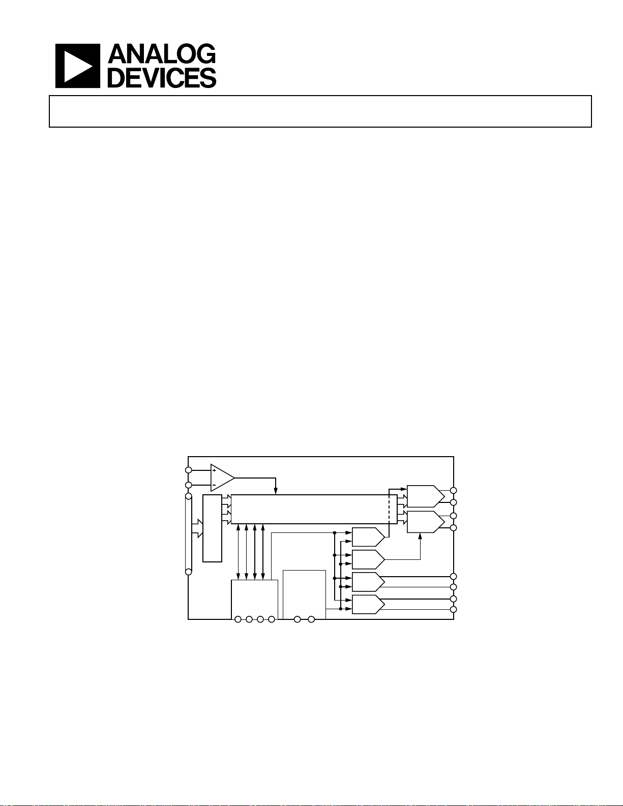
FUNCTIONAL BLOCK DIAGRAM
CLKP
CLKN
LVDS
INTERFACE
D[15:0]
, V
V
IA
IB
DEINTERLEAVING
LOGIC
SERIAL
PERIPHERAL
INTERFACE
SDO
SDIO
SCLK
Rev. A
Information furnished by Analog Devices is believed to be accurate and reliable. However, no
responsibility is assumed by Analog Devices for its use, nor for any infringements of patents or other
rights of third parties that may result from its use. Specifications subject to change without notice. No
license is granted by implication or otherwise under any patent or patent rights of Analog Devices.
Trademarks and registered trademarks are the property of their respective owners.
AD9783 DUAL LVDS DAC
INTERFACE LOGIC
INTERNAL
REFERENCE
AND
BIAS
CSB
REFIO
Figure 1.
16-BIT
I DAC
16-BIT
GAIN
DAC
GAIN
DAC
OFFSET
DAC
OFFSET
DAC
RESET
One Technology Way, P.O. Box 9106, Norwood, MA 02062-9106, U.S.A.
Tel: 781.329.4700 www.analog.com
Fax: 781.461.3113 ©2007–2008 Analog Devices, Inc. All rights reserved.
Q DAC
IOUT1P
IOUT1N
IOUT2P
IOUT2N
AUX1P
AUX1N
AUX2P
AUX2N
06936-001
Page 2

AD9780/AD9781/AD9783
TABLE OF CONTENTS
Features .............................................................................................. 1
Applications ....................................................................................... 1
General Description ......................................................................... 1
Product Highlights ........................................................................... 1
Functional Block Diagram .............................................................. 1
Revision History ............................................................................... 2
Specifications ..................................................................................... 3
DC Specifications ......................................................................... 3
Digital Specifications ................................................................... 4
AC Specifications .......................................................................... 4
Absolute Maximum Ratings ............................................................ 5
Thermal Resistance ...................................................................... 5
ESD Caution .................................................................................. 5
Pin Configurations and Function Descriptions ........................... 6
Typical Performance Characteristics ............................................. 9
Terminology .................................................................................... 17
Theory of Operation ...................................................................... 18
Serial Peripheral Interface ......................................................... 18
General Operation of the Serial Interface ............................... 18
Instruction Byte .......................................................................... 18
MSB/LSB Transfers .................................................................... 19
Serial Interface Port Pin Descriptions ..................................... 19
SPI Register Map ............................................................................ 20
SPI Register Descriptions .............................................................. 21
SPI Port, RESET, and Pin Mode ............................................... 23
Parallel Data Port Interface ........................................................... 24
Optimizing the Parallel Port Timing ....................................... 24
Driving the CLK Input .............................................................. 26
Full-Scale Current Generation ................................................. 26
DAC Transfer Function ............................................................. 27
Analog Modes of Operation ..................................................... 27
Power Dissipation....................................................................... 29
Evaluation Board Schematics ........................................................ 30
Outline Dimensions ....................................................................... 35
Ordering Guide .......................................................................... 35
REVISION HISTORY
6/08—Rev. 0 to Rev. A
Changed Maximum Sample Rate to 500 MHz Throughout ....... 1
Changes to Table 3 ............................................................................ 4
Changes to Building the Array Section ....................................... 25
Changes to Determining the SMP Value Section ....................... 25
Added Evaluation Board Schematics Section ............................. 30
Updated Outline Dimensions ....................................................... 35
11/07—Revision 0: Initial Version
Rev. A | Page 2 of 36
Page 3
AD9780/AD9781/AD9783
SPECIFICATIONS
DC SPECIFICATIONS
T
to T
MIN
otherwise noted.
Table 1.
AD9780 AD9781 AD9783
Parameter Min Typ Max Min Typ Max Min Typ Max Unit
RESOLUTION 12 14 16 Bits
ACCURACY
Differential Nonlinearity (DNL) ±0.13 ±0.5 ±2 LSB
Integral Nonlinearity (INL) ±0.25 ±1 ±4 LSB
MAIN DAC OUTPUTS
Offset Error –0.001 0 +0.001 –0.001 0 +0.001 –0.001 0 +0.001 % FSR
Gain Error (with Internal Reference) ±2 ±2 ±2 % FSR
Full-Scale Output Current
Output Compliance Range –1.0 +1.0 –1.0 +1.0 –1.0 +1.0 V
Output Resistance 10 10 10 MΩ
Main DAC Monotonicity Guaranteed
MAIN DAC TEMPERATURE DRIFT
Offset 0.04 0.04 0.04 ppm/°C
Gain 100 100 100 ppm/°C
Reference Voltage 30 30 30 ppm/°C
AUX DAC OUTPUTS
Resolution 10 10 10 Bits
Full-Scale Output Current –2 +2 –2 +2 –2 +2 mA
Output Compliance Range (Source) 0 1.6 0 1.6 0 1.6 V
Output Compliance Range (Sink) 0.8 1.6 0.8 1.6 0.8 1.6 V
Output Resistance 1 1 1 MΩ
AUX DAC Monotonicity Guaranteed
REFERENCE
Internal Reference Voltage 1.2 1.2 1.2 V
Output Resistance 5 5 5 kΩ
ANALOG SUPPLY VOLTAGES
AVDD33 3.13 3.3 3.47 3.13 3.3 3.47 3.13 3.3 3.47 V
CVDD18 1.70 1.8 1.90 1.70 1.8 1.90 1.70 1.8 1.90 V
DIGITAL SUPPLY VOLTAGES
DVDD33 3.13 3.3 3.47 3.13 3.3 3.47 3.13 3.3 3.47 V
DVDD18 1.70 1.8 1.90 1.70 1.8 1.90 1.70 1.8 1.90 V
POWER CONSUMPTION
f
DAC
f
DAC
Power-Down Mode 3 5 3 5 3 35 mW
SUPPLY CURRENTS
AVDD33 55 58 55 58 55 58 mA
CVDD18 34 38 34 38 34 38 mA
DVDD33 13 15 13 15 13 15 mA
DVDD18 68 85 68 85 68 85 mA
1
Based on a 10 kΩ external resistor.
2
f
= 500 MSPS, f
DAC
, AVDD33 = 3.3 V, DVDD33 = 3.3 V, DVDD18 = 1.8 V, CVDD18 = 1.8 V, I
MAX
1
8.66 20.2 31.66 8.66 20.2 31.66 8.66 20.2 31.66 mA
= 20 mA maximum sample rate, unless
OUTFS
= 500 MSPS, IF = 20 MHz V × I V × I V × I V × I V × I V × I mW
= 500 MSPS, IF = 10 MHz 440 440 440 mW
2
= 20 MHz.
OUT
Rev. A | Page 3 of 36
Page 4
AD9780/AD9781/AD9783
DIGITAL SPECIFICATIONS
T
to T
MIN
, AVDD33 = 3.3 V, DVDD33 = 3.3 V, DVDD18 = 1.8 V, CVDD18 = 1.8 V, I
MAX
otherwise noted.
Table 2.
Parameter Min Typ Max Unit
DAC CLOCK INPUT (CLKP, CLKN)
Peak-to-Peak Voltage at CLKP and CLKN 400 800 1600 mV
Common-Mode Voltage 300 400 500 mV
Maximum Clock Rate 500 MSPS
SERIAL PERIPHERAL INTERFACE (CMOS INTERFACE)
Maximum Clock Rate (SCLK) 40 MHz
Minimum Pulse Width High 12.5 ns
Minimum Pulse Width Low 12.5 ns
DIGITAL INPUT DATA (LVDS INTERFACE)
Input Voltage Range, VIA or VIB 800 1600 mV
Input Differential Threshold, V
Input Differential Hysteresis, V
−100 +100 mV
IDTH
IDTHH
to V
20 mV
IDTHL
Input Differential Input Impedance, RIN 80 120 Ω
Maximum LVDS Input Rate (per DAC) 500 MSPS
= 20 mA maximum sample rate, unless
OUTFS
AC SPECIFICATIONS
T
to T
MIN
otherwise noted.
Table 3.
Parameter
SPURIOUS FREE DYNAMIC RANGE (SFDR)
f
DAC
f
DAC
f
DAC
f
DAC
TWO-TONE INTERMODULATION DISTORTION (IMD)
f
DAC
f
DAC
f
DAC
f
DAC
ONE-TONE NOISE SPECTRAL DENSITY (NSD)
f
DAC
f
DAC
f
DAC
f
DAC
W-CDMA ADJACENT CHANNEL LEAKAGE RATIO (ACLR),
SINGLE CARRIER
f
DAC
f
DAC
f
DAC
f
DAC
, AVDD33 = 3.3 V, DVDD33 = 3.3 V, DVDD18 = 1.8 V, CVDD18 = 1.8 V, I
MAX
AD9780 AD9781 AD9783
= 500 MSPS, f
= 500 MSPS, f
= 500 MSPS, f
= 500 MSPS, f
= 500 MSPS, f
= 500 MSPS, f
= 500 MSPS, f
= 500 MSPS, f
= 500 MSPS, f
= 500 MSPS, f
= 500 MSPS, f
= 500 MSPS, f
= 20 MHz 79 78 80 dBc
OUT
= 120 MHz 67 66 68 dBc
OUT
= 380 MHz (Mix Mode) 55 58 62 dBc
OUT
= 480 MHz (Mix Mode) 58 62 59 dBc
OUT
= 20 MHz 91 93 86 dBc
OUT
= 120 MHz 80 75 79 dBc
OUT
= 380 MHz (Mix Mode) 69 70 64 dBc
OUT
= 480 MHz (Mix Mode) 60.5 61.5 66 dBc
OUT
= 40 MHz −157 −162 −165 dBc
OUT
= 120 MHz −154.5 −156.5 −157 dBc
OUT
= 380 MHz (Mix Mode) −153 −153 −154 dBc
OUT
= 480 MHz (Mix Mode) −152 −152 −153 dBc
OUT
= 491.52 MSPS, f
= 491.52 MSPS, f
= 491.52 MSPS, f
= 491.52 MSPS, f
= 20 MHz −81 −82.5 −82 dBc
OUT
= 80 MHz −80 −82.5 −81 dBc
OUT
= 411.52 MHz −71 −68 −69 dBc
OUT
= 471.52 MHz −69 −69 −70 dBc
OUT
= 20 mA, maximum sample rate, unless
OUTFS
Unit Min Typ Max Min Typ Max Min Typ Max
Rev. A | Page 4 of 36
Page 5
AD9780/AD9781/AD9783
ABSOLUTE MAXIMUM RATINGS
Table 4.
With
Parameter
AVDD33, DVDD33 AGND, DGND, CGND −0.3 V to +3.6 V
DVDD18, CVDD18 AGND, DGND, CGND −0.3 V to +1.98 V
AGND DGND, CGND −0.3 V to +0.3 V
DGND AGND, CGND −0.3 V to +0.3 V
CGND AGND, DGND −0.3 V to +0.3 V
REFIO AGND
IOUT1P, IOUT1N,
IOUT2P, IOUT2N,
AUX1P, AUX1N,
AUX2P, AUX2N
D15 to D0 DGND
CLKP, CLKN CGND
CSB, SCLK, SDIO, SDO DGND
Junction Temperature +125°C
Storage Temperature −65°C to +150°C
Respect to
AGND
Rating
−0.3 V to
AVDD33 + 0.3 V
−1.0 V to
AVDD33 + 0.3 V
−0.3 V to
DVDD33 + 0.3 V
−0.3 V to
CVDD18 + 0.3 V
–0.3 V to
DVDD33 + 0.3 V
THERMAL RESISTANCE
Thermal resistance is tested using a JEDEC standard 4-layer
thermal test board with no airflow.
Table 5.
Package Type θJA Unit
CP-72-1 (Exposed Pad Soldered to PCB) 25 °C/W
Stresses above those listed under Absolute Maximum Ratings
may cause permanent damage to the device. This is a stress
rating only; functional operation of the device at these or any
other conditions above those indicated in the operational
section of this specification is not implied. Exposure to absolute
maximum rating conditions for extended periods may affect
device reliability.
ESD CAUTION
Rev. A | Page 5 of 36
Page 6
AD9780/AD9781/AD9783
PIN CONFIGURATIONS AND FUNCTION DESCRIPTIONS
AVD D33
AVD D33
AVS S
IOUT1P
IOUT1N
AVS S
AUX1P
AUX1N
AVS S
AUX2N
AUX2P
AVS S
IOUT2N
IOUT2P
AVS S
AVD D33
AVD D33
REFIO
7271706968676665646362616059585756
1
CVDD18
2
CVSS
3
CLKP
4
CLKN
5
CVSS
6
CVDD18
7
DVSS
8
DVDD18
9
D11P
10
D11N
11
D10P
12
D10N
13
D9P
14
D9N
15
D8P
16
D8N
17D7P
18D7N
NOTES
1. NC = NO CO NNECT
2. EXPOSED PAD MUST BE
SOLDERED TO PCB AND
CONNECTED TO AVSS.
PIN 1
INDICATOR
192021222324252627282930313233
D6P
D5P
D6N
Figure 2. AD9780 Pin Configuration
D5N
D4P
D4N
AD9780
(TOP VIEW)
DVSS
DCOP
DCON
DVDD33
D3P
DCIP
DCIN
55
54
FS ADJ
53
RESET
52
CSB
51
SCLK
50
SDIO
49
SDO
48
DVSS
47
DVDD18
46
NC
45
NC
44
NC
43
NC
42
NC
41
NC
40
NC
39
NC
38
D0N
37
D0P
35D1P
36D1N
34
D2P
D3N
D2N
06936-002
Table 6. AD9780 Pin Function Descriptions
Pin No. Mnemonic Description
1, 6 CVDD18 Clock Supply Voltage (1.8 V).
2, 5 CVSS Clock Supply Return.
3, 4 CLKP, CLKN Differential DAC Sampling Clock Input.
7, 28, 48 DVSS Digital Common.
8, 47 DVDD18 Digital Supply Voltage (1.8 V).
9 to 24, 31 to 38 D11P, D11N to D0P, D0N LVDS Data Inputs. D11 is the MSB, D0 is the LSB.
25, 26 DCOP, DCON Differential Data Clock Output. LVDS clock at the DAC sample rate.
27 DVDD33 Digital Input and Output Pad Ring Supply Voltage (3.3 V).
29, 30 DCIP, DCIN Differential Data Clock Input. LVDS clock aligned with input data.
39 to 46 NC No Connection. Leave these pins floating.
49 SDO Serial Port Data Output.
50 SDIO Serial Port Data Input (4-Wire Mode) or Bidirectional Serial Data Line (3-Wire Mode).
51 SCLK Serial Port Clock Input.
52 CSB Serial Port Chip Select (Active Low).
53 RESET Chip Reset (Active High).
54 FS ADJ Full-Scale Current Output Adjust.
55 REFIO Analog Reference Input/Output (1.2 V Nominal).
56, 57, 71, 72 AVDD33 Analog Supply Voltage (3.3 V).
58, 61, 64, 67, 70 AVSS Analog Common.
59 IOUT2P DAC Current Output. Full-scale current is sourced when all data bits are 1s.
60 IOUT2N Complementary DAC Current Output. Full-scale current is sourced when all data bits are 0s.
62, 63 AUX2P, AUX2N Differential Auxiliary DAC Current Output (Channel 2).
65, 66 AUX1N, AUX1P Differential Auxiliary DAC Current Output (Channel 1).
68 IOUT1N Complementary DAC Current Output. Full-scale current is sourced when all data bits are 0s.
69 IOUT1P DAC Current Output. Full-scale current is sourced when all data bits are 1s.
Heat Sink Pad N/A The heat sink pad on the bottom of the package should be soldered to the PCB plane that
carries AVSS.
Rev. A | Page 6 of 36
Page 7
AD9780/AD9781/AD9783
AVDD33
AVDD33
AVSS
IOUT1P
IOUT1N
AVSS
AUX1P
AUX1N
AVSS
AUX2N
AUX2P
AVSS
IOUT2N
IOUT2P
AVSS
AVDD33
AVDD33
REFIO
7271706968676665646362616059585756
55
CVDD18
CVDD18
DVDD18
NOTES
1. NC = NO CONNECT
2. EXPOSED PAD MUST BE
SOLDERED TO PCB AND
CONNECTED TO AVSS.
CVSS
CLKP
CLKN
CVSS
DVSS
D13P
D13N
D12P
D12N
D11P
D11N
D10P
D10N
1
2
3
4
5
6
7
8
9
10
11
12
13
14
15
16
17D9P
18D9N
PIN 1
INDICATOR
(TOP VIEW)
192021222324252627282930313233
D8P
D7P
D6P
D8N
D7N
D6N
DCOP
AD9781
DCON
DVDD33
FS ADJ
54
RESET
53
CSB
52
SCLK
51
SDIO
50
SDO
49
DVSS
48
DVDD18
47
NC
46
NC
45
NC
44
NC
43
D0N
42
D0P
41
D1N
40
D1P
39
D2N
38
D2P
37
34
35D3P
36D3N
D5P
D4P
D5N
DCIP
DVSS
D4N
DCIN
06936-003
Figure 3. AD9781 Pin Configuration
Table 7. AD9781 Pin Function Descriptions
Pin No. Mnemonic Description
1, 6 CVDD18 Clock Supply Voltage (1.8 V).
2, 5 CVSS Clock Supply Return.
3, 4 CLKP, CLKN Differential DAC Sampling Clock Input.
7, 28, 48 DVSS Digital Common.
8, 47 DVDD18 Digital Supply Voltage (1.8 V).
9 to 24, 31 to 42 D13P, D13N to D0P, D0N LVDS Data Inputs. D13 is the MSB, D0 is the LSB.
25, 26 DCOP, DCON Differential Data Clock Output. LVDS clock at the DAC sample rate.
27 DVDD33 Digital Input and Output Pad Ring Supply Voltage (3.3 V).
29, 30 DCIP, DCIN Differential Data Clock Input. LVDS clock aligned with input data.
43 to 46 NC No Connection. Leave these pins floating.
49 SDO Serial Port Data Output.
50 SDIO Serial Port Data Input (4-Wire Mode) or Bidirectional Serial Data Line (3-Wire Mode).
51 SCLK Serial Port Clock Input.
52 CSB Serial Port Chip Select (Active Low).
53 RESET Chip Reset (Active High).
54 FS ADJ Full-Scale Current Output Adjust.
55 REFIO Analog Reference Input/Output (1.2 V Nominal).
56, 57, 71, 72 AVDD33 Analog Supply Voltage (3.3 V).
58, 61, 64, 67, 70 AVSS Analog Common.
59 IOUT2P DAC Current Output. Full-scale current is sourced when all data bits are 1s.
60 IOUT2N Complementary DAC Current Output. Full-scale current is sourced when all data bits are 0s.
62, 63 AUX2P, AUX2N Differential Auxiliary DAC Current Output (Channel 2).
65, 66 AUX1N, AUX1P Differential Auxiliary DAC Current Output (Channel 1).
68 IOUT1N Complementary DAC Current Output. Full-scale current is sourced when all data bits are 0s.
69 IOUT1P DAC Current Output. Full-scale current is sourced when all data bits are 1s.
Heat Sink Pad N/A
The heat sink pad on the bottom of the package should be soldered to the PCB plane that
carries AVSS.
Rev. A | Page 7 of 36
Page 8
AD9780/AD9781/AD9783
AVDD33
AVDD33
AVSS
IOUT1P
IOUT1N
AVSS
AUX1P
AUX1N
AVSS
AUX2N
AUX2P
AVSS
IOUT2N
IOUT2P
AVSS
AVDD33
AVDD33
REFIO
7271706968676665646362616059585756
55
CVDD18
CVDD18
DVDD18
NOTES
1. EXPOSED PAD MUST BE
SOLDERED TO PCB AND
CONNECTED TO AVSS.
CVSS
CLKP
CLKN
CVSS
DVSS
D15P
D15N
D14P
D14N
D13P
D13N
D12P
D12N
1
2
3
4
5
6
7
8
9
10
11
12
13
14
15
16
17D11P
18D11N
PIN 1
INDICATOR
(TOP VIEW)
192021222324252627282930313233
D9P
D8P
D9N
D10P
D8N
D10N
AD9783
DCOP
DCON
DVDD33
FS ADJ
54
RESET
53
CSB
52
SCLK
51
SDIO
50
SDO
49
DVSS
48
DVDD18
47
D0N
46
D0P
45
D1N
44
D1P
43
D2N
42
D2P
41
D3N
40
D3P
39
D4N
38
D4P
37
34
35D5P
36D5N
D7P
D6P
D7N
DCIP
DVSS
D6N
DCIN
06936-004
Figure 4. AD9783 Pin Configuration
Table 8. AD9783 Pin Function Descriptions
Pin No. Mnemonic Description
1, 6 CVDD18 Clock Supply Voltage (1.8 V).
2, 5 CVSS Clock Supply Return.
3, 4 CLKP, CLKN Differential DAC Sampling Clock Input.
7, 28, 48 DVSS Digital Common.
8, 47 DVDD18 Digital Supply Voltage (1.8 V).
9 to 24, 31 to 46 D15P, D15N to D0P, D0N LVDS Data Inputs. D15 is the MSB, D0 is the LSB.
25, 26 DCOP, DCON Differential Data Clock Output. LVDS clock at the DAC sample rate.
27 DVDD33 Digital Input and Output Pad Ring Supply Voltage (3.3 V).
29, 30 DCIP, DCIN Differential Data Clock Input. LVDS clock aligned with input data.
49 SDO Serial Port Data Output.
50 SDIO Serial Port Data Input (4-Wire Mode) or Bidirectional Serial Data Line (3-Wire Mode).
51 SCLK Serial Port Clock Input.
52 CSB Serial Port Chip Select (Active Low).
53 RESET Chip Reset (Active High).
54 FS ADJ Full-Scale Current Output Adjust.
55 REFIO Analog Reference Input/Output (1.2 V Nominal).
56, 57, 71, 72 AVDD33 Analog Supply Voltage (3.3 V).
58, 61, 64, 67, 70 AVSS Analog Common.
59 IOUT2P DAC Current Output. Full-scale current is sourced when all data bits are 1s.
60 IOUT2N Complementary DAC Current Output. Full-scale current is sourced when all data bits are 0s.
62, 63 AUX2P, AUX2N Differential Auxiliary DAC Current Output (Channel 2).
65, 66 AUX1N, AUX1P Differential Auxiliary DAC Current Output (Channel 1).
68 IOUT1N Complementary DAC Current Output. Full-scale current is sourced when all data bits are 0s.
69 IOUT1P DAC Current Output. Full-scale current is sourced when all data bits are 1s.
Heat Sink Pad N/A
The heat sink pad on the bottom of the package should be soldered to the PCB plane that
carries AVSS.
Rev. A | Page 8 of 36
Page 9
AD9780/AD9781/AD9783
TYPICAL PERFORMANCE CHARACTERISTICS
1.5
1.0
0.5
0
–0.5
LSB
–1.0
–1.5
–2.0
–2.5
0 32,76816,384 65,535
CODE
49,152
Figure 5. AD9783 INL, TA = 85°C, FS = 20 mA
06936-005
0.4
0.2
0
–0.2
–0.4
–0.6
LSB
–0.8
–1.0
–1.2
–1.4
–1.6
0
32,76816,384 65,53549,152
CODE
06936-008
Figure 8. AD9783 DNL, TA = 85°C, FS = 20 mA
5
4
3
2
1
LSB
0
–1
–2
–3
0
32,76816,384 65,53549,152
CODE
06936-006
Figure 6. AD9783 INL, TA = 25°C, FS = 20 mA
5
4
3
2
1
LSB
0
–1
–2
–3
0
32,76816,384 65,53549,152
CODE
06936-007
Figure 7. AD9783 INL, TA = −40°C, FS = 20 mA
0.4
0.2
0
–0.2
–0.4
–0.6
LSB
–0.8
–1.0
–1.2
–1.4
–1.6
0
32,76816,384 65,53549,152
CODE
Figure 9. AD9783 DNL, TA = 25°C, FS = 20 mA
1.0
0.8
0.6
0.4
0.2
0
LSB
–0.2
–0.4
–0.6
–0.8
–1.0
0
32,76816,384 65,53549,152
CODE
Figure 10. AD9783 DNL, TA = −40°C, FS = 20 mA
06936-009
06936-010
Rev. A | Page 9 of 36
Page 10
AD9780/AD9781/AD9783
0.4
0.3
0.2
0.1
0
–0.1
LSB
–0.2
–0.3
–0.4
–0.5
–0.6
40960 8192 12,288 16, 383
CODE
06936-011
Figure 11. AD9781 INL, TA = 85°C, FS = 20 mA
0.059
–0.060
–0.179
LSB
–0.297
–0.416
40960 8192 12,288 16, 383
CODE
Figure 14. AD9781 DNL, TA = 85°C, FS = 20 mA
06936-014
0.6
0.4
0.2
0
–0.2
LSB
–0.4
–0.6
–0.8
–1.0
0 4096 8192 12288 16,383
CODE
Figure 12. AD9781 INL, TA = −40°C, FS = 20 mA
0.2
0.1
0
–0.1
–0.2
LSB
–0.3
–0.4
0.1
0
–0.1
–0.2
LSB
–0.3
–0.4
–0.5
0 16,383
06936-012
4096 8192 12,288
CODE
06936-015
Figure 15. AD9781 DNL, TA = −40°C, FS = 20 mA
0.2
0.1
0
–0.1
–0.2
LSB
–0.3
–0.4
–0.5
–0.6
0 1024 2048 3072 4096
CODE
Figure 13. AD9780 INL, TA = −40°C, FS = 20 mA
06936-013
Rev. A | Page 10 of 36
–0.5
–0.6
0
1024 2048 3072 4096
CODE
Figure 16. AD9780 INL, TA = 85°C, FS = 20 mA
06936-016
Page 11
AD9780/AD9781/AD9783
90
85
80
75
70
65
60
SFDR (dBc)
55
50
45
40
0 50 100 150 200 250 300 350 400 450 500
250MSPS
Figure 17. AD9783 SFDR vs. f
100
95
90
85
80
75
70
65
SFDR (dBc)
60
55
50
45
40
0 25 50 75 100 125 150 175 200 225 250
Figure 18. AD9783 SFDR vs. f
400MSPS
500MSPS
f
(MHz)
OUT
Over f
OUT
in Baseband and Mix Modes,
DAC
FS = 20 mA
20mA
30mA
10mA
f
(MHz)
OUT
Over Analog Output, TA = 25°C, at 500 MSPS
OUT
100
95
90
85
80
75
70
65
SFDR (dBc)
60
55
50
45
40
0 25 50 75 100 125 150 175 200 225 250
06936-017
Figure 20. AD9783 SFDR vs. f
100
95
90
85
80
75
70
400MSPS
IMD (dBc)
65
60
55
50
45
8
1
0
6
3
9
6
0
40
0 50 100 150 200 500250 300 350 40 0 450
Figure 21. AD9783 IMD vs. f
+85°C
+25°C
–40°C
f
(MHz)
OUT
Over Temperature, at 500 MSPS, FS = 20 mA
OUT
250MSPS
500MSPS
f
(MHz)
OUT
Over f
OUT
in Baseband and Mix Modes,
DAC
06936-020
06936-021
FS = 20 mA
100
95
90
85
80
75
70
65
–6dBFS
SFDR (dBc)
60
55
50
45
40
0 25 50 75 100 125 150 175 200 225 250
Figure 19. AD9783 SFDR vs. f
T
–3dBFS
0dBFS
f
(MHz)
OUT
Over Digital Input Level,
= 25°C, at 500 MSPS, FS = 20 mA
A
OUT
06936-019
Figure 22. AD9783 IMD vs. f
Rev. A | Page 11 of 36
100
95
90
85
80
75
70
IMD (dBc)
65
60
55
50
45
40
0 25 50 75 100 125 150 175 200 225 250
30mA
10mA
20mA
f
(MHz)
OUT
Over Analog Output, TA = 25°C, at 500 MSPS
OUT
06936-022
Page 12

AD9780/AD9781/AD9783
–
–
–
–
100
95
90
85
80
75
70
65
IMD (dBc)
60
55
50
45
40
0 30 60 90 120 150 180 210 240
Figure 23. AD9783 IMD vs. f
–6dBFS
–3dBFS
0dBFS
f
(MHz)
OUT
Over Digital Input Level, TA = 25°C, at
OUT
500 MSPS, FS = 20 mA
06936-023
140
–143
–146
–149
–152
–155
–158
NSD (dBm/Hz)
–161
–164
–167
–170
0 50 100 150 200 250 300 350 400 450 500
Figure 26. AD9783 Eight-Tone NSD vs. f
250MSPS
400MSPS
f
OUT
500MSPS
(MHz)
OUT
Over f
DAC
Mix Modes, FS = 20 mA
06936-026
Baseband and
100
95
90
85
80
75
70
IMD (dBc)
65
60
55
50
45
40
0 30 60 90 120 150 180 210 240
Figure 24. AD9783 IMD vs. f
140
–143
–146
–149
–152
500MSPS
–155
–158
NSD (dBm/Hz)
–161
–164
–167
–170
0 50 100 150 200 250 300 350 400 450 500
+85°C
–40°C
Over Temperature, at 500 MSPS, FS = 20 mA
OUT
250MSPS
400MSPS
Figure 25. AD9783 One-Tone NSD vs. f
FS = 20 mA
f
OUT
f
OUT
OUT
(MHz)
(MHz)
Over f
+25°C
Baseband and Mix Modes,
DAC
140
–143
–146
–149
–152
–155
–158
NSD (dBm/Hz)
–161
–164
–167
–170
0255075
06936-024
Figure 27. AD9783 One-Tone NSD vs. f
125 150 175
100
f
OUT
(MHz)
OUT
+85°C
+25°C
–40°C
225 25 0
200
Over Temperature, at 500 MSPS,
06936-027
FS = 20 mA
140
–143
–146
–149
–152
–155
–158
NSD (dBm/Hz)
–161
–164
–167
–170
0255075
06936-025
Figure 28. AD9783 Eight-Tone NSD vs. f
+85°C
–40°C
125 150 175
100
f
OUT
+25°C
225 25 0
(MHz)
Over Temperature, at 500 MSPS,
OUT
200
06936-028
FS = 20 mA
Rev. A | Page 12 of 36
Page 13

AD9780/AD9781/AD9783
–
–
–
–
–
–
50
50
–55
–60
491.52MSPS
ACLR (dBc)
–65
–70
–75
–80
–85
–90
0 500400300200100
245.76MSPS
f
(MHz)
OUT
Figure 29. AD9783 ACLR for First Adjacent Band One-Carrier W-CDMA
Baseband and Mix Modes, FS = 20 mA
50
–55
–60
–65
–70
ACLR (dBc)
–75
245.76MSPS
491.52MSPS
–55
–60
–65
–70
ACLR (dBc)
–75
–80
–85
–90
0 500400300200100
06936-029
0dB
–3dB
f
(MHz)
OUT
6936-032
Figure 32. AD9783 ACLR for First Adjacent Channel Two-Carrier W-CDMA
Over Digital Input Level Baseband and Mix Modes, at 491.52 MSPS,
FS = 20 mA
50
–55
–60
–65
–70
ACLR (dBc)
–75
–3dB
–80
–85
–90
0 500400300200100
f
(MHz)
OUT
Figure 30. AD9783 ACLR for Second Adjacent Band One-Carrier W-CDMA
Baseband and Mix Modes, FS = 20 mA
50
–55
–60
–65
245.76MSPS
f
(MHz)
OUT
491.52MSPS
ACLR (dBc)
–70
–75
–80
–85
–90
0 500400300200100
Figure 31. AD9783 ACLR for Third Adjacent Band One-Carrier W-CDMA
Baseband and Mix Modes, FS = 20 mA
–80
–85
–90
0 500400300200100
06936-030
0dB
f
OUT
(MHz)
06936-033
Figure 33. AD9783 ACLR for Second Adjacent Channel Two-Carrier W-CDMA
Over Digital Input Level Baseband and Mix Modes, at 491.52 MSPS,
FS = 20 mA
50
–55
–60
–65
–70
ACLR (dBc)
–75
–80
–85
–90
0 500400300200100
06936-031
–3dB
0dB
06936-034
f
(MHz)
OUT
Figure 34. AD9783 ACLR for Third Adjacent Channel Two-Carrier W-CDMA
Over Digital Input Level Baseband and Mix Modes, at 491.52 MSPS,
FS = 20 mA
Rev. A | Page 13 of 36
Page 14
AD9780/AD9781/AD9783
–
–
–
50
–55
–60
–65
–70
ACLR (dB c)
–75
–80
–85
–90
0 500400300200100
0dB
–3dB
f
OUT
(MHz)
Figure 35. AD9783 ACLR for First Adjacent Channel Four-Carrier W-CDMA
Over Digital Input Level Baseband and Mix Modes, at 491.52 MSPS,
FS = 20 mA
50
06936-035
1.0
0.5
0
–0.5
–1.0
–1.5
–2.0
–2.5
–3.0
AMPLITUDE ( dBm)
–3.5
–4.0
–4.5
–5.0
0 600540480420360240 30018060 120
NORMAL MODE
f
(MHz)
OUT
MIX MODE
06936-038
Figure 38. Nominal Power in the Fundamental, FS = 20 mA, at 500 MSPS,
FS = 20 mA
0.8
–55
–60
–65
–70
ACLR (dB c)
–75
–80
–85
–90
–3dB
0 500400300200100
0dB
f
(MHz)
OUT
06936-036
Figure 36. AD9783 ACLR for Second Adjacent Channel Four-Carrier W-CDMA
Over Digital Input Level Baseband and Mix Modes, at 491.52 MSPS,
FS = 20 mA
50
–55
–60
–65
–70
ACLR (dBc)
–75
–80
–85
–90
0 500400300200100
–3dB
0dB
f
(MHz)
OUT
06936-037
Figure 37. AD9783 ACLR for Third Adjacent Channel Four-Carrier W-CDMA
Over Digital Input Level Baseband and Mix Modes, at 491.52 MSPS,
FS = 20 mA
0.6
0.4
0.2
0
LSB
–0.2
–0.4
–0.6
–0.8
0
4096 8192
CODE
12,288 16,383
06936-039
Figure 39. AD9781 INL, FS = 20 mA
0.1
0
–0.1
–0.2
LSB
–0.3
–0.4
–0.5
0
4096 8192
CODE
12,288 16, 383
06936-040
Figure 40. AD9781 DNL, FS = 20 mA
Rev. A | Page 14 of 36
Page 15
AD9780/AD9781/AD9783
–
–
100
95
90
85
80
75
70
65
SFDR (dBc)
60
55
50
45
40
0 50 100 150 200 500250 300 350 400 450
Figure 41. AD9781 SFDR vs. f
f
(MHz)
OUT
in Baseband and Mix Modes, at 500 MSPS,
OUT
FS = 20 mA
06936-041
50
–55
ACLR (dBc)
–60
–65
–70
–75
–80
–85
–90
0 500400300200100
FIRST
ADJACENT
CHANNEL
f
OUT
SECOND
ADJACENT
CHANNEL
(MHz)
THIRD
ADJACENT
CHANNEL
6936-044
Figure 44. AD9781 ACLR for One-Carrier W-CDMA Baseband and Mix Modes,
at 491.52 MSPS, FS = 20 mA
100
IMD @ 500MSPS
95
90
85
80
75
70
IMD (dBc)
65
60
55
50
45
40
0 60 120 180 240 600300 360 420 480 540
Figure 42. AD9781 IMD vs. f
f
(MHz)
OUT
in Baseband and Mix Modes, at 500 MSPS,
OUT
FS = 20 mA
140
–142
–144
–146
–148
–150
–152
–154
–156
–158
NSD (dBm/Hz)
–160
–162
–164
–166
–168
–170
0 50 100 150 200 500250 300 350 400 450
1-TONE
8-TONE
f
OUT
(MHz)
Figure 43. AD9781 One-Tone, Eight-Tone NSD vs. f
Modes, at 500 MSPS, FS = 20 mA
in Baseband and Mix
OUT
0.2
0.1
0
–0.1
–0.2
LSB
–0.3
–0.4
–0.5
–0.6
0
06936-042
1024 2048
CODE
3072 4096
06936-045
Figure 45. AD9780 INL, FS = 20 mA
0.04
0.02
0
–0.02
–0.04
LSB
–0.06
–0.08
–0.10
–0.12
0
06936-043
1024 2048
CODE
3072 4096
06936-046
Figure 46. AD9780 DNL, FS = 20 mA
Rev. A | Page 15 of 36
Page 16
AD9780/AD9781/AD9783
–
–
100
95
90
85
80
75
70
65
SFDR (dBc)
60
55
50
45
40
0 50 100 150 200 500250 300 350 400 450
Figure 47. AD9780 SFDR vs. f
f
(MHz)
OUT
in Baseband and Mix Modes, at 500 MSPS,
OUT
FS = 20 mA
06936-047
140
–142
–144
–146
–148
–150
–152
–154
–156
–158
NSD (dBm/Hz)
–160
–162
–164
–166
–168
–170
0 50 100 150 200 500250 300 350 400 450
1-TONE
8-TONE
f
OUT
(MHz)
Figure 49. AD9780 One-Tone, Eight-Tone NSD vs. f
Modes, at 500 MSPS, FS = 20 mA
in Baseband and Mix
OUT
06936-049
100
95
90
85
80
75
70
65
60
IMD (dBc)
55
50
45
40
35
30
0 50 100 150 200 500250 300 350 400 450
Figure 48. AD9780 IMD vs. f
f
(MHz)
OUT
in Baseband and Mix Modes, at 500 MSPS,
OUT
FS = 20 mA
50
–55
–60
–65
–70
ACLR (dBc)
–75
–80
–85
–90
0 500400300200100
06936-048
FIRST
ADJACENT
CHANNEL
f
OUT
SECOND
ADJACENT
CHANNEL
(MHz)
THIRD
ADJACENT
CHANNEL
06936-050
Figure 50. AD9780 ACLR for One-Carrier W-CDMA Baseband and Mix Modes,
at 491.52 MSPS, FS = 20 mA
Rev. A | Page 16 of 36
Page 17

AD9780/AD9781/AD9783
TERMINOLOGY
Linearity Error or Integral Nonlinearity (INL)
Linearity error is defined as the maximum deviation of the
actual analog output from the ideal output, determined by a
straight line drawn from zero scale to full scale.
Differential Nonlinearity (DNL)
DNL is the measure of the variation in analog value, normalized
to full scale, associated with a 1 LSB change in digital input code.
Monotonicity
A DAC is monotonic if the output either increases or remains
constant as the digital input increases.
Offset Error
Offset error is the deviation of the output current from the ideal
of zero. For I
all 0s. For I
, 0 mA output is expected when the inputs are
OUTA
, 0 mA output is expected when all inputs are
OUTB
set to 1s.
Gain Error
Gain error is the difference between the actual and ideal output
span. The actual span is determined by the difference between
the output when all inputs are set to 1s and the output when all
inputs are set to 0s.
Output Compliance Range
Output compliance range is the range of allowable voltage at
the output of a current-output DAC. Operation beyond the
maximum compliance limits can cause either output stage
saturation or breakdown, resulting in nonlinear performance.
Temp er at u re D ri ft
Temperature drift is specified as the maximum change from
the ambient (25°C) value to the value at either T
MIN
or T
MAX
.
For offset and gain drift, the drift is reported in ppm of fullscale range (FSR) per degree Celsius. For reference drift, the
drift is reported in ppm per degree Celsius.
Power Supply Rejection
Power supply rejection is the maximum change in the full-scale
output as the supplies are varied from minimum to maximum
specified voltages.
Settling Time
Settling time is the time required for the output to reach and
remain within a specified error band around its final value,
measured from the start of the output transition.
Spurious-Free Dynamic Range (SFDR)
SFDR is the difference, in decibels, between the peak amplitude
of the output signal and the peak spurious signal between dc
and the frequency equal to half the input data rate.
Total Harmonic Distortion (THD)
THD is the ratio of the rms sum of the first six harmonic components to the rms value of the measured fundamental. It is
expressed as a percentage or in decibels.
Signal-to-Noise Ratio (SNR)
SNR is the ratio of the rms value of the measured output signal
to the rms sum of all other spectral components below the Nyquist
frequency, excluding the first six harmonics and dc. The value
for SNR is expressed in decibels.
Adjacent Channel Leakage Ratio (ACLR)
ACLR is the ratio in dBc between the measured power within a
channel relative to its adjacent channel.
Complex Image Rejection
In a traditional two-part upconversion, two images are created
around the second IF frequency. These images usually waste
transmitter power and system bandwidth. By placing the real
part of a second complex modulator in series with the first
complex modulator, either the upper or lower frequency image
near the second IF can be rejected.
Rev. A | Page 17 of 36
Page 18

AD9780/AD9781/AD9783
THEORY OF OPERATION
The AD9780/AD9781/AD9783 have a combination of features
that make them very attractive for wired and wireless communications systems. The dual DAC architecture facilitates easy
interface to common quadrature modulators when designing
single sideband transmitters. In addition, the speed and
performance of the devices allow wider bandwidths and more
carriers to be synthesized than in previously available products.
All features and options are software programmable through
the SPI port.
SERIAL PERIPHERAL INTERFACE
SDO
SDIO
SCLK
CSB
The serial peripheral interface (SPI) port is a flexible, synchronous serial communications port allowing easy interface to many
industry-standard microcontrollers and microprocessors. The
port is compatible with most synchronous transfer formats,
including both the Motorola SPI and Intel
The interface allows read and write access to all registers that
configure the AD9780/AD9781/AD9783. Single or multiple
byte transfers are supported as well as MSB-first or LSB-first
transfer formats. Serial data input/output can be accomplished
through a single bidirectional pin (SDIO) or through two
unidirectional pins (SDIO/SDO).
The serial port configuration is controlled by Register 0x00,
Bits[7:6]. It is important to note that any change made to the
serial port configuration occurs immediately upon writing to
the last bit of this byte. Therefore, it is possible with a multibyte
transfer to write to this register and change the configuration in
the middle of a communication cycle. Care must be taken to
compensate for the new configuration within the remaining
bytes of the current communication cycle.
Use of a single-byte transfer when changing the serial port
configuration is recommended to prevent unexpected device
behavior.
AD9783
SPI
PORT
Figure 51. SPI Port
6936-051
® SSR protocols.
The Phase 1 instruction byte defines whether the upcoming
data transfer is a read or write, the number of bytes in the data
transfer, and a reference register address for the first byte of the
data transfer. A logic high on the CSB pin followed by a logic
low resets the SPI port to its initial state and defines the start of
the instruction cycle. From this point, the next eight rising
SCLK edges define the eight bits of the instruction byte for the
current communication cycle.
The remaining SCLK edges are for Phase 2 of the communication
cycle, which is the data transfer between the serial port controller
and the system controller. Phase 2 can be a transfer of one, two,
three, or four data bytes as determined by the instruction byte.
Using multibyte transfers is usually preferred, although singlebyte data transfers are useful to reduce CPU overhead or when
only a single register access is required.
All serial port data is transferred to and from the device in
synchronization with the SCLK pin. Input data is always latched
on the rising edge of SCLK, whereas output data is always valid
after the falling edge of SCLK. Register contents change immediately upon writing to the last bit of each transfer byte.
Anytime synchronization is lost, the device has the ability to
asynchronously terminate an I/O operation whenever the CSB pin
is taken to logic high. Any unwritten register content data is lost
if the I/O operation is aborted. Taking CSB low then resets the
serial port controller and restarts the communication cycle.
INSTRUCTION BYTE
The instruction byte contains the information shown in Ta bl e 9.
Table 9.
MSB
B7 B6 B5 B4 B3 B2 B1 B0
R/W N1 N0 A4 A3 A2 A1 A0
Bit 7, R/W, determines whether a read or a write data transfer
occurs after the instruction byte write. Logic 1 indicates a read
operation. Logic 0 indicates a write operation.
Bits[6:5], N1 and N0, determine the number of bytes to be
transferred during the data transfer cycle. The bits decode as
shown in Tab l e 10 .
LSB
GENERAL OPERATION OF THE SERIAL INTERFACE
There are two phases to any communication cycle with the
AD9780/AD9781/AD9783: Phase 1 and Phase 2. Phase 1 is
the instruction cycle, which writes an instruction byte into
the device. This byte provides the serial port controller with
information regarding Phase 2 of the communication cycle:
the data transfer cycle.
Rev. A | Page 18 of 36
Table 10. Byte Transfer Count
N1 N0 Description
0 0 Transfer one byte
0 1 Transfer two bytes
1 0 Transfer three bytes
1 1 Transfer four bytes
Page 19

AD9780/AD9781/AD9783
Bits[4:0], A4, A3, A2, A1, and A0, determine which register is
accessed during the data transfer of the communication cycle.
For multibyte transfers, this address is a starting or ending
address depending on the current data transfer mode. For
MSB-first format, the specified address is an ending address
or the most significant address in the current cycle. Remaining
register addresses for multiple byte data transfers are generated
internally by the serial port controller by decrementing from
the specified address. For LSB-first format, the specified address
is a beginning address or the least significant address in the
current cycle. Remaining register addresses for multiple byte
data transfers are generated internally by the serial port
controller by incrementing from the specified address.
MSB/LSB TRANSFERS
The serial port can support both MSB-first and LSB-first data
formats. This functionality is controlled by Register 0x00, Bit 6.
The default is Logic 0, which is MSB-first format.
When using MSB-first format (LSBFIRST = 0), the instruction
and data bit must be written from MSB to LSB. Multibyte data
transfers in MSB-first format start with an instruction byte that
includes the register address of the most significant data byte.
Subsequent data bytes are loaded into sequentially lower address
locations. In MSB-first mode, the serial port internal address
generator decrements for each byte of the multibyte data
transfer.
When using LSB-first format (LSBFIRST = 1), the instruction
and data bit must be written from LSB to MSB. Multibyte data
transfers in LSB-first format start with an instruction byte that
includes the register address of the least significant data byte.
Subsequent data bytes are loaded into sequentially higher
address locations. In LSB-first mode, the serial port internal
address generator increments for each byte of the multibyte
data transfer.
Use of a single-byte transfer when changing the serial port data
format is recommended to prevent unexpected device behavior.
SERIAL INTERFACE PORT PIN DESCRIPTIONS
Chip Select Bar (CSB)
Active low input starts and gates a communication cycle. It
allows more than one device to be used on the same serial
communication lines. CSB must stay low during the entire
communication cycle. Incomplete data transfers are aborted
anytime the CSB pin goes high. SDO and SDIO pins go to a
high impedance state when this input is high.
Serial Clock (SCLK)
The serial clock pin is used to synchronize data to and from the
device and to run the internal state machines. The maximum
frequency of SCLK is 40 MHz. All data input is registered on
the rising edge of SCLK. All data is driven out on the falling
edge of SCLK.
Serial Port Data I/O (SDIO)
Data is always written into the device on this pin. However,
SDIO can also function as a bidirectional data output line. The
configuration of this pin is controlled by Register 0x00, Bit 7.
The default is Logic 0, which configures the SDIO pin as
unidirectional.
Serial Port Data Output (SDO)
Data is read from this pin for protocols that use separate lines
for transmitting and receiving data. The configuration of this
pin is controlled by Register 0x00, Bit 7. If this bit is set to a
Logic 1, the SDO pin does not output data and is set to a high
impedance state.
INSTRUCTIO N CYCLE DATA TRANSFER CYCLE
CSB
SCLK
SDIO
SDO
R/W N1 N0 A4 A3 A2 A1 A0 D7 D6ND5
D7 D6ND5
N
N
D00D10D20D3
0
D00D10D20D3
0
Figure 52. Serial Register Interface Timing Diagram, MSB First
INSTRUCTIO N CYCLE DATA TRANSFER CYCLE
CSB
SCLK
SDIO
SDO
A0 A1 A2 A3 A4 N0 N1 R/W D00D10D2
D00D10D2
0
0
D7ND6ND5ND4
N
D7ND6ND5ND4
N
Figure 53. Serial Register Interface Timing Diagram, LSB First
t
PWH
t
–1
f
SCLK
t
PWL
DH
INSTRUCTIO N BIT 6INSTRUCTIO N BIT 7
CSB
SCLK
SDIO
t
S
t
DS
Figure 54. Timing Diagram for SPI Write Register
CSB
SCLK
t
DV
SDIO
SDO
Figure 55. Timing Diagram for SPI Read Register
DATA BIT N – 1DATA BIT N
06936-052
6936-053
06936-054
06936-055
Rev. A | Page 19 of 36
Page 20
AD9780/AD9781/AD9783
SPI REGISTER MAP
Table 11.
Register Name Addr Default Bit 7 Bit 6 Bit 5 Bit 4 Bit 3 Bit 2 Bit 1 Bit 0
SPI Control 0x00 0x00 SDIO_DIR LSBFIRST RESET
Data Control 0x02 0x00 DATA INVDCO
Power-Down 0x03 0x00 PD_DCO PD_INPT PD_AUX2 PD_AUX1 PD_BIAS PD_CLK PD_DAC2 PD_DAC1
Setup and Hold 0x04 0x00 SET[3:0] HLD[3:0]
Timing Adjust 0x05 0x00 SAMP_DLY[4:0]
Seek 0x06 0x00 LVDS low LVDS high SEEK
Mix Mode 0x0A 0x00 DAC1MIX[1:0] DAC2MIX[1:0]
DAC1 FSC 0x0B 0xF9 DAC1FSC[7:0]
DAC1 FSC MSBs 0x0C 0x01 DAC1FSC[9:8]
AUXDAC1 0x0D 0x00 AUXDAC1[7:0]
AUXDAC1 MSB 0x0E 0x00 AUX1SGN AUX1DIR AUXDAC1[9:8]
DAC2 FSC 0x0F 0xF9 DAC2FSC[7:0]
DAC2 FSC MSBs 0x10 0x01 DAC2FSC[9:8]
AUXDAC2 0x11 0x00 AUXDAC2[7:0]
AUXDAC2 MSB 0x12 0x00 AUX2SGN AUX2DIR AUXDAC2[9:8]
BIST Control 0x1A 0x00 BISTEN BISTRD BISTCLR
BIST Result 1 Low 0x1B 0x00 BISTRES1[7:0]
BIST Result 1 High 0x1C 0x00 BISTRES1[15:8]
BIST Result 2 Low 0x1D 0x00 BISTRES2[7:0]
BIST Result 2 High 0x1E 0x00 BISTRES2[15:8]
Hardware Version 0x1F N/A VERSION[3:0] DEVICE[3:0]
Rev. A | Page 20 of 36
Page 21
AD9780/AD9781/AD9783
SPI REGISTER DESCRIPTIONS
Reading these registers returns previously written values for all defined register bits, unless otherwise noted.
Table 12.
Register Address Bit Name Function
SPI Control 0x00 7 SDIO_DIR 0, operate SPI in 4-wire mode. The SDIO pin operates as an input only pin.
1, operate SPI in 3-wire mode. The SDIO pin operates as a bidirectional data line.
6 LSBFIRST 0, MSB first per SPI standard.
1, LSB first per SPI standard.
5 RESET
1, set software reset, write 0 on the next (or any following) cycle to release the reset.
Data Control 0x02 7 DATA 0, DAC input data is twos complement binary format.
1, DAC input data is unsigned binary format.
4 INVDCO 1, inverts the data clock output. Used for adjusting timing of input data.
Power-Down 0x03 7 PD_DCO 1, power down data clock output driver circuit.
6 PD_INPT 1, power down input.
5 PD_AUX2 1, power down AUX2 DAC
4 PD_AUX1 1, power down AUX1 DAC.
3 PD_BIAS 1, power down voltage reference bias circuit.
2 PD_CLK 1, power down DAC clock input circuit.
1 PD_DAC2 1, power down DAC2.
0 PD_DAC1 1, power down DAC1.
Setup and Hold 0x04 7:4 SET[3:0] 4-bit value used to determine input data setup timing.
3:0 HLD[3:0] 4-bit value used to determine input data hold timing.
Timing Adjust 0x05 4:0 SAMP_DLY[4:0] 5-bit value used to optimally position input data relative to internal sampling clock.
Seek 0x06 2 LVDS low
1 LVDS high
0 SEEK
Mix Mode 0x0A 3:2 DAC1MIX[1:0] 00, selects normal mode, DAC1.
01, selects return-to-zero mode, DAC1.
10, selects return-to-zero mode, DAC1.
11, selects mix mode, DAC1.
1:0 DAC2MIX[1:0] 00, selects normal mode, DAC2.
01, selects return-to-zero mode, DAC2.
10, selects return-to-zero mode, DAC2.
11, selects mix mode, DAC2.
DAC1 FSC 0x0B 7:0 DAC1FSC[9:0] DAC1 full-scale 10-bit adjustment word.
0x0C 1:0 0x3FF, sets DAC full-scale output current to the maximum value of 31.66 mA.
0x200, sets DAC full-scale output current to the nominal value of 20.0 mA.
0x000, sets DAC full-scale output current to the minimum value of 8.66 mA.
Only change LSB/MSB order in single-byte instructions to avoid erratic behavior
due to bit order errors.
0, execute software reset of SPI and controllers, reload default register values
except Register 0x00.
One of the LVDS inputs is above the input voltage limits of the IEEE reduced link
specification.
One of the LVDS inputs is below the input voltage limits of the IEEE reduced link
specification.
Indicator bit used with LVDS_SET and LVDS_HLD to determine input data timing
margin.
Rev. A | Page 21 of 36
Page 22

AD9780/AD9781/AD9783
Register Address Bit Name Function
AUXDAC1 0x0D 7:0 AUXDAC1[9:0] AUXDAC1 output current adjustment word.
0x0E 1:0 0x3FF, sets AUXDAC1 output current to 2.0 mA.
0x200, sets AUXDAC1 output current to 1.0 mA.
0x000, sets AUXDAC1 output current to 0.0 mA.
0x0E 7 AUX1SGN 0, AUX1P output pin is active.
1, AUX1N output pin is active.
6 AUX1DIR 0, configures AUXDAC1 output to source current.
1, configures AUXDAC1 output to sink current.
DAC2 FSC 0x0F 7:0 DAC2FSC[9:0] DAC2 full-scale 10-bit adjustment word.
0x10 1:0 0x3FF, sets DAC full-scale output current to the maximum value of 31.66 mA.
0x200, sets DAC full-scale output current to the nominal value of 20.0 mA.
0x000, sets DAC full-scale output current to the minimum value of 8.66 mA.
AUXDAC2 0x11 7:0 AUXDAC2[9:0] AUXDAC2 output current adjustment word.
0x12 1:0 0x3FF, sets AUXDAC2 output current to 2.0 mA.
0x200, sets AUXDAC2 output current to 1.0 mA.
0x000, sets AUXDAC2 output current to 0.0 mA.
0x12 7 AUX2SGN 0, AUX2P output pin is active.
1, AUX2N output pin is active.
6 AUX2DIR 0, configures AUXDAC2 output to source current.
1, configures AUXDAC2 output to sink current.
BIST Control 0x1A 7 BISTEN 1, enables and starts built-in self-test.
6 BISTRD 1, transfers BIST result registers to SPI for readback.
5 BISTCLR 1, reset BIST logic and clear BIST result registers.
BIST Result 1 0x1B 7:0 BISTRES1[15:0] 16-bit result generated by BIST 1.
0x1C 7:0
BIST Result 2 0x1D 7:0 BISTRES2[15:0] 16-bit result generated by BIST 2.
0x1E 7:0
Hardware Version 0x1F 7:4 VERSION[3:0] Read only register; indicates the version of the chip.
3:0 DEVICE[3:0] Read only register; indicates the device type.
Rev. A | Page 22 of 36
Page 23

AD9780/AD9781/AD9783
SPI PORT, RESET, AND PIN MODE
In general, when the AD9780/AD9781/AD9783 are powered
up, an active high pulse applied to the RESET pin should follow.
This ensures the default state of all control register bits. In
addition, once the RESET pin goes low, the SPI port can be
activated; thus, CSB should be held high.
For applications without a controller, the AD9780/AD9781/
AD9783 also supports pin mode operation, which allows some
functional options to be pin selected without the use of the SPI
port. Pin mode is enabled anytime the RESET pin is held high.
In pin mode, the four SPI port pins take on secondary
functions, as shown in Tabl e 13.
Table 13. SPI Pin Functions (Pin Mode)
Pin
Name Pin Mode Function
SDIO
CSB
SDO
DATA (Register 0x02, Bit 7), bit value (1/0) equals pin
state (high/low).
Enable mix mode. If CSB is high, Register 0x0A is set
to 0x05, putting both DAC1 and DAC2 into mix mode.
Enable full power-down. If SDO is high, Register 0x03
is set to 0xFF.
Rev. A | Page 23 of 36
Page 24
AD9780/AD9781/AD9783
PARALLEL DATA PORT INTERFACE
The parallel port data interface consists of up to 18 differential
LVDS signals, DCO, DCI, and up to 16 data lines (D[15:0]), as
shown in Figure 56. DCO is the output clock generated by the
AD9780/AD9781/AD9783 that is used to clock out the data
from the digital data engine. The data lines transmit the multiplexed I and Q data words for the I and Q DACs, respectively.
DCI provides timing information about the parallel data and
signals the I/Q status of the data.
As diagrammed in Figure 56, the incoming LVDS data is
latched by an internally generated clock referred to as the data
sampling signal (DSS). DSS is a delayed version of the main
DAC clock signal, CLKP/CLKN. Optimal positioning of the
rising and falling edges of DSS with respect to the incoming
data signals results in the most robust transmission of the DAC
data. Positioning the edges of DSS with respect to the data
signals is achieved by selecting the value of a programmable
delay element, SMP. A procedure for determining the optimal
value of SMP is given in the Optimizing the Parallel Port
Timing section.
In addition to properly positioning the DSS edges, maximizing
the opening of the eye in the clock input (DCIP/DCIN) and
data signals improves the reliability of the data port interface.
The two sources of degradation that reduce the eye in the clock
input and data signals are the jitter on these signals and the
skew between them. Therefore, it is recommended that the clock
input signals be generated in the same manner as the data
signals with the same output driver and data line routing. In
other words, it should be implemented as a 17
th
data line with
an alternating (010101 …) bit sequence.
D15:D0
DCIP/DCIN
DCOP/DCON
FF
FF
SET_DLY
HLD_DLY
DSS
Figure 56. Digital Data Port Block Diagram
DDCI
DDSS
SMP_DLY
RETIMING
AND
DEMUX
FF
I DAC
Q DAC
SEEK
CLOCK
DISTRIBUTI ON
CLK
06936-071
OPTIMIZING THE PARALLEL PORT TIMING
Before outlining the procedure for determining the delay for
SMP (that is, the positioning of DSS with respect to the data
signals), it is worthwhile to describe the simplified block
diagram of the digital data port. As can be seen in Figure 57, the
data signals are sampled on the rising and falling edges of DSS.
From there, the data is demultiplexed and retimed before being
sent to the DACs.
The clock input signal provides timing information about the
parallel data, as well as indicating the destination (that is, I DAC
or Q DAC) of the data. A delayed version of DCI is generated
by a delay element, SET, and is referred to as DDCI. DDCI is
sampled by a delayed version of the DSS signal, labeled as DDSS
in Figure 56. DDSS is simply DSS delayed by a period of time,
HLD. The pair of delays, SET and HLD, allows accurate timing
information to be extracted from the clock input. Increasing the
delay of the HLD block results in the clock input being sampled
later in its cycle. Increasing the delay of the SET block results in
the clock input being sampled earlier in its cycle. The result of
this sampling is stored and can be queried by reading the SEEK
bit. Because DSS and the clock input signal are the same
frequency, the SEEK bit should be a constant value. By varying
the SET and HLD delay blocks and seeing the effect on the
SEEK bit, the setup-and-hold timing of DSS with respect to
clock input (and, hence, data) can be measured.
DATA
DCIP/DCIN
The incremental units of SET, HLD, and SMP are in units of
real time, not fractions of a clock cycle. The nominal step size
for SET and HLD is 80 ps. The nominal step size for SMP is
160 ps. Note that the value of SMP refers to Register 0x05,
Bits[4:0], SET refers to Register 0x04, Bits[7:4], and HLD refers
to Register 0x04, Bits[3:0].
A procedure for configuring the device to ensure valid sampling
of the data signals follows. Generally speaking, the procedure
begins by building an array of setup-and-hold values as the sample
delay is swept through a range of values. Based on this information, a value of SMP is programmed to establish an optimal
sampling point. This new sampling point is then double-checked
to verify that it is optimally set.
I0 Q0 I1 Q1 I2 Q2
t
HLD0
t
HLD0
DSS
Figure 57. Timing Diagram of Parallel Interface
SAMPLE 6SAM PLE 5SAMPLE 4SAMPLE 3SAMPLE 2SAMPLE 1
06936-072
Rev. A | Page 24 of 36
Page 25

AD9780/AD9781/AD9783
Building the Array
The following procedure is used to build the array:
1. Set the values of SMP, SET, and HLD to 0. Read and record
the value of the SEEK bit.
2. With SMP and SET set to 0, increment the HLD value until
the SEEK bit toggles, and then record the HLD value. This
measures the hold time as shown in Figure 57.
3. With SMP and HLD set to 0, increment the SET value until
the SEEK bit toggles, and then record the SET value. This
measures the setup time as shown in Figure 57.
4. Set the value of SET and HLD to 0. Increment the value of
SMP and record the value of the SEEK bit.
5. Increment HLD until the SEEK bit toggles, and then record
the HLD value. Set HLD to 0 and increment SET until the
SEEK bit toggles, and then record the SET value.
6. Repeat Step 4 and Step 5 until the procedure has been
completed for SMP values from 0 to 31.
Note that while building the table, a value for either SET or
HLD may not be found to make the SEEK bit toggle. In this
case, assume a value of 15.
Table 14. Timing Data Arrays
f
SMP SEEK SET HLD SEEK SET HLD SEEK SET HLD
0 0 6 15 0 2 13 0 0 11
1 0 8 15 0 4 11 0 2 9
2 0 10 15 0 6 9 0 3 7
3 0 12 15 0 8 7 0 5 5
4 0 15 15 0 10 4 0 8 2
5 0 15 13 0 12 2 0 10 1
6 0 15 11 0 14 1 1 1 9
7 0 15 9 1 1 13 1 2 7
8 0 15 7 1 3 11 1 4 4
9 0 15 5 1 4 9 1 7 2
10 0 15 3 1 6 7 1 9 1
11 0 15 1 1 8 5 0 1 10
12 0 15 0 1 10 3 0 2 8
13 1 1 15 1 12 1 0 4 7
14 1 4 15 0 0 15 0 6 4
15 1 6 15 0 2 13 0 9 2
16 1 8 15 0 4 11 0 11 0
17 1 10 15 0 6 9 1 1 8
18 1 12 15 0 7 7 1 3 7
19 1 13 15 0 9 5 1 5 5
20 1 15 13 0 11 3 1 7 2
21 1 15 11 0 13 1 1 9 1
22 1 15 9 0 15 0 0 1 10
23 1 15 7 1 2 11 0 2 8
24 1 15 5 1 4 9 0 4 6
25 1 15 3 1 6 7 0 7 4
26 1 15 1 1 8 5 0 9 2
27 1 15 0 1 9 3 0 10 0
28 0 1 15 1 11 2 1 1 8
29 0 1 15 1 11 2 1 1 8
30 0 1 15 1 11 2 1 1 8
31 0 1 15 1 11 2 1 1 8
= 200 MHz f
DACCLK
= 400 MHz f
DACCLK
DACCLK
= 600 MHz
Tabl e 14 shows example arrays taken at DAC sample rates of
200 MHz, 400 MHz, and 600 MHz. It should be noted that the
delay from the DCO input to the DCI output of the data source
has a profound effect on when the SEEK bit toggles over the
range of SMP values. Therefore, the tables generated in any
particular system do not necessarily match the example timing
data arrays in Table 14.
As may be seen in Table 14, at 600 MHz the device has only two
working SMP settings. There is no way to monitor timing
margin in real time, so the output must be interrupted to check
or correct timing errors. The device should therefore not be
clocked above 500 MHz in applications where 100% up time is a
requirement.
Determining the SMP Value
Once the timing data array has been built, the value of SMP can
be determined using the following procedure:
1. Look for the SMP value that corresponds to the 0-to-1
transition of the SEEK bit in the table. In the 600 MHz case
from Table 14, this occurs for an SMP value of 6.
2. Look for the SMP value that corresponds to the 1-to-0
transition of the SEEK bit in the table. In the 600 MHz case
from Table 14, this occurs for an SMP value of 11.
3. The same two values found in Step 1 and Step 2 indicate
the valid sampling window. In the 500 MHz case, this
occurs for an SMP value of 11.
4. The optimal SMP value in the valid sampling window is
where the following two conditions are true: SET < HLD
and |HLD − SET| is the smallest value.
In the 600 MHz case, the optimal SMP value is 7.
After programming the calculated value of SMP (referred to as
SMP
), the configuration should be tested to verify that
OPTIMAL
there is sufficient timing margin. This can be accomplished by
ensuring that the SEEK bit reads back as a 1 for SMP values
equal to SMP
OPTIMAL
+ 1 and SMP
− 1. Also, it should be
OPTIMAL
noted that the sum of SET and HLD should be a minimum of 8.
If the sum is lower than this, you should check for excessive jitter
on the clock input line and check that the frequency of the clock
input does not exceed the data sheet maximum of 500 MHz (or
1000 Mbps).
As mentioned previously, low jitter and skew between the input
data bits and DCI are critical for reliable operation at the maximum input data rates. Figure 58 shows the eye diagram for the
input data signals that were used to collect the data in Tabl e 14.
Rev. A | Page 25 of 36
Page 26

AD9780/AD9781/AD9783
T
V
2
0
coupled, as described in this section. Alternatively, it can be
transformer-coupled and clamped, as shown in Figure 60.
TL OR CMOS
CLK INPUT
0.1µF
50Ω
CLKP
V1: 296mV
1
CH1 100mV A CH1 58mV
V2: –228mV
ΔV: –524mV
125ps/DIV 2. 12ns
20GSPS IT 2.5ps/PT
06936-076
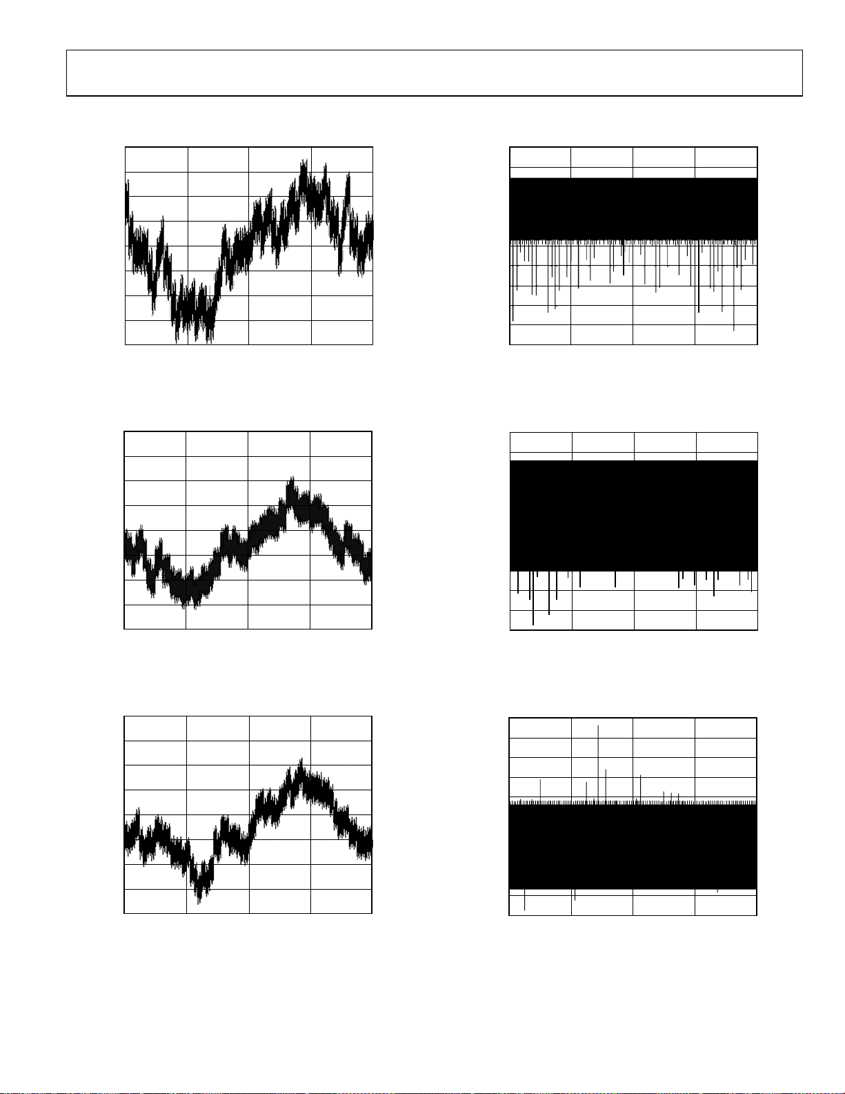
Figure 58. Eye Diagram of Data Source Used in Building the 600 MHz Timing
Data Array of Table 14
Over temperature, the valid sampling window shifts. Therefore,
when attempting operation of the device over 500 MHz, the
timing must be optimized again whenever the device undergoes
a temperature change of more than 20
o
C. Another consideration
in the timing of the digital data port is the propagation delay
variation from the clock output (DCOP/DCON) to the clock
input. If this varies significantly over time (more than 25% of
SET or HLD) due to temperature changes or other effects,
repeat this timing calibration procedure.
At sample rates of ≤400 MSPS, the interface timing margin is
sufficient to allow for a simplified procedure. In this case, the
SEEK bit can be recorded as SMP is swept through the range
from 0 to 31. The center of the first valid sampling window can
then be chosen as the optimal value of SMP. Using the 400 MHz
case from Tabl e 14 as an example, the first valid sampling
window occurs for SMP values of 7 to 13. The center of this
window is 10, so 10 can be used as the optimal SMP value.
DRIVING THE CLK INPUT
The CLK input requires a low jitter differential drive signal. It is
a PMOS input differential pair powered from the 1.8 V supply;
therefore, it is important to maintain the specified 400 mV
input common-mode voltage. Each input pin can safely swing
from 200 mV p-p to 1 V p-p about the 400 mV common-mode
voltage. While these input levels are not directly LVDS-compatible,
CLK can be driven by an offset ac-coupled LVDS signal, as
shown in Figure 59.
LVDS_P_IN CLKP
LVDS_N_IN CLKN
If a clean sine clock is available, it can be transformer-coupled
to CLKP and CLKN as shown in Figure 60. Use of a CMOS or
TTL clock is also acceptable for lower sample rates. It can be
routed through a CMOS-to-LVDS translator, and then ac-
0.1µF
50Ω
V
= 400mV
50Ω
0.1µF
CM
Figure 59. LVDS DAC CLK Drive Circuit
06936-056
50Ω
CLKN
BAV99ZXCT
HIGH SPEED
DUAL DIODE
= 400mV
V
CM
06936-057
Figure 60. TTL or CMOS DAC CLK Drive Circuit
A simple bias network for generating the 400 mV commonmode voltage is shown in Figure 61. It is important to use
CVDD18 and CGND for the clock bias circuit. Any noise or
other signal coupled onto the clock is multiplied by the DAC
digital input signal and can degrade the DAC’s performance.
= 400mV
CM
1nF
CVDD18
CGND
06936-058
1kΩ
87Ω
0.1µF 1nF
Figure 61. DAC CLK VCM Generator Circuit
FULL-SCALE CURRENT GENERATION
Internal Reference
Full-scale current on the I DAC and Q DAC can be set from
8.66 mA to 31.66 mA. Initially, the 1.2 V band gap reference is
used to set up a current in an external resistor connected to
FS ADJ (Pin 54). A simplified block diagram of the reference
circuitry is shown in Figure 62. The recommended value for
the external resistor is 10 kΩ, which sets up an I
resistor of 120 μA, which in turn provides a DAC output fullscale current of 20 mA. Because the gain error is a linear function
of this resistor, a high precision resistor improves gain matching
to the internal matching specification of the devices. Internal
current mirrors provide a current-gain scaling, where I DAC or
Q DAC gain is a 10-bit word in the SPI port register. The default
value for the DAC gain registers gives a full-scale current output
(I
) of approximately 20 mA, where IFS is equal to
FS
= (86.6 + (0.220 × DAC gain)) × 1000/R
I
FS
AD9783
I DAC GAIN
CURRENT
SCALING
Q DAC GAIN
I DAC
DAC FULL-S CALE
REFERENCE CURRENT
Q DAC
.1µF
1.2V BAND GAP
REFIO
FS ADJ
10kΩ
Figure 62. Reference Circuitry
REFERENCE
in the
06936-059
Rev. A | Page 26 of 36
Page 27
AD9780/AD9781/AD9783
35
30
25
20
(mA)
FS
I
15
10
5
0 256 512 768 1024
DAC GAIN CODE
Figure 63. I
vs. DAC Gain Code
FS
06936-060
DAC TRANSFER FUNCTION
Each DAC output of the AD9780/AD9781/AD9783 drives two
complementary current outputs, I
a near I
when all bits are high. For example,
FS
N
DAC CODE = 2
− 1
OUTP
and I
where N = 12/14/16 bits for AD9780/AD9781/AD9783
(respectively), while I
The current output appearing at I
both the input code, and I
= (DAC DATA/2N) × IFS (1)
I
OUTP
I
= ((2N − 1) − DAC DATA)/2N × IFS (2)
OUTN
where DAC DATA = 0 to 2
provides no current.
OUTN
and I
OUTP
and can be expressed as
FS
N
− 1 (decimal representation).
The two current outputs typically drive a resistive load directly
or via a transformer. If dc coupling is required, I
should be connected to matching resistive loads (R
tied to analog common (AVSS). The single-ended voltage
output appearing at the I
V
= I
= I
OUTP
OUTN
× R
× R
V
OUTP
OUTN
and I
OUTP
(3)
LOAD
(4)
LOAD
OUTN
pins is
Note that to achieve the maximum output compliance of 1 V at
the nominal 20 mA output current, R
Also note that the full-scale value of V
LOAD
OUTP
not exceed the specified output compliance range to maintain
specified distortion and linearity performance.
There are two distinct advantages to operating the AD9780/
AD9781/AD9783 differentially. First, differential operation
helps cancel common-mode error sources associated with I
and I
, such as noise, distortion, and dc offsets. Second, the
OUTN
differential code-dependent current and subsequent output
voltage (V
output (V
V
) is twice the value of the single-ended voltage
DIFF
DIFF
OUTP
= (I
or V
OUTP
), providing 2× signal power to the load.
OUTN
– I
OUTN
) × R
(5)
LOAD
. I
OUTP
OUTP
LOAD
provides
and I
OUTN
) that are
OUTN
is a function of
OUTN
must be set to 50 Ω.
and V
OUTN
should
OUTP
ANALOG MODES OF OPERATION
The AD9780/AD9781/AD9783 use a proprietary quad-switch
architecture that lowers the distortion of the DAC by eliminating a
code-dependent glitch that occurs with conventional dual-switch
architectures. This architecture eliminates the code-dependent
glitches, but creates a constant glitch at a rate of 2 × f
communications systems and other applications requiring good
frequency domain performance from the DAC, this is seldom
problematic.
The quad-switch architecture also supports two additional
modes of operation: mix mode and return-to-zero mode. The
waveforms of these two modes are shown in Figure 64. In mix
mode, the output is inverted every other half clock cycle. This
effectively chops the DAC output at the sample rate. This chopping has the effect of frequency shifting the sinc roll-off from dc
to f
. Additionally, there is a second subtle effect on the output
DAC
spectrum. The shifted spectrum is also shaped by a second sinc
function with a first null at 2 × f
. The reason for this shaping
DAC
is that the data is not continuously varying at twice the clock
rate, but is simply repeated.
In return-to-zero mode, the output is set to midscale every
other half clock cycle. The output is similar to the DAC output
in normal mode except that the output pulses are half the width
and half the area. Because the output pulses have half the width,
the sinc function is scaled in frequency by two and has a first
null at 2 × f
. Because the area of the pulses is half that of the
DAC
pulses in normal mode, the output power is half the normal
mode output power.
INPUT DATA
DAC CLK
QUAD-SWITCH
DAC OUTPUT
(
f
MIX MODE)
S
QUAD-SWITCH
DAC OUTPUT
(RETURN-TO -
ZERO MODE)
Figure 64. Mix Mode and Return-to-Zero Mode DAC Waveforms
1
D9D8D7D6D5D4D3D2D
The functions that shape the output spectrums for the three
modes of operation, normal mode, mix mode, and return-tozero mode, are shown in Figure 65. Switching between the
analog modes reshapes the sinc roll-off inherent at the DAC
output. This ability to change modes in the AD9780/AD9781/
AD9783 makes the parts suitable for direct IF applications. The
user can place a carrier anywhere in the first three Nyquist
zones depending on the operating mode selected. The performance and maximum amplitude in all three Nyquist zones is
. For
DAC
D
10
t
t
06936-061
Rev. A | Page 27 of 36
Page 28

AD9780/AD9781/AD9783
V
A
impacted by this sinc roll-off depending on where the carrier is
placed, as shown in Figure 65.
0
–10
–20
T(f) (dB)
–30
–40
Figure 65. Transfer Function for Each Analog Operating Mode
MIX
NORMAL
0.5011.0 2.0
RETURN-TO-Z ERO
f
)
(
S
.5
06936-062
Auxiliary DACs
Two auxiliary DACs are provided on the AD9780/AD9781/
AD9783. A functional diagram is shown in Figure 66. The
auxiliary DACs are current output devices with two output
pins, AUXP and AUXN. The active pin can be programmed to
either source or sink current. When either sinking or sourcing,
the full-scale current magnitude is 2 mA. The available compliance
range at the auxiliary DAC outputs depends on whether the output
is configured to sink or source current. When sourcing current,
the compliance voltage is 0 V to 1.6 V, but when sinking current,
the output compliance voltage is reduced to 0.8 V to 1.6 V. Either
output can be used, but only one output of the AUX DAC (P or
N) is active at any time. The inactive pin is always in a high
impedance state (>100 kΩ).
0m
TO
BIAS
2mA
0mA
2mA
TO
SINK
OR
SOURCE
POSITIVE
OR
NEGATIVE
AUXP
AUXN
06936-063
Figure 66. Auxiliary DAC Functional Diagram
In a single sideband transmitter application, the combination of
the input referred dc offset voltage of the quadrature modulator
and the DAC output offset voltage can result in local oscillator
(LO) feedthrough at the modulator output, which degrades system
performance. The auxiliary DACs can be used to remove the dc
offset and the resulting LO feedthrough. The circuit configuration for using the auxiliary DACs for performing dc offset
correction depends on the details of the DAC and modulator
interface. An example of a dc-coupled configuration with lowpass filtering is shown in Figure 67.
QUADRATURE
MODULATOR V+
AD9783
AUX
DAC1 OR
DAC2
AD9783
DAC1 OR
DAC2
25Ω TO 50Ω
OPTIONAL
PASSIVE
FILTERING
Figure 67. DAC DC-Coupled to Quadrature Modulator with a Passive DC Shift
QUAD MOD
I OR Q INPUTS
25Ω TO 50Ω
06936-064
Rev. A | Page 28 of 36
Page 29

AD9780/AD9781/AD9783
POWER DISSIPATION
Figure 68 through Figure 73 show the power dissipation of the part in single DAC and dual DAC modes.
0.50
0.45
0.40
0.35
0.30
0.25
0.20
POWER (W)
0.15
0.10
0.05
0
0 100 200 300 400 500
CLOCK SPEED (MSPS)
Figure 68. Power Dissipation, I Data Only, Single DAC Mode
0.200
0.175
0.150
0.125
0.100
POWER (W)
0.075
0.050
0.025
DVDD18
CVDD
0.50
0.45
0.40
0.35
0.30
0.25
0.20
POWER (W)
0.15
0.10
0.05
0
0 100 200 300 400 500
06936-065
CLOCK SPEED (MSPS)
06936-068
Figure 71. Power Dissipation, I and Q Data, Dual DAC Mode
0.200
0.175
0.150
0.125
0.100
POWER (W)
0.075
0.050
0.025
DVDD18
CVDD
0
0 100 200 300 400 500
CLOCK SPEED (M SPS)
Figure 69. Power Dissipation, Digital 1.8 V Supply, Clock 1.8 V Supply,
I Data Only
0.200
0.175
0.150
0.125
0.100
POWER (W)
0.075
0.050
0.025
0
0 100 200 300 400 500
AVDD33
DVDD33
CLOCK SPEED (M SPS)
Figure 70. Power Dissipation, Digital 3.3 V Supply, Analog 3.3 V Supply,
I Data Only
0
0 100 200 300 400 500
06936-066
CLOCK SPEED (MSPS)
06936-069
Figure 72. Power Dissipation, Digital 1.8 V Supply, Clock 1.8 V Supply,
I and Q Data, Dual DAC Mode
0.200
0.175
0.150
0.125
0.100
POWER (W)
0.075
0.050
0.025
0
0 100 200 300 400 500
06936-067
AVDD33
DVDD33
CLOCK SPEED (MSPS)
06936-070
Figure 73. Power Dissipation, Digital 3.3 V Supply, Analog 3.3 V Supply,
I and Q Data, Dual DAC Mode
Rev. A | Page 29 of 36
Page 30

AD9780/AD9781/AD9783
EVALUATION BOARD SCHEMATICS
BLACK
TP7
J587
J7
BLACK
TP8
J587
J8
CVDD18
RED
TP1
C37
0.1UF
10UF
C15
L1
L1812
TP2
EXC-CL4532U1
C36
0.1UF
06936-077
DVDD18
RED
0.1UF
10UF
C16 C42
L2
L1812
EXC-CL4532U1
C38
0.1UF
DVDD33
RED
TP3
0.1UF
10UF
C17 C43
L3
L1812
EXC-CL4532U1
C39
0.1UF
AVDD33
RED
TP4
0.1UF
10UF
C18 C44
L4
L1812
EXC-CL4532U1
C40
0.1UF
DVCC33
RED
TP6
0.1UF
10UF
C19 C45
L6
L1812
EXC-CL4532U1
C41
0.1UF
C21
100UF
10V
CCASE
J587
R0805
J1
R30 DNP
3
GND
7
SD
IN OUT
VR4 ADP3333ARM-1.8
21
C49
5VIN
C66
100UF
10V
J587
CCASE
B1
J587
B2
0.1UF
5VIN
10V
100UF
C22
CCASE
J587
R0805
J2
R29 DNP
3
GND
7
SD
IN OUT
VR5 ADP3333ARM-1.8
21
5VIN
C23
100UF
10V
CCASE
J587
R0805
J3
R18 DNP
3
GND
7
SD
IN OUT
VR1 ADP3333ARM-3.3
21
C46
C50
0.1UF
0.1UF
5VIN
10V
100UF
C24
CCASE
J587
R0805
J4
R19 DNP
3
GND
7
SD
IN OUT
VR2 ADP3333ARM-3.3
21
C47
0.1UF
5VIN
10V
100UF
C26
CCASE
J587
R0805
J6
R28 DNP
3
GND
7
SD
IN OUT
VR3 ADP3333ARM-3.3
21
C48
0.1UF
5VIN
Figure 74. Power Distribution
Rev. A | Page 30 of 36
Page 31

AD9780/AD9781/AD9783
0
6936-078
P1
1
2
R0805
R0805
7.5KR12
R11 7.5K
R0805
R13 7.5K
6
453
C0402
0.1UF
C10
L1210
L7 10UH
DVDD33
C9
0.1UF
C0402
R16
20K
R0805
20K
R15R14
R0805
20K
R0805
DVDD33
4
11
U9
U9
U9
12 13
74HC14
12
U9
U9
74HC14
89
10
74HC14
56
U9
43
74HC14
U8
74HC14
1
DVDD33
74HC14
2
3
74HC125
10KR17
R0805
10
U8
13
12
U8
74HC125
11
5
U8
74HC125
6
74HC125
89
10K
R0805
10K
R27 R26
R0805
3
4
SW6
3
2
SW1
SW2
1
DVDD33
SPI_CSB
3
2
3
SW3
1
1
SPI_SDI
SPI_CLK
2
3
2
SW4
1
2
1
U1
3
1
2
32
DVDD33
MR
41
VCCGND
A1
RST
SPI_SDO
5
4
U1
6
3
SW5
RESET
DVDD33
2
DVDD33
1
U1
7
14
0.1UF
C51
C0402
Figure 75. SPI Interface
Rev. A | Page 31 of 36
Page 32
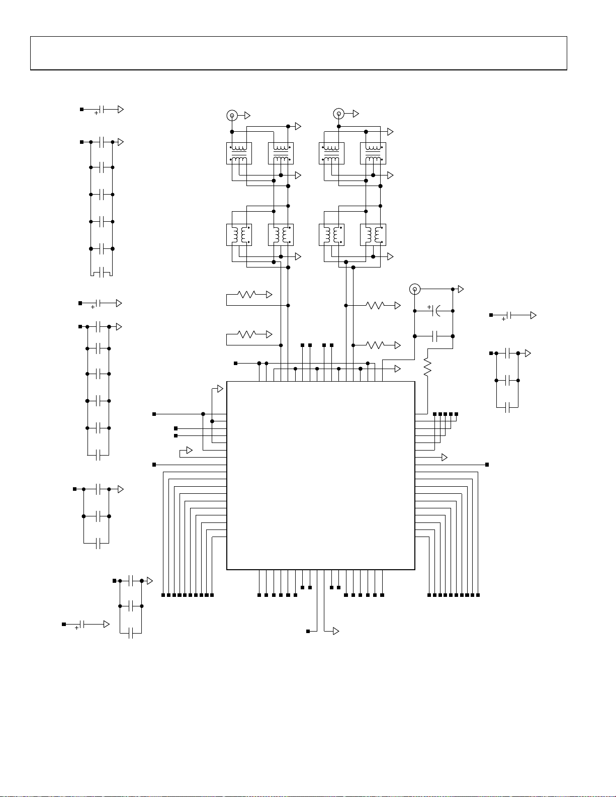
AD9780/AD9781/AD9783
AVDD33
10UF
C29
AVDD33
0.1UF
C8
C0402
0.1UF
C7
C0402
C58
100PF
C57
100PF
1000PF
C59
C0402 C0402C0402C0402
1000PF
C56
10UF
C28
CVDD18
0.1UF
C2
CVDD18
C0402
0.1UF
C1
C0402C0402C0402C0402
C61
100PF
C62
100PF
C60
C63
1000PF
C0402 C0402C0402C0402
1000PF
CVDD18
CLKP
CLKN
DVSS
DVDD18
0.1UF
C3
DVDD18
C52
100PF
C53
1000PF
1
4
5
8
9
10
11
12
13
14
15
16
17
18
ADT2-1T-1P
ADTL1-12
CVDD18
CVSS
CLKP
CLKN
CVSS
CVDD18
DVSS
DVDD18
D13P
D13N
D12P
D12N
D11P
D11N
D10P
D10N
D9P
D9N
S4
5
1
23
2:1
T5
4
5
15
23
PS
T2
4
R2
49.9-0.5%
R0402
R1
49.9-0.5%
R0402
AVDD33
72
AVDD33
2:1
T6
T3
TC2-1T
1234
5
43
SP
TC1-1-13M
2
1
AUX1P
68
69770
71
AVSS
AVSS
AUX1P
IOUT1P
IOUT1N
AVDD33
S7
5
1
23
2:1
ADT2-1T-1P
ADTL1-12
T10
4
5
15
23
PS
T7
4
2:1
T11
TC2-1T
1234
5
T8
SP
TC1-1-13M
1234
S8
R4
49.9-0.5%
R0402
R3
AUX1N
AUX2N
AUX2P
6364656667
AVSS
AVSS
AUX2P
AUX2N
AUX1N
49.9-0.5%
R0402
55
56
57
58
596606162
AVSS
REFIO
IOUT2P
IOUT2N
AVDD33
AVDD33
FS ADJ
RESET
SCLK
SDIO
DVSS
DVDD18
CSB
SDO
D0N
D0P
D1N
DIP
D2N
D2P
C27
16V
4.7UF
0.1UF
C6
C0402
DVDD18
DVDD18
R0603
R5
10K-0.1%
RESET
CSB
SCLK
SDIO
SDO
54
53
52
51
50
49
48
47
46
NC
45
NC
44
NC
43
NC
42
41
40
39
38
37
DVSS
DVDD18
06936-079
10UF
C20
C0402
C5
0.1UF
C0402C0402
C54
100PF
C55
1000PF
D8P
D8N
D7P
D7N
D6P
D6N
DCOP
DCON
DVDD33
DVSS
IDCIP
DCIN
0.1UF
C4
C0402
DVDD33
C64
100PF
C0402C0402
DVDD33
10UF
C25
C65
D13P
D11P
D12P
D11N
D12N
D13N
1000PF
D10P
D10N
U7
D9P
D9N
192202122232425262728
D8P
D6N
D7N
D8N
DCOP
DCON
D6P
D7P
DVDD33
29330313233343536
DCIP
DCIN
DVSS
D3P
D4N
D4P
D5N
D5P
D5P
D3N
NC
D3P
D4P
D3N
D4N
D5N
D1P
D2P
D2N
NCNCNC
D0P
D0N
D1N
Figure 76. Main Schematic
Rev. A | Page 32 of 36
Page 33

AD9780/AD9781/AD9783
D04_P
D10_N
D11_N
D08_N
D09_N
DCLKI_N
DCLKO_N
D07_N
D06_N
D04_N
D05_N
D02_N
D03_N
D00_N
D01_N
L8 10UH
D00_P
L1210
J9
L9 10UH
L1210
FCN-268 F024-G/0 D
D01_P
D02_P
D03_P
D05_P
D07_P
D06_P
DCLKI_P
DCLKO_P
D08_P
D09_P
D11_P
D10_P
06936-080
Jack
G49 G50
S47 S48
G47 G48
S45 S46
G45 G46
S43 S44
G43 G44
S41 S42
G41 G42
S39 S40
G39 G40
S37 S38
G37 G38
S35 S36
G35 G36
S33 S34
G33 G34
S31 S32
G31 G32
S29 S30
G29 G30
S27 S28
G27 G28
S25 S26
G25 G26
S23 S24
G23 G24
S21 S22
G21 G22
S19 S20
G19 G20
S17 S18
G17 G18
S15 S16
G15 G16
S13 S14
G13 G14
S11 S12
G11 G12
S9 S10
G9 G10
S7 S8
G7 G8
S5 S6
G5 G6
S3 S4
G3 G4
S1
G1
Jack
D15_P
D14_P
D13_P
D12_P
D12_N
D13_N
D14_N
D15_N
S2
G2
Figure 77. Data Input Detail
Rev. A | Page 33 of 36
Page 34
AD9780/AD9781/AD9783
R0402
S10
S9
R10
AUX1_N
AUX1_P
CLK_N
25
S11
AUX2_N
S12
AUX2_P
CLK_P
R8
25
R0402
06936-081
C11
DNP
R6
R0402
C0402C0402
C0402
1K
TC1-1-13M
0.1UF
C12
R7
R0402
2
1
SP
T1
5
43
R9
VAL
R0402
C0402
300
C14
0.1UF
C13
CVDD18
0.1UF
S1
Figure 78. AUX DAC and Clock Input Circuit Details
Rev. A | Page 34 of 36
Page 35

AD9780/AD9781/AD9783
C
OUTLINE DIMENSIONS
0.60
0.42
0.24
55
54
(BOTTOM VIEW)
EXPOSED
PAD
72
1
PIN 1
INDICATOR
4.70
BSC SQ
INDI
PIN 1
ATO R
10.00
BSC SQ
TOP VI EW
9.75
BSC SQ
0.60
0.42
0.24
0.50
BSC
1.00
0.85
0.80
SEATING
PLANE
12° MAX
0.50
0.40
0.30
0.80 MAX
0.65 TYP
0.30
0.23
0.18
COMPLIANT TO JEDEC STANDARDS MO-220-VNND- 4
0.05 MAX
0.02 NOM
0.20 REF
COPLANARIT Y
0.08
37
36
8.50 REF
18
19
EXPOSED PAD MUST BE
SOLDERED TO PCB AND
CONNECT ED TO AVSS.
111507-A
Figure 79. 72-Lead Lead Frame Chip Scale Package [LFCSP_VQ]
10 mm × 10 mm, Very Thin Quad
(CP-72-1)
Dimensions shown in millimeters
ORDERING GUIDE
Model Temperature Range Package Description Package Option
AD9780BCPZ
AD9780BCPZRL
AD9781BCPZ
AD9781BCPZRL
AD9783BCPZ
AD9783BCPZRL
AD9780-EBZ
AD9781-EBZ
AD9783-EBZ
1
Z = RoHS Compliant Part.
1
−40°C to +85°C 72-Lead LFCSP_VQ CP-72-1
1
−40°C to +85°C 72-Lead LFCSP_VQ CP-72-1
1
−40°C to +85°C 72-Lead LFCSP_VQ CP-72-1
1
−40°C to +85°C 72-Lead LFCSP_VQ CP-72-1
1
−40°C to +85°C 72-Lead LFCSP_VQ CP-72-1
1
−40°C to +85°C 72-Lead LFCSP_VQ CP-72-1
1
Evaluation Board
1
Evaluation Board
1
Evaluation Board
Rev. A | Page 35 of 36
Page 36

AD9780/AD9781/AD9783
NOTES
©2007–2008 Analog Devices, Inc. All rights reserved. Trademarks and
registered trademarks are the property of their respective owners.
D06936-0-6/08(A)
Rev. A | Page 36 of 36
 Loading...