

Page 1
PRELIMINAR Y TECHNICAL D A T A
a
12-Bit, 160 MSPS
××
×/4
××
××
×/8
××
2
®
Dual TxDAC+
××
× Interpolating
××
D/A Converter
Preliminary Technical Data
FEATURES
01-19-01
12 bit Resolution, 160 MSPS Conversion Rate
Selectable 2×/4×/8× Interpolating Filter
Programmable Channel Gain and Offset Adjustment
Fs/2,4,8 Digital Quadrature Modulation Capability
Direct IF Transmission Mode for 70MHz+ IFs
Enables Image Rejection Architecture
Fully Compatible SPI Port
Excellent AC Performance
- SFDR -69dBc @ 2-35MHz
-WCDMA ACPR -70dB @ IF=16.25 MHz
Internal PLL Clock Multiplier
Selectable Internal Clock Divider
Versatile Clock Input
-Differential/Single Ended
-Sine W ave or TTL/CMOS/LVPECL Compatible
Versatile Input Data Interface
-2’s Complement/Straight Binary Data Coding
-Dual Port or Single Port Interleaved Data
Single +3.3V Supply Operation
Power Dissipation: <700 mW @ 3.3V
On-chip 1.2 V Reference, 80-Lead LQFP
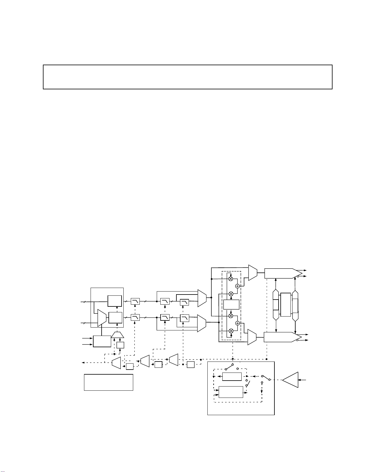
PROGRAMABLE DUAL INTERPOLATION DAC
WITH IMAGE REJECTION/DIGITAL MODULATION
AD9773
APPLICATIONS
Communications:
Analog Quadrature Modulation Architectures
3G, Multi-Carrier GSM, TDMA, CDMA Systems
Multi-Level QAM Modulators, Instrumentation
PRODUCT DESCRIPTION
The AD9773 is the 12 bit member of the AD977x family of
pin-compatible, high performance, programmable 2×/4×/8×
interpolating TxDAC+s. The AD977x family features a serial
port interface (SPI) providing a high level of programmability thus allowing for enhanced system level options. These
options include: selectable 2×/4×/8× interpolation filters;
Fs/2, Fs/4 or Fs/8 digital quadrature modulation with image
rejection; a direct IF mode; programmable channel gain
and offset control; programmable internal clock divider;
straight binary or two’s complement data interface; and a
single port or dual port data interface.
I AND Q
NO NINTE RLE AV ED
OR INTERLEAVED DATA
WRITE
SELECT
CLOCK OUT
HALF-B AND
I
LATCH
Q
LATCH
FILTER #1*
12
12
⫼2
⫼2
DATA
ASSEMBLER
12
12
MUX
CONTROL
SPI INTERFACE &
CONTROL REGISTERS
*Half-Band Filters also can be configured for "Zero-Stuffing Only"
HALF-B AND
22
22
FILTER #2*
⫼2
HALF-B AND
22
22
REV. PrA
BLOCK DIAGRAM
Information furnished by Analog Devices is believed to be accurate and
reliable. However, no responsibility is assumed by Analog Devices for its
use, nor for any infringements of patents or other rights of third parties
which may result from its use. No license is granted by implication or
otherwise under any patent or patent rights of Analog Devices.
I DAC
COS
FILTER#3*
22
22
FILTER
BYPASS MUX
⫼2
PLL CLO CK MULTIP LIER
One Technology Way, P.O. Box 9106, Norwood, MA 02062-9106, U.S.A.
Tel: 781/329-4700 World Wide Web Site: http://www.analog.com
Fax: 781/326-8703 © Analog Devices, Inc., 2000
+
-/+
SIN
/2,4,8
F
DAC
SIN
+/-
+
COS
(F
)
DAC
PRESCALER
PHASE DETEC
TOR & VCO
AND CLOCK DIVIDER
DAC MODE B YPASS MUX
IMAGE REJE CTION/DUAL
-
I DAC
GAIN
DAC
VREF
I/Q DAC
Q DAC
I
OUT
OFFSET
DAC
I OFFSET
REGISTERS
GAIN/OFFSET
I
OUT
DIFF.
REFCLK
1
Page 2

AD9773
REV. PrA
PRELIMINAR Y TECHNICAL D A T A
PRODUCT DESCRIPTION (Continued)
The selectable 2×/4×/8× interpolation filters simplify the
requirements of the reconstruction filters while simultaneously enhancing the TxDAC+ family’s passband noise/
distortion performance. The independent channel gain and
offset registers allow the user to calibrate LO feedthrough
and sideband suppression errors associated with analog
quadrature modulators. The 6 dB of gain adjustment range
also can be used to control the output power level of each
DAC.
The AD9773 features the ability to perform Fs/4 and Fs/8
digital modulation and image rejection when combined
with an analog quadrature modulator. In this mode, the
AD9773 would accept I and Q complex data (representing a
single or multicarrier waveform), generate a quadrature
modulated IF signal along with its orthogonal representation via its dual DACs, and present these two reconstructed orthogonal IF carriers to an analog quadrature
modulator to complete the image rejection upconversion
process. Another digital modulation mode (i.e. the Direct
IF Mode) allows the original baseband signal representation to be frequency translated such that pairs of images
fall at multiples of 1/2 the DAC update rate.
The AD9773 family includes a flexible clock interface
accepting differential or single-ended sinewave or digital
logic inputs. An internal PLL clock multiplier is also
included to generate the necessary on-chip high frequency
clocks. It can also be disabled to allow the use of a higher
performance external clock source. An internal programmable divider simplifies clock generation in the converter
when using an external clock source. A flexible data input
interface allows for straight binary or 2’s complement
formats as well as supports single port interleaved or dual
port data.
PRODUCT HIGHLIGHTS
1. The AD9773 is the 12 bit member of the AD977x family of
pin-compatible, high performance, programmable 2×/4×/8×
interpolating TxDAC+s.
2. Direct IF Transmission capability for 70MHz +IFs
through a novel digital mixing process
3. Fs/8 Digital Quadrature Modulation and user selectable
image rejection to simplify /remove cascaded SA W filter
stages
4. 2×/4×/8× User Selectable Interpolating Filter eases data
rate and output signal reconstruction filter requirements.
5. User selectable 2’s Complement/Straight Binary Data
Coding.
6. User programmable Channel Gain Control over 1 dB
range in 0.01dB increments
7. User programmable Channel Offset +/-10% over the FSR
8. Ultra high speed 400 MSPS DAC conversion rate.
9. Internal Clock Divider provides data rate clock for easy
interfacing.
10. Flexible Clock Input with Single Ended or Differential
Input, CMOS or 1V p-p LO Sinewave input capability .
11. Low Power: Complete CMOS DAC operates on <700
mW from a 3.0V to 3.6V single supply. The 20ma full-scale
current can be reduced for lower power operation, and a
several sleep functions are provided to reduce power
during idle periods.
12. On-chip V oltage Reference: The AD9773 includes a 1.20
V temperature-compensated bandgap voltage reference.
13. Small 80 lead LQFP
Dual high performance TxDAC+s provides a differential
current output programmable over a 0-20mA range. The
AD9773 is manufactured on an advanced 0.35 micron
CMOS process, operates from a single supply of 3.0V to 3.6
V and consumes <700 mW of power.
T argeted at wide dynamic range, Multi-Carrier and MultiStandard systems, the superb baseband performance of the
AD9773 is ideal for Wideband-CDMA, Multi-Carrier
CDMA, Multi-Carrier TDMA, Multi-Carrier GSM and high
performance systems employing high order QAM modulation schemes. The image rejection feature simplifies and
can help to reduce the number of signal band filters needed
in an transmit signal chain. The direct IF mode helps to
eliminate a costly mixer stage for a variety of communica-
tions systems.
2
Page 3

PRELIMINAR Y TECHNICAL D A TA
REV. PrA
AD9773–SPECIFICATIONS
DC SPECIFICATIONS (T
MIN
to T
, AVDD = +3.3 V, CLKVDD = +3.3 V, DVDD = +3.3 V, PLLVDD = +3.3v, I
MAX
OUTFS
= 20 mA,
unless otherwise noted)
PARAMETER MIN TYP MAX UNITS
RESOLUTION 12 bits
DC Accuracy
1
Integral Non-Linearity LSB
Differential Non_Linearity LSB
Monotonicity
ANALOG OUTPUT
Offset Error % of FSR
Gain Error (Without Internal Reference) % of FSR
Gain Error (With Internal Reference) % of FSR
Full-Scale Output Current
2
20 mA
Output Compliance Range –1.0 +1.25 V
Output Resistance 200 kΩ
Output Capacitance 3 pF
REFERENCE OUTPUT
Reference Voltage 1.14 1.20 1.26 V
Reference Output Current
3
1µA
REFERENCE INPUT
Input Compliance Range 0.1 1.25 V
Reference Input Resistance (REFLO = 3 V) 10 MΩ
Small Signal Bandwidth 0.5 MHz
TEMPERATURE COEFFICIENTS
Unipolar Offset Drift ppm of FSR/°C
Gain Drift (Without Internal Reference) ppm of FSR/°C
Gain Drift (With Internal Reference) ppm of FSR/°C
Reference Voltage Drift ppm/°C
POWER SUPPLY
AVDD
Voltage Range 3.0 3.3 3.6 V
Analog Supply Current (I
I
in SLEEP Mode mA
AV DD
)mA
AVDD
CLKVDD
Voltage Range 3.0 3.3 3.6 V
Clock Supply Current (I
)mA
CLKVDD
PLLVDD
Voltage Range 3.0 3.3 3.6 V
PLL Multiplier Supply Current (I
)mA
PLLVDD
DVDD
Voltage Range 3.0 3.3 3.6 V
Digital Supply Current (I
)mA
DVDD
Nominal Power Dissipation <700 mW
Power Supply Rejection Ratio – AVDD % of FSR/V
Power Supply Rejection Ratio – DVDD % of FSR/V
OPERATING RANGE –40 +85 °C
NOTES
1
Measured at I
2
Nominal full-scale current, I
3
Use an external amplifier to drive any external load.
Specifications subject to change without notice.
driving a virtual ground.
OUTA
OUTFS
, is 32× the I
current.
REF
3
Page 4

PRELIMINAR Y TECHNICAL D A TA
REV. PrA
AD9773–SPECIFICATIONS
(T
to T
DYNAMIC SPECIFICATIONS
MIN
Differential Transformer Coupled Output, 50Ω Doubly Terminated, unless otherwise noted)
Parameter Min Typ Max Units
DYNAMIC PERFORMANCE
Maximum DAC Output Update Rate (f
Output Settling Time (t
Output Propagation Delay
Output Rise Time (10% to 90%)
Output Fall Time (10% to 90%)
Output Noise (I
OUTFS
) (to 0.025%) ns
ST
1
(tPD) ns
2
2
= 20 mA) pA√Hz
) 400 MSPS
DAC
AC LINEARITY–BASEBAND MODE
Spurious-Free Dynamic Range (SFDR) to Nyquist (f
f
= MSPS; f
DATA
= MSPS; f
f
DATA
= MSPS; f
f
DATA
f
= MSPS; f
DATA
= MSPS; f
f
DATA
= MSPS; f
f
DATA
= MHz dBc
OUT
= MHz dBc
OUT
= MHz dBc
OUT
= MHz dBc
OUT
= MHz dBc
OUT
= MHz dBc
OUT
Two-Tone Intermodulation (IMD) to Nyquist (f
= MSPS; f
f
DATA
f
= MSPS; f
DATA
f
= MSPS; f
DATA
= MSPS; f
f
DATA
f
= MSPS; f
DATA
f
= MSPS; f
DATA
= MHz; f
OUT1
= MHz; f
OUT1
= MHz; f
OUT1
= MHz; f
OUT1
= MHz; f
OUT1
= MHz; f
OUT1
OUT2
OUT2
OUT2
OUT2
OUT2
= MHz dBc
OUT2
Total Harmonic Distortion (THD)
= MSPS; f
f
DATA
f
= MSPS; f
DATA
= MHz; 0 dBFS dB
OUT
= MHz; 0 dBFS dB
OUT
Signal-to-Noise Ratio (SNR)
= MSPS; f
f
DATA
= MSPS; f
f
DATA
= MHz; 0 dBFS dB
OUT
= MHz; 0 dBFS dB
OUT
Adjacent Channel Power Ratio (ACPR)
WCDMA with MHz BW, MHz Channel Spacing
IF = 16 MHz, f
IF = 32 MHz, f
= 65.536 MSPS dBc
DATA
= 131.072 MSPS dBc
DATA
Four-Tone Intermodulation
MHz, MHz, MHz and MHz at –12 dBFS dBFS
(f
= MSPS, Missing Center)
DATA
AC LINEARITY–IF MODE
Four-Tone Intermodulation at IF = MHz
MHz, MHz, MHz and MHz at dBFS dBFS
f
= MSPS, f
DATA
NOTES
1
Propagation delay is delay from CLK input to DAC update.
2
Measured single-ended into 50 Ω load.
Specifications subject to change without notice.
= MHz
DAC
, AVDD = +3.3 V, CLKVDD = +3.3 V, DVDD = +3.3 V, PLLVDD = 0 V, I
MAX
ns
ns
= 0 dBFS)
OUT
= f
OUT1
= –6 dBFS)
OUT2
= MHz dBc
= MHz dBc
= MHz dBc
= MHz dBc
= MHz dBc
OUTFS
= 20 mA,
4
Page 5

PRELIMINAR Y TECHNICAL D A TA
REV. PrA
AD9773–SPECIFICATIONS
(T
to T
DIGITAL SPECIFICATIONS
Parameter Min Typ Max Units
DIGITAL INPUTS
Logic “1” Voltage 2.1 3 V
Logic “0” Voltage 0 0.9 V
Logic “1” Current
Logic “0” Current –10 +10 µA
Input Capacitance 5 pF
CLOCK INPUTS
Input Voltage Range 0 3 V
Common-Mode Voltage 0.75 1.5 2.25 V
Differential Voltage 0.5 1.5 V
PLL CLOCK ENABLED
Input Setup Time (tS) 0.2 ns
Input Hold Time (t
Latch Pulsewidth (t
PLL CLOCK DISABLED
Input Setup Time (t
Input Hold Time (t
Latch Pulsewidth (t
CLK/PLLLOCK Delay (tOD) TBD ns
1
) 1.8 ns
H
) 1.5 ns
LPW
) -1.2 ns
S
) 3.2 ns
H
) 1.5 ns
LPW
MIN
mA, unless otherwise noted)
, AVDD = +3.3 V, CLKVDD = +3.3 V, PLLVDD = +0 V, DVDD = +3.3 V, I
MAX
–10 +10 µA
OUTFS
= 20
Specifications subject to change without notice.
ORDERING GUIDE
Temperature Package Package
Model Range Description Option*
AD9773AST –40°C to +85°C 80-Lead LQFP ST-80
AD9773EB Evaluation Board
*ST = Thin Plastic Quad Flatpack.
5
Page 6

PRELIMINAR Y TECHNICAL D A TA
REV. PrA
AD9773–SPECIFICATIONS
CLKVDD
LPF
CLKVDD
CLKCOM
CLK+
CLK-
CLKCOM
DATACLK/PLL_LOCK
DCOM
DVDD
P1B11(MSB)
P1B10
P1B9
P1B8
P1B7
P1B6
DVDD
DCOM
P1B5
P1B4
OUTA1IOUTB1
AVDD
ACOM
AVDD
ACOM
80 79 78 77 76 75 74 73 72 71 70 69 68 67 66 65 64 63 62 61
1
2
3
4
5
6
7
8
9
10
11
12
13
14
15
16
17
18
19
20
21 22 23 24 25 26 27 28 29 30 31 32 33 34 35 36 37 38 39 40
AVDD
AD9773+ TSP
ACOM
ACOM
I
ACOM
ACOM
OUTA2IOUTB2
I
ACOM
ACOM
AVDD
ACOM
AVDD
ACOM
AVDD
60
59
58
57
56
55
54
53
52
51
50
49
48
47
46
45
44
43
42
41
FSADJ1
FSADJ2
REFIO
RESET
SPI_CSB
SPI_CLK
SPI_SDIO
SPI_SDO
DCOM
DVDD
NC
NC
NC
NC
P2B0(LSB)
P2B1
DCOM
DVDD
P2B2
P2B3
P1B3
P1B2
P1B1
DCOM
NCNCNC
DVDD
NC
P2B9
P2B8
DCOM
DVDD
P2B7
P2B6
P2B5
P2B4
P1B0(LSB)
IQ SEL/P2B11(MSB)
ONEPORTCLK/P2B10
6
Page 7

PRELIMINAR Y TECHNICAL D A TA
REV. PrA
AD9773–SPECIFICATIONS
PIN FUNCTION DESCRIPTIONS
Pin No. Name Description
73,72 I
69,68 I
58 REFIO Reference output, 1.2V nominal
60 FSADJ1 Full-scale current adjust, I channel
59 FSADJ2 Full-scale current adjust, Q channel
5 CLK+ Differential Clock input
6 CLK- Differential Clock input
8 DATACLK/PLL_LOCK With the PLL enabled, this pin indicates the state of the PLL. A
2 LPF PLL Loop Filter
57 RESET Logic one resets all of the SPI port registers, including address
11-16,19-24 P1B11 to P1B0 Port 1 data inputs
31 IQSEL/P2B15 In one port mode, IQSEL = 1 followed by a rising edge of the
32 ONEPORTCLK/P2B14 With the PLL disabled, and the AD9773 in one port mode, this
33,34,37-42,45,46 P2B11 to P2B0 Port 2 data inputs.
OUTA1
OUTA2
, I
OUTB1
, I
OUTB2
Differential DAC current outputs, I Channel
Differential DAC current outputs, Q Channel
read of a logic 1 indicates the PLL is in the locked state. Logic
0 indicates the PLL has not achieved lock. With the PLL disabled, and the AD9773 in two port mode, this pin becomes a
clock signal, running at the input data rate, which may either be
input to the AD9773, or generated by the AD9773, depending
on the state of address 2h, bit 3 in the SPI control register.
0h, to their default values. A software reset can also be done
by writing a logic one to SPI register 0h, bit 5. However, the
software reset has no effect on the bits in address 0h.
differential input clock will latch the data into the I channel
input register. IQSEL = 0 will latch the data into the Q
channel input register. In two port mode, this pin becomes the
port 2 MSB.
pin becomes a clock output which runs at twice the input data
rate of the I and Q channels. This allows the AD9773 to accept
and demux interleaved I and Q data to the I and Q input registers.
56 SPI_CSB Chip select/SPI data synchronization. On momentary logic
high, resets SPI port logic and initializes instruction cycle.
55 SPI_CLK Data input to the SPI port is registered on the rising edge of
SPI_CLK. Data output on the SPI port is registered on the
falling edge.
54 SPI_SDIO Bidirectional data pin. Data direction is controlled by bit 7 of
register address 0h. The default setting for this bit is 0, which
sets SDIO as an input.
53 SPI_SDO In the case where SDIO is an input, SDO acts as an output.
When SDIO becomes an output, SDO enters a high Z state.
79,77,75,74,71,70,
67,66,64,62 ACOM Analog Common
80.78.76,65,63,61 AVDD Analog Supply Voltage
51,43,36,26,17,10 DVDD Digital Supply Voltage
52,44,35,25,18,9 DCOM Digital Common
1,3 CLKVDD Clock Supply Voltage
4,7 CLKCOM Clock Supply Common
7
Page 8

PRELIMINAR Y TECHNICAL D A TA
REV. PrA
AD9773–SPECIFICATIONS
DIGITAL FILTER SPECIFICATIONS
Halfband Filter #1 (43 coefficients)
tap coefficient
1,43 8
2,42 0
3,41 -29
4,40 0
5,39 67
6,38 0
7,37 -134
8,36 0
9,35 244
10,34 0
11,33 -414
12,32 0
13,31 673
14,30 0
15,29 -1079
16,28 0
17,27 1772
18,26 0
19,25 -3280
20,24 0
21,23 10364
22 16384
Halfband Filter #2 (19 coefficients)
tap coefficient
1,19 19
2,18 0
3,17 -120
4,16 0
5,15 438
6,14 0
7,13 -1288
8,12 0
9,11 5047
10 8192
0
-20
-40
-60
-80
-100
0 0.2 0.4 0.6 0.8 1
Figure 1a. 2x Interpolating Filter Response
0
-20
-40
-60
-80
-100
0 0.2 0.4 0.6 0.8 1
Figure 1b. 4x Interpolating Filter Response
0
-20
-40
-60
Halfband Filter #3 (11 coefficients)
tap coefficient
1,11 7
2,10 0
3,9 -53
4,8 0
5,7 302
6 512
-80
-100
0 0.2 0.4 0.6 0.8 1
Figure 1c. 8x Interpolating Filter Response
8
Page 9

PRELIMINAR Y TECHNICAL D A TA
REV. PrA
DEFINITIONS OF SPECIFICATIONS
Linearity Error (Also Called Integral Nonlinearity
or INL)
Linearity error is defined as the maximum deviation of
the actual analog output from the ideal output, determined by a straight line drawn from zero to full scale.
Differential Nonlinearity (or DNL)
DNL is the measure of the variation in analog value,
normalized to full scale, associated with a 1 LSB change
in digital input code.
Monotonicity
A D/A converter is monotonic if the output either
increases or remains constant as the digital input increases.
Offset Error
The deviation of the output current from the ideal of
zero is called offset error. For I
expected when the inputs are all 0s. For I
output is expected when all inputs are set to 1s.
Gain Error
The difference between the actual and ideal output
span. The actual span is determined by the output
when all inputs are set to 1s, minus the output when all
inputs are set to 0s.
Output Compliance Range
The range of allowable voltage at the output of a current-output DAC. Operation beyond the maximum
compliance limits may cause either output stage saturation or breakdown, resulting in nonlinear performance.
Temperature Drift
Temperature drift is specified as the maximum change
from the ambient (+25°C) value to the value at either
or T
T
MIN
. For offset and gain drift, the drift is
MAX
reported in ppm of full-scale range (FSR) per degree
C. For reference drift, the drift is reported in ppm per
degree C.
Power Supply Rejection
The maximum change in the full-scale output as the
supplies are varied from minimum to maximum specified voltages.
Settling Time
The time required for the output to reach and remain
within a specified error band about its final value,
measured from the start of the output transition.
Glitch Impulse
Asymmetrical switching times in a DAC give rise to
undesired output transients that are quantified by a
glitch impulse. It is specified as the net area of the
glitch in pV-s.
Spurious-Free Dynamic Range
The difference, in dB, between the rms amplitude of
the output signal and the peak spurious signal over the
specified bandwidth.
Total Harmonic Distortion
THD is the ratio of the rms sum of the first six harmonic components to the rms value of the measured
, 0 mA output is
OUTA
OUTB
, 0 mA
AD9773
fundamental. It is expressed as a percentage or in decibels (dB).
Signal-to-Noise Ratio (SNR)
S/N is the ratio of the rms value of the measured output signal to the rms sum of all other spectral components below the Nyquist frequency, excluding the
first six harmonics and dc. The value for SNR is expressed in decibels.
Interpolation Filter
If the digital inputs to the DAC are sampled at a multiple rate of f
can be constructed which has a sharp transition band
near f
around f
Passband
/2. Images which would typically appear
DATA
DAC
Frequency band in which any input applied therein
passes unattenuated to the DAC output.
Stopband Rejection
The amount of attenuation of a frequency outside the
passband applied to the DAC, relative to a full-scale
signal applied at the DAC input within the passband.
Group Delay
Number of input clocks between an impulse applied at
the device input and peak DAC output current. A halfband FIR filter has constant group delay over its entire
frequency range
Impulse Response
Response of the device to an impulse applied to the
input.
Adjacent Channel Power Ratio (or ACPR)
A ratio in dBc between the measured power within a
channel relative to its adjacent channel.
Complex Modulation
The process of passing the real and imaginary components of a signal through a complex modulator (transfer function = e
and imaginary components on the modulator output.
Complex Image Rejection
In a traditional two part upconversion, two images are
created around the second IF frequency. These images
are redundant and have the effect of wasting transmitter power and system bandwidth. By placing the real
part of a second complex modulator in series with the
first complex modulator, either the upper or lower
frequency image near the second IF can be rejected.
(interpolation rate), a digital filter
DATA
(output data rate) can be greatly supressed.
jωt
= cosωt+jsinωt) and realizing real
9
Page 10

PRELIMINAR Y TECHNICAL D A T A
REV. PrA
AD9773
Mode Control (via SPI Port)
sserddA7tiB6tiB5tiB4tiB3tiB2tiB1tiB0tiB
00
10
20
30
40
50
60
70
80
90
A0
B0
C0
D0 retsigernoisrevretsigernoisrevretsigernoisrevretsigernoisrev
(1××××× 2, ,× 4 ,× 8 )×
I=0
I=1
I=0
I=1
lanoitceridiBOIDS
tupnI=0
O/I=1,
etaRnoitalopretnIretliF
(1××××× 2, ,× 4 ,× 8 )×
atadtupnidengis=0
,
dengisnu=1
,ffoLLP=0
noLLP-1
niagenifCADI
tnemtsujda
tesffoCADI
9tibtnemtsujda
ICADI
ICADQ
.noitcerid
TESFFO
,NTUOIno
TESFFO
PTUOIno
TESFFO
niagenifCADQ
tnemtsujda
tesffoCADQ
9tibtnemtsujda
.noitcerid
TESFFO
,NTUOIno
TESFFO
PTUOIno
TESFFO
tsrifBSM,BSL
BSM=0
BSL=1,
etaRnoitalopretnIretliF
( enon ,4/sf,2/sf,
,edomtropowt=0
edomtropeno=1
notesererawtfoS
1cigol
edoMnoitaludoM
)8/sf
( enon )8/sf,4/sf,2/sf,
revirdKLCATAD
htgnerts
egrahccitamotua=0
,lortnocpmup
elbammargorp=1
niagenifCADI
tnemtsujda
tesffoCADI
8tibtnemtsujda
niagenifCADQ
tnemtsujda
tesffoCADQ
8tibtnemtsujda
niagenifCADI
tnemtsujda
tesffoCADI
7tibtnemtsujda
niagenifCADQ
tnemtsujda
tesffoCADQ
7tibtnemtsujda
stuhs1cigoL.edoMpeelS
tuptuoCADehtnwod
.stnerruc
edoMnoitaludoM
stuhs1cigoL.edoMnwodrewoP
.snoitcnufgolanadnalatigidllanwod
R2=0
nogniffutSoreZoN=0
sretliFnoitalopretnI
gniffutsorezselbane1cigoL
detareneGyllanretnI=0
,kcolCataD
deilppAyllanretxE=1
niagenifCADI
tnemtsujda
tesffoCADI
6tibtnemtsujda
niagenifCADQ
tnemtsujda
tesffoCADQ
6tibtnemtsujda
niagenifCADI
tnemtsujda
niagesraocCADI
tnemtsujda
tesffoCADI
5tibtnemtsujda
niagenifCADQ
tnemtsujda
niagesraocCADQ
tnemtsujda
tesffoCADQ
5tibtnemtsujda
tuptuoCAD.edoMR2/R1
owtroenoybtestnerruc
.srotsiserlanretxe
R1=1,
edoMxiMlaeR=1 ,
edoMxiMxelpmoC=0
pmupegrahcLLP
lortnoc
niagenifCADI
tnemtsujda
niagesraocCADI
tnemtsujda
tesffoCADI
4tibtnemtsujda
niagenifCADQ
tnemtsujda
niagesraocCADQ
tnemtsujda
tesffoCADQ
4tibtnemtsujda
KCOL_LLP
rotacidni
wj-
e=0
wj+
e=1
edividLLP
oitar)relacserp(
pmupegrahcLLP
lortnoc
niagenifCADI
tnemtsujda
niagesraocCADI
tnemtsujda
tesffoCADI
3tibtnemtsujda
tesffoCADI
1tibtnemtsujda
niagenifCADQ
tnemtsujda
niagesraocCADQ
tnemtsujda
tesffoCADQ
3tibtnemtsujda
tesffoCADQ
1tibtnemtsujda
edividLLP
oitar)relacserp(
pmupegrahcLLP
lortnoc
niagenifCADI
tnemtsujda
niagesraocCADI
tnemtsujda
tesffoCADI
2tibtnemtsujda
tesffoCADI
0tibtnemtsujda
niagenifCADQ
tnemtsujda
niagesraocCADQ
tnemtsujda
tesffoCADQ
2tibtnemtsujda
tesffoCADQ
0tibtnemtsujda
Table 1. Mode Control via SPI Port for AD9773 (default values are highlighted)
10
Page 11

PRELIMINAR Y TECHNICAL D A TA
REV. PrA
AD9773
Register Description
Address 00h Bit 7 Logic 0 (default), causes the SDIO pin to act as an input during the data transfer (phase 2) of
the communications cycle. When set to a 1, SDIO can act as an input or output, depending on
bit 7 of the instruction byte.
Bit 6 Logic 0 (default). Determines the direction (LSB/MSB first) of the communications and data
transfer communications cycles. Refer to the section MSB/LSB Transfers on page 9 for a
detailed description.
Bit 5 Writing a one to this bit resets the registers to their default values and restarts the chip. The
RESET bit always reads back 0. Register address 0h bits are not cleared by this software reset.
However, a high level at the RESET pin forces all registers, including those in address 0h, to
their default state.
Bit 4 A logic 1 to this bit shuts down the DAC output currents.
Bit 3 Powerdown. Logic 1 shuts down all analog and digital functions.
Bit 2 1R/2R Mode. The default (0) places the AD9773 in 2 resistor mode. In this mode, the I
currents for the I and the Q DAC references are set separately by FSADJ1 and FSADJ2 on
pins 60 and 59. In this case, I
bit set to 1, the reference currents for both I and Q DACs are controlled by a single resistor on
pin 60. I
Bit 1 PLL_LOCK indicator. When the PLL is enabled, reading this bit will give the status of the
in one resistor mode for both the I and Q DACs = 16*V
REF
REF1
= 32*V
/FSADJ1 and I
REF
REF2
= 32*V
REF
REF
/FSADJ1
PLL. A logic 1 indicates the PLL is locked. A logic 0 indicates an unlocked state.
Address 01h Bit 7,6 Filter interpolation rate according to the following table: 00 1×
01 2×
10 4×
11 8×
/FSADJ2. With this
REF
Bit 5,4 Modulation mode according to the following table: 00 none
01 fs/2
10 fs/4
11 fs/8
Address 01h Bit 3 Logic 1 enables zero stuffing mode for interpolation filters
Bit 2 Default(1) enables the real mix mode. The I and Q data channels are individually modulated
by Fs/2,Fs/4 or Fs/8 after the interpolation filters. However, no complex modulation is done.
In the complex mix mode (logic 0), the digital modulators on the I and Q data channels are
coupled to create a digital complex modulator.When the AD9773 is applied in conjunction
with an external quadrature modulator, rejection can be achieved of either the higher or lower
frequency image around the 2nd IF frequency (i.e., the 2nd IF frequency is the LO of
the analog quadrature modulator external to the AD9773) according to the bit value of
register 01h, bit 1.
Bit 1 Logic 0(default) causes the complex modulation to be of the form e
rejection of the higher frequency image when the AD9773 is used with an external quadrature
modulator.A logic 1 causes the modulation to be of the form e
-jwt
, resulting in the
+jwt
, which causes rejection of
the lower frequency image
Address 02h Bit 7 Logic 0 (default) causes data to be accepted on the inputs as 2’s complement binary. Logic 1
causes data to be accepted as straight binary.
Bit 6 Logic 0 (default) places the AD9773 in two port mode. I and Q data enters the AD9773 via
ports one and two, respectively. A logic 1 places the AD9773 in one port mode in which
interleaved I and Q data is applied to port one. See pin function descriptions for DATACLK/
PLL_LOCK, IQSEL and ONEPORTCLK for detailed information on how to use these
modes.
Bit 5 DATACLK driver strength. With the internal PLL disabled, and this bit set to logic 0, it is
recommended that DATACLK be buffered. When this bit is set to logic 1, DATACLK acts as
a stronger driver capable of driving small capacitive loads.
Bit 3 External dataclock. With the PLL disabled, pin 8 (DATACLK/PLL_LOCK) becomes a data
clock which must run at the same rate as the input data.If this bit is set to a 0 (default), pin 8 is
an output and the AD9773 creates this clock. If this bit is a logic 1, pin 8 is an input and an
external data clock must be applied and sychronized with the higher rate clock driving CLK+
and CLK-.
11
Page 12

PRELIMINAR Y TECHNICAL D A T A
REV. PrA
AD9773
Address 03h Bit 1,0 Setting this divide ratio to a higher number allows the VCO in the PLL to run at a high rate (for
best performance) while the DAC input and output clocks run substantially slower. The
divider ratio is set according to the following table:
00
01
10
11
Address 04h Bit 7 Logic 0 (default) disables the internal PLL. Logic 1 enables the PLL.
Bit 6 Logic 0 (default) sets the charge pump control to automatic. In this mode, the charge pump
bias current is controlled by the divider ratio defined in address 3h, bits 1 and 0. Logic 1
allows the user to manually define the charge pump bias current using address 4h, bits 2, 1
and 0. Adjusting the charge pump bias current allows the user to optimize the noise/settling
performance of the PLL.
Bit 2,1,0 With the charge pump control set to manual, these bits define the charge pump bias current
according to the following table:
000 50µamps
001 100
010 200
011 400
100 800
Address 05h,09h Bits 7-0 These bits represent an 8 bit binary number (bit 7, MSB) which defines the fine gain
adjustment of the I (5h) and Q (9h) DAC according to the equation given below.
Address 06h,0Ah Bits 3-0 These bits represent a 4 bit binary number (bit 3, MSB) which defines the coarse
gain adjustment of the I (6h) and Q (Ah) DACs according to the equation below.
Address 07h,0Bh Bits 7-0
Address 08h,0Ch Bit 1,0 The ten bits from these two address pairs (7h,8h and Bh,Ch) represent a 10 bit
binary number which defines the offset adjustment of the I and Q DACs according to
the equation below (7h,Bh - bit 7 MSB / 8h,Ch - bit 0 LSB)
Address 08h,0Ch Bit 7 This bit determines the direction of the offset of the I (8h) and Q (Ch) DACs. A logic
0 will apply a positive offset current to I
offset current to I
addresses 7h,Bh,8h,Ch according the the formulas given below.
. The magnitude of the offset current is defined by the bits in
OUTB
, while a logic 1 will apply a positive
OUTA
÷1
÷2
÷4
÷8
×
I6
I
OUTA
=
I
OUTB
Figure 2. I
*Note that I
description for 1R/2R mode control on page 11 (address 0h, bit 2) for the value I
either mode.
×
I6
8
and I
OUTA
is different for the one resistor and two resistor (1R,2R) modes. See the
REF
=
8
16
as a function of fine gain, coarse gain and offset adjustment.
OUTB
+
1coarse
16
+
1coarse
−
OFFSET
×=
I2I
REFOFFSET
OFFSET
×=
I4I
REFOFFSET
−
1024
1024
×
I3
32
REFREF
fine
256
×
I3
REFREF
32
fine
×
256
1024
×
(1R Mode)
(2R Mode)
24
1024
24
16
data
16
2
16
2
REF
1-data-2
of in
12
Page 13

PRELIMINAR Y TECHNICAL D A TA
REV. PrA
SDO (pin 53)
SDIO (pin 54)
SCLK (pin 55)
CS B (pin 56)
Figure 3. AD9773 SPI Port Interface
Serial Interface For Register Control
The AD9773 serial port is a flexible, synchronous serial
communications port allowing easy interface to many
industry standard microcontrollers and microprocessors.
The serial I/O is compatible with most synchronous
transfer formats, including both the Motorola SPI and
Intel SSR protocols. The interface allows read/write
access to all registers that configure the AD9773. Single
or multiple byte transfers are supported as well as MSB
first or LSB first transfer formats. The AD9773’s serial
interface port can be configured as a single pin I/O
(SDIO) or two unidirectional pins for in/out (SDIO/
SDO).
General Operation of the Serial Interface
There are two phases to a communication cycle with
the AD9773. Phase 1 is the instruction cycle, which is
the writing of an instruction byte into the AD9773,
coincident with the first eight SCLK rising edges. The
instruction byte provides the AD9773 serial port controller with information regarding the data transfer
cycle, which is Phase 2 of the communication cycle.
The Phase 1 instruction byte defines whether the upcoming data transfer is read or write, the number of
bytes in the data transfer and the starting register address for the first byte of the data transfer. The first
eight SCLK rising edges of each communication cycle
are used to write the instruction byte into the
AD9773.
A logic high on the CS pin, followed by a logic low,
will reset the SPI port timing to the initial state of the
instruction cycle. This is true regardless of the present
state of the internal registers or the other signal levels
present at the inputs to the SPI port. If the SPI port is
in the midst of an instruction cycle or a data transfer
cycle, none of the present data will be written.
The remaining SCLK edges are for Phase 2 of the
communication cycle. Phase 2 is the actual data transfer
between the AD9773 and the system controller. Phase 2
of the communication cycle is a transfer of 1, 2, 3, or 4
data bytes as determined by the instruction byte. Normally, using one multibyte transfer is the preferred
method. However, single byte data transfers are useful to
reduce CPU overhead when register access requires one
byte only. Registers change immediately upon writing to the
last bit of each transfer byte.
AD9773 SP I Por t
Interface
AD9773
Instruction Byte
The instruction byte contains the following information
as shown below:
N1 N0 Description
0 0 Transfer 1 Byte
0 1 Transfer 2 Bytes
1 0 Transfer 3 Bytes
1 1 Transfer 4 Bytes
R/W- bit 7 of the instruction byte determines whether a
read or a write data transfer will occur after the instruction
byte write. Logic high indicates read operation . Logic
zero indicates a write operation. N1, N0 -Bits 6 and 5 of
the instruction byte determine the number of bytes to be
transferred during the data transfer cycle. The bit decodes
are shown in the following table:
BSMBSL
7I6I5I4I3I2I1I0I
W/R1N0N4A3A2A1A0A
A4, A3, A2, A1, A0—Bits 4, 3, 2, 1, 0 of the instruction byte
determine which register is accessed during the data
transfer portion of the communications cycle. For multibyte
transfers, this address is the starting byte address. The
remaining register addresses are generated by the AD9773.
Serial Interface Port Pin Description
SCLK (pin55) - Serial Clock. The serial clock pin is used
to synchronize data to and from the AD9773 and to run
the internal state machines. SCLK maximum frequency
is 15 MHz. All data input to the AD9773 is registered on
the rising edge of SCLK. All data is driven out of the
AD9773 on the falling edge of SCLK.
CSB (pin 56) - Chip Select. Active low input starts and
gates a communication cycle. It allows more than one
device to be used on the same serial communications
lines. The SDO and SDIO pins will go to a high
impedance state when this input is high. Chip select
should stay low during the entire communication cycle.
SDIO (pin 54) - Serial Data I/O. Data is always written
into the AD9773 on this pin. However, this pin can be
used as a bidirectional data line. The configuration of this
pin is controlled by Bit 7 of register address 00h. The
default is logic zero, which configures the SDIO pin as
unidirectional.
SDO(pin 53) - Serial Data Out. Data is read from this pin
for protocols that use separate lines for transmitting and
receiving data. In the case where the AD9773 operates in
a single bidirectional I/O mode, this pin does not output
data and is set to a high impedance state.
MSB/LSB Transfers
The AD9773 serial port can support both most significant bit (MSB) first or least significant bit (LSB) first
data formats. This functionality is controlled by register
address 00h bit 6. The default is MSB first. When this bit
is set active high, the AD9773 serial port is in LSB first
13
Page 14

PRELIMINAR Y TECHNICAL D A T A
REV. PrA
AD9773
format. That is, if the AD9773 is in LSB first mode, the
instruction byte must be written from least significant bit
to most significant bit. Multibyte data transfers in MSB
format can be completed by writing an instruction byte
that includes the register address of the most significant
byte. In MSB first mode, the serial port internal byte
address generator decrements for each byte required of
the multibyte communication cycle. Multibyte data transfers in LSB first format can be completed by writing an
instruction byte that includes the register address of the
least significant byte. In LSB first mode, the serial port
internal byte address generator increments for each byte
required of the multibyte communication cycle.
The AD9773 serial port controller address will increment from 1Fh to 00h for multibyte I/O operations if the
MSB first mode is active. The serial port controller
address will decrement from 00h to 1Fh for multibyte I/
O operations if the LSB first mode is active.
Notes on Serial Port Operation
The AD9773 serial port configuration bits reside in bits
6 and 7 of register address 00h. It is important to note that
the configuration changes immediately upon writing to the
last bit of the register. For multibyte transfers, writing to
this register may occur during the middle of communication cycle. Care must be taken to compensate for this
new configuration for the remaining bytes of the current
communication cycle.
The same considerations apply to setting the reset bit in
register address 00h. All other registers are set to their
default values but the software reset doesn’t affect the bits
in register address 00h.
It is recommended to use only single byte transfers when
changing serial port configurations or initiating a software reset.
A write to bits 1, 2 and 3 of address 00h with the same
logic levels as for bits 7, 6 and 5 (bit pattern: XY1001YX
binary) allows to reprogram a lost serial port configuration and to reset the registers to their default values. A
second write to address 00h with Reset bit low and serial
port configuration as specified above (XY) reprograms
the OSC IN Multiplier setting. A changed f
quency is stable after a maximum of 200 f
MCLK
(=Wake-Up Time).
SYSCLK
cycles
fre-
Instruction Cycle Data Transfer Cycle
CS
SCLK
R/W I6
I5
SDIO
SDO
I4 I3 I2 I1 I0 D7nD6
(n)
(n)
D7nD6
n
n
D20D10D0
D20D10D0
Figure 4a. Serial Register Interface Timing MSB-First
Instruction Cycle Data Transf er Cycle
CS
SCLK
R/WI6
I5
SDIO
SDO
I4I3I2I1I0 D7nD6
(n)
(n)
D20D10D0
0
D20D10D0
0
n
n
Figure 4b. Serial Register Interface Timing LSB-First
CS
SCLK
SDIO
t
DS
t
DS
Instruction Bit 7 Instruction B it 6
t
PWH
t
SCLK
t
PWL
t
DH
Figure 5. Timing Diagram for Register Write to AD9773
CS
SCLK
t
DV
SDIO
SDO
Data Bit n Da ta B it n-1
0
0
D7nD6
Figure 6. Timing Diagram for Register Read from AD9773
14
Page 15

PRELIMINAR Y TECHNICAL D A TA
REV. PrA
PROGRAMMABLE MODES
The AD9773 has a very flexible structure, programmable via the SPI compliant port with registers defined
in table 1. Digital filtering and complex modulation can
be programmed, as well as fine and coarse adjustments
for the I and Q DAC channels.
PLL ENABLED
With the Phase Locked Loop (PLL) enabled, a single
ended or differential clock, running at the
rate, must be applied to the CLK+/CLK- inputs. If a
single ended clock is to be used, both of these inputs
should have the same dc bias. Data at the input ports
one and two is latched into the AD9773 on the rising
edge of the input clock. Care should be taken to ensure
that the transitions of the input data do not violate the
specified set-up and hold times.
The PLL clock multiplier and distribution circuitry
produces the necessary internal synchronized 1×, 2×, 4×,
and 8× clocks for the rising edge triggered latches, interpolation filters, modulators and DACs. Figure 7
shows a functional block diagram of the AD9773 clock
circuitry with the PLL enabled. This circuitry consists
of a phase detector, charge pump, voltage controlled
oscillator (VCO), prescaler, clock distribution and SPI
port control. The charge pump and VCO are powered
from PLLVDD while the differential clock input buffer,
phase detector, prescaler and clock distribution are
powered from CLKVDD. PLL lock status is indicated
by the logic signal at the PLL_LOCK pin. To ensure
optimum phase noise performance from the PLL clock
multiplier and clock distribution, PLLVDD and
CLKVDD must originate from the same clean analog
supply.
CLK+
CLK-
PLL_LOCK
1=LO CK
0=NO LOCK
INTERPOLATION
FILTERS,
MODULA TORS
AND DACS
2× 4× 8×
1×
CLOCK
DISTRIBUTION
INPUT
DATA
LATCHES
INTERPOLATION
RATE
CONTROL
CIRCUITRY
INTERNAL SPI
CONTROL
REGISTERS
SPI PORT
Figure 7. AD9773 PLL and Clock Circuitry with PLL Enabled
+
-
PHASE
DETECTOR
PRESCALER
MODULA TION
RATE
CONTROL
AD9773
input data
PLLVDD
CHARGE
PUMP
VCO
PLL DIVIDER
(PR ESCALER)
CONTROL
PLL
CONTROL
(PLL ON)
LPF
AD9773
The speed of the VCO with the PLL enabled also has
an effect on phase noise. Optimal phase noise with respect to VCO speed is achieved by running the VCO in
the range of 500MHz to 550MHz. The VCO speed is a
function of the input data rate, of the interpolation rate
and of the VCO prescaler according to the following
function;
VCO Speed (MHz) =
Input Data Rate (MHz) × Interpolation Rate × Prescaler
It is important to note that the resistor/capacitor needed
for the PLL loop filter is included on the AD9773. This
will suffice unless the input data rate is below 10MHz,
in which case an external series RC will need to be
added between the LPF and PLLVDD pins.
PLL DISABLED, TWO PORT MODE
With the PLL disabled, and the AD9773 in two port
mode, a single ended or differential clock, running at
the DAC output rate, must be applied to the CLK+/
CLK- inputs. In this mode, the internal clock dividers
on the AD9773 are used to create a clock, available at
the DATACLK pin, which runs at the input data rate.
This can be used synchronize the input data. Figure 8
shows a functional block diagram of the AD9773 clock
circuitry with the PLL disabled.
CLK+
CLK-
DATACLK
INTERPOLATION
FILTERS,
MODULA TORS
AND DACS
2× 4× 8×
1×
CLOCK
DISTRIBUTION
INPUT
DATA
LATCHES
INTERPOLATION
RATE
CONTROL
CIRCUITRY
INTERNAL SP I
CONTROL
REGISTERS
SPI PORT
Figure 8. AD9773 PLL and Clock Circuitry with PLL Disabled
The two port mode is selected by setting control
register 02h, bit 6, to logic 0. Data is latched into input
ports one and two of the AD9773 on the rising edge of
the clock at the DATACLK/PLL_LOCK pin (pin 8).
This clock can be internally generated by the AD9773
or externally applied by setting control register 02h, bit
3 to the desired value. Whether externally or internally
generated, the speed of this clock is defined by the
speed of the clock at CLK+/CLK-, divided by the
+
-
PHASE
DETECTOR
PRESCALER
MODULA TIO N
RATE
CONTROL
AD9773
CHARGE
PUMP
VCO
PLL DIVIDER
(PR ESCALER)
CONTROL
PLL
CONTROL
(PLL OFF)
15
Page 16

PRELIMINAR Y TECHNICAL D A T A
REV. PrA
AD9773
interpolation rate. The input data rate must also match
this clock speed. Note that in this mode, the data rate at
the input to the interpolation filters is the same as the
input data rate at ports one and two.
PLL DISABLED, ONE PORT MODE
The one port mode is selected by setting control register 02h, bit 6, to logic 1. Data to the I and Q channels
must now be multiplexed onto the data entering data
port 1. Pin 32 (ONEPORTCLK) is now a clock signal
output . Because the multiplexed data must run at twice
the data rate of the inputs to the I and Q channels, the
speed of ONEPORTCLK is defined as 2× the speed of
the clock at CLK+/CLK-, divided by the interpolation
rate. Pin 31 (IQSEL) can be used to select the I or Q
channels for input. IQSEL =1, followed by a rising
clock edge will latch the input data into the I channel,
while IQSEL =0, followed by a rising clock edge will
latch the input data into the Q channel.
One port mode is very useful when interfacing with
devices, such as the Analog Devices AD6622 Transmit
Signal Processor, in which two digital data channels
have been interlaced (multiplexed).
INTERPOLATING (COMPLEX MIX MODE)
Complex Modulation is enabled by setting control
register 01h, bit 2, to a logic 0. In this mode the two
digital modulators on the AD9773 are coupled to
provide a complex modulation function. In conjunction
with an external quadrature modulator, this complex
modulation can be used to realize a transmit image
rejection architecture. The complex modulation function
can be programmed for e
lower image rejection. The modulation frequency ω can
be programmed via the SPI port for fs/2, fs/4 and fs/8,
where fs represents the DAC output rate.
AMPLITUDE MODULATION
Given two sine waves at the same frequency, but with a
90 phase difference, a point of view in time can be taken
such the waveform which leads in phase is cosinusoidal,
and the waveform which lags is sinusoidal. Analysis of
complex variables states that the cosine waveform can
then be defined with real positive and negative frequency components, while the sine waveform consists of
imaginary positive and negative frequency components.
These waves are shown graphically in the frequency
domain in figure 9.
+jωt
-jωt
or e
to give upper or
As defined in control register 02h, bit 7, the AD9773
can accept either signed or unsigned input data.
DIGITAL FILTER MODES
The I and Q data paths of the AD9773 each have their
own independent half-band FIR filters, providing up to
8× interpolation for each channel. Each channel consists
of 3 FIR filters. Figure 1 shows the response of the
digital filters when the AD9773 is set to 2×, 4×, and 8×
modes. Note that the frequency axis of these graphs
have been normalized to the output data rate of the
DAC. As the graphs show, the digital filters can provide
greater than 75dB of out of band rejection.
MODULATION MODES
INTERPOLATING (NO MODULATION)
With control register 01h, bits 5 and 4, set to 00, the
digital modulators on the AD9773 are disabled. The
AD9773 operates in this mode simply as a dual interpolating (1×, 2×, 4×, 8×) DAC. Filter responses for this
mode are defined in Figure 1.
INTERPOLATING (REAL MIX MODULATION)
The digital modulators in the AD9773 can be enabled
by setting control register 01h, bits 5 and 4, to correspond to the desired fs/2, fs/4, fs/8 modulation mode
(see register descriptions on page 11). Real mix mode is
enabled by setting control register 01h, bit 2, to a logic
1. In this mode, the modulators act individually on each
data path, with no complex mixing between modulators.
jωt
e
/2j
sine
-jωt
e
/2j
-jωt
e
/2
Figure 9. Real and Imaginary Components of Sinusoidal
and Cosinusoidal Waveforms.
Amplitude modulating a real baseband signal with a
sine or a cosine convolves the baseband signal with the
modulating carrier in the frequency domain. Amplitude
scaling of the modulated signal occurs and is dependent
on whether the modulating carrier is sine or cosinusoidal, again with respect to the reference point of the
viewer. An example of sine and cosine modulation is
given in figure 10.
OPERATIONS ON COMPLEX SIGNALS
Truly complex signals can not be realized outside of a
computer simulation. However, two data channels, both
consisting of real data, can be defined as the real and
imaginary components of a complex signal. I (real) and
Q (imaginary) data paths are often defined this way. By
dc
dc
jωt
e
/2
cosine
16
Page 17

PRELIMINAR Y TECHNICAL D A TA
REV. PrA
BW
A (amplitude)
baseband
signal
dc
BW
dc
-jωt
Ae
using the architecture defined in figure 11, a system can
be realized which operates on complex signals, giving a
complex (real and imaginary) output.
complex input
/2j
-jωt
Ae
= (a+jb)
/2
BW
Figure 10. Identical Baseband Signals, Amplitude
Modulated with Sine and Cosine Carriers.
a(t)
b(t)
dc
input output
complex filter
= (c+jd)
imaginary
input output
real
BW
BW
jωt
Ae
/2j
sinusoidal
modulation
jωt
Ae
/2
cosinusoidal
modulation
c × a(t)-d × b(t)
d × a(t)+c × b(t)
AD9773
input (real)
×
input
(imaginary)
×
sinωt
×
+
Σ
-
+
output (real)
cosωt90°
output
(imaginary)
Σ
Σ
+
+
output
-
×
jωt
e
= cosωt + jsinωt
Figure 12. Implementation of Complex Modulator
A more efficient method of suppressing the unwanted
image can be achieved by using a complex modulator
followed by a quadrature modulator. Figure 13 shows a
block diagram of of a quadrature modulator. Note that
it is in fact the real output half of a complex modulator.
input (real)
×
input
(imaginary)
×
Figure 11. Realization of a Complex Filter
If a complex modulation function (e
real and imaginary components of the system correspond to the real and imaginary components of e
cosωt and sinωt. As Figure 12 shows, the complex
modulation function can be realized by applying these
components to the structure of the complex system
defined in Figure 11.
COMPLEX MODULATION AND IMAGE
REJECTION
In many applications, a two step upconversion is done
in which the baseband signal is modulated by one
carrier to an IF (intermediate frequency) and then modulated a second time to the transmit frequency. Although
this approach has several benefits, a major drawback is
that two images are created near the transmit frequency.
Only one image is needed, the other being an exact
duplicate. Unless the unwanted image is filtered, typically with analog components, transmit power is wasted
and the usable bandwidth available in the system is
reduced.
+jωt
) is desired, the
+jωt
, or
sinωt
90°
cosωt
Figure 13. Quadrature Modulator
The complete upconversion can actually be referred to
as two complex upconversion stages, the real output of
which becomes the transmitted signal.
The entire upconversion, from baseband to transmit
frequency, is represented graphically in figure 14. The
resulting spectrum shown in figure 14 represents the
complex data consisting of the baseband real and
imaginary channels, now modulated onto orthogonal
(cosine and negative sine) carriers at the transmit
frequency. Note that by changing the sign of the
sinusoidal multiplying term in the complex modulator,
the upper sideband image could have been suppressed
while passing the lower one.
17
Page 18

AD9773
REV. PrA
PRELIMINAR Y TECHNICAL D A T A
real channel (out)
a/2a/2
real channel (in)
a
dc
imaginary channel (in)
b
dc
*fC = complex modulation frequency
*fQ = quadrature modulation frequency
complex
modulator
-fC*
-f
C
imaginary channel (out)
-f
C
+
-f
C
f
C
-
b/2j-b/2j
f
C
to quadrature
a/2j-a/2j
f
C
b/2b/2
f
C
modulator
real
out
quadrature
imaginary
modulator
Figure 14. Two Stage Upconversion and Resulting Image Rejection
In purely complex terms, figure 15 represents the two
stage upconversion from complex baseband to carrier.
In this example, ω1 and ω2 represent the modulation
frequencies of the digital complex modulator and the
quadrature modulator.
complex baseband
signal
1
output = real
j(ω1+ω2) t
×
e
a/4+b/4j
-fQ-f
C
-a/4-b/4j
a/2+b/2j
a/4+b/4ja/4-b/4j a /4-b /4j
-fQ*
-fQ+f
C
fQ-f
f
Q
C
-
a/4-b/4j a /4+b/4j - a/4+b/4j
-f
Q
f
Q
=
rejected images
-f
Q
f
Q
fQ+f
C
a/2-b/2j
= real
1/2
dc
−ω1-ω2
1/2
frequency
ω1+ω2
Figure 15. Complex Representation of Two Stage
Upconversion
18
Page 19

PRELIMINAR Y TECHNICAL D A TA
REV. PrA
ST-80A
80-Lead Thin Plastic Quad Flatpack - 1.4mm Thick [LQFP]
AD9773
0.030 (0.75)
0.020 (0.50)
SEATING
PLANE
0.003 (0.08)
MAX
0.006 (0.15)
0.002 (0.05)
0.063 (1.60)
MAX
0.057 (1.45)
0.053 (1.35)
1
20
21
0.559 (14.20)
0.543 (13.80)
0.476 (12.10)
0.469 (11.90)
TOP VIEW
(PINS DOWN)
0.020 (0.50)
BSC
SQ
SQ
0.011 (0.27)
0.007 (0.17)
6180
60
41
40
19
 Loading...