

Page 1
14-Bit, 160 MSPS TxDAC+
®
a
FEATURES
Single 3.0 V to 3.6 V Supply
14-Bit DAC Resolution and Input Data Width
160 MSPS Input Data Rate
67.5 MHz Reconstruction Passband @ 160 MSPS
74 dBc SFDR @ 25 MHz
2 Interpolation Filter with High- or Low-Pass Response
73 dB Image Rejection with 0.005 dB Passband Ripple
“Zero-Stuffing” Option for Enhanced Direct IF
Performance
Internal 2/4 Clock Multiplier
250 mW Power Dissipation; 13 mW with Power-Down
Mode
48-Lead LQFP Package
APPLICATIONS
Communication Transmit Channel
W-CDMA Base Stations, Multicarrier Base Stations,
Direct IF Synthesis, Wideband Cable Systems
Instrumentation
PRODUCT DESCRIPTION
The AD9772A is a single-supply, oversampling, 14-bit digitalto-analog converter (DAC) optimized for baseband or IF
waveform reconstruction applications requiring exceptional
dynamic range. Manufactured on an advanced CMOS process,
it integrates a complete, low distortion 14-bit DAC with a 2⫻
digital interpolation filter and clock multiplier. The on-chip
PLL clock multiplier provides all the necessary clocks for the
digital filter and the 14-bit DAC. A flexible differential clock
input allows for a single-ended or differential clock driver for
optimum jitter performance.
For baseband applications, the 2⫻ digital interpolation filter
provides a low-pass response, hence providing up to a threefold
reduction in the complexity of the analog reconstruction filter. It
does so by multiplying the input data rate by a factor of two
while simultaneously suppressing the original upper in-band
image by more than 73 dB. For direct IF applications, the 2⫻
digital interpolation filter response can be reconfigured to select
the upper in-band image (i.e., high-pass response) while suppressing the original baseband image. To increase the signal level of
the higher IF images and their passband flatness in direct IF
applications, the AD9772A also features a “zero stuffing” option
in which the data following the 2⫻ interpolation filter is upsampled
by a factor of two by inserting midscale data samples.
The AD9772A can reconstruct full-scale waveforms with bandwidths as high as 67.5 MHz while operating at an input data rate of
160 MSPS. The 14-bit DAC provides differential current outputs
to support differential or single-ended applications. A segmented
TxDAC+ is a registered trademark of Analog Devices, Inc.
REV. A
Information furnished by Analog Devices is believed to be accurate and
reliable. However, no responsibility is assumed by Analog Devices for its
use, nor for any infringements of patents or other rights of third parties that
may result from its use. No license is granted by implication or otherwise
under any patent or patent rights of Analog Devices.
with 2 Interpolation Filter
AD9772A
FUNCTIONAL BLOCK DIAGRAM
DIV1
DIV0
PLL CLOCK
MULTIPLIER
14-BIT DAC
REFLO
PLLCOM
LPF
PLLVDD
I
OUTA
I
OUTB
REFIO
FSADJ
CLK+
CLK–
DATA
INPUTS
(DB13...
DB0)
SLEEP
CLKCOM
CLKVDD MOD0 MOD1 RESET
AD9772A
CLOCK DISTRIBUTION
AND MODE SELECT
1
CONTROL
FILTER
2 FIR
INTER-
POLATION
FILTER
CONTROL
1/2
EDGE-
TRIGGERED
LATCHES
DCOM DVDD ACOM AVDD
PLLLOCK
MUX
2/4
ZERO
STUFF
MUX
+1.2V REFERENCE
AND CONTROL AMP
current source architecture is combined with a proprietary
switching technique to reduce spurious components and enhance
dynamic performance. Matching between the two current outputs
ensures enhanced dynamic performance in a differential output
configuration. The differential current outputs may be fed into a
transformer or a differential op amp topology to obtain a singleended output voltage using an appropriate resistive load.
The on-chip bandgap reference and control amplifier are configured for maximum accuracy and flexibility. The AD9772A can
be driven by the on-chip reference or by a variety of external
reference voltages. The full-scale current of the AD9772A can
be adjusted over a 2 mA to 20 mA range, thus providing additional gain ranging capabilities.
The AD9772A is available in a 48-lead LQFP package and
specified for operation over the industrial temperature range
of –40°C to +85°C.
PRODUCT HIGHLIGHTS
1. A flexible, low power 2⫻ interpolation filter supporting
reconstruction bandwidths of up to 67.5 MHz can be configured for a low- or high-pass response with 73 dB of image
rejection for traditional baseband or direct IF applications.
2. A “zero-stuffing” option enhances direct IF applications.
3. A low glitch, fast settling 14-bit DAC provides exceptional
dynamic range for both baseband and direct IF waveform
reconstruction applications.
4. The AD9772A digital interface, consisting of edgetriggered latches and a flexible differential or single-ended
clock input, can support input data rates up to 160 MSPS.
5. On-chip PLL clock multiplier generates all of the internal high-speed clocks required by the interpolation filter
and DAC.
6. The current output(s) of the AD9772A can easily be configured for various single-ended or differential circuit topologies.
One Technology Way, P.O. Box 9106, Norwood, MA 02062-9106, U.S.A.
Tel: 781/329-4700 www.analog.com
Fax: 781/326-8703 © Analog Devices, Inc., 2002
Page 2

AD9772A–SPECIFICATIONS
DC SPECIFICATIONS
(T
to T
MIN
, AVDD = 3.3 V, CLKVDD = 3.3 V, PLLVDD = 0 V, DVDD = 3.3 V, I
MAX
= 20 mA, unless otherwise noted.)
OUTFS
Parameter Min Typ Max Unit
RESOLUTION 14 Bits
DC ACCURACY
1
Integral Linearity Error (INL) ±3.5 LSB
Differential Nonlinearity (DNL) ±2.0 LSB
Monotonicity (12-Bit) Guaranteed Over Specified Temperature Range
ANALOG OUTPUT
Offset Error –0.025 +0.025 % of FSR
Gain Error (Without Internal Reference) –2 ±0.5 +2 % of FSR
Gain Error (With Internal Reference) –5 ±1.5 +5 % of FSR
Full-Scale Output Current
2
20 mA
Output Compliance Range –1.0 +1.25 V
Output Resistance 200 kΩ
Output Capacitance 3 pF
REFERENCE OUTPUT
Reference Voltage 1.14 1.20 1.26 V
Reference Output Current
3
1 µA
REFERENCE INPUT
Input Compliance Range 0.1 1.25 V
Reference Input Resistance (REFLO = 3 V) 10 mΩ
Small Signal Bandwidth 0.5 MHz
TEMPERATURE COEFFICIENTS
Unipolar Offset Drift 0 ppm of FSR/°C
Gain Drift (Without Internal Reference) ±50 ppm of FSR/°C
Gain Drift (With Internal Reference) ±100 ppm of FSR/°C
Reference Voltage Drift ±50 ppm/°C
POWER SUPPLY
AVDD
Voltage Range 3.1 3.3 3.5 V
Analog Supply Current (I
Analog Supply Current in SLEEP Mode (I
)3437mA
AVDD
) 4.3 6 mA
AVDD
DVDD1, DVDD2
Voltage Range 3.1 3.3 3.5 V
Digital Supply Current (I
CLKVDD, PLLVDD
4
(PLLVDD = 3.0 V)
DVDD1
+ I
)3740mA
DVDD2
Voltage Range 3.1 3.3 3.5 V
Clock Supply Current (I
CLKVDD
+ I
)2530mA
PLLVDD
CLKVDD (PLLVDD = 0 V)
Voltage Range 3.1 3.3 3.5 V
Clock Supply Current (I
Nominal Power Dissipation
Power Supply Rejection Ratio (PSRR)
) 6.0 mA
CLKVDD
5
6
– AVDD –0.6 +0.6 % of FSR/V
253 272 mW
Power Supply Rejection Ratio (PSRR)6 – DVDD –0.025 +0.025 % of FSR/V
OPERATING RANGE –40 +85 °C
NOTES
1
Measured at I
2
Nominal full-scale current, I
3
Use an external amplifier to drive any external load.
4
Measured at f
5
Measured with PLL enabled at f
6
Measured over a 3.0 V to 3.6 V range.
Specifications subject to change without notice.
driving a virtual ground.
OUTA
= 100 MSPS and f
DATA
OUTFS
DATA
, is 32⫻ the I
OUT
= 50 MSPS and f
current.
REF
= 1 MHz, DIV1, DIV0 = 0 V.
OUT
= 1 MHz.
–2–
REV. A
Page 3

AD9772A
(T
to T
, AVDD = 3.3 V, CLKVDD = 3.3 V, DVDD = 3.3 V, PLLVDD = 3.3 V, I
MAX
DYNAMIC SPECIFICATIONS
MIN
differential transformer coupled output, 50 doubly terminated, unless otherwise noted.)
Parameter Min Typ Max Unit
DYNAMIC PERFORMANCE
Maximum DAC Output Update Rate (f
Output Settling Time (t
Output Propagation Delay
Output Rise Time (10% to 90%)
Output Fall Time (10% to 90%)
Output Noise (I
OUTFS
) (to 0.025%) 11 ns
ST
1
(tPD)17ns
2
2
= 20 mA) 50 pA√Hz
) 400 MSPS
DAC
0.8 ns
0.8 ns
AC LINEARITY—BASEBAND MODE
Spurious-Free Dynamic Range (SFDR) to Nyquist (f
f
= 65 MSPS; f
DATA
= 65 MSPS; f
f
DATA
= 65 MSPS; f
f
DATA
f
= 160 MSPS; f
DATA
= 160 MSPS; f
f
DATA
f
= 160 MSPS; f
DATA
Two-Tone Intermodulation (IMD) to Nyquist (f
= 65 MSPS; f
f
DATA
f
= 65 MSPS; f
DATA
f
= 65 MSPS; f
DATA
= 160 MSPS; f
f
DATA
f
= 160 MSPS; f
DATA
f
= 160 MSPS; f
DATA
= 1.01 MHz 82 dBc
OUT
= 10.01 MHz 75 dBc
OUT
= 25.01 MHz 73 dBc
OUT
= 5.02 MHz 82 dBc
OUT
= 20.02 MHz 75 dBc
OUT
= 50.02 MHz 65 dBc
OUT
= 5.01 MHz; f
OUT1
= 15.01 MHz; f
OUT1
= 24.1 MHz; f
OUT1
= 10.02 MHz; f
OUT1
= 30.02 MHz; f
OUT1
= 48.2 MHz; f
OUT1
OUT1
= 6.01 MHz 85 dBc
OUT2
= 17.51 MHz 75 dBc
OUT2
= 26.2 MHz 68 dBc
OUT2
= 12.02 MHz 85 dBc
OUT2
= 35.02 MHz 70 dBc
OUT2
= 52.4 MHz 65 dBc
OUT2
= 0 dBFS)
OUT
= f
OUT2
= –6 dBFS)
Total Harmonic Distortion (THD)
= 65 MSPS; f
f
DATA
f
= 78 MSPS; f
DATA
= 1.0 MHz; 0 dBFS –80 dB
OUT
= 10.01 MHz; 0 dBFS –74 dB
OUT
Signal-to-Noise Ratio (SNR)
= 65 MSPS; f
f
DATA
= 100 MSPS; f
f
DATA
= 16.26 MHz; 0 dBFS 71 dB
OUT
= 25.1 MHz; 0 dBFS 71 dB
OUT
Adjacent Channel Power Ratio (ACPR)
WCDMA with 4.1 MHz BW, 5 MHz Channel Spacing
IF = 16 MHz, f
IF = 32 MHz, f
= 65.536 MSPS 78 dBc
DATA
= 131.072 MSPS 68 dBc
DATA
Four-Tone Intermodulation
15.6 MHz, 15.8 MHz, 16.2 MHz and 16.4 MHz at –12 dBFS 88 dBFS
f
= 65 MSPS, Missing Center
DATA
AC LINEARITY—IF MODE
Four-Tone Intermodulation at IF = 70 MHz
68.1 MHz, 69.3 MHz, 71.2 MHz and 72.0 MHz at –20 dBFS 77 dBFS
f
= 52 MSPS, f
DATA
NOTES
1
Propagation delay is delay from CLK input to DAC update.
2
Measured single-ended into 50 Ω load.
Specifications subject to change without notice.
= 208 MHz
DAC
OUTFS
= 20 mA,
REV. A
–3–
Page 4
AD9772A–SPECIFICATIONS
(T
to T
, AVDD = 3.3 V, CLKVDD = 3.3 V, PLLVDD = 0 V, DVDD = 3.3 V, I
MAX
DIGITAL SPECIFICATIONS
MIN
otherwise noted.)
Parameter Min Typ Max Unit
DIGITAL INPUTS
Logic “1” Voltage 2.1 3 V
Logic “0” Voltage 0 0.9 V
Logic “1” Current
*
–10 +10 µA
Logic “0” Current –10 +10 µA
Input Capacitance 5 pF
CLOCK INPUTS
Input Voltage Range 0 3 V
Common-Mode Voltage 0.75 1.5 2.25 V
Differential Voltage 0.5 1.5 V
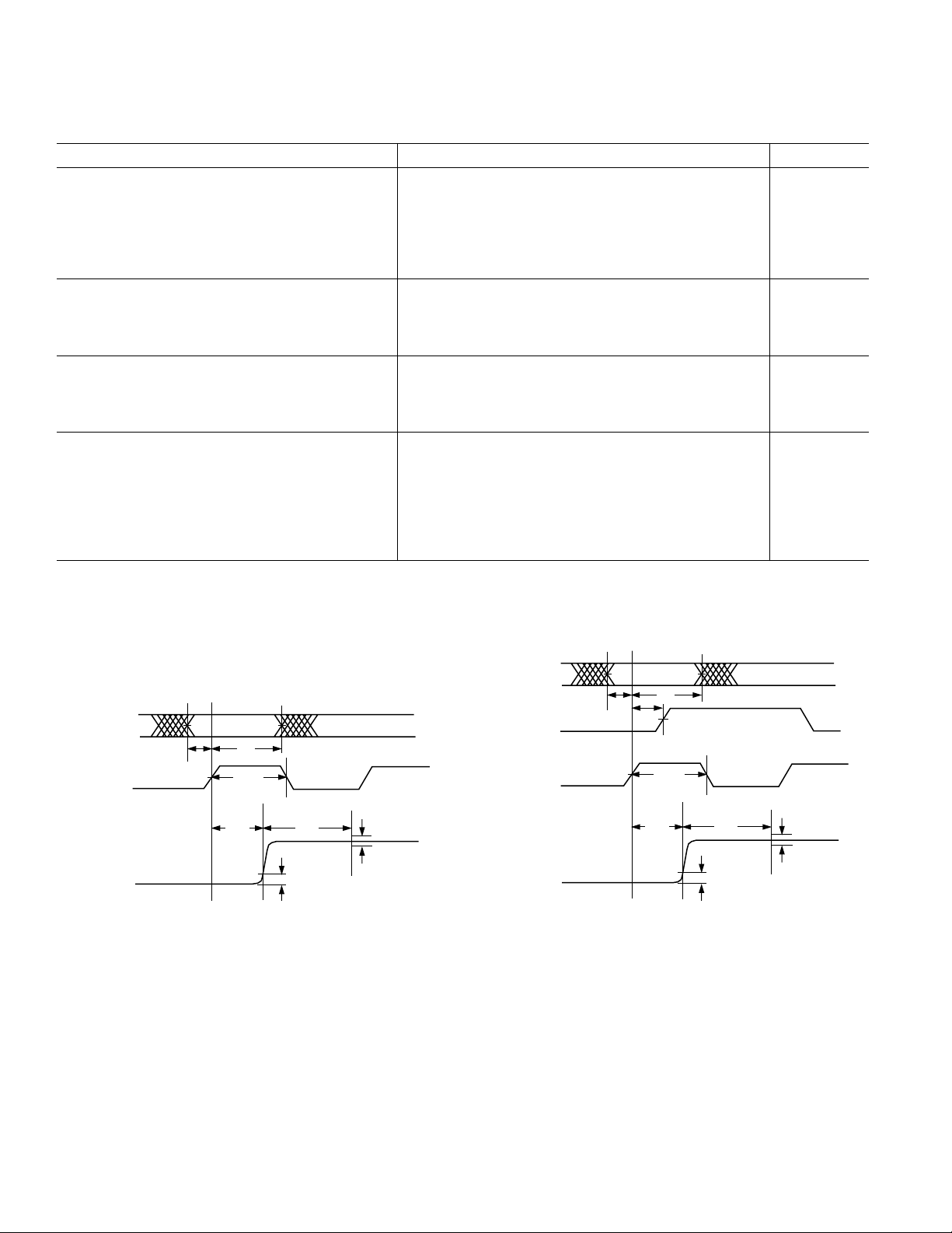
PLL CLOCK ENABLED—FIGURE 1a
Input Setup Time (tS), TA = 25°C 0.5 ns
Input Hold Time (t
Latch Pulsewidth (t
), TA = 25°C 1.0 ns
H
), TA = 25°C 1.5 ns
LPW
PLL CLOCK DISABLED—FIGURE 1b
Input Setup Time (tS), TA = 25°C –1.2 ns
Input Hold Time (t
Latch Pulsewidth (t
CLK/PLLLOCK Delay (t
PLLLOCK (V
), TA = 25°C 3.2 ns
H
), TA = 25°C 1.5 ns
LPW
), TA = 25°C 3.0 V
OH
), TA = 25°C 2.8 3.2 ns
OD
PLLLOCK (VOL), TA = 25°C 0.3 V
*MOD0, MOD1, DIV0, DIV1, SLEEP, RESET have typical input currents of 15 µA.
Specifications subject to change without notice.
= 20 mA, unless
OUTFS
DB0–DB13
t
H
S
t
LPW
t
PD
t
ST
0.025%
0.025%
CLK+ – CLK–
IOUTA
OR
IOUTB
t
Figure 1a. Timing Diagram—PLL Clock Multiplier Enabled
DB0–DB13
t
H
t
OD
t
LPW
t
PD
t
ST
0.025%
0.025%
PLLLOCK
CLK+ – CLK–
IOUTA
OR
IOUTB
t
S
Figure 1b. Timing Diagram—PLL Clock Multiplier Disabled
–4–
REV. A
Page 5
AD9772A
(T
to T
, AVDD = 3.3 V, CLKVDD = 3.3 V, PLLVDD = 0 V, DVDD = 3.3 V, I
MAX
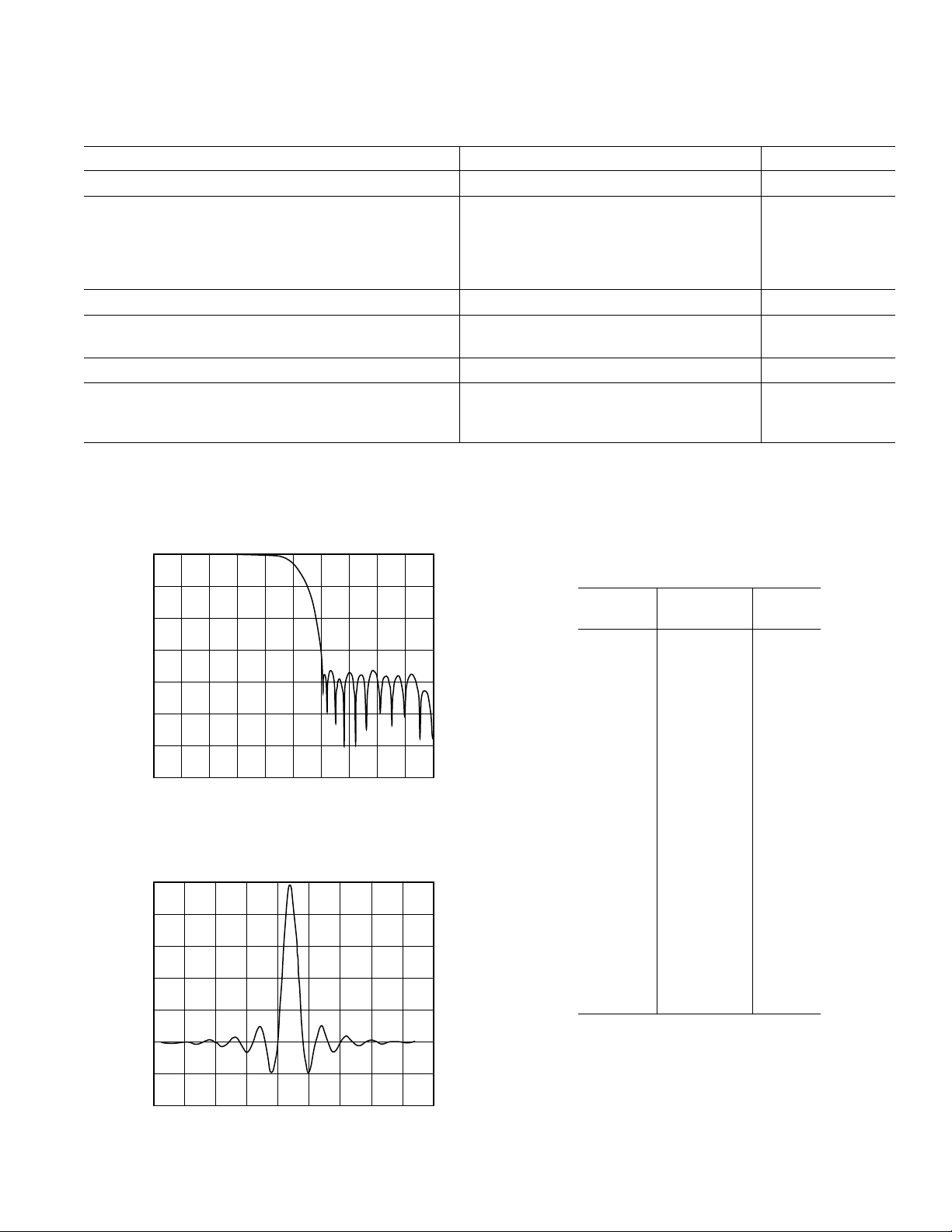
DIGITAL FILTER SPECIFICATIONS
MIN
differential transformer coupled output, 50 doubly terminated, unless otherwise noted.)
Parameter Min Typ Max Unit
MAXIMUM INPUT DATA RATE (f
) 150 MSPS
DATA
DIGITAL FILTER CHARACTERISTICS
Passband Width1: 0.005 dB 0.401 f
Passband Width: 0.01 dB 0.404 f
Passband Width: 0.1 dB 0.422 f
Passband Width: –3 dB 0.479 f
LINEAR PHASE (FIR IMPLEMENTATION)
STOPBAND REJECTION
0.606 f
GROUP DELAY
CLOCK
to 1.394 f
2
CLOCK
73 dB
21 Input Clocks
IMPULSE RESPONSE DURATION
–40 dB 36 Input Clocks
–60 dB 42 Input Clocks
NOTES
1
Excludes sin(x)/x characteristic of DAC.
2
Defined as the number of data clock cycles between impulse input and peak of output response.
Specifications subject to change without notice.
= 20 mA,
OUTFS
OUT/fDATA
OUT/fDATA
OUT/fDATA
OUT/fDATA
0
–20
–40
–60
–80
OUTPUT – dB
–100
–120
–140
0
0.2 0.3 0.4 0.5 0.6 0.7 0.8 0.9
FREQUENCY – DC TO f
DATA
10.1
Figure 2a. FIR Filter Frequency Response—Baseband Mode
1
0.8
0.6
0.4
0.2
Table I. Integer Filter Coefficients for Interpolation Filter
(43-Tap Half-Band FIR Filter)
Lower Upper Integer
Coefficient Coefficient Value
H(1) H(43) 10
H(2) H(42) 0
H(3) H(41) –31
H(4) H(40) 0
H(5) H(39) 69
H(6) H(38) 0
H(7) H(37) –138
H(8) H(36) 0
H(9) H(35) 248
H(10) H(34) 0
H(11) H(33) –419
H(12) H(32) 0
H(13) H(31) 678
H(14) H(30) 0
H(15) H(29) –1083
H(16) H(28) 0
H(17) H(27) 1776
H(18) H(26) 0
H(19) H(25) –3282
H(20) H(24) 0
H(21) H(23) 10364
H(22) 16384
NORMALIZED OUTPUT
0
–0.2
–0.4
0
10 15 20 25 30 35 40 45
5
TIME – Samples
Figure 2b. FIR Filter Impulse Response—Baseband Mode
REV. A
–5–
Page 6
AD9772A
WARNING!
ESD SENSITIVE DEVICE
ABSOLUTE MAXIMUM RATINGS*
Parameter With Respect to Min Max Unit
AVDD, DVDD1-2, CLKVDD, PLLVDD ACOM, DCOM, CLKCOM, PLLCOM –0.3 +4.0 V
AVDD, DVDD1-2, CLKVDD, PLLVDD AVDD, DVDD1-2, CLKVDD, PLLVDD –4.0 +4.0 V
ACOM, DCOM1-2, CLKCOM, PLLCOM ACOM, DCOM1-2, CLKCOM, PLLCOM –0.3 +0.3 V
REFIO, REFLO, FSADJ, SLEEP ACOM –0.3 AVDD + 0.3 V
, I
I
OUTA
OUTB
DB0–DB13, MOD0, MOD1, PLLLOCK DCOM1-2 –0.3 DVDD + 0.3 V
CLK+, CLK– CLKCOM –0.3 CLKVDD + 0.3 V
DIV0, DIV1, RESET CLKCOM –0.3 CLKVDD + 0.3 V
LPF PLLCOM –0.3 PLLVDD + 0.3 V
Junction Temperature 125 °C
Storage Temperature –65 +150 °C
Lead Temperature (10 sec) 300 °C
*Stresses above those listed under Absolute Maximum Ratings may cause permanent damage to the device. This is a stress rating only; functional operation of the device
at these or any other conditions above those indicated in the operational sections of this specification is not implied. Exposure to absolute maximum ratings for extended
periods may affect device reliability.
ACOM –1.0 AVDD + 0.3 V
ORDERING GUIDE
Temperature Package Package
Model Range Description Option*
AD9772AAST –40°C to +85°C 48-Lead LQFP ST-48
THERMAL CHARACTERISTIC
Thermal Resistance
48-Lead LQFP
= 91°C/W
θ
JA
θ
= 28°C/W
JC
AD9772EB Evaluation Board
*ST = Thin Plastic Quad Flatpack.
CAUTION
ESD (electrostatic discharge) sensitive device. Electrostatic charges as high as 4000 V readily
accumulate on the human body and test equipment and can discharge without detection. Although
the AD9772A features proprietary ESD protection circuitry, permanent damage may occur on
devices subjected to high-energy electrostatic discharges. Therefore, proper ESD precautions are
recommended to avoid performance degradation or loss of functionality.
–6–
REV. A
Page 7
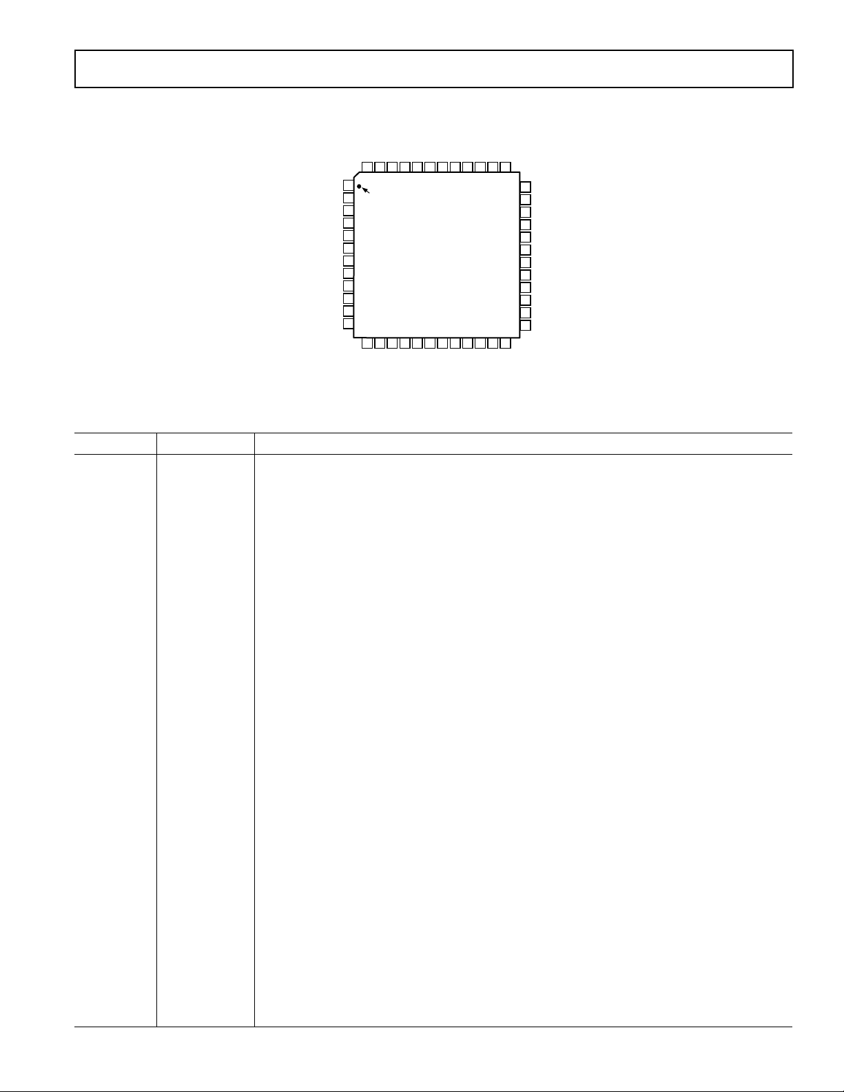
PIN CONFIGURATION
AD9772A
AVDD
AVDD
AD9772A
(Not to Scale)
DB1
(LSB) DB0
OUTAIOUTB
ACOM
I
TOP VIEW
MOD0
MOD1
DCOM
ACOM
FSADJ
DVDD
DCOM
REFIO
REFLO
NC
DVDD
ACOM
NC
36
SLEEP
35
LPF
34
PLLVDD
33
PLLCOM
32
CLKVDD
31
CLKCOM
30
CLK–
29
CLK+
28
DIV0
27
DIV1
26
RESET
25
PLLLOCK
1
DCOM
2
DCOM
DB12
DB11
DB10
DB9
DB8
DB7
DB6
DB5
DB4
3
4
5
6
7
8
9
10
11
12
(MSB) DB13
NC = NO CONNECT
DVDD
DVDD
48 47 46 45 44 39 38 3743 42 41 40
PIN 1
IDENTIFIER
13 14 15 16 17 18 19 20 21 22 23 24
DB3
DB2
PIN FUNCTION DESCRIPTIONS
Pin No. Mnemonic Description
1, 2, 19, 20 DCOM Digital Common
3 DB13 Most Significant Data Bit (MSB)
4–15 DB12–DB1 Data Bits 1–12
16 DB0 Least Significant Data Bit (LSB)
17 MOD0 Invokes digital high-pass filter response (i.e., “half-wave” digital mixing mode). Active High.
18 MOD1 Invokes “Zero-Stuffing” Mode. Active High. Note, “quarter-wave” digital mixing occurs with MOD0
also set HIGH.
23, 24 NC No Connect, Leave Open
21, 22, 47, 48 DVDD Digital Supply Voltage (2.8 V to 3.2 V)
25 PLLLOCK Phase Lock Loop Lock Signal when PLL clock multiplier is enabled. High indicates PLL is locked to
input clock. Provides 1× clock output when PLL clock multiplier is disabled. Maximum fanout is one
(i.e., <10 pF).
26 RESET Resets internal divider by bringing momentarily high when PLL is disabled to synchronize internal
1× clock to the input data and/or multiple AD9772A devices.
27, 28 DIV1, DIV0 DIV1 along with DIV0 sets the PLL’s prescaler divide ratio (refer to Table III.)
29 CLK+ Noninverting Input to Differential Cock. Bias to midsupply (i.e., CLKVDD/2).
30 CLK– Inverting Input to Differential Clock. Bias to midsupply (i.e., CLKVDD/2).
31 CLKCOM Clock Input Common
32 CLKVDD Clock Input Supply Voltage (2.8 V to 3.2 V)
33 PLLCOM Phase Lock Loop Common
34 PLLVDD Phase Lock Loop (PLL) Supply Voltage (3.1 V to 3.5 V). To disable PLL clock multiplier, connect
PLLVDD to PLLCOM.
35 LPF PLL Loop Filter Node. This pin should be left as a no connect (open) unless the DAC update rate is
less than 10 MSPS, in which case a series RC should be connected from LPF to PLLVDD as indicated on
the evaluation board schematic.
36 SLEEP Power-Down Control Input. Active High. Connect to ACOM if not used.
37, 41, 44 ACOM Analog Common
38 REFLO Reference Ground when Internal 1.2 V Reference Used. Connect to AVDD to disable internal reference.
39 REFIO Reference Input/Output. Serves as reference input when internal reference disabled (i.e., tie REFLO
to AVDD). Serves as 1.2 V reference output when internal reference activated (i.e., tie REFLO to
ACOM). Requires 0.1 µF capacitor to ACOM when internal reference activated.
40 FSADJ Full-Scale Current Output Adjust
42 I
43 I
OUTB
OUTA
Complementary DAC Current Output. Full-scale current when all data bits are 0s.
DAC Current Output. Full-scale current when all data bits are 1s.
45, 46 AVDD Analog Supply Voltage (2.8 V to 3.2 V)
REV. A
–7–
Page 8
AD9772A
DEFINITIONS OF SPECIFICATIONS
Linearity Error (Also Called Integral Nonlinearity or INL)
Linearity error is defined as the maximum deviation of the actual
analog output from the ideal output, determined by a straight
line drawn from zero to full scale.
Differential Nonlinearity (or DNL)
DNL is the measure of the variation in analog value, normalized
to full scale, associated with a 1 LSB change in digital input code.
Monotonicity
A D/A converter is monotonic if the output either increases or
remains constant as the digital input increases.
Offset Error
The deviation of the output current from the ideal of zero is
called offset error. For I
inputs are all 0s. For I
, 0 mA output is expected when the
OUTA
, 0 mA output is expected when all
OUTB
inputs are set to 1s.
Gain Error
The difference between the actual and ideal output span. The
actual span is determined by the output when all inputs are set
to 1s, minus the output when all inputs are set to 0s.
Output Compliance Range
The range of allowable voltage at the output of a current-output
DAC. Operation beyond the maximum compliance limits may
cause either output stage saturation or breakdown, resulting in
nonlinear performance.
Temperature Drift
Temperature drift is specified as the maximum change from the
ambient (25°C) value to the value at either T
MIN
or T
MAX
. For
offset and gain drift, the drift is reported in ppm of full-scale
range (FSR) per °C. For reference drift, the drift is reported in
ppm per °C.
Power Supply Rejection
The maximum change in the full-scale output as the supplies
are varied from minimum to maximum specified voltages.
Settling Time
The time required for the output to reach and remain within a
specified error band about its final value, measured from the
start of the output transition.
Glitch Impulse
Asymmetrical switching times in a DAC give rise to undesired
output transients that are quantified by a glitch impulse. It is
specified as the net area of the glitch in pV-s.
Spurious-Free Dynamic Range
The difference, in dB, between the rms amplitude of the output
signal and the peak spurious signal over the specified bandwidth.
Total Harmonic Distortion
THD is the ratio of the rms sum of the first six harmonic components to the rms value of the measured fundamental. It is
expressed as a percentage or in decibels (dB).
Signal-to-Noise Ratio (SNR)
S/N is the ratio of the rms value of the measured output signal
to the rms sum of all other spectral components below the
Nyquist frequency, excluding the first six harmonics and dc.
The value for SNR is expressed in decibels.
Passband
Frequency band in which any input applied therein passes
unattenuated to the DAC output.
Stopband Rejection
The amount of attenuation of a frequency outside the passband
applied to the DAC, relative to a full-scale signal applied at the
DAC input within the passband.
Group Delay
Number of input clocks between an impulse applied at the
device input and peak DAC output current.
Impulse Response
Response of the device to an impulse applied to the input.
Adjacent Channel Power Ratio (or ACPR)
A ratio in dBc between the measured power within a channel
relative to its adjacent channel.
FROM HP8644A
SIGNAL GENERATOR
AWG2021
OR
DG2020
EXT.
CLOCK
1k
1k
DIGITAL
DATA
CLKVDD
CLKCOM
CLK+
CLK–
SLEEP
3.3V
1
EDGE-
TRIGGERED
LATCHES
AD9772A
1/2
INTERPOLATION
CH1
CH2
MOD0
CLOCK DISTRIBUTION
AND MODE SELECT
FILTER
CONTROL
2 FIR
FILTER
CONTROL
3.3V3.3V
HP8130
PULSE GENERATOR
EXT. INPUT
MOD1
RESET
PLLLOCK
MUX
2/4
ZERO
STUFF
MUX
+1.2V REFERENCE
AND CONTROL AMP
REFLOAVDDACOMDVDDDCOM
DIV0
PLLCLOCK
MULTIPLIER
14-BIT DAC
Figure 3. Basic AC Characterization Test Setup
–8–
DIV1
PLLCOM
LPF
PLLVDD
I
OUTA
I
OUTB
REFIO
FSADJ
0.1F
1.91k
50
MINI-CIRCUITS
T1–1T
100
20pF
TO FSEA30
SPECTRUM
ANALYZER
20pF50
REV. A
Page 9
AD9772A
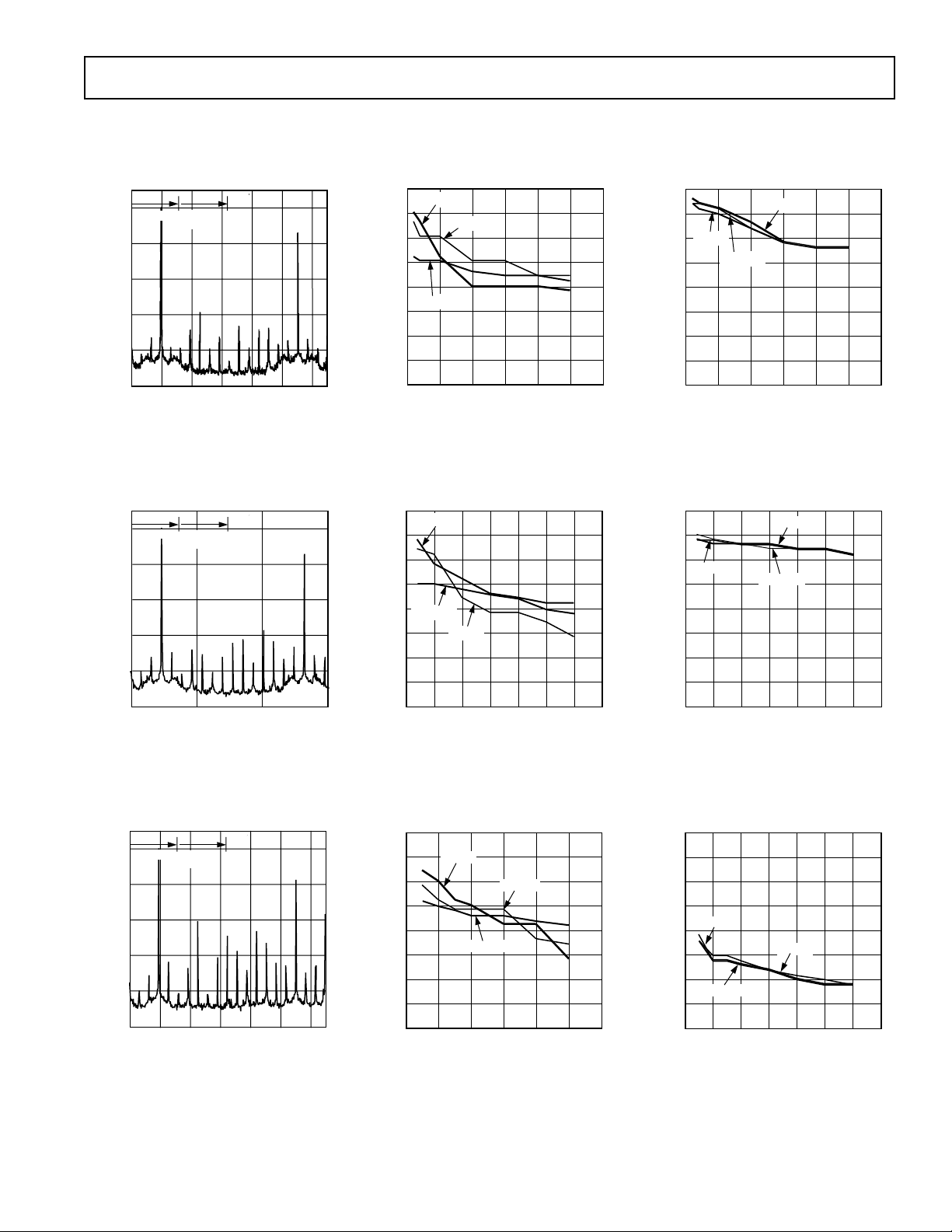
Typical AC Characterization Curves
90
0
–20
–40
–60
AMPLITUDE – dBm
–80
–100
IN-BAND
OUT-OF-
BAND
40 60 80 100
f
– MHz
OUT
120200
TPC 1. Single-Tone Spectral Plot @
f
= 65 MSPS with f
DATA
0
IN-BAND
–20
–40
–60
AMPLITUDE – dBm
–80
–100
OUT-OF-
BAND
50 100
FREQUENCY – MHz
OUT
= f
DATA
/3
TPC 4. Single-Tone Spectral Plot @
f
= 78 MSPS with f
DATA
OUT
= f
DATA
/3
1500
85
80
75
70
SFDR – dBc
65
60
55
50
TPC 2. In-Band SFDR vs. f
@ f
90
85
80
75
70
SFDR – dBc
65
60
55
50
TPC 5. In-Band SFDR vs. f
@ f
(AVDD = 3.3 V, CLKVDD = 3.3 V, PLLVDD = 0 V, DVDD = 3.3 V, I
PLL Disabled.)
0dBFS
–12dBFS
= 65 MSPS
DATA
–6dBFS
–12dBFS
= 78 MSPS
DATA
–6dBFS
0dBFS
f
f
OUT
OUT
– MHz
20 25105
– MHz
OUT
30150
OUT
301502025105
35
70
65
60
0dBFS
55
50
SFDR – dBc
45
40
35
30
–12dBFS
TPC 3. Out-of-Band SFDR vs.
f
@ f
70
65
60
55
50
45
AMPLITUDE – dBm
40
35
30
OUT
DATA
0dBFS
0
5 101520253035
TPC 6. Out-of-Band SFDR vs.
f
@ f
OUT
DATA
OUTFS
–6dBFS
f
– MHz
OUT
= 65 MSPS
–6dBFS
–12dBFS
f
– MHz
OUT
= 78 MSPS
= 20 mA,
20 25105
30150
0
–20
–40
–60
AMPLITUDE – dBm
–80
–100
IN-BAND
OUT-OF-
BAND
100 150 200 250
FREQUENCY – MHz
TPC 7. Single-Tone Spectral Plot
@ f
= 160 MSPS with f
DATA
OUT
= f
REV. A
300500
DATA
/3
90
85
80
75
70
65
AMPLITUDE – dBm
60
55
50
0dBFS
–6dBFS
–12dBFS
0
10 20 30 40 50 60
f
– MHz
OUT
TPC 8. In-Band SFDR vs. f
@ f
= 160 MSPS
DATA
–9–
OUT
70
65
60
55
–6dBFS
50
45
AMPLITUDE – dBm
40
–12dBFS
35
30
0
10 20 30 40 50 60 70
0dBFS
f
– MHz
OUT
TPC 9. Out-of-Band SFDR vs.
f
OUT
@ f
= 160 MSPS
DATA
Page 10
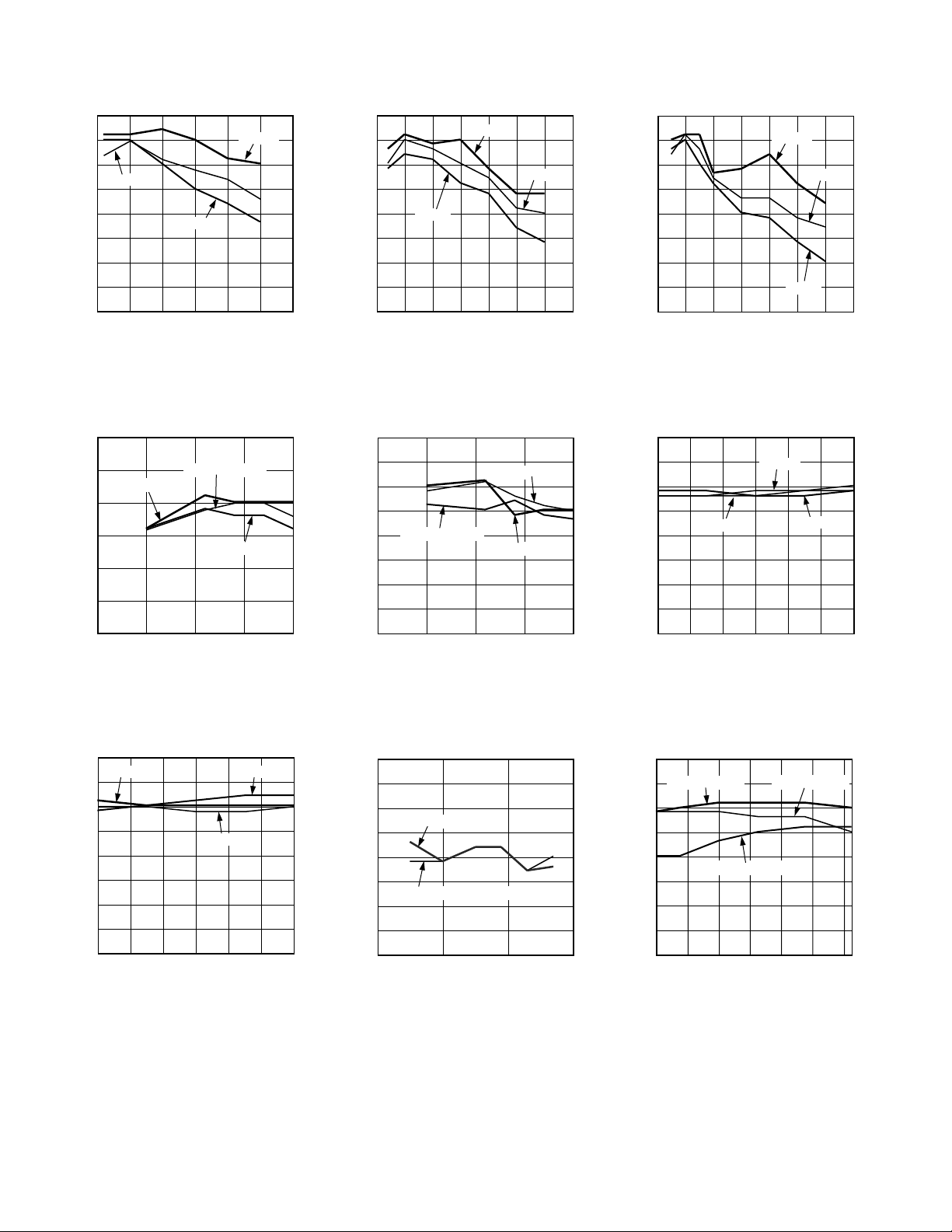
AD9772A
90
85
80
75
70
IMD – dBc
65
60
55
50
–3dBFS
0dBFS
0
51015202530
f
– MHz
OUT
–6dBFS
TPC 10. Third Order IMD Products
vs. f
IMD – dBc
@ f
OUT
90
85
f
DATA
80
75
70
65
60
–20
DATA
= 65MSPS
–15
= 65 MSPS
f
= 160MSPS
DATA
f
= 78MSPS
DATA
–10 –50
A
– dBFS
OUT
TPC 13. Third Order IMD Products
vs. A
OUT
@ f
OUT
= f
DAC
/11
90
85
80
75
70
IMD – dBc
65
60
55
50
0dBFS
0
5 1015202530
f
OUT
–6dBFS
–3dBFS
– MHz
TPC 11. Third Order IMD Products
vs. f
IMD – dBc
90
85
80
75
70
65
60
55
50
OUT
–20
@ f
f
DATA
DATA
–15
= 160MSPS
= 78 MSPS
f
= 78MSPS
DATA
f
= 65MSPS
DATA
–10 –50
A
– dBFS
OUT
TPC 14. Third Order IMD Products
vs. A
OUT
@ f
OUT
= f
DAC
/5
90
f
OUT
–6dBFS
–3dBFS
0dBFS
– MHz
85
80
75
70
IMD – dBc
65
60
55
35
50
0
10 20 30 40 50 60 70
TPC 12. Third Order IMD Products
90
85
80
75
70
SFDR – dBc
65
60
55
50
OUT
@ f
vs. f
TPC 15. SFDR vs. AVDD @ f
10 MHz, f
= 160 MSPS
DATA
–3dBFS
0dBFS
3.1 3.2 3.4 3.5
AVDD – Volts
= 320 MSPS
DAC
–6dBFS
OUT
3.63.33.0
=
90
85
80
75
70
IMD – dBc
65
60
55
50
0dBFS
3.1 3.2 3.4 3.5
AVDD – Volts
–3dBFS
–6dBFS
TPC 16. Third Order IMD Products
vs. AVDD @ f
= 10 MHz, f
OUT
DAC
=
320 MSPS
3.63.33.0
TPC 17. SNR vs. f
90
85
SNR – dBc
80
75
70
65
60
55
50
PLL OFF
PLL ON, OPTIMUM DIV0/1 SETTINGS
25
75
f
DAC
DAC
–10–
125 175
– MHz
@ f
OUT
= 10 MHz
90
f
DATA
= 65MSPS
SFDR – dBc
55
50
85
80
75
70
65
60
–40
f
= 78MSPS
DATA
TEMPERATURE – C
f
DATA
080–20
= 160MSPS
20 40 60
TPC 18. In-Band SFDR vs. Temperature @ f
OUT
= f
DATA
/11
REV. A
Page 11

AD9772A
FUNCTIONAL DESCRIPTION
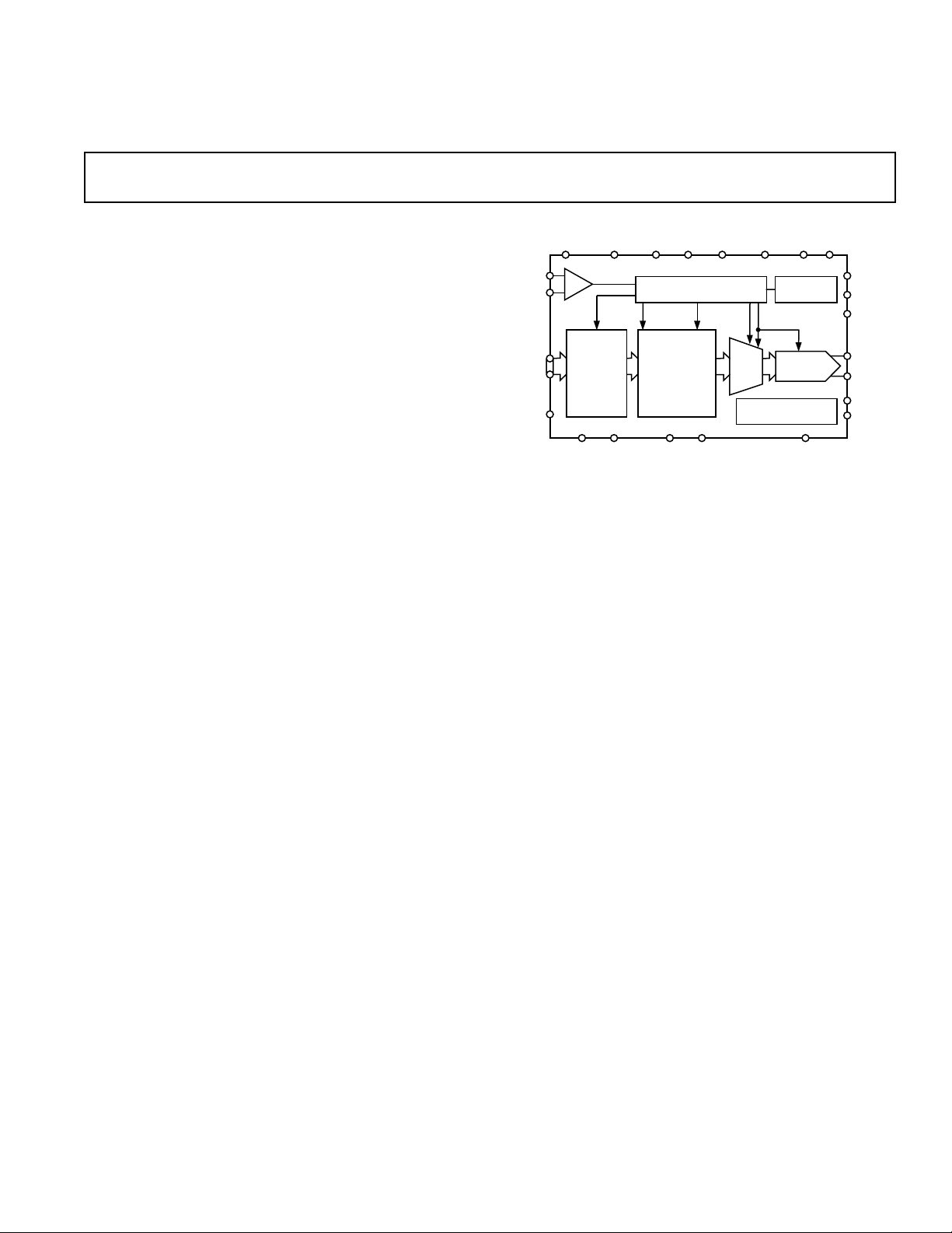
Figure 4 shows a simplified block diagram of the AD9772A.
The AD9772A is a complete, 2⫻ oversampling, 14-bit DAC that
includes a 2⫻ interpolation filter, a phase-locked loop (PLL)
clock multiplier and a 1.20 V bandgap voltage reference. While
the AD9772A’s digital interface can support input data rates as
high as 160 MSPS, its internal DAC can operate up to 400 MSPS,
thus providing direct IF conversion capabilities. The 14-bit DAC
provides two complementary current outputs whose full-scale
current is determined by an external resistor. The AD9772A
features a flexible, low jitter, differential clock input providing
excellent noise rejection while accepting a sine wave input. An
on-chip PLL clock multiplier produces all of the necessary
synchronized clocks from an external reference clock source.
Separate supply inputs are provided for each functional block to
ensure optimum noise and distortion performance. A SLEEP
mode is also included for power savings.
DIV1
DIV0
PLL CLOCK
MULTIPLIER
14-BIT DAC
REFLO
PLLCOM
LPF
PLLVDD
I
OUTA
I
OUTB
REFIO
FSADJ
CLK+
CLK–
DATA
INPUTS
(DB13...
DB0)
SLEEP
CLKCOM
CLKVDD MOD0 MOD1 RESET
AD9772A
CLOCK DISTRIBUTION
AND MODE SELECT
1/2
1
CONTROL
EDGE-
TRIGGERED
LATCHES
DCOM DVDD ACOM AVDD
POLATION
FILTER
2 FIR
INTER-
FILTER
PLLLOCK
MUX
CONTROL
ZERO
STUFF
MUX
AND CONTROL AMP
2/4
+1.2V REFERENCE
Figure 4. Functional Block Diagram
Preceding the 14-bit DAC is a 2⫻ digital interpolation filter that
can be configured for a low-pass (i.e., baseband mode) or highpass (i.e., direct IF mode) response. The input data is latched
into the edge-triggered input latches on the rising edge of the
differential input clock as shown in Figure 1a and then interpolated by a factor of two by the digital filter. For traditional baseband
applications, the 2⫻ interpolation filter has a low-pass response.
For direct IF applications, the filter’s response can be converted
into a high-pass response to extract the higher image. The output
data of the 2⫻ interpolation filter can update the 14-bit DAC
directly or undergo a “zero-stuffing” process to increase the DAC
update rate by another factor of two. This action enhances the
relative signal level and passband flatness of the higher images.
DIGITAL MODES OF OPERATION
The AD9772A features four different digital modes of operation
controlled by the digital inputs, MOD0 and MOD1. MOD0
controls the 2⫻ digital filter’s response (i.e., low-pass or high-
pass), while MOD1 controls the “zero-stuffing” option. The
selected mode as shown in Table II will depend on whether the
application requires the reconstruction of a baseband or IF signal.
Table II. Digital Modes
Digital Digital ZeroMode MOD0 MOD1 Filter Stuffing
Baseband 0 0 Low No
Baseband 0 1 Low Yes
Direct IF 1 0 High No
Direct IF 1 1 High Yes
Applications requiring the highest dynamic range over a wide
bandwidth should consider operating the AD9772A in a baseband
mode. Note, the “zero-stuffing” option can also be used in this
mode although the ratio of signal to image power will be reduced.
Applications requiring the synthesis of IF signals should consider operating the AD9772A in a Direct IF mode. In this case,
the “zero-stuffing” option should be considered when synthesizing and selecting IFs beyond the input data rate, f
reconstructed IF falls below f
, the “zero-stuffing” option
DATA
DATA
. If the
may or may not be beneficial. Note, the dynamic range (i.e.,
SNR/SFDR) is also optimized by disabling the PLL Clock Multiplier (i.e., PLLVDD to PLLCOM) and using an external low
jitter clock source operating at the DAC update rate, f
DAC
.
2 Interpolation Filter Description
The 2⫻ interpolation filter is based on a 43-tap half-band sym-
metric FIR topology that can be configured for a low- or
high-pass response, depending on the state of the MOD0
control input. The low-pass response is selected with MOD0
LOW while the high-pass response is selected with MOD0
HIGH. The low-pass frequency and impulse response of the
half-band interpolation filter are shown in Figures 2a and 2b,
while Table I lists the idealized filter coefficients. Note, a FIR
filter’s impulse response is also represented by its idealized
filter coefficients.
The 2× interpolation filter essentially multiplies the input data
rate to the DAC by a factor of two, relative to its original input
data rate, while simultaneously reducing the magnitude of the
first image associated with the original input data rate occurring
at f
DATA
– f
FUNDAMENTAL
. Note, as a result of the 2⫻ interpolation, the digital filter’s frequency response is uniquely defined
over its Nyquist zone of dc to f
, with mirror images occur-
DATA
ring in adjacent Nyquist zones.
The benefits of an interpolation filter are clearly seen in Figure 5, which shows an example of the frequency and time
domain representation of a discrete time sine wave signal before
and after it is applied to the 2⫻ digital interpolation filter in a
low-pass configuration. Images of the sine wave signal appear
around multiples of the DAC’s input data rate (i.e., f
DATA
) as
predicted by sampling theory. These undesirable images will
also appear at the output of a reconstruction DAC, although
attenuated by the DAC’s sin(x)/x roll-off response.
In many bandlimited applications, the images from the reconstruction process must be suppressed by an analog filter following
the DAC. The complexity of this analog filter is typically determined by the proximity of the desired fundamental to the first
image and the required amount of image suppression. Adding to
the complexity of this analog filter may be the requirement of
compensating for the DAC’s sin(x)/x response.
REV. A
–11–
Page 12

AD9772A
Referring to Figure 5, the “new” first image associated with the
DAC’s higher data rate after interpolation is “pushed” out further relative to the input signal, since it now occurs at 2 ⫻
f
DATA
– f
FUNDAMENTAL
. The “old” first image associated with the
lower DAC data rate before interpolation is suppressed by the
digital filter. As a result, the transition band for the analog
reconstruction filter is increased, thus reducing the complexity of the
analog filter. Furthermore, the sin(x)/x roll-off over the original
input data passband (i.e., dc to f
/2) is significantly reduced.
DATA
As previously mentioned, the 2⫻ interpolation filter can be
converted into a high-pass response, thus suppressing the “fundamental” while passing the “original” first image occurring at
f
DATA
– f
FUNDAMENTAL
. Figure 6 shows the time and frequency
representation for a high-pass response of a discrete time sine
wave. This action can also be modeled as a “1/2 wave” digital
mixing process in which the impulse response of the low-pass
filter is digitally mixed with a square wave having a frequency
TIME
DOMAIN
1/ f
DATA
f
FUNDAMENTAL
FREQUENCY
DOMAIN
ST
1
f
DATA
INPUT DATA
LATCH
IMAGE
f
FUNDAMENTAL
2f
DATA
SUPPRESSED
1STIMAGE
2 INTERPOLATION
of exactly f
/2. Since the even coefficients have a zero value
DATA
(refer to Table I), this process simplifies into inverting the center coefficient of the low-pass filter (i.e., invert H(18)). Note
that this also corresponds to inverting the peak of the impulse
response shown in Figure 2a. The resulting high-pass frequency
response becomes the frequency inverted mirror image of the
low-pass filter response shown in Figure 2b.
It is worth noting that the “new” first image now occurs at f
f
FUNDAMENTAL
exists for image selection, thus mandating that the f
. A reduced transition region of 2 ⫻ f
FUNDAMENTAL
FUNDAMENTAL
DATA
be placed sufficiently high for practical filtering purposes in direct
IF applications. Also, the “lower sideband images” occurring at
f
– f
DATA
f
FUNDAMENTAL
FUNDAMENTAL
) experience a frequency inversion while the “upper
sideband images” occurring at f
tiples (i.e., N ⫻ f
1/ 2f
DATA
FILTER
2
1
2f
ST
NEW
DATA
IMAGE
DIGITAL
FILTER
RESPONSE
f
DATA
and its multiples (i.e., N ⫻ f
+ f
DATA
+ f
FUNDAMENTAL
DAC'S SIN (X)/X
RESPONSE
f
DATA
DAC
DATA
2f
FUNDAMENTAL
) do not.
DATA
–
DATA
and its mul-
+
f
DATA
2
f
DATA
Figure 5. Time and Frequency Domain Example of Low-Pass 2⫻ Digital Interpolation Filter
1/ 2f
f
DATA
2
FILTER
2
f
DATA
DATA
RESPONSE
2f
DIGITAL
FILTER
DATA
DAC'S SIN (X)/X
RESPONSE
f
f
2
DATA
DATA
DAC
TIME
DOMAIN
f
FUNDAMENTAL
FREQUENCY
DOMAIN
1/ f
DATA
INPUT DATA
LATCH
f
DATA
f
DATA
ST
1
IMAGE
2f
DATA
LOWER IMAGE
SUPPRESSED
f
FUNDAMENTAL
2 INTERPOLATION
UPPER AND
Figure 6. Time and Frequency Domain Example of High-Pass 2⫻ Digital Interpolation Filter
–12–
REV. A
Page 13

AD9772A
“Zero Stuffing” Option Description
As shown in Figure 7, a “zero” or null in the frequency responses
(after interpolation and DAC reconstruction) occurs at the final
DAC update rate (i.e., 2 ⫻ f
) due to the DAC’s inherent
DATA
sin(x)/x roll-off response. In baseband applications, this roll-off
in the frequency response may not be as problematic since much
of the desired signal energy remains below f
DATA
/2 and the
amplitude variation is not as severe. However, in direct IF
applications interested in extracting an image above f
DATA
/2,
this roll-off may be problematic due to the increased passband
amplitude variation as well as the reduced signal level of the
higher images.
0
WITH
–10
–20
dBFS
–30
–40
0
BASEBAND
“ZERO-STUFFING”
REGION
WITHOUT
FREQUENCY –
“ZERO-STUFFING”
f
DATA
40.5 1 1.5 2 2.5 3 3.5
Figure 7. Effects of “Zero-Stuffing” on DAC’s
Sin(x)/x Response
For instance, if the digital data into the AD9772A represented a
baseband signal centered around f
/10, the reconstructed baseband signal out of the AD9772A
f
DATA
/4 with a passband of
DATA
would experience only a 0.18 dB amplitude variation over its
passband with the “first image” occurring at 7/4 f
DATA
with 17 dB
of attenuation relative to the fundamental. However, if the highpass filter response was selected, the AD9772A would now
produce pairs of images at [(2N + 1) ⫻ f
DATA
] ± f
/4 where N
DATA
= 0, 1 . . .. Note, due to the DAC’s sin(x)/x response, only the
lower or upper sideband images centered around f
DATA
may
be useful although they would be attenuated by –2.1 dB and
–6.54 dB respectively, as well as experience a passband amplitude
roll-off of 0.6 dB and 1.3 dB.
To improve upon the passband flatness of the desired image
and/or to extract higher images (i.e., 3 ⫻ f
DATA
± f
FUNDAMENTAL
)
the “zero-stuffing” option should be employed by bringing the
MOD1 pin HIGH. This option increases the effective DAC
update rate by another factor of two since a “midscale” sample
(i.e., 10 0000 0000 0000) is inserted after every data sample
originating from the 2⫻ interpolation filter. A digital multiplexer
switching at a rate of 4 ⫻ f
between the interpolation filter’s
DATA
output and a data register containing the “midscale” data sample is
used to implement this option as shown in Figure 6. Hence, the
DAC output is now forced to return to its differential midscale
current value (i.e., I
OUTA–IOUTB
≅ 0 mA) after reconstructing
each data sample from the digital filter.
The net effect is to increase the DAC update rate such that the
“zero” in the sin(x)/x frequency response now occurs at 4 ⫻ f
DATA
along with a corresponding reduction in output power as shown
REV. A
–13–
in Figure 7. Note that if the 2⫻ interpolation filter’s high-pass
response is also selected, this action can be modeled as a “1/4
wave” digital mixing process since this is equivalent to digitally
mixing the impulse response of the low-pass filter with a square
wave having a frequency of exactly f
DATA
(i.e., f
DAC
/4).
It is important to realize that the “zero stuffing” option by itself
does not change the location of the images but rather their signal
level, amplitude flatness and relative weighting. For instance, in
the previous example, the passband amplitude flatness of the
lower and upper sideband images centered around f
DATA
are
improved to 0.14 dB and 0.24 dB respectively, while the signal
level has changed to –6.5 dBFS and –7.5 dBFS. The lower or
upper sideband image centered around 3 ⫻ f
will exhibit an
DATA
amplitude flatness of 0.77 dB and 1.29 dB with signal levels of
approximately –14.3 dBFS and –19.2 dBFS.
PLL CLOCK MULTIPLIER OPERATION
The Phase Lock Loop (PLL) clock multiplier circuitry along
with the clock distribution circuitry can produce the necessary
internally synchronized 1⫻, 2⫻, and 4⫻ clocks for the edge
triggered latches, 2⫻ interpolation filter, “zero stuffing” multi-
plier, and DAC. Figure 8 shows a functional block diagram of
the PLL clock multiplier, which consists of a phase detector, a
charge pump, a voltage controlled oscillator (VCO), a prescaler,
and digital control inputs/outputs. The clock distribution
circuitry generates all the internal clocks for a given mode of
operation. The charge pump and VCO are powered from
PLLVDD while the differential clock input buffer, phase detector,
prescaler and clock distribution circuitry are powered from
CLKVDD. To ensure optimum phase noise performance from
the PLL clock multiplier and clock distribution circuitry,
PLLVDD and CLKVDD must originate from the same clean
analog supply.
CLK+
CLK–
PLLLOCK
CLKVDD
OUT1
CLKCOM
CLOCK
DISTRIBUTION
MOD1
MOD0
RESET
–+
PHASE
DETECTOR
EXT/INT
CLOCK CONTROL
PRESCALER
DIV1
DIV0
AD9772A
CHARGE
PUMP
VCO
LPF
PLL
VDD
PLL
COM
DNC
2.7V TO
3.6V
Figure 8. Clock Multiplier with PLL Clock
Multiplier Enabled
The PLL clock multiplier has two modes of operation. It can be
enabled for less demanding applications providing a reference
clock meeting the minimum specified input data rate of 6 MSPS.
It can be disabled for applications below this data rate or for
applications requiring higher phase noise performance. In this
case, a reference clock at twice the input data rate (i.e., 2 ⫻ f
DATA
)
must be provided without the “zero stuffing” option selected
and four times the input data rate (i.e., 4 ⫻ f
DATA
) with the
“zero stuffing” option selected. Note, multiple AD9772A devices
Page 14

AD9772A
can be synchronized in either mode if driven by the same
reference clock, since the PLL clock multiplier when enabled
ensures synchronization. RESET can be used for synchronization if the PLL clock multiplier is disabled.
Figure 8 shows the proper configuration used to enable the PLL
clock multiplier. In this case, the external clock source is applied
to CLK+ (and/or CLK–) and the PLL clock multiplier is fully
enabled by connecting PLLVDD to CLKVDD.
The settling/acquisition time characteristics of the PLL are also
dependent on the divide-by-N ratio as well as the input data rate.
In general, the acquisition time increases with increasing data rate
(for fixed divide-by-N ratio) or increasing divide-by-N ratio (for
fixed input data rate).
Since the VCO can operate over a 96 MHz–400 MHz range,
the prescaler divide-by-ratio following the VCO must be set
according to Table III for a given input data rate (i.e., f
DATA
)
to ensure optimum phase noise and successful “locking.” In
general, the best phase noise performance for any prescaler
setting is achieved with the VCO operating near its maximum
output frequency of 400 MHz. Note, the divide-by-N ratio also
depends on whether the “zero stuffing” option is enabled since
this option requires the DAC to operate at four times the input
data rate. The divide-by-N ratio is set by DIV1 and DIV0.
With the PLL clock multiplier enabled, PLLLOCK serves as an
active HIGH control output which may be monitored upon system power-up to indicate that the PLL is successfully “locked” to
the input clock. Note, when the PLL clock multiplier is NOT
locked, PLLLOCK will toggle between logic HIGH and LOW
in an asynchronous manner until locking is finally achieved.
As a result, it is recommended that PLLLOCK, if monitored,
be sampled several times to detect proper locking 100 ms
upon power-up.
Table III. Recommended Prescaler Divide-by-N Ratio Settings
f
DATA
Divide-by-N
(MSPS) MOD1 DIV1 DIV0 Ratio
48–1600001
24–1000012
12–500104
6–250118
24–1001001
12–501012
6–251104
3–12.5 1 1 1 8
As stated earlier, applications requiring input data rates below
6 MSPS must disable the PLL clock multiplier and provide an
external reference clock. However, applications already containing a low phase noise (i.e., jitter) reference clock that is twice
(or four times) the input data rate should consider disabling the
PLL clock multiplier to achieve the best SNR performance from
the AD9772A. Note that the SFDR performance and wideband
noise performance of the AD9772A remains unaffected with or
without the PLL clock multiplier enabled.
The effects of phase noise on the AD9772A’s SNR performance
becomes more noticeable at higher reconstructed output frequencies and signal levels. Figure 9 compares the phase noise
of a full-scale sine wave at exactly f
/4 at different data rates
DATA
(hence carrier frequency) with the optimum DIV1, DIV0 setting.
The effects of phase noise, and its effect on a signal’s CNR
performance, becomes even more evident at higher IF frequencies as shown in Figure 10. In both instances, it is the
“narrowband” phase noise that limits the CNR performance.
0
–10
–20
–30
–40
–50
–60
–70
–80
NOISE DENSITY – dBm/Hz
–90
–100
–110
PLL ON, f
PLL OFF, f
0
= 160MSPS
DATA
PLL ON, f
DATA
PLL ON, f
PLL ON, f
= 50MSPS
DATA
12
FREQUENCY OFFSET – MHz
= 100MSPS
= 75MSPS
DATA
DATA
3
= 50MSPS
4
5
Figure 9. Phase Noise of PLL Clock Multiplier at Exactly
= f
f
OUT
/4 at Different f
DATA
Settings with Optimum
DATA
DIV0/DIV1 Settings Using R & S FSEA30, RBW = 30 kHz
10
–10
–30
–50
–70
AMPLITUDE – dBm
–90
–110
120
122 124 126 128 130
FREQUENCY – MHz
Figure 10. Direct IF Mode Reveals Phase Noise Degradation with and without PLL Clock Multiplier (IF = 125 MHz
and f
= 100 MSPS)
DATA
To disable the PLL Clock Multiplier, connect PLLVDD to
PLLCOM as shown in Figure 11. LPF may remain open since
this portion of the PLL circuitry is now disabled. The differential clock input should be driven with a reference clock twice the
data input rate in baseband applications and four times the data
input rate in direct IF applications in which the “1/4 wave”
mixing option is employed (i.e., MOD1 and MOD0 active
HIGH). The clock distribution circuitry remains enabled providing a 1⫻ internal clock at PLLLOCK. Digital input data is
–14–
REV. A
Page 15

AD9772A
latched into the AD9772 on every other rising edge of the differential clock input. The rising edge that corresponds to the input
latch immediately precedes the rising edge of the 1⫻ clock at
PLLLOCK. Adequate setup and hold time for the input data as
shown in Figure 1b should be allowed. Note that enough delay
is present between CLK+/CLK– and the data input latch to
cause the minimum setup time for input data to be negative.
This is noted in the Digital Specifications section. PLLLOCK
contains a relatively weak driver output, with its output delay
) sensitive to output capacitance loading. Thus PLLLOCK
(t
OD
should be buffered for fanouts greater than one, and/or load
capacitance greater than 10 pF. If a data timing issue exists
between the AD9772A and its external driver device, the 1⫻
clock appearing at PLLLOCK can be inverted via an external
gate to ensure proper setup and hold time.
CLK+
CLK–
PLLLOCK
CLKVDD
OUT1
CLOCK
DISTRIBUTION
–+
PHASE
DETECTOR
EXT/INT
CLOCK CONTROL
PRESCALER
AD9772A
CHARGE
PUMP
VCO
PLL
COM
LPF
PLL
VDD
DIGITAL DATA IN
EXTERNAL
2 CLK
DELAYED INTERNAL
LOAD DEPENDENT
DELAYED 1 CLK
1 CLK
AT PLLLOCK
I
OR I
OUTA
OUTB
DATA
t
LPW
t
D
t
PD
DATA ENTERS INPUT
LATCHES ON THIS EDGE
t
PD
Figure 12. Internal Timing of AD9772A with PLL Disabled
Figure 13 illustrates the details of the RESET function timing.
RESET going from a high to a low logic level enables the 1⫻
clock output, generated by the PLLLOCK pin. If RESET goes
low at a time well before the rising edge of the 2⫻ clock, then
PLLLOCK will go high on the following edge of the 2⫻ clock. If
RESET goes from a high to a low logic level 600 ps or later
following the rising edge of the 2× clock, there will be a delay of
one 2⫻ clock cycle before PLLLOCK goes high. In either case,
as long as RESET remains low, PLLLOCK will change state on
every rising edge of the 2⫻ clock. As stated before, it is the rising
edge of the 2⫻ clock which immediately precedes the rising edge
of PLLLOCK that latches data into the AD9772A input latches.
CLKCOM
RESET
MOD1
MOD0
DIV1
DIV0
Figure 11. Clock Multiplier with PLL Clock Multiplier
Disabled
SYNCHRONIZATION OF CLK/DATA USING RESET WITH PLL DISABLED
The relationship between the internal and external clocks in this
mode is shown in Figure 12. A clock at the output update data
rate (2⫻ the input data rate) must be applied to the CLK inputs. Internal dividers create the internal 1⫻ clock necessary for
the input latches. With the PLL disabled, a delayed version of the
1⫻ clock is present at the PLLLOCK pin. The DAC latch is
updated on the particular rising edge of the external 2⫻ clock
which corresponds to the rising edge of the 1⫻ clock. Updates
to the input data should be synchronized to this specific rising
edge as shown in Figure 12. To ensure this synchronization, a
Logic 1 should be momentarily applied to the RESET pin on
power up, before CLK is applied. Applying a momentary Logic 1
to RESET brings the 1⫻ clock at PLLLOCK to a Logic 1. On
the next rising edge of the 2⫻ clock, the 1⫻ clock will go to
Logic 0. The following rising edge of the 2⫻ clock will cause
the 1⫻ clock to Logic 1 again, as well as update the data in
both of the input latches.
.
CH1 2.00V CH2 2.00V M 10.0ns CH3 2.00V
[ T ]
T
1
T
2
T
3
CH1 2.00V CH2 2.00V M 10.0ns CH4 1.20V
CH3 2.00V
a.
b.
Figure 13. RESET Timing of AD9772A with PLL Disabled
REV. A
–15–
Page 16

AD9772A
DAC OPERATION
The 14-bit DAC along with the 1.2 V reference and reference
control amplifier is shown in Figure 14. The DAC consists of a
large PMOS current source array capable of providing up to
20 mA of full-scale current, I
. The array is divided into
OUTFS
thirty-one equal currents that make up the five most significant
bits (MSBs). The next four bits, or middle bits, consist of 15
equal current sources whose values are 1/16th of an MSB
current source. The remaining LSBs are binary weighted fractions of the middle-bits’ current sources. All of these current
sources are switched to one or the other of two output nodes
(i.e., I
OUTA
or I
) via PMOS differential current switches.
OUTB
Implementing the middle and lower bits with current sources,
instead of an R-2R ladder, enhances its dynamic performance
for multitone or low amplitude signals and helps maintain the
DAC’s high output impedance.
2.7V TO 3.6V
R
2k
0.1F
SET
REFLO AVDD
+1.2V REF
REFIO
FSADJ
I
REF
SEGMENTED
SWITCHES
AD9772A
250pF
SWITCHES
INTERPOLATED
DIGITAL DATA
CURRENT
SOURCE
ARRAY
LSB
ACOM
I
OUTA
I
OUTB
I
OUTA
I
OUTB
V
= V
OUTA
R
LOAD
– V
OUTB
DIFF
R
LOAD
Figure 14. Block Diagram of Internal DAC, 1.2 V
Reference, and Reference Control Circuits
The full-scale output current is regulated by the reference control
amplifier and can be set from 2 mA to 20 mA via an external
resistor, R
, as shown in Figure 14. R
SET
, in combination
SET
with both the reference control amplifier and voltage reference,
REFIO, sets the reference current, I
, which is mirrored to
REF
the segmented current sources with the proper scaling factor.
The full-scale current, I
value of I
REF
.
, is exactly thirty-two times the
OUTFS
DAC TRANSFER FUNCTION
The AD9772A provides complementary current outputs, I
and I
I
OUTFS
I
OUTB
current output appearing at I
both the input code and I
. I
OUTB
will provide a near full-scale current output,
OUTA
, when all bits are high (i.e., DAC CODE = 16383) while
, the complementary output, provides no current. The
OUTA
and can be expressed as:
OUTFS
I
= (DAC CODE/16384) × I
OUTA
I
= (16383 – DAC CODE)/16384 × I
OUTB
and I
is a function of
OUTB
OUTFS
OUTFS
OUTA
(1)
(2)
where DAC CODE = 0 to 16383 (i.e., Decimal Representation).
As previously mentioned, I
current I
V
REFIO
I
, which is nominally set by a reference voltage
REF
, and external resistor, R
= 32 × I
OUTFS
REF
is a function of the reference
OUTFS
. It can be expressed as:
SET
(3)
where
I
REF
= V
REFIO/RSET
(4)
The two current outputs will typically drive a resistive load
directly or via a transformer. If dc coupling is required, I
and I
loads, R
that R
I
OUTA
should be directly connected to matching resistive
OUTB
, that are tied to analog common, ACOM. Note
LOAD
may represent the equivalent load resistance seen by
LOAD
or I
as would be the case in a doubly terminated 50 Ω
OUTB
OUTA
or 75 Ω cable. The single-ended voltage output appearing at the
and I
I
OUTA
V
= I
OUTA
V
= I
OUTB
Note that the full-scale value of V
nodes is simply:
OUTB
× R
OUTA
OUTB
× R
LOAD
LOAD
OUTA
and V
should not
OUTB
(5)
(6)
exceed the specified output compliance range of 1.25 V to prevent signal compression. To maintain optimum distortion and
; V
OUTA
OUTA
DIFF
and
and
(7)
can be
linearity performance, the maximum voltages at V
V
should not exceed ±500 mV p-p.
OUTB
The differential voltage, V
I
, is:
OUTB
V
DIFF
= (I
OUTA
– I
OUTB
Substituting the values of I
, appearing across I
DIFF
) × R
LOAD
, I
OUTB
and I
OUTA
REF
expressed as:
V
= [(2 DAC CODE – 16383)/16384] ×
DIFF
(32 R
LOAD/RSET
) × V
REFIO
(8)
The last two equations highlight some of the advantages of
operating the AD9772A differentially. First, the differential
operation will help cancel common-mode error sources such as
noise, distortion and dc offsets associated with I
OUTA
and I
OUTB
.
Second, the differential code-dependent current and subsequent
voltage, V
output (i.e., V
, is twice the value of the single-ended voltage
DIFF
OUTA
or V
), thus providing twice the signal
OUTB
power to the load.
Note that the gain drift temperature performance for a singleended (V
OUTA
and V
) or differential output (V
OUTB
DIFF
) of the
AD9772A can be enhanced by selecting temperature tracking
resistors for R
LOAD
and R
due to their ratiometric relation-
SET
ship as shown in Equation 8.
REFERENCE OPERATION
The AD9772A contains an internal 1.20 V bandgap reference
that can easily be disabled and overridden by an external
reference. REFIO serves as either an output or input, depending
on whether the internal or external reference is selected. If
REFLO is tied to ACOM, as shown in Figure 15, the internal
reference is activated, and REFIO provides a 1.20 V output. In
this case, the internal reference must be compensated externally
with a ceramic chip capacitor of 0.1 µF or greater from REFIO
to REFLO. If any additional loading is required, REFIO should
be buffered with an external amplifier having an input bias current less than 100 nA.
–16–
REV. A
Page 17

AD9772A
250pF
2.7V TO 3.6V
CURRENT
SOURCE
ARRAY
ADDITIONAL
LOAD
OPTIONAL
EXTERNAL
REF BUFFER
REFLO AVDD
+1.2V REF
REFIO
0.1F
FSADJ
2k
AD9772A
Figure 15. Internal Reference Configuration
The internal reference can be disabled by connecting REFLO to
AVDD. In this case, an external 1.2 V reference such as the
AD1580 may then be applied to REFIO as shown in Figure 16.
The external reference may provide either a fixed reference
voltage to enhance accuracy and drift performance or a varying
reference voltage for gain control. Note that the 0.1 µF compensation capacitor is not required since the internal reference is
disabled, and the high input impedance of REFIO minimizes
any loading of the external reference.
2.7V TO 3.6V
REFLO AVDD
+1.2V REF
REFIO
FSADJ
AD9772A
250pF
REFERENCE
CONTROL
AMPLIFIER
CURRENT
SOURCE
ARRAY
AD1580
10k
V
REFIO
I
=
REF
R
SET
V
REFIO/RSET
Figure 16. External Reference Configuration
REFERENCE CONTROL AMPLIFIER
The AD9772A also contains an internal control amplifier that is
used to regulate the DAC’s full-scale output current, I
OUTFS
.
The control amplifier is configured as a V-I converter, as shown
in Figure 16, such that its current output, I
the ratio of the V
Equation 4. I
REF
the proper scaling factor to set I
and an external resistor, R
REFIO
is copied to the segmented current sources with
as stated in Equation 3.
OUTFS
, is determined by
REF
, as stated in
SET
The control amplifier allows a wide (10:1) adjustment span of
I
over a 2 mA to 20 mA range by setting I
OUTFS
62.5 µA and 625 µA. The wide adjustment span of I
between
REF
OUTFS
provides several application benefits. The first benefit relates
directly to the power dissipation of the AD9772’s DAC, which
is proportional to I
(refer to the Power Dissipation sec-
OUTFS
tion). The second benefit relates to the 20 dB adjustment, which
is useful for system gain control purposes.
I
can be controlled using the single-supply circuit shown in
REF
Figure 17 for a fixed R
. In this example, the internal refer-
SET
ence is disabled, and the voltage of REFIO is varied over its
compliance range of 1.25 V to 0.10 V. REFIO can be driven
by a single-supply DAC or digital potentiometer, thus allowing
to be digitally controlled for a fixed R
I
REF
. This particular
SET
example shows the AD5220, an 8-bit serial input digital potentiometer, along with the AD1580 voltage reference. Note, since
the input impedance of REFIO does interact and load the
digital potentiometer wiper to create a slight nonlinearity in the
programmable voltage divider ratio, a digital potentiometer with
10 kΩ or less of resistance is recommended.
2.7V TO 3.6V
REFLO AVDD
+1.2V REF
REFIO
FSADJ
AD9772A
SET
250pF
CURRENT
SOURCE
ARRAY
1.2V
AD1580
10k
AD5220
10k
R
Figure 17. Single-Supply Gain Control Circuit
ANALOG OUTPUTS
The AD9772A produces two complementary current outputs,
and I
I
OUTA
differential operation. I
complementary single-ended voltage outputs, V
, via a load resistor, R
V
OUTB
, which may be configured for single-ended or
OUTB
OUTA
and I
LOAD
can be converted into
OUTB
, as described in the DAC
OUTA
and
Transfer Function section, by Equations 5 through 8. The
differential voltage, V
, existing between V
DIFF
OUTA
and V
OUTB
,
can also be converted to a single-ended voltage via a transformer
or differential amplifier configuration.
Figure 18 shows the equivalent analog output circuit of the
AD9772A, consisting of a parallel combination of PMOS differential current switches associated with each segmented current
source. The output impedance of I
OUTA
and I
is determined
OUTB
by the equivalent parallel combination of the PMOS switches
and is typically 200 kΩ in parallel with 3 pF. Due to the nature
of a PMOS device, the output impedance is also slightly dependent
on the output voltage (i.e., V
OUTA
and V
) and, to a lesser
OUTB
extent, the analog supply voltage, AVDD, and full-scale current,
. Although the output impedance’s signal dependency can
I
OUTFS
be a source of dc nonlinearity and ac linearity (i.e., distortion), its
effects can be limited if certain precautions are noted.
I
OUTA
and I
also have a negative and positive voltage compli-
OUTB
ance range. The negative output compliance range of –1.0 V is
set by the breakdown limits of the CMOS process. Operation
beyond this maximum limit may result in a breakdown of the
output stage and affect the reliability of the AD9772A. The positive
output compliance range is slightly dependent on the full-scale
output current, I
. Operation beyond the positive compliance
OUTFS
range will induce clipping of the output signal, which severely
degrades the AD9772A’s linearity and distortion performance.
AVDD
AD9772A
I
R
OUTA
LOAD
I
OUTB
R
LOAD
Figure 18. Equivalent Analog Output Circuit
REV. A
–17–
Page 18

AD9772A
Operating the AD9772A with reduced voltage output swings at
I
OUTA
and I
in a differential or single-ended output configu-
OUTB
ration reduces the signal dependency of its output impedance,
thus enhancing distortion performance. Although the voltage
compliance range of I
OUTA
and I
extends from –1.0 V to
OUTB
+1.25 V, optimum distortion performance is achieved when the
maximum full-scale signal at I
OUTA
and I
does not exceed
OUTB
approximately 0.5 V. A properly selected transformer with a
grounded center-tap will allow the AD9772A to provide the
required power and voltage levels to different loads while maintaining reduced voltage swings at I
OUTA
and I
. DC-coupled
OUTB
applications requiring a differential or single-ended output configuration should size R
accordingly. Refer to Applying the
LOAD
AD9772A section for examples of various output configurations.
The most significant improvement in the AD9772A’s distortion
and noise performance is realized using a differential output
configuration. The common-mode error sources of both I
I
can be substantially reduced by the common-mode rejection
OUTB
OUTA
and
of a transformer or differential amplifier. These commonmode error sources include even-order distortion products
and noise. The enhancement in distortion performance becomes
more significant as the reconstructed waveform’s frequency
content increases and/or its amplitude decreases. The distortion and noise performance of the AD9772A is also dependent
on the full-scale current setting, I
OUTFS
. Although I
set between 2 mA and 20 mA, selecting an I
OUTFS
can be
OUTFS
of 20 mA will
provide the best distortion and noise performance.
In summary, the AD9772A achieves the optimum distortion
and noise performance under the following conditions:
1. Positive voltage swing at I
OUTA
and I
limited to 0.5 V.
OUTB
2. Differential Operation.
3. I
set to 20 mA.
OUTFS
4. PLL Clock Multiplier Disabled
Note the majority of the AC Characterization Curves for the
AD9772A are performed under the above-mentioned operating
conditions.
DIGITAL INPUTS/OUTPUTS
The AD9772A consists of several digital input pins used for
data, clock, and control purposes. It also contains a single digital output pin, PLLLOCK, used to monitor the status of the
internal PLL clock multiplier or provide a 1⫻ clock output. The
14-bit parallel data inputs follow standard positive binary coding
where DB13 is the most significant bit (MSB), and DB0 is the
least significant bit (LSB). I
current when all data bits are at Logic 1. I
produces a full-scale output
OUTA
OUTB
produces a
complementary output with the full-scale current split between
the two outputs as a function of the input code.
The digital interface is implemented using an edge-triggered
master slave latch and is designed to support an input data rate
as high as 160 MSPS. The clock can be operated at any duty
cycle that meets the specified latch pulsewidth as shown in
Figures 1a and 1b. The setup and hold times can also be varied
within the clock cycle as long as the specified minimum times
are met. The digital inputs (excluding CLK+ and CLK–) are
CMOS-compatible with its logic thresholds, V
THRESHOLD,
set to
approximately half the digital positive supply (i.e., DVDD or
CLKVDD) or
V
THRESHOLD
= DVDD/2 (±20%)
The internal digital circuitry of the AD9772A is capable of operating over a digital supply range of 2.8 V to 3.2 V. As a result, the
digital inputs can also accommodate TTL levels when DVDD is
set to accommodate the maximum high level voltage of the TTL
drivers V
. Although a DVDD of 3.3 V will typically ensure
OH(MAX)
proper compatibility with most TTL logic families, a series
200 Ω resistors are recommended between the TTL logic driver
and digital inputs to limit the peak current through the ESD protection diodes if V
exceeds DVDD by more than 300 mV.
OH(MAX)
Figure 19 shows the equivalent digital input circuit for the data
and control inputs.
DVDD
DIGITAL
INPUT
Figure 19. Equivalent Digital Input
The AD9772A features a flexible differential clock input operating from separate supplies (i.e., CLKVDD, CLKCOM) to
achieve optimum jitter performance. The two clock inputs,
CLK+ and CLK–, can be driven from a single-ended or differential clock source. For single-ended operation, CLK+ should be
driven by a single-ended logic source while CLK– should be set
to the logic source’s threshold voltage via a resistor divider/capacitor network referenced to CLKVDD as shown in Figure 20. For
differential operation, both CLK+ and CLK– should be biased to
CLKVDD/2 via a resistor divider network as shown in Figure 21.
An RF transformer as shown in Figure 3 can also be used to
convert a single-ended clock input to a differential clock input.
AD9772A
R
V
THRESHOLD
1k
1k
SERIES
0.1F
CLK+
CLKVDD
CLK–
CLKCOM
Figure 20. Single-Ended Clock Interface
–18–
REV. A
Page 19

RATIO –
f
OUT
/
f
DATA
100
90
40
0.0
DVDD – mA
80
70
60
50
0.1 0.2 0.3 0.4 0.5
30
20
10
0
f
DATA
= 160MSPS
f
DATA
= 125MSPS
f
DATA
= 100MSPS
f
DATA
= 65MSPS
f
DATA
= 50MSPS
f
DATA
= 25MSPS
AD9772A
AD9772A
0.1F
ECL/PECL
0.1F
0.1F
Figure 21. Differential Clock Interface
The quality of the clock and data input signals are important in
achieving the optimum performance. The external clock driver
circuitry should provide the AD9772A with a low jitter clock
input which meets the min/max logic levels while providing fast
edges. Although fast clock edges help minimize any jitter that
will manifest itself as phase noise on a reconstructed waveform,
the high gain-bandwidth product of the AD9772A’s differential
comparator can tolerate sine wave inputs as low as 0.5 V p-p,
with minimal degradation in its output noise floor.
Digital signal paths should be kept short and run lengths
matched to avoid propagation delay mismatch. The insertion of
a low- value resistor network (i.e., 50 Ω to 200 Ω) between the
AD9772A digital inputs and driver outputs may be helpful in
reducing any overshooting and ringing at the digital inputs that
contribute to data feedthrough.
SLEEP MODE OPERATION
The AD9772A has a SLEEP function that turns off the output
current and reduces the analog supply current to less than 6 mA
over the specified supply range of 2.8 V to 3.2 V. This mode
can be activated by applying a Logic Level 1 to the SLEEP
pin. The AD9772A takes less than 50 ns to power down and
approximately 15 µs to power back up.
POWER DISSIPATION
The power dissipation, PD, of the AD9772A is dependent on
several factors, including:
1. AVDD, PLLVDD, CLKVDD, and DVDD, the power supply voltages.
2. I
3. f
, the full-scale current output.
OUTFS
, the update rate.
DATA
4. the reconstructed digital input waveform.
The power dissipation is directly proportional to the analog
supply current, I
I
is directly proportional to I
AVDD
to f
Conversely, I
waveform and f
full-scale sine wave output ratios (f
rates with DVDD = 3 V. The supply current from CLKVDD
and PLLVDD is relatively insensitive to the digital input waveform, but shown directly proportional to the update rate as
shown in Figure 23.
REV. A
DATA
.
DVDD
, and the digital supply current, I
AVDD
is dependent on both the digital input
. Figure 22 shows I
DATA
1k
CLK+
1k
CLKVDD
1k
CLK–
1k
CLKCOM
and is insensitive
OUTFS,
DVDD
OUT/fDATA
) for various update
.
DVDD
as a function of
Figure 22. I
25
20
15
I – mA
10
5
0
0
Figure 23. I
vs. Ratio @ DVDD = 3.3 V
DVDD
I
CLKVDD
I
PLLVDD
50 100 150 200
f
– MSPS
DATA
PLLVDD
and I
CLKVDD
vs. f
DATA
APPLYING THE AD9772A OUTPUT CONFIGURATIONS
The following sections illustrate some typical output configurations for the AD9772A. Unless otherwise noted, it is assumed
that I
is set to a nominal 20 mA for optimum performance.
OUTFS
For applications requiring the optimum dynamic performance,
a differential output configuration is highly recommended. A
differential output configuration may consist of either an RF
transformer or a differential op amp configuration. The transformer configuration provides the optimum high-frequency
performance and is recommended for any application allowing
for ac coupling. The differential op amp configuration is suitable
for applications requiring dc coupling, a bipolar output, signal
gain, and/or level-shifting.
A single-ended output is suitable for applications requiring a
unipolar voltage output. A positive unipolar output voltage will
result if I
load resistor, R
OUTA
and/or I
, referred to ACOM. This configuration may
LOAD
is connected to an appropriately-sized
OUTB
be more suitable for a single-supply system requiring a dc-coupled,
ground-referred output voltage. Alternatively, an amplifier could
be configured as an I-V converter, thus converting I
I
into a negative unipolar voltage. This configuration pro-
OUTB
vides the best dc linearity since I
OUTA
or I
is maintained at
OUTB
OUTA
or
a virtual ground.
–19–
Page 20

AD9772A
DIFFERENTIAL COUPLING USING A TRANSFORMER
An RF transformer can be used to perform a differential-tosingle-ended signal conversion as shown in Figure 24. A
differentially-coupled transformer output provides the optimum
distortion performance for output signals whose spectral content
lies within the transformer’s passband. An RF transformer such
as the Mini-Circuits T1-1T provides excellent rejection of
common-mode distortion (i.e., even-order harmonics) and noise
over a wide frequency range. It also provides electrical isolation
and the ability to deliver twice the power to the load. Transformers with different impedance ratios may also be used for
impedance matching purposes. Note that the transformer
provides ac coupling only and its linearity performance degrades
at the low end of its frequency range due to core saturation.
AD9772A
I
OUTA
I
OUTB
OPTIONAL
R
DIFF
MINI-CIRCUITS
T1-1T
R
LOAD
Figure 24. Differential Output Using a Transformer
The center tap on the primary side of the transformer must be
connected to ACOM to provide the necessary dc current path
for both I
at I
OUTA
OUTA
and I
and I
OUTB
. The complementary voltages appearing
OUTB
(i.e., V
OUTA
and V
) swing symmetrically
OUTB
around ACOM and should be maintained with the specified
output compliance range of the AD9772A. A differential resistor, R
of the transformer is connected to the load, R
passive reconstruction filter or cable. R
, may be inserted in applications in which the output
DIFF
is determined by the
DIFF
LOAD
, via a
transformer’s impedance ratio and provides the proper source
termination that results in a low VSWR (Voltage Standing Wave
Ratio). Note that approximately half the signal power will be dissipated across R
DIFF
.
DIFFERENTIAL COUPLING USING AN OP AMP
An op amp can also be used to perform a differential-to-singleended conversion as shown in Figure 25. The AD9772A is
configured with two equal load resistors, R
differential voltage developed across I
OUTA
and I
, of 25 Ω. The
LOAD
is converted
OUTB
to a single-ended signal via the differential op amp configuration. An optional capacitor can be installed across I
I
, forming a real pole in a low-pass filter. The addition of
OUTB
OUTA
and
this capacitor also enhances the op amp’s distortion performance
by preventing the DAC’s high slewing output from overloading
the op amp’s input.
AD9772A
I
OUTA
I
OUTB
25
225
225
C
OPT
25
500
AD8055
500
Figure 25. DC Differential Coupling Using an Op Amp
The common-mode rejection of this configuration is typically
determined by the resistor matching. In this circuit, the differential op amp circuit using the AD8055 is configured to provide
some additional signal gain. The op amp must operate from a
dual supply since its output is approximately ±1.0 V. A high-speed
amplifier, capable of preserving the differential performance of
the AD9772A while meeting other system level objectives (i.e.,
cost, power), should be selected. The op amp’s differential gain,
its gain setting resistor values and full-scale output swing capabilities should all be considered when optimizing this circuit.
The differential circuit shown in Figure 26 provides the necessary level shifting required in a single-supply system. In this
case, AVDD, the positive analog supply for both the AD9772A
and the op amp, is also used to level-shift the differential output
of the AD9772A to midsupply (i.e., AVDD/2). The AD8057 is
a suitable op amp for this application.
AD8057
1k
500
1k
AVDD
AD9772A
I
OUTA
I
OUTB
C
OPT
25 25
225
225
Figure 26. Single-Supply DC Differential Coupled Circuit
SINGLE-ENDED UNBUFFERED VOLTAGE OUTPUT
Figure 27 shows the AD9772A configured to provide a unipolar
output range of approximately 0 V to 0.5 V for a doubly terminated 50 Ω cable since the nominal full-scale current, I
20 mA flows through the equivalent R
R
represents the equivalent load resistance seen by I
LOAD
The unused output (I
directly. Different values of I
) should be connected to ACOM
OUTB
OUTFS
and R
of 25 Ω. In this case,
LOAD
can be selected as
LOAD
OUTFS
OUTA
, of
.
long as the positive compliance range is adhered to. One additional consideration in this mode is the integral nonlinearity
(INL) as discussed in the Analog Output section of this data
sheet. For optimum INL performance, the single-ended, buffered voltage output configuration is suggested.
AD9772A
I
OUTA
I
OUTB
I
OUTFS
= 20mA
50 50
V
OUTA
= 0V TO 0.5V
Figure 27. 0 V to 0.5 V Unbuffered Voltage Output
SINGLE-ENDED BUFFERED VOLTAGE OUTPUT
Figure 28 shows a buffered single-ended output configuration
in which the op amp U1 performs an I-V conversion on the
AD9772A output current. U1 maintains I
OUTA
(or I
OUTB
) at
virtual ground, thus minimizing the nonlinear output impedance
effect on the DAC’s INL performance as discussed in the Analog
Output section. Although this single-ended configuration typically provides the best dc linearity performance, its ac distortion
performance at higher DAC update rates is often limited by
U1’s slewing capabilities. U1 provides a negative unipolar output
voltage and its full-scale output voltage is simply the product of
–20–
REV. A
Page 21

AD9772A
RFB and I
voltage output swing capabilities by scaling I
. The full-scale output should be set within U1’s
OUTFS
OUTFS
and/or RFB.
An improvement in ac distortion performance may result with a
reduced I
since the signal current U1 will be required to
OUTFS
sink will be subsequently reduced.
C
OPT
R
FB
AD9772A
I
OUTA
I
OUTB
I
OUTFS
= 10mA
200
200
U1
V
OUT
= –I
OUTFS
R
FB
Figure 28. Unipolar Buffered Voltage Output
POWER AND GROUNDING CONSIDERATIONS
The AD9772A contains the five following power supply inputs:
AVDD, DVDD1, DVDD2, CLKVDD and PLLVDD. The
AD9772A is specified to operate over a 2.8 V to 3.2 V supply
range, thus accommodating 3.0 V and/or 3.3 V power supplies
with up to ±10% regulation. However, the following two conditions must be adhered to when selecting power supply sources
for AVDD, DVDD1–DVDD2, CLKVDD, and PLLVDD:
1. PLLVDD = CLKVDD = 3.1 V–3.5 V when PLL Clock
Multiplier enabled. (Otherwise PLLVDD = PLLCOM)
2. DVDD1–DVDD2 = CLKVDD ± 0.30 V
To meet the first condition, PLLVDD must be driven by the
same power source as CLKVDD with each supply input independently decoupled with a 0.1 µF capacitor to its respective
grounds. To meet the second condition, CLKVDD can share
the power supply source as DVDD1–DVDD2, using the
decoupling network shown in Figure 29 to isolate digital noise
from the sensitive CLKVDD (and PLLVDD) supply. Alternatively, separate precision voltage regulators can be used to
ensure that condition two is met.
In systems seeking to simultaneously achieve high speed and
high performance, the implementation and construction of the
printed circuit board design is often as important as the circuit
design. Proper RF techniques must be used in device selection,
placement and routing and supply bypassing and grounding.
Figures 37–44 illustrate the recommended printed circuit board
ground, power and signal plane layouts that are implemented on
the AD9772A evaluation board.
Proper grounding and decoupling should be a primary objective
in any high speed, high resolution system. The AD9772A features separate analog and digital supply and ground pins to
optimize the management of analog and digital ground currents
in a system. AVDD, CLKVDD, and PLLVDD must be powered
from a clean analog supply and decoupled to their respective
analog common (i.e., ACOM, CLKCOM and PLLCOM) as
close to the chip as physically possible. Similarly, DVDD1 and
DVDD2, the digital supplies, should be decoupled to DCOM.
For those applications requiring a single 3.3 V supply for both
the analog, digital supply and Phase Lock Loop supply, a clean
AVDD and/or CLKVDD may be generated using the circuit
shown in Figure 29. The circuit consists of a differential LC filter
with separate power supply and return lines. Lower noise can be
attained using low ESR-type electrolytic and tantalum capacitors.
FERRITE
TTL/CMOS
LOGIC
CIRCUITS
3.0V OR 3.3V
POWER SUPPLY
BEADS
+
100F
ELECTROLYTIC
–
+
10F–22F
TANTALUM
–
0.1F
CERAMIC
AVDD
ACOM
Figure 29. Differential LC Filter for 3 V or 3.3 V
Maintaining low noise on power supplies and ground is critical
to obtain optimum results from the AD9772A. If properly
implemented, ground planes can perform a host of functions on
high-speed circuit boards: bypassing, shielding current transport, etc. In mixed-signal design, the analog and digital portions
of the board should be distinct from each other, with the analog
ground plane confined to the areas covering the analog signal
traces, and the digital ground plane confined to areas covering
the digital interconnects.
All analog ground pins of the DAC, reference, and other analog
components should be tied directly to the analog ground plane.
The two ground planes should be connected by a path 1/8 to
1/4 inch wide underneath or within 1/2 inch of the DAC to
maintain optimum performance. Care should be taken to ensure
that the ground plane is uninterrupted over crucial signal paths.
On the digital side, this includes the digital input lines running
to the DAC. On the analog side, this includes the DAC output
signal, reference signal and the supply feeders.
The use of wide runs or planes in the routing of power lines is
also recommended. This serves the dual role of providing a low
series impedance power supply to the part, as well as providing
some “free” capacitive decoupling to the appropriate ground
plane. It is essential that care be taken in the layout of signal and
power ground interconnects to avoid inducing extraneous voltage drops in the signal ground paths. It is recommended that all
connections be short, direct and as physically close to the package as possible in order to minimize the sharing of conduction
paths between different currents. When runs exceed an inch in
length, strip line techniques with proper termination resistors
should be considered. The necessity and value of these resistors
will be dependent upon the logic family used.
For a more detailed discussion of the implementation and construction of high-speed, mixed-signal printed circuit boards,
refer to Analog Devices’ application note AN-333.
REV. A
–21–
Page 22

AD9772A
APPLICATIONS
MULTICARRIER
The AD9772A’s wide dynamic range performance makes it well
suited for next generation base station applications in which it
reconstructs multiple modulated carriers over a designated
frequency band. Cellular multicarrier and multimode radios are
often referred to as software radios since the carrier tuning and
modulation scheme is software programmable and performed
digitally. The AD9772A is the recommended TxDAC in
Analog Device’s SoftCell chipset which comprises the AD6622,
Quadrature Digital Upconverter IC, along with its companion Rx Digital Downconverter IC, the AD6624, and 14-bit,
65 MSPS ADC, the AD6644. Figure 30 shows a generic software radio Tx signal chain based on the AD9772A/AD6622.
Figure 31 shows a spectral plot of the AD9772A operating at
64.54 MSPS reconstructing eight IS-136 modulated carriers
spread over a 25 MHz band. For this particular test scenario,
the AD9772A exhibited 74 dBc SFDR performance along with
a carrier-to-noise ratio (CNR) of 73 dB. Figure 32 shows a spectral
plot of the AD9772A operating at 52 MSPS reconstructing four
equal GSM carriers spread over a 15 MHz band. The SFDR
and CNR (in 100 kHz BW) measured to be 76 dBc and 83.4 dB
respectively along with a channel power of –13.5 dBFS. Note,
the test vectors were generated using Rohde & Schwarz’s
WinIQSIM software.
AD6622
SPORT RCF
SPORT RCF
SPORT RCF
SPORT RCF
JTAG
CIC
FILTER
CIC
FILTER
CIC
FILTER
CIC
FILTER
NCO
QAM
NCO
QAM
NCO
QAM
NCO
QAM
PORT
SUMMATION
CLK
PLLLOCK CLK
AD9772A
OTHER AD6622s FOR
INCREASED CHANNEL
CAPACITY
Figure 30. Generic Multicarrier Signal Chain Using the
AD6622 and AD9772A
–20
–30
–40
–50
–60
–70
AMPLITUDE – dBm
–80
–90
–100
5101520 3025
0
FREQUENCY – MHz
Figure 31. Spectral Plot of AD9772A Reconstructing
Eight IS-136 Modulated Carriers @ f
= 64.54 MSPS,
DATA
PLLVDD = 0
–10
–20
–30
–40
–50
–60
–70
AMPLITUDE – dBm
–80
–90
–100
–110
0
5
10 15
FREQUENCY – MHz
20 25
Figure 32. Spectral Plot of AD9772A Reconstructing
Four GSM Modulated Carriers @ f
= 52 MSPS,
DATA
PLLVDD = 0
Although the above IS-136 and GSM spectral plots are representative of the AD9772A’s performance for a particular set of
test conditions, the following recommendations are offered to
maximize the performance and system integration of the AD9772A
into multicarrier applications:
1. To achieve the highest possible CNR, the PLL Clock Multiplier should be disabled (i.e., PLLVDD to PLLCOM) and
the AD9772A’s clock input driven with a low jitter/phase
noise clock source at twice the input data rate. In this case,
the divide-by-two clock appearing at PLLLOCK should
serve as the master clock for the digital upconverter IC(s)
such as the AD6622. PLLLOCK should be limited to a
fanout of one.
2. The AD9772A achieves its optimum noise and distortion
performance when configured for baseband operation along
with a differential output and a full-scale current, I
OUTFS
,
set to approximately 20 mA.
3. Although the 2⫻ interpolation filters frequency roll-off provides a maximum reconstruction bandwidth of 0.422 ⫻ f
DATA,
the optimum adjacent image rejection (due to the interpolation process) is achieved (i.e., > 73 dBc) if the maximum
channel assignment is kept below 0.400 ⫻ f
DATA.
4. To simplify the subsequent IF stages filter requirements (i.e.,
mixer image and LO rejection), it is often advantageous to
offset the frequency band from dc to relax the transition band
requirements of the IF filter.
5. Oversampling the frequency band often results in improved
SFDR and CNR performance. This implies that the data
input rate to the AD9772A is greater than f
where f
PASSBAND
is the maximum bandwidth in which the
PASSBAND
/0.4
AD9772A will be required to reconstruct and place carriers.
The improved noise performance results in a reduction in
the TxDAC’s noise spectral density due to the added process
gain realized with oversampling. Also, higher oversampling
ratios provide greater flexibility in the frequency planning.
–22–
REV. A
Page 23

AD9772A
BASEBAND SINGLE-CARRIER
The AD9772A is also well suited for wideband single-carrier
applications such as WCDMA and multilevel QAM whose
modulation scheme requires wide dynamic range from the
reconstruction DAC to achieve the out-of-band spectral mask as
well as the in-band CNR performance. Many of these applications strategically place the carrier frequency at one quarter of
the DAC’s input data rate (i.e., f
/4) to simplify the digital
DATA
modulator design. Since this constitutes the first fixed IF frequency, the frequency tuning is accomplished at a later IF stage.
To enhance the modulation accuracy as well as reduce the shape
factor of the second IF SAW filter, many applications will often
specify the passband of the IF SAW filter be greater than the
channel bandwidth. The trade-off is that the TxDAC must now
meet the particular application’s spectral mask requirements
within the extended passband of the 2nd IF, which may include
two or more adjacent channels.
Figure 33 shows a spectral plot of the AD9772A reconstructing
a test vector similar to those encountered in WCDMA applications with the following exception. WCDMA applications
prescribe a root raised cosine filter with an alpha = 0.22, which
limits the theoretical ACPR of the TxDAC to about 70 dB. This
particular test vector represents white noise that has been bandlimited by a “brickwall” bandpass filter with the same passband
such that its maximum ACPR performance is theoretically
83 dB and its peak-to-rms ratio is 12.4 dB. As Figure 33 reveals,
the AD9772A is capable of approximately 78 dB ACPR performance when one accounts for the additive noise/distortion
contributed by the FSEA30 spectrum analyzer.
–30
–40
–50
–60
–70
–80
dBm
–90
–100
–110
–120
–130
C11
CENTER 16.25MHz SPAN 6MHz600kHz
C0 C0
C11
Cu1 Cu1
Figure 33. AD9772A Achieves 78 dB ACPR Performance
Reconstructing a “WCDMA-Like” Test Vector with f
DATA
=
65.536 MSPS and PLLVDD = 0
DIRECT IF
As discussed in the Digital Modes of Operation section, the
AD9772A can be configured to transform digital data representing baseband signals into IF signals appearing at odd multiples
of the input data rate (i.e., N ⫻ f
where N = 1, 3, . . .). This
DATA
is accomplished by configuring the MOD1 and MOD0 digital
inputs HIGH. Note, the maximum DAC update rate of 400 MSPS
limits the data input rate in this mode to 100 MSPS when the
“zero-stuffing operation” is enabled (i.e., MOD1 High). Applications requiring higher IFs (i.e., 140 MHz) using higher data
rates should disable the “zeros-stuffing” operation. Also, to
minimize the effects of the PLL Clock Multipliers phase noise
as shown in Figure 9, an external low jitter/phase noise clock
source equal to 4× f
is recommended.
DATA
Figure 34 shows the actual output spectrum of the AD9772A
reconstructing a 16-QAM test vector with a symbol rate of
5 MSPS. The particular test vector was centered at f
= 100 MSPS, and f
f
DATA
tions, the pair of images appearing around f
= 400 MHz. For many applica-
DAC
DATA
/4 with
DATA
will be more
attractive since they have the flattest passband and highest signal
power. Higher images can also be used with the understanding
that these images will have reduced passband flatness, dynamic
range, and signal power, thus reducing the CNR and ACP performance. Figure 35 shows a dual tone SFDR amplitude sweep
at the various IF images with f
400 MHz and the two tones centered around f
= 100 MSPS and f
DATA
DATA
=
DAC
/4. Note,
since an IF filter is assumed to precede the AD9772A, the
SFDR was measured over a 25 MHz window around the images
occurring at 75 MHz, 125 MHz, 275 MHz, and 325 MHz.
Regardless of what image is selected for a given application, the
adjacent images must be sufficiently filtered. In most cases, a
SAW filter providing differential inputs represents the optimum
device for this purpose. For single-ended SAW filters, a balancedto-unbalanced RF transformer is recommended. The AD9772A’s
high output impedance provides a certain amount of flexibility
in selecting the optimum resistive load, R
, as well as any
LOAD
matching network.
–20
–30
–40
–50
–60
–70
AMPLITUDE – dBm
–80
–90
–100
0
100
FREQUENCY – MHz
200
300
400
Figure 34. Spectral Plot of 16-QAM Signal in Direct IF
Mode at f
= 100 MSPS
DATA
REV. A
–23–
Page 24

AD9772A
90
85
80
75
70
65
60
SFDR (IN 25MHz WINDOW) – dBFS
55
50
–14
Figure 35. Dual-Tone “Windowed” SFDR vs. A
= 100 MSPS
f
DATA
75MHz
125MHz
275MHz
325MHz
–12 –10 –8 –6 –2–4
A
– dBFS
OUT
OUT
0
@
For many applications, the data update rate to the DAC (i.e.,
) must be some fixed integer multiple of some system
f
DATA
reference clock (i.e., GSM – 13 MHz). Furthermore, these
applications prefer to use standard IF frequencies which offer
a large selection of SAW filter choices of varying passbands
(i.e., 70 MHz). These applications may still benefit from the
AD9772A’s direct IF mode capabilities when used in conjunction with a digital upconverter such as the AD6622. Since the
AD6622 can digitally synthesize and tune up to four modulated
carriers, it is possible to judiciously tune these carriers in a region
which may fall within an IF filter’s passband upon reconstruction by the AD9772A. Figure 36 shows an example in which
four carriers were tuned around 18 MHz with a digital upconverter operating at 52 MSPS such that when reconstructed by
the AD9772A in the IF MODE, these carriers fall around a
70 MHz IF.
–10
–20
–30
–40
–50
–60
–70
AMPLITUDE – dBm
–80
–90
–110
66
68 70 72 74
FREQUENCY – MHz
Figure 36. Spectral Plot of Four Carriers at 60 MHz IF
with f
= 52 MSPS, PLLVDD = 0
DATA
AD9772A EVALUATION BOARD
The AD9772-EB is an evaluation board for the AD9772A TxDAC.
Careful attention to layout and circuit design, combined with
prototyping area, allows the user to easily and effectively evaluate the AD9772A in different modes of operation.
Referring to Figures 37 and 38, the AD9772A’s performance
can be evaluated differentially or single-endedly using a transformer, differential amplifier, or directly coupled output. To
evaluate the output differentially using the transformer, remove
jumpers JP12 and JP13 and monitor the output at J6 (IOUT).
To evaluate the output differentially, remove the transformer
(T2) and install jumpers JP12 and JP13. The output of the
amplifier can be evaluated at J13 (AMPOUT). To evaluate the
AD9772A single-endedly and directly coupled, remove the
transformer and jumpers (JP12 and JP13) and install resistors
R16 or R17 with 0 Ω.
The digital data to the AD9772A comes across a ribbon cable
which interfaces to a 40-pin IDC connector. Proper termination
or voltage scaling can be accomplished by installing RN2 and/or
RN3 SIP resistor networks. The 22 Ω DIP resistor network,
RN1, must be installed and helps reduce the digital data edge
rates. A single-ended CLOCK input can be supplied via the
ribbon cable by installing JP8 or more preferably via the SMA
connector, J3 (CLOCK). If the CLOCK is supplied by J3, the
AD9772A can be configured for a differential clock interface by
installing jumpers JP1 and configuring JP2, JP3, and JP9 for the
DF position. To configure the AD9772A clock input for a singleended clock interface, remove JP1 and configure JP2, JP3 and
JP9 for the SE position.
The AD9772A’s PLL clock multiplier can be disabled by configuring jumper JP5 for the L position. In this case, the user
must supply a clock input at twice (2⫻) the data rate via J3
(CLOCK). The 1⫻ clock is made available on SMA connector J1 (PLLLOCK), and should be used to trigger a pattern
generator directly or via a programmable pulse generator. Note
that PLLLOCK is capable of providing a 0 V to 0.85 V output
into a 50 Ω load. To enable the PLL clock multiplier, JP5 must
be configured for the H position. In this case, the clock may be
supplied via the ribbon cable (i.e., JP8 installed) or J3 (CLOCK).
The divide-by-N ratio can be set by configuring JP6 (DIV0) and
JP7 (DIV1).
The AD9772A can be configured for Baseband or Direct IF Mode
operation by configuring jumpers JP11 (MOD0) and JP10
(MOD1). For baseband operation, JP10 and JP11 should be
configured in the L position. For direct IF operation, JP10 and
JP11 should be configured in the H position. For direct IF
operation without “zero-stuffing,” JP11 should be configured in
the H position while JP10 should be configured in the low position.
The AD9772A’s voltage reference can be enabled or disabled
via JP4 (EXT REF IN). To enable the reference, configure JP in
the INT position. A voltage of approximately 1.2 V will appear
at the TP6 (REFIO) test point. To disable the internal reference, configure JP4 in the EXT position and drive TP6 with an
external voltage reference. Lastly, the AD9772A can be placed
in the SLEEP mode by driving the TP11 test point with logic
level HIGH input signal.
–24–
REV. A
Page 25

AD9772A
2 P1 1P1
4 P1 3P1
6 P1 5P1
8 P1 7P1
10 P1 9P1
12 P1 11P1
14 P1 13P1
16 P1 15P1
18 P1 17P1
20 P1 19P1
22 P1 21P1
24 P1 23P1
26 P1 25P1
28 P1 27P1
30 P1 29P1
32 P1 31P1
34 P1 33P1
36 P1 35P1
38 P1 37P1
40 P1 39P1
JP12
AMP-A
IA
JP13
AMP-B
IB
IN12
IN11
IN10
IN9
IN8
IN7
IN6
IN4
IN3
IN2
IN1
IN0
INCLOCK
INRESET
C16
100pF
R13
50
R11
50
RN1
VALUE
8
RN4
VALUE
8
R4
500
R12
500
161IN13
152
143
134
125
116
107
9
161IN5
152
143
134
125
116
107
9
500
MSB DB13
LSB
CLOCK
RESET
2
3
R14
DB12
DB11
DB10
–IN
+IN
DB9
DB8
DB7
DB6
DB5
DB4
DB3
DB2
DB1
DB0
U2
R15
500
+V
–V
10
10
7
AD8055
OUT
4
RN2
VALUE
1
2
3
4
5
6
7
8
9
RN5
VALUE
1
2
3
4
5
6
7
8
9
6
MSB
LSB
AMPOUT
1
2
IN13
IN12
IN11
IN10
IN9
IN8
IN7
IN6
IN5
IN4
IN3
IN2
IN1
IN0
INCLOCK
INRESET
J13
+V
C18
0.1F
–V
C17
0.1F
RN3
VALUE
1
2
3
4
5
6
7
8
9
10
RN6
VALUE
1
2
3
4
5
6
7
8
9
10
RED
S
TP20
BLK
S
TP19
REV. A
C13
10F
10V
C14
10F
10V
C15
10F
10V
RED
BLK
RED
BLK
RED
BLK
TP22
TP23
TP24
TP25
TP26
TP27
DVDD
AVDD
CLKVDD
J10
J11
J12
J7
J8
J9
DVDD_IN
1
DGND
1
AVDD_IN
1
AGND
1
CLKVDD_IN
1
CLKGND
1
FBEAD
L1
2
1
FBEAD
L2
2
1
FBEAD
L3
2
1
c
Figure 37. Drafting Schematic of Evaluation Board
–25–
Page 26

AD9772A
RED
TP16
AVDD
C7
0.1F
MSB DB13
c
DB12
DB11
DB10
DB9
DB8
DB7
DB6
DB5
DB4
DVDD
C8
0.1F
48 47 46 45 44 39 38 3743 42 41 40
1
PIN 1
2
IDENTIFIER
3
4
5
6
7
8
9
10
11
12
13 14 15 16 17 18 19 20 21 22 23 24
DB3
DB2
RED
TP14
TP15
BLK
c
CONNECT GNDs AS SHOWN UNDER
USING BOTTOM SIGNAL LAYER
DVDD
3
B
H
JP10
L
2
A
1
JP11
3
B
2
A
1
DGND
NOTE:
LOCATE ALL DECOUPLING CAPS (C5 – C12) AS CLOSE AS POSSIBLE TO DUT,
PREFERABLY UNDER DUT ON BOTTOM SIGNAL LAYER.
R8
C3
50
10pF
IA
IB
R9
OPT
C2
10pFR750
3
2
1
DB1
MOD0
H
L
R16
VAL
T2
S
R17
VAL
C5
0.1F
C6
1F
AD9772A
LSB DB0
TP1
WHT
MOD1
TP2
WHT
P
BLK
TP17
IA
4
6
U1
IB
0.1F
C11
C12
1F
WHT
TP5
FSADJ
DVDD
J6
1
2
REFIO
TP3
WHT
IOUT
WHT
TP6
REFLO
TP4
WHT
C4
0.1F
SLEEP WHT
36
35
34
33
32
31
30
29
28
27
26
25
R10
1.91k
TP11
LPF
CLK–
CLK+
DIV0
DIV1
PLL-LOCK
1
2
c
TP28
WHT
REFLO
J1
EDGE
SE
DF
AVDD
EXT REF
3
B
JP4
2
A
INT REF
1
NOTE:
R6
SHIELD AROUND R5, C1
50
CONNECTED TO PLLVDD
R5
VAL
RESET
TP10
WHT
DF
JP8
CLKVDD
CLOCK
3
B
JP3
2
A
1
c
R1
50
DF
SE
B
2
A
c
R2
1k
R3
1k
3
1
JP9
C1
VAL
SE
REDTP7
3
B
2
A
1
c
CLKVDD
3
B
2
A
1
c
JP2
C19
0.1F
PLLVDD
C9
1F
JP5
1
2
3
CLKVDD
C10
0.1F
3
B
JP6
2
A
3
1
B
JP7
2
A
1
WHT
TP12
CLOCK
J3
1
2
JP1
DF
c
T1
S
P
6
4
c
Figure 38. Drafting Schematic of Evaluation Board (continued)
–26–
REV. A
Page 27

AD9772A
Figure 39. Silkscreen Layer—Top
REV. A
Figure 40. Component Side PCB Layout (Layer 1)
–27–
Page 28

AD9772A
Figure 41. Ground Plane PCB Layout (Layer 2)
Figure 42. Power Plane PCB Layout (Layer 3)
–28–
REV. A
Page 29

AD9772A
Figure 43. Solder Side PCB Layout (Layer 4)
REV. A
Figure 44. Silkscreen Layer—Bottom
–29–
Page 30

AD9772A
(
)
OUTLINE DIMENSIONS
Dimensions shown in inches and (mm).
48-Lead Thin Plastic Quad Flatpack
(ST-48)
0.063 (1.60)
0.030 (0.75)
0.018 (0.45)
MAX
0.354 (9.00) BSC SQ
48
1
37
36
COPLANARITY
0.003 (0.08)
0.004 (0.09)
0.008 (0.2)
0
MIN
7
0
(PINS DOWN)
12
13
0.019 (0.5)
BSC
0.006 (0.15)
0.002
0.05
TOP VIEW
0.011 (0.27)
0.006 (0.17)
SEATING
PLANE
24
(7.00)
25
0.276
BSC
SQ
0.057 (1.45)
0.053 (1.35)
–30–
REV. A
Page 31

AD9772A
Revision History
Location Page
Data Sheet changed from REV. 0 to REV. A.
Edits to DIGITAL SPECIFICATION . . . . . . . . . . . . . . . . . . . . . . . . . . . . . . . . . . . . . . . . . . . . . . . . . . . . . . . . . . . . . . . . . . . . . . . 4
Edits to ABSOLUTE MAXIMUM RATINGS . . . . . . . . . . . . . . . . . . . . . . . . . . . . . . . . . . . . . . . . . . . . . . . . . . . . . . . . . . . . . . . . . 6
Change to TPC 11 . . . . . . . . . . . . . . . . . . . . . . . . . . . . . . . . . . . . . . . . . . . . . . . . . . . . . . . . . . . . . . . . . . . . . . . . . . . . . . . . . . . . . 10
Change to Figure 9 Captions . . . . . . . . . . . . . . . . . . . . . . . . . . . . . . . . . . . . . . . . . . . . . . . . . . . . . . . . . . . . . . . . . . . . . . . . . . . . . . 14
Change to Figure 13A . . . . . . . . . . . . . . . . . . . . . . . . . . . . . . . . . . . . . . . . . . . . . . . . . . . . . . . . . . . . . . . . . . . . . . . . . . . . . . . . . . . 15
REV. A
–31–
Page 32

C02253–0–03/02(A)
–32–
PRINTED IN U.S.A.
 Loading...