

Page 1
Ultrahigh Speed IC
a
FEATURES
5 ns Settling Time
100 MSPS Update Rate
20 mA Output Current
ECL-Compatible
40 MHz Multiplying Mode
APPLICATIONS
Raster Scan & Vector Graphic Displays
High Speed Waveform Generation
Digital VCOs
Ultrafast Digital Attenuators
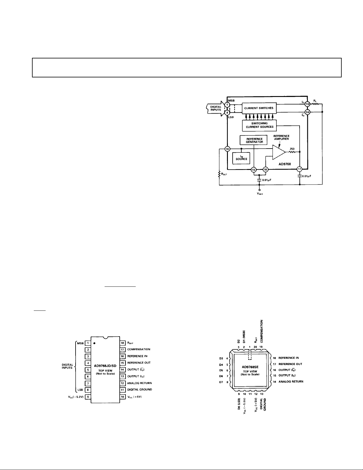
GENERAL DESCRIPTION
The Analog Devices AD9768SD D/A converter is a monolithic
current-output converter which can accept 8 bits of ECL-level
digital input voltages and convert them into analog signals at
update rates as high as 100 MSPS. In addition to its use as a
standard D/A converter, it can also be utilized as a two-quadrant
multiplying D/A at multiplying bandwidths as high as 40 MHz.
An inherently low glitch design is used, and the complementary
current outputs are suitable for driving transmission lines
directly. Nominal full-scale output is 20 mA, which corresponds
to a 1 volt drop across a 50 Ω load, or ±1 volt across 100 Ω
returned to +1 volt. The actual output current is determined by
the on-chip reference voltage (V
current setting resistor, R
Full-scale output current I
calculated with the equation:
The setting resistor R
both have low temperature coefficients. A complementary
is also provided.
I
OUT
SET
OUT
I
=4×
OUT
and the output load resistor should
SET
< –1.26 V) and an external
REF
.
with digital “1” at all inputs is
V
RET–VREF
R
SET
D/A Converter
AD9768
FUNCTIONAL BLOCK DIAGRAM
The reference voltage source is a modified bandgap type
and is nominally –1.26 volts. This reference supply requires
no external regulation. To reduce the possibility of noise
generation and/or instability, Pin 15 (REFERENCE OUT)
can be decoupled using a high-quality ceramic chip
capacitor. Stabilization of the internal loop amplifier is by a
single capacitor connected from Pin 17 (COMPENSATION)
to ground. The minimum value for this capacitor is 3900 pF,
although a 0.01 µF ceramic chip capacitor is recommended.
The incredible speed characteristics of the AD9768SD D/A
converter make it attractive for a wide range of high speed
applications. The ability of the unit to operate as a twoquadrant multiplying D/A converter adds another dimension to its usefulness and makes the AD9768SD a truly
versatile device.
AD9768SE PIN CONNECTIONS
AD9768JD/SD PIN CONNECTIONS
REV. A
Information furnished by Analog Devices is believed to be accurate and
reliable. However, no responsibility is assumed by Analog Devices for its
use, nor for any infringements of patents or other rights of third parties
which may result from its use. No license is granted by implication or
otherwise under any patent or patent rights of Analog Devices.
One Technology Way, P.O. Box 9106, Norwood, MA 02062-9106, U.S.A.
Tel: 617/329-4700 Fax: 617/326-8703
Page 2
(typical @ +258C under following conditions unless otherwise noted; nominal digital
AD9768–SPECIFICA TIONS
Parameter Unit AD9768SJD/SD/SE
RESOLUTION(FS = FULL SCALE) Bits 8
LSB WEIGHT (CURRENT) µA78
ACCURACY
TEMPERATURE COEFFICIENTS
DIGITAL DATA INPUTS
OUTPUT
SPEED PERFORMANCE
REFERENCE
VOLTAGE-MULTIPLYING MODE4 (See Figure 2)
1
Differential Nonlinearity ± % FS 0.2
Integral Nonlinearity ± % FS 0.2
Monotonicity Guaranteed
Zero Offset (lnitial) µA60
Zero Offset ppm/°C 1.5
Reference Voltage (–1.26 V) ppm/°C70
Logic Compatibility ECL
Logic Voltage Levels “l” = V –0.9
“0” = V –1.7
Coding Binary (BIN) = Unipolar Out
Current (Unipolar) FS mA (max) 2 to 20 (30)
I
(@ Pin 13)
OUT
All Digital “1” Input mA 20
All Digital “0” Input mA 0
I
(@ Pin 14)
OUT
All Digital “l” Input mA 0
All Digital “0” Input mA 20
Compliance V (Pin 13) –0.7 to +3.0
Impedance Ω (±15%) 750
Settling Time (to 0.2% FS)
Slew Rate V/µs 400
Update Rate MSPS 100
Rise Time ns 1.8
Glitch Energy pV-sec 200
Internal, Monolithic
External, Variable
Voltage-Multiplying Mode V (max) 0 to –1.1 (–2)
Current-Multiplying Mode mA (max) 0 to –5 (–7.5 )
VM Range (at Pin 16) V ± 0.5
VM Center V –0.6
Resistance (at Pin 16) kΩ 800
Transfer Function – Measured at Pin 13; Digital “0” Applied
2
3
4
Large Signal Bandwidth (–3 dB Point) kHz 250
Offset Binary (OBN) = Bipolar Out
V (Pin 14) –1.1 to +3.0
ns 5
V –1.26
to Bits 1-8:
–0.1 VM Input = 0 mA I
–1.1 VM Input = 0 mA I
Measured at Pin 13; Digital “1” Applied
to Bits 1-8:
–0.1 VM Input = 1 mA I
–1.1 VM Input = 20 mA I
input levels; nominal power supplies; RL = 50 V; R
OUT
OUT
OUT
OUT
= 220 V; V
SET
RET
= 0 V)
Parameter Unit AD9768SJD/SD/SE
CURRENT-MULTIPLYING MODE
(See Figure 4)
IM Range (at Pins 17 & 18) mA 0 to 5
Resistance (at Pin 18) Ω 160
Transfer Function – Measured at Pin 13; Digital “0” Applied
Large Signal Bandwidth (–3dB Point) MHz 40
POWER REQUIREMENTS
–5.2 V ±0.25 mA (max) 66(70)
+5.0 V ±0.25 mA (max) 14(15)
Power Dissipation mW (max) 410(430)
Power Supply Sensitivity
TEMPERATURE RANGES
Operating
AD9768JD °C 0 to +70
AD9768SD/SE °C –55 to +125
Storage °C –55 to +150
THERMAL RESlSTANCE
Junction to Air, θJA (Free Air) °C/W 90
Junction to Case, θ
PACKAGE OPTION
Ceramic (D-18) AD9768JD
5
6
7
JA
8
LCC (E-20A) AD9768SE
NOTES
1
Relative to FS, including linearity (within voltage compliance limits).
2
Worst case settling time; includes FS and Most Significant Bit (MSB) transitions.
3
Applies when operating AD9768 as standard D/A.
4
Based on RL = 50 ohms; R
5
1% change in either power supply voltage causes 0.07% change in analog output.
6
Case temperature.
7
Maximum junction temperature 125°C.
8
D = Ceramic DIP, E = Leadless Ceramic Chip Carrier.
Specifications subject to change without notice.
= 220 ohms; V
SET
to Bits 1-8:
1 mA IM Input = 0 mA I
5 mA IM Input = 0 mA I
Measured at Pin 13; Digital “1” Applied
to Bits 1-8:
1 mA IM Input = 4 mA I
5 mA IM Input = 20 mA I
OUT
OUT
OUT
OUT
%/% 0.07
°C/W 20
AD9768SD
= 0 V.
RET
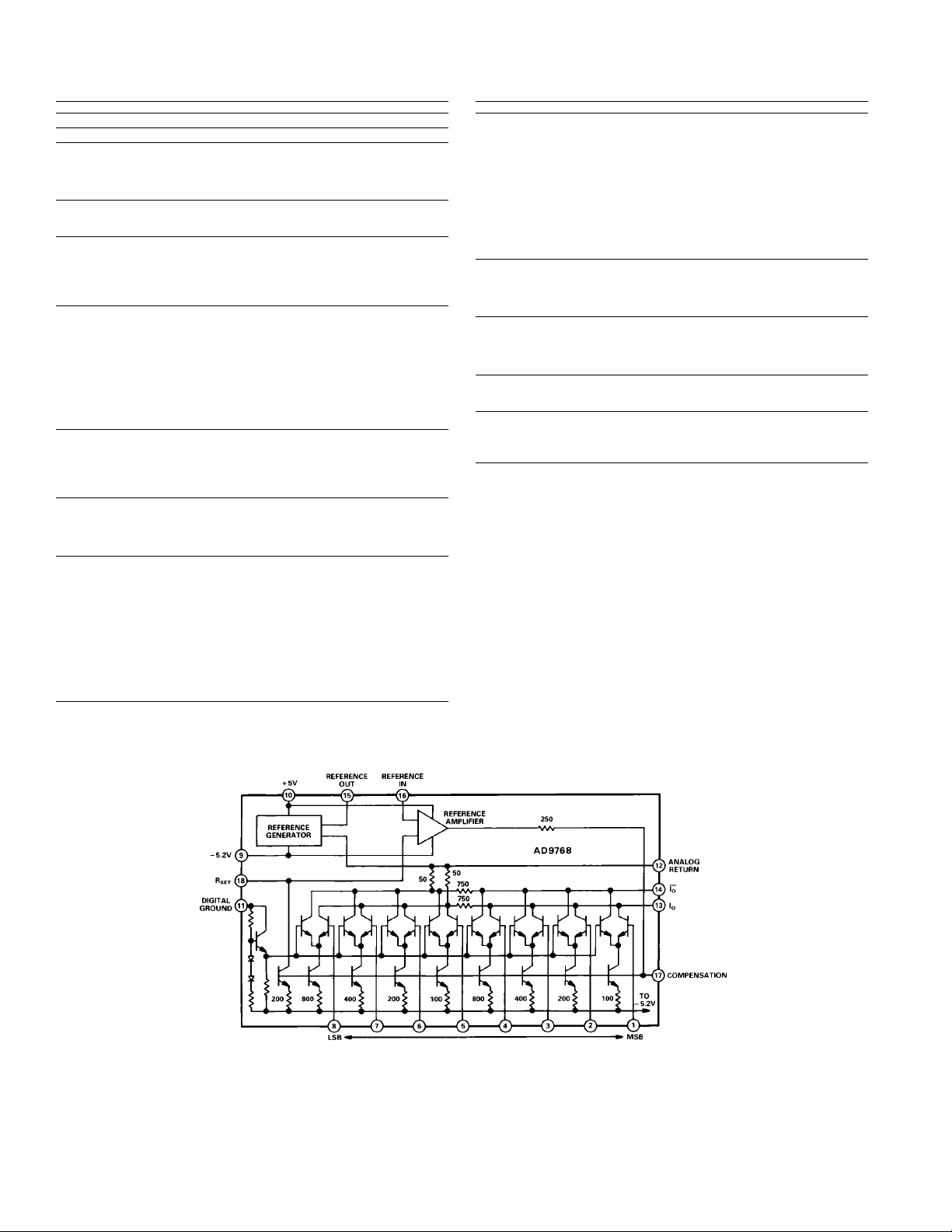
AD9768SD D/A Schematic
–2–
REV. A
Page 3

AD9768
THEORY OF OPERATION
Refer to the AD9768SD schematic.
The transistors pictured on the bottom of the diagram, con-
nected to paired transistors in the middle of the schematic, are
current sources which are always “on”. The paired transistors
are differential current switches, designed to steer current from
the current sources to either Pin 13 (I
) or Pin 14 (
O
).
I
O
Digital inputs applied to Pins 1-8 determine which transistors
will be operating in each pair and establish what current will
flow at Pins 13 and 14.
The transistor on the extreme left of the schematic is a base
reference for the paired current switches and is used to assure
the switches will be centered around an ECL voltage swing. The
diodes connected to the base of this transistor are temperature
compensation devices for the base reference circuit.
There are three different current sources in the AD9768 D/A.
The eight transistors shown on the bottom of the schematic are
structured as two identical groups of four current sources, each
of which is binarily weighted. The MSB group, comprised of the
four on the right, is connected to the LSB group through a 15:1
current divider made up of two 50 Ω and two 750 Ω resistor
networks. The geometry of the AD9768 guarantees the binary
weighing ratios among the 100, 200, 400 and 800 resistors in
each emitter circuit are correct.
The resistor values which are shown indicate the ratios among
the resistors, and not their nominal values.
The third current source is a single transistor, pictured in the
lower left portion of the schematic with its collector connected
to Pin 18 R
. Its function is to help establish the base voltage
SET
on the eight current sources; it works in conjunction with the
external R
resistor selected by the user of the AD9768, and
SET
the reference amplifier. Current flowing through this transistor
is referred to as I
in the figures and text.
M
When the AD9768 is operating as a conventional current-output
D/A converter, I
develops a voltage across R
M
which is one of
SET
the inputs to the on-board reference amplifier shown in the
schematic. The other input to this amplifier is the on-chip
reference voltage of –1.26 volts.
The output of the reference amplifier adjusts the current-source
base reference voltage at Pin 17; this, in turn, adjusts the value
of I
in the single-transistor current source and causes it to
M
develop a voltage across R
which maintains Pin 18 at the
SET
–1.26 volts of the on-chip reference supply.
To maintain good stability in the internal loop reference
amplifier, a ceramic chip capacitor with a nominal value of
0.01 µF should be connected to Pin 17 COMPENSATION;
minimum recommended value for this capacitor is 3900 pF.
The temperature coefficient of the load resistor (R
) can affect
L
the performance of the AD9768 D/A converter, as it can with
any current-output converter. The design and use of the
AD9768 and its dependence on an external R
ever, make it sensitive also to the tempco of R
cautioned to select R
and R
L
resistors which have low tem-
SET
resistor, how-
SET
. The user is
SET
perature coefficients.
DIGITAL GROUND (Pin 11) and ANALOG RETURN (Pin
12) are normally connected together; this connection should be
made as close as possible to the device case to minimize possible
noise problems. The AD9768 D/A is similar to any other high-
REV. A
–3–
speed, high performance device: optimum use requires careful
attention to all design details, including the layout of the circuit
in which the converter is used.
CONVENTIONAL AD9768SD
Refer to Figure 1, Conventional AD9768SD.
The output current of the AD9768 appears at Pin 13 (I
develops a voltage across the load resistor R
(the current flowing through the single-transistor
A. I
M
which is based on:
L
) and
O
source discussed above)
B. Value of R
L
Figure 1. Conventional AD9768SD
IM is a function of the return voltage (V
voltage (V
), and the value of R
REF
SET
), the reference
RET
; all of these are selected by
the user for his application. The necessary equations for
calculating precise values for each are part of Figure 1. As
indicated, the voltage drop across R
voltage; the resulting voltage is the total V
is added to the return
L
of the converter.
OUT
VOLTAGE MULTIPLYING MODE
In addition to its use as an ultra-high speed current output D/A
converter, the AD9768 can also be used as a two-quadrant
multiplying D/A in either a voltage mode or a current mode.
Refer to Figure 2, Multiplying AD9768 (Voltage Mode).
When operating in this mode, the analog output of the AD9768
is influenced by the digital inputs and an external multiplying
voltage (V
) applied to Pin 16 REFERENCE IN, which takes
M
the place of the internal reference used when the D/A is
operating in a conventional manner.
Figure 2. Multiplying AD9768 (Voltage Mode)
The value of IM flowing through R
V
minus the multiplying voltage (VM), divided by R
RET
is set by the voltage of
SET
SET
; the
amount of this current is part of the equation which establishes
the analog output (V
) of the AD9768 and is chosen by the
OUT
user for his application. As it is when operating the D/A in a
conventional fashion, V
+3 volts. V
(for purposes of discussion here) is some negative
M
can be any value between 0 volts and
RET
voltage and can be varied over a range which is approximately 1
volt peak-to-peak.
Page 4

AD9768
If the load resistor (RL) has a value of 50 ohms, if R
value of 220 ohms, and if V
is 0 V, the center of the V
RET
voltage will be –0.6 V; and it can vary from –0.1 V to –1.1 V.
Typically, the frequency of these variations has an upper limit of
250 kHz when operating in the voltage multiplying mode; that
frequency is the 3 dB point of the bandwidth of the internal
reference amplifier.
The combined effects of variations in V
input values are shown in Figure 3, I
and changes in digital
M
vs. Multiplying Volt-
OUT
age. In this illustration, the ordinate of the graph is expressed in
terms of milliamps of I
will be a function of the value of R
current at Pin 13. V
OUT
chosen by the user.
L
OUT
has a
SET
M
, of course,
is some voltage chosen by the user for his particular applica-
V
IN
tion; the value of this voltage is based in part on the size of the
load resistor and the 0 mA to 5 mA range of I
frequency components as high as 40 MHz. V
. VIN can have
M
and R
ADJ
ADJ
provide an offset adjustment to compensate for the dc component
of V
to assure IM is always a unipolar current between 0 mA
IN
and 5 mA. The values of the required voltages and resistors can
be calculated using the equations which are part of Figure 4.
Refer to Figure 5, I
vs. Multiplying Current.
OUT
C753c–5–12/89
Figure 3. I
vs. Multiplying Voltage
OUT
The negative value of VM on the horizontal axis is shown starting at approximately –0.1 V, rather than 0 V, because the
AD9768 must have some small value of voltage applied to perform a multiplying function. For the conditions shown in the
figure, output current starts to become nonlinear at approximately 20 mA because of the maximum 30 mA output drive
capabilities of the device. Different values for R
SET
and R
L
would alter the point where limiting first appears.
CURRENT MULTIPLYING MODE
The AD9768 D/A converter can be operated at markedly higher
multiplying rates when operated in a current-multiplying mode,
as contrasted with the voltage multiplying mode. Refer to Figure
4, Multiplying AD9768SD (Current Mode).
Figure 5. I
vs. Multiplying Current
OUT
As shown, IM can vary over the range of 0 mA to 5 mA; a value
of approximately 0.3 mA may be the practical lower limit because
of nonlinearities at extremely small current levels. These changes
in I
are combined with variations in digital inputs, producing
M
complex changes in the output current (at pin 13) and in V
OUT
.
The “rounding” of the current curve in the graph is the result of
I
approaching the 30 mA maximum drive capabilities of the
OUT
AD9768 and needs to be taken into account to assure optimum
performance in the selected application.
OUTLINE DIMENSIONS
Dimensions shown in inches and (mm).
Ceramic (D-18)
Figure 4. Multiplying AD9768SD (Current Mode)
In this mode, the internal reference amplifier and its inherent
frequency limitations are replaced by a current source comprised
of U1 and associated circuits. These circuits supply a unipolar
current I
which is one-fourth the full-scale output current
M
(with digital “1” applied to all inputs) and set current flow
through the load resistor.
–4–
LCC (E-20A)
PRINTED IN U.S.A.
REV. A
 Loading...