

Page 1
a
14-Bit, 300 MSPS
High Speed TxDAC+
®
D/A Converter
FEATURES
14-Bit Dual Muxed Port DAC
300 MSPS Output Update Rate
Excellent SFDR and IMD Performance
SFDR to Nyquist @ 25 MHz Output: 71 dB
Internal Clock Doubling PLL
Differential or Single-Ended Clock Input
On-Chip 1.2 V Reference
Single 3.3 V Supply Operation
Power Dissipation: 155 mW @ 3.3 V
48-Lead LQFP
APPLICATIONS
Communications: LMDS, LMCS, MMDS
Base Stations
Digital Synthesis
QAM and OFDM
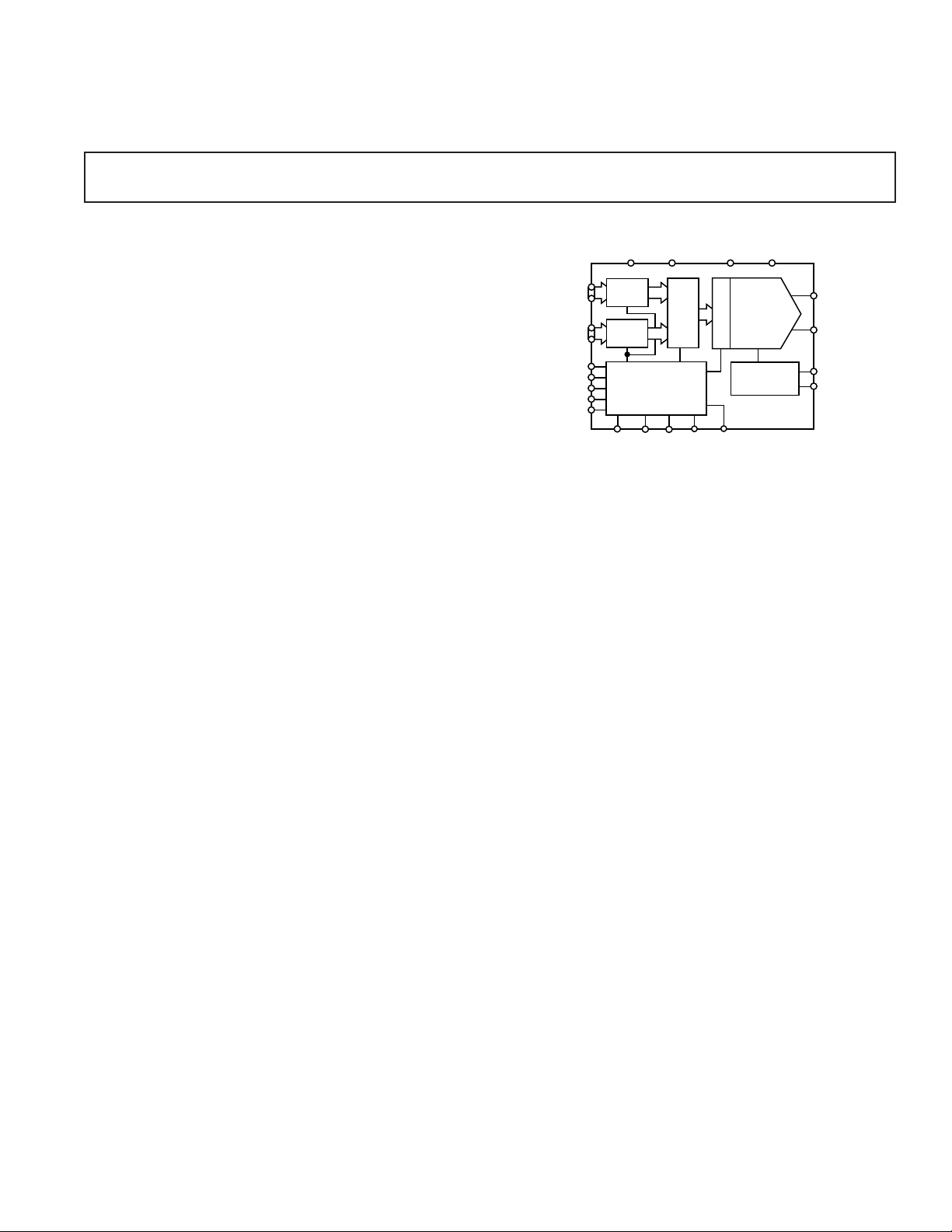
PRODUCT DESCRIPTION
The AD9755 is a dual, muxed port, ultrahigh speed, singlechannel, 14-bit CMOS DAC. It integrates a high quality 14-bit
TxDAC+
core, a voltage reference, and digital interface circuitry
into a small 48-lead LQFP package. The AD9755 offers exceptional ac and dc performance while supporting update rates up
to 300 MSPS.
The AD9755 has been optimized for ultrahigh speed applications up to 300 MSPS where data rates exceed those possible on
a single data interface port DAC. The digital interface consists
of two buffered latches as well as control logic. These latches
can be time multiplexed to the high speed DAC in several ways.
This PLL drives the DAC latch at twice the speed of the externally applied clock and is able to interleave the data from the
two input channels. The resulting output data rate is twice that
of the two input channels. With the PLL disabled, an external
2× clock may be supplied and divided by two internally.
The CLK inputs (CLK+/CLK–) can be driven either differentially
or single-ended, with a signal swing as low as 1 V p-p.
AD9755
*
FUNCTIONAL BLOCK DIAGRAM
DVDD
DCOM
PORT1
PORT2
CLK+
CLK–
CLKVDD
PLLVDD
CLKCOM
LATCH
LATCH
PLL
CLOCK
MULTIPLIER
RESET LPF DIV0 DIV1 PLLLOCK
The DAC utilizes a segmented current source architecture combined with a proprietary switching technique to reduce glitch
energy and maximize dynamic accuracy. Differential current
outputs support single-ended or differential applications. The
differential outputs each provide a nominal full-scale current
from 2 mA to 20 mA.
The AD9755 is manufactured on an advanced low cost 0.35 µm
CMOS process. It operates from a single supply of 3.0 V to 3.6 V
and consumes 155 mW of power.
PRODUCT HIGHLIGHTS
1. The AD9755 is a member of a pin compatible family of high
speed TxDAC+s providing 10-, 12-, and 14-bit resolution.
2. Ultrahigh Speed 300 MSPS Conversion Rate.
3. Dual 14-Bit Latched, Multiplexed Input Ports. The AD9755
features a flexible digital interface allowing high speed data
conversion through either a single or dual port input.
4. Low Power. Complete CMOS DAC function operates on
155 mW from a 3.0 V to 3.6 V single supply. The DAC fullscale current can be reduced for lower power operation.
5. On-Chip Voltage Reference. The AD9755 includes a 1.20 V
temperature compensated band gap voltage reference.
MUX
AVDD ACOM
DAC
DAC LATCH
REFERENCE
AD9755
I
OUTA
I
OUTB
REFIO
FSADJ
*Protected by U.S. Patent numbers 5450084, 5568145, 5689257, and 5703519.
Other patents pending.
REV. B
Information furnished by Analog Devices is believed to be accurate and
reliable. However, no responsibility is assumed by Analog Devices for its
use, nor for any infringements of patents or other rights of third parties that
may result from its use. No license is granted by implication or otherwise
under any patent or patent rights of Analog Devices. Trademarks and
registered trademarks are the property of their respective companies.
One Technology Way, P.O. Box 9106, Norwood, MA 02062-9106, U.S.A.
Tel: 781/329-4700 www.analog.com
Fax: 781/326-8703 © 2003 Analog Devices, Inc. All rights reserved.
Page 2

AD9755
DC SPECIFICATIONS
–SPECIFICATIONS
(T
to T
MIN
otherwise noted.)
, AVDD = 3.3 V, DVDD = 3.3 V, PLLVDD = 3.3 V, CLKVDD = 3.3 V, I
MAX
= 20 mA, unless
OUTFS
Parameter Min Typ Max Unit
RESOLUTION 14 Bits
DC ACCURACY
1
Integral Linearity Error (INL) –5 ±2.5 +5 LSB
Differential Nonlinearity (DNL) –3 ±1.5 +3 LSB
ANALOG OUTPUT
Offset Error –0.025 ±0.01 +0.025 % of FSR
Gain Error (Without Internal Reference) –2 ±0.5 +2 % of FSR
Gain Error (With Internal Reference) –2 ±0.25 +2 % of FSR
Full-Scale Output Current
2
2.0 20.0 mA
Output Compliance Range –1.0 +1.25 V
Output Resistance 100 kΩ
Output Capacitance 5 pF
REFERENCE OUTPUT
Reference Voltage 1.14 1.20 1.26 V
Reference Output Current
3
100 nA
REFERENCE INPUT
Input Compliance Range 0.1 1.25 V
Reference Input Resistance 1 MΩ
TEMPERATURE COEFFICIENTS
Offset Drift 0 ppm of FSR/°C
Gain Drift (Without Internal Reference) ±50 ppm of FSR/°C
Gain Drift (With Internal Reference) ±100 ppm of FSR/°C
Reference Voltage Drift ±50 ppm/°C
POWER SUPPLY
Supply Voltages
AVDD 3.0 3.3 3.6 V
DVDD 3.0 3.3 3.6 V
PLLVDD 3.0 3.3 3.6 V
CLKVDD 3.0 3.3 3.6 V
Analog Supply Current (I
Digital Supply Current (I
PLL Supply Current (I
Clock Supply Current (I
Power Dissipation
Power Dissipation
4
(3 V, I
5
(3 V, I
PLLVDD
Power Supply Rejection Ratio
4
)
AVDD
4
)
DVDD
4
)
4
)
CLKVDD
= 20 mA) 155 165 mW
OUTFS
= 20 mA) 216 mW
OUTFS
6
—AVDD –1 +1 % of FSR/V
33 36 mA
3.5 4.5 mA
4.5 5.1 mA
10.0 11.5 mA
Power Supply Rejection Ratio6—DVDD –0.04 +0.04 % of FSR/V
OPERATING RANGE –40 +85 °C
NOTES
1
Measured at I
2
Nominal full-scale current, I
3
An external buffer amplifier is recommended to drive any external load.
4
100 MSPS f
5
300 MSPS f
6
±5% power supply variation.
Specifications subject to change without notice.
, driving a virtual ground.
OUTA
with PLL on, f
DAC
.
DAC
OUTFS
, is 32× the I
= 100 MHz, all supplies = 3.0 V.
OUT
current.
REF
–2–
REV. B
Page 3

AD9755
(T
to T
, AVDD = 3.3 V, DVDD = 3.3 V, PLLVDD = 0 V, CLKVDD = 3.3 V, I
MAX
DYNAMIC SPECIFICATIONS
MIN
Differential Transformer-Coupled Output, 50 ⍀ Doubly Terminated, unless otherwise noted.)
Parameter Min Typ Max Unit
DYNAMIC PERFORMANCE
Maximum Output Update Rate (f
Output Settling Time (t
Output Propagation Delay (t
Glitch Impulse
1
) (to 0.1%)
ST
PD
Output Rise Time (10% to 90%)
Output Fall Time (90% to 10%)
Output Noise (I
Output Noise (I
= 20 mA) 50 pA/√Hz
OUTFS
= 2 mA) 30 pA/√Hz
OUTFS
) 300 MSPS
DAC
1
1
)
1
1
11 ns
1ns
5 pV-s
2.5 ns
2.5 ns
AC LINEARITY
Spurious-Free Dynamic Range to Nyquist
= 100 MSPS; f
f
DAC
= 1.00 MHz
OUT
0 dBFS Output 74 84 dBc
–6 dBFS Output 77 dBc
–12 dBFS Output 79 dBc
= 65 MSPS; f
f
DATA
= 65 MSPS; f
f
DATA
f
= 65 MSPS; f
DATA
= 65 MSPS; f
f
DATA
= 65 MSPS; f
f
DATA
f
= 160 MSPS; f
DAC
= 160 MSPS; f
f
DAC
= 160 MSPS; f
f
DAC
f
= 160 MSPS; f
DAC
= 160 MSPS; f
f
DAC
= 300 MSPS; f
f
DAC
f
= 300 MSPS; f
DAC
= 300 MSPS; f
f
DAC
= 300 MSPS; f
f
DAC
f
= 300 MSPS; f
DAC
= 1.1 MHz
OUT
= 5.1 MHz
OUT
= 10.1 MHz
OUT
= 20.1 MHz
OUT
= 30.1 MHz
OUT
= 1.1 MHz 80 dBc
OUT
= 11.1 MHz 77 dBc
OUT
= 31.1 MHz 72 dBc
OUT
= 51.1 MHz 72 dBc
OUT
= 71.1 MHz 69 dBc
OUT
= 1.1 MHz 80 dBc
OUT
= 26.1 MHz 71 dBc
OUT
= 51.1 MHz 67 dBc
OUT
= 101.1 MHz 61 dBc
OUT
= 141.1 MHz 60 dBc
OUT
2
2
2
2
2
79 dBc
79 dBc
78 dBc
74 dBc
70 dBc
Spurious-Free Dynamic Range within a Window
= 100 MSPS; f
f
DAC
= 1 MHz; 2 MHz Span
OUT
0 dBFS Output 83.5 93 dBc
= 65 MSPS; f
f
DAC
= 150 MSPS; f
f
DAC
= 5.02 MHz; 2 MHz Span 85 dBc
OUT
= 5.04 MHz; 4 MHz Span 85 dBc
OUT
Total Harmonic Distortion
= 100 MSPS; f
f
DAC
= 25°C –83 –73 dBc
T
A
T
to T
MIN
= 65 MHz; f
f
DAC
= 160 MHz; f
f
DAC
MAX
= 1.00 MHz
OUT
–83 –71 dBc
= 2.00 MHz –78 dBc
OUT
= 2.00 MHz –78 dBc
OUT
Multitone Power Ratio (Eight Tones at 110 kHz Spacing)
= 65 MSPS; f
f
DAC
= 2.00 MHz to 2.77 MHz
OUT
0 dBFS Output 75 dBc
–6 dBFS Output 73 dBc
–12 dBFS Output 70 dBc
NOTES
1
Measured single-ended into 50 Ω load.
2
Single Port Mode (PLL disabled, DIV0 = 1, DIV1 = 0, data on Port 1).
Specifications subject to change without notice.
OUTFS
= 20 mA,
REV. B
–3–
Page 4

AD9755
DIGITAL SPECIFICATIONS
(T
to T
MIN
, AVDD = DVDD = PLLVDD = CLKVDD = 3.3 V, I
MAX
= 20 mA, unless otherwise noted.)
OUTFS
Parameter Min Typ Max Unit
DIGITAL INPUTS
Logic 1 2.1 3 V
Logic 0 0 0.9 V
Logic 1 Current –10 +10 µA
Logic 0 Current –10 +10 µA
Input Capacitance 5 pF
Input Setup Time (t
Input Hold Time (t
Latch Pulsewidth (t
Input Setup Time (t
Input Hold Time (t
), TA = 25°C 1.0 0.5 ns
S
), TA = 25°C 1.0 0.5 ns
H
), TA = 25°C 1.5 ns
LPW
PLLVDD = 0 V), TA = 25°C –1.0 –1.5 ns
S,
PLLVDD = 0 V), TA = 25°C 2.5 1.7 ns
H,
CLK to PLLLOCK Delay (tD, PLLVDD = 0 V), TA = 25°C 3.5 4.0 ns
Latch Pulsewidth (t
PLLOCK (V
OH
PLLVDD = 0 V), TA = 25°C 1.5 ns
LPW
) 3.0 V
PLLOCK (VOL) 0.3 V
CLK INPUTS
Input Voltage Range 0 3 V
Common-Mode Voltage 0.75 1.5 2.25 V
Differential Voltage 0.5 1.5 V
Min CLK Frequency* 6.25 MHz
*Min CLK Frequency only applies when using internal PLL. When PLL is disabled, there is no minimum CLK frequency.
Specifications subject to change without notice.
–4–
REV. B
Page 5
AD9755
ABSOLUTE MAXIMUM RATINGS*
Parameter With Respect To Min Max Unit
AVDD, DVDD, CLKVDD, PLLVDD ACOM, DCOM, CLKCOM, PLLCOM –0.3 +3.9 V
AVDD, DVDD, CLKVDD, PLLVDD AVDD, DVDD, CLKVDD, PLLVDD –3.9 +3.9 V
ACOM, DCOM, CLKCOM, PLLCOM ACOM, DCOM, CLKCOM, PLLCOM –0.3 +0.3 V
REFIO, REFLO, FSADJ ACOM –0.3 AVDD + 0.3 V
, I
I
OUTA
OUTB
Digital Data Inputs (DB13 to DB0) DCOM –0.3 DVDD + 0.3 V
CLK+/CLK–, PLLLOCK CLKCOM –0.3 CLKVDD + 0.3 V
DIV0, DIV1, RESET CLKCOM –0.3 CLKVDD + 0.3 V
LPF PLLCOM –0.3 PLLVDD + 0.3 V
Junction Temperature 150 °C
Storage Temperature –65 +150 °C
Lead Temperature (10 sec) 300 °C
*Stresses above those listed under Absolute Maximum Ratings may cause permanent damage to the device. This is a stress rating only; functional operation of the device
at these or any other conditions above those indicated in the operational sections of this specification is not implied. Exposure to absolute maximum ratings for extended
periods may affect device reliability.
t
t
H
S
ACOM –1.0 AVDD + 0.3 V
PORT 1
DATA IN
PORT 2
DATA X
ORDERING GUIDE
DATA Y
Temperature Package Package
INPUT CLK
(PLL ENABLED)
OR I
I
OUTA
OUTB
t
LPW
t
PD
DATA X
t
PD
DATA Y
Model Range Description Option
AD9755AST –40°C to +85°C48-Lead LQFP ST-48
AD9755ASTRL –40°C to +85°C48-Lead LQFP ST-48
AD9755-EB Evaluation
THERMAL CHARACTERISTIC
Figure 1. I/O Timing
Thermal Resistance
48-Lead LQFP
= 91°C/W
θ
JA
CAUTION
ESD (electrostatic discharge) sensitive device. Electrostatic charges as high as 4000 V readily
accumulate on the human body and test equipment and can discharge without detection. Although
the AD9755 features proprietary ESD protection circuitry, permanent damage may occur on
devices subjected to high energy electrostatic discharges. Therefore, proper ESD precautions are
recommended to avoid performance degradation or loss of functionality.
Board
REV. B
–5–
Page 6
AD9755
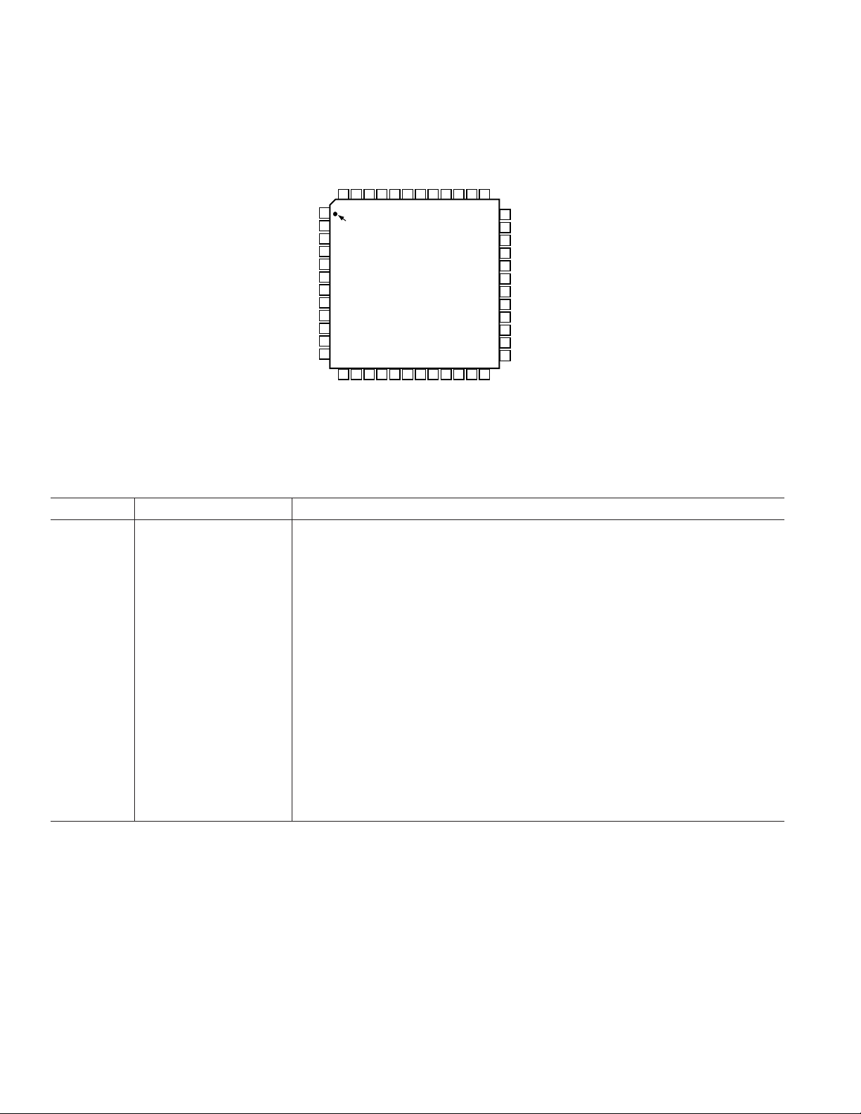
PIN CONFIGURATION
LPF
CLKCOM
ACOM
AD9755
TOP VIEW
(Not to Scale)
P1B5
P1B4
P1B3
OUTAIOUTB
I
P1B2
P1B1
AVDD
FSADJ
REFIO
DVDD
DCOM
LSB–P1B0
DIV1
DIV0
36
35
34
33
32
31
30
29
28
27
26
25
P2B12
MSB–P2B13
P2B0–LSB
P2B1
P2B2
P2B3
P2B4
P2B5
P2B6
P2B7
P2B8
P2B9
P2B10
P2B11
RESET
CLK+
CLK–
DCOM
DVDD
PLLLOCK
MSB–P1B13
P1B12
P1B11
P1B10
P1B9
P1B8
CLKVDD
PLLVDD
48 47 46 45 44 39 38 3743 42 41 40
1
PIN 1
2
IDENTIFIER
3
4
5
6
7
8
9
10
11
12
13 14 15 16 17 18 19 20 21 22 23 24
P1B7
P1B6
PIN FUNCTION DESCRIPTIONS
Pin No. Mnemonic Description
1 RESET Internal Clock Divider Reset
2 CLK+ Differential Clock Input
3 CLK– Differential Clock Input
4, 22 DCOM Digital Common
5, 21 DVDD Digital Supply Voltage
6PLLLOCK Phase-Locked Loop Lock Indicator Output
7–20 P1B13–P1B0 Data Bits P1B13 to P1B0, Port 1
23–36 P2B13–P2B0 Data Bits P2B13 to P2B0, Port 2
37, 38 DIV0, DIV1 Control Inputs for PLL and Input Port Selector Mode; see Tables I and II for details.
39 REFIO Reference Input/Output
40 FSADJ Full-Scale Current Output Adjust
41 AVDD Analog Supply Voltage
42 I
43 I
OUTB
OUTA
Differential DAC Current Output
Differential DAC Current Output
44 ACOM Analog Common
45 CLKCOM Clock and Phase-Locked Loop Common
46 LPF Phase-Locked Loop Filter
47 PLLVDD Phase-Locked Loop Supply Voltage
48 CLKVDD Clock Supply Voltage
–6–
REV. B
Page 7
AD9755
TERMINOLOGY
Linearity Error (Also Called Integral Nonlinearity or INL)
Linearity error is defined as the maximum deviation of the actual
analog output from the ideal output, determined by a straight
line drawn from zero to full scale.
Differential Nonlinearity (DNL)
DNL is the measure of the variation in analog value, normalized
to full scale, associated with a 1 LSB change in digital input code.
Monotonicity
A D/A converter is monotonic if the output either increases or
remains constant as the digital input increases.
Offset Error
The deviation of the output current from the ideal of zero is
called offset error. For I
inputs are all 0s. For I
, 0 mA output is expected when the
OUTA
, 0 mA output is expected when the
OUTB
inputs are all 1s.
Gain Error
The difference between the actual and ideal output span. The
actual span is determined by the output when all inputs are set
to 1s, minus the output when all inputs are set to 0s.
Output Compliance Range
The range of allowable voltage at the output of a current-output
DAC. Operation beyond the maximum compliance limits may
cause either output stage saturation or breakdown, resulting in
nonlinear performance.
Temperature Drift
Specified as the maximum change from the ambient (25°C) value
to the value at either T
MIN
or T
. For offset and gain drift, the
MAX
drift is reported in ppm of full-scale range (FSR) per degree C.
For reference drift, the drift is reported in ppm per degree C.
Power Supply Rejection
The maximum change in the full-scale output as the supplies
are varied from minimum to maximum specified voltages.
Settling Time
The time required for the output to reach and remain within a
specified error band around its final value, measured from the
start of the output transition.
Glitch Impulse
Asymmetrical switching times in a DAC cause undesired output
transients that are quantified by a glitch impulse. It is specified
as the net area of the glitch in pV-s.
Spurious-Free Dynamic Range
The difference, in dB, between the rms amplitude of the output
signal and the peak spurious signal over the specified bandwidth.
Total Harmonic Distortion (THD)
THD is the ratio of the rms sum of the first six harmonic components to the rms value of the measured fundamental. It is
expressed as a percentage or in decibels (dB).
Signal-to-Noise Ratio (SNR)
SNR is the ratio of the rms value of the measured output signal
to the rms sum of all other spectral components below the
Nyquist frequency, excluding the first six harmonics and dc.
The value for SNR is expressed in decibels.
Adjacent Channel Power Ratio (ACPR)
A ratio in dBc between the measured power within a channel
relative to its adjacent channel.
0.1F
R
2k⍀
SET
1.2V REF
REFIO
FSADJ
DCOM
AD9755
ACOM
3.0V TO 3.6V
DVDD
AVDD
PMOS CURRENT
SOURCE ARRAY
PORT 1 LATCH
DB0 – DB13
SEGMENTED
SWITCHES FOR
DB0 TO DB13
DAC LATCH
2–1 MUX
PORT 2 LATCH
DIGITAL DATA INPUTS
TEKTRONIX DG2020
AWG2021 w/OPTION 4
LECROY 9210
PULSE GENERATOR
(FOR DATA RETIMING)
DB0 – DB13
OR
DAC
CIRCUITS
CIRCUITRY
CLK+
CLK–
MINI
T1-1T
PLL ENABLED
PLL DISABLED
Figure 2. Basic AC Characterization Test Setup
PLL
I
OUTA
I
OUTB
PLLVDD
CLKVDD
RESET
LPF
CLKCOM
DIV0
DIV1
PLLLOCK
1k⍀
1k⍀
HP8644
SIGNAL
GENERATOR
50⍀
50⍀
3.0V TO 3.6V
MINI
CIRCUITS
T1-1T
TO ROHDE &
SCHWARZ
FSEA30
SPECTRUM
ANALYZER
REV. B
–7–
Page 8
AD9755–Typical Performance Characteristics
f
OUT
(MHz)
90
70
40
1000
SFDR (dBc)
80
60
50
20 40 60 80 120 140 160
0dBmFS
–6dBmFS
–12dBmFS
f
OUT
(MHz)
90
70
40
1000
SFDR (dBc)
80
60
50
20 40 60 80 120 140 160
SFDR CLOSE TO CARRIERS
(2F1-F2, 2F2-F1)
SFDR OVER NYQUIST BAND
A
OUT
(dBm)
90
70
40
–6–16
SFDR (dBc)
80
60
50
–14 –12 –10 –8 –4 –2 0–18–20
18.18/19.18MHz
@ 200MSPS
11.82/12.82MHz
@ 130MSPS
27.27/28.27MHz
@ 300MSPS
90
80
–6dBmFS
70
60
SFDR (dBc)
50
40
0dBmFS
–12dBmFS
10 15 20 25 30
f
(MHz)
OUT
TPC 1. Single-Tone SFDR vs. f
= 65 MSPS; Single Port Mode
f
DAC
90
65MSPS
80
70
60
SFDR (dBc)
200MSPS
OUT
3550
@
90
80
70
–6dBmFS
60
SFDR (dBc)
50
40
0dBmFS
–12dBmFS
20 30 40 50 60 70 80 90
f
(MHz)
OUT
TPC 2. Single-Tone SFDR vs. f
= 200 MSPS
f
DAC
90
80
70
60
SFDR (dBc)
SFDR NEAR CARRIERS
(2F1-F2, 2F2-F1)
SFDR OVER
NYQUIST BAND
OUT
100100
@
TPC 3. Single-Tone SFDR vs. f
= 300 MSPS
f
DAC
OUT
@
50
40
TPC 4. SFDR vs. f
90
80
70
60
SFDR (dBc)
50
40
TPC 7. Single-Tone SFDR vs. A
@ f
300MSPS
20 40 60 80 120 140
11.82MHz @ 130MSPS
–14 –12 –10 –8 –4 –2 0
= f
OUT
f
OUT
18.18MHz @ 200MSPS
27.27MHz @ 300MSPS
A
OUT
/11
DAC
(MHz)
OUT
–6–16
(dB)
1000
@ 0 dBFS
OUT
50
40
TPC 5. Two-Tone IMD vs. f
f
DAC
20 30 40 50 60 70 80 90
f
(MHz)
OUT
OUT
= 200 MSPS, 1 MHz Spacing
between Tones, 0 dBFS
90
80
70
60
SFDR (dBc)
50
40
–14 –12 –10 –8 –4 –2 0
26MHz @ 130MSPS
40MHz @ 200MSPS
60MHz @ 300MSPS
–6–16
A
(dBm)
OUT
TPC 8. Single-Tone SFDR vs. A
@ f
= f
DAC
/5
OUT
@
OUT
100100
TPC 6. Two-Tone IMD vs. f
f
= 300 MSPS, 1 MHz Spacing
DAC
OUT
@
between Tones, 0 dBFS
TPC 9. Two-Tone IMD (Third Order
Products) vs. A
OUT
@ f
OUT
= f
DAC
/11
–8–
REV. B
Page 9
AD9755
)
90
11.82MHz/12.82MHz
80
70
60
SFDR (dBc)
50
40
@ 130MSPS
18.18MHz/19.18MHz
@ 200MSPS
27.27MHz/28.27MHz
@ 300MSPS
–14 –12 –10 –8 –4 –2 0–18–20
A
(dBm)
OUT
–6–16
TPC 10. Two-Tone IMD (to Nyquist)
vs. A
@ f
OUT
90
85
80
75
70
65
SINAD (dBm)
60
55
50
= f
OUT
DAC
100 150 200 250
f
(MHz)
DAC
TPC 13. SINAD vs. f
/11
DAC
@ f
OUT
30050
=
10 MHz, 0 dBFS
90
80
70
60
SFDR (dBc)
50
40
26MHz/27MHz
@ 130MSPS
–14 –12 –10 –8 –4 –2 0–18–20
A
OUT
(dBm)
40MHz/41MHz
@ 200MSPS
60MHz/61MHz
@ 300MSPS
–6–16
TPC 11. Two-Tone IMD (Third Order
Products) vs. A
75
70
65
60
55
SFDR (dBc)
50
45
40
I
OUTFS
I
= 5mA
OUTFS
40 60 80 100 120
TPC 14. SFDR vs. I
OUT
I
OUTFS
f
OUT
@ f
= 20mA
= 10mA
(MHz)
OUTFS
OUT
= f
, f
DAC
140
DAC
/5
160200
=
300 MSPS @ 0 dBFS
90
60MHz/61MHz
@ 300MSPS
–14 –12 –10 –8 –4 –2 0–18–20
A
OUT
26MHz/27MHz
@ 130MSPS
40MHz/41MHz
@ 200MSPS
–6–16
(dBm)
80
70
60
SFDR (dBc)
50
40
TPC 12. Two-Tone IMD (to Nyquist)
vs. A
80
75
70
65
60
SFDR (dBc)
55
50
45
40
OUT
@ f
= f
DAC
10MHz
40MHz
80MHz
120MHz
/5
OUT
–10 10 30 50
TEMPERATURE (ⴗC
90–30–50
70
TPC 15. SFDR vs. Temperature,
f
= 300 MSPS @ 0 dBFS
DAC
2.0
1.5
1.0
0.5
0
INL (LSB)
–0.5
–1.0
–1.5
–2.0
0
REV. B
2048
6144
4096 8192
CODE
10240 14336
TPC 16. Typical INL
12288
16383
2
1
DNL (LSB)
0
–1
6144
20480
4096
TPC 17. Typical DNL
10240 14336
8192
CODE
–9–
12288 16383
0
–10
–20
–30
–40
–50
–60
AMPLITUDE (dBm)
–70
–80
–90
–100
f
= 300MSPS
DAC
f
= 24MHz
OUT1
f
= 25MHz
OUT2
f
= 26MHz
OUT3
= 27MHz
f
OUT4
f
= 28MHz
OUT5
f
= 29MHz
OUT6
f
= 30MHz
OUT7
f
= 31MHz
OUT8
SFDR = 58dBc
MAGNITUDE = 0dBFS
40 60 100 120
200
80
FREQUENCY (MHz)
TPC 18. Eight-Tone SFDR @ f
f
DAC
/11, f
= 300 MSPS
DAC
OUT
140
≈
Page 10

AD9755
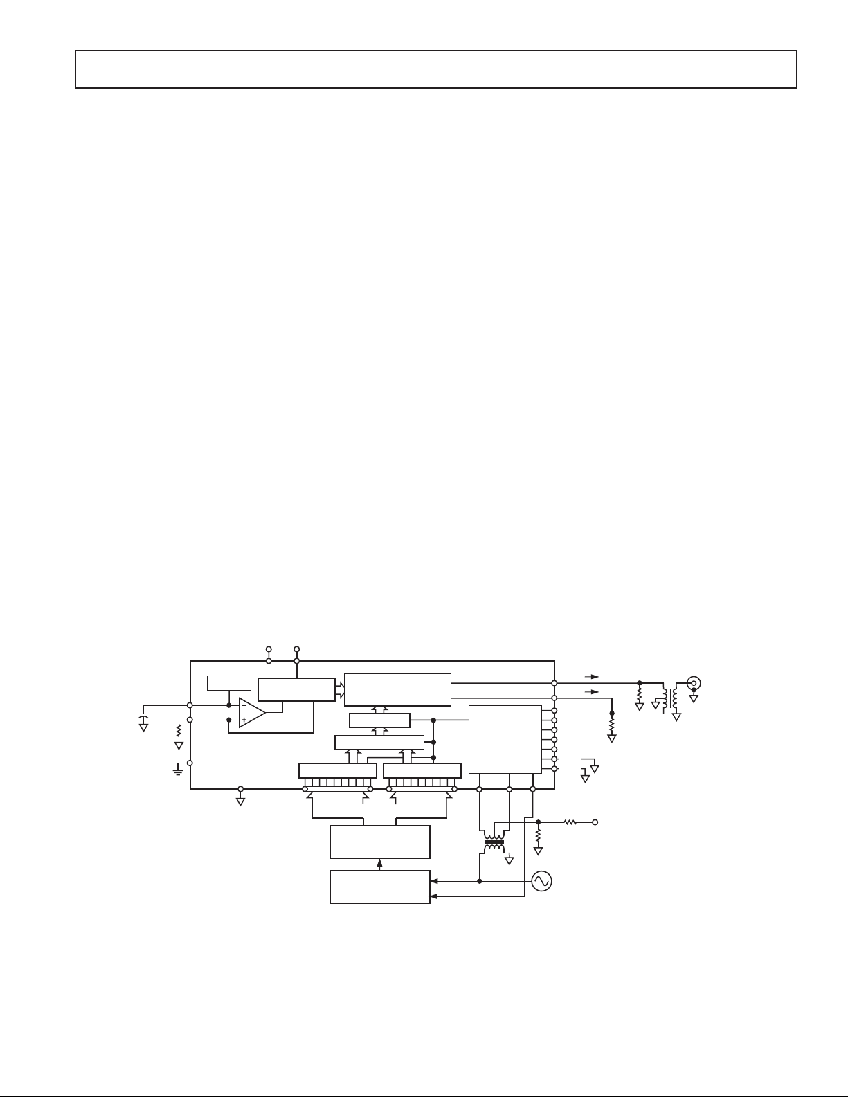
FUNCTIONAL DESCRIPTION
Figure 3 shows a simplified block diagram of the AD9755. The
AD9755 consists of a PMOS current source array capable of
providing up to 20 mA of full-scale current, I
. The array is
OUTFS
divided into 31 equal sources that make up the five most significant
bits (MSBs). The next four bits, or middle bits, consist of 15 equal
current sources whose value is 1/16th of an MSB current source.
The remaining LSBs are a binary weighted fraction of the middle
bit current sources. Implementing the middle and lower bits
with current sources, instead of an R-2R ladder, enhances dynamic
performance for multitone or low amplitude signals and helps
maintain the DAC’s high output impedance (i.e., >100 kΩ).
All of the current sources are switched to one or the other of the
two outputs (i.e., I
OUTA
or I
) via PMOS differential current
OUTB
switches. The switches are based on a new architecture that
significantly improves distortion performance. This new switch
architecture reduces various timing errors and provides matching
complementary drive signals to the inputs of the differential
current switches.
The analog and digital sections of the AD9755 have separate
power supply inputs (i.e., AVDD and DVDD) that can operate
independently over a 3.0 V to 3.6 V range. The digital section,
which is capable of operating at a 300 MSPS clock rate, consists
of edge-triggered latches and segment decoding logic circuitry.
The analog section includes the PMOS current sources, the
associated differential switches, a 1.20 V band gap voltage
reference, and a reference control amplifier.
The full-scale output current is regulated by the reference
control amplifier and can be set from 2 mA to 20 mA via an
external resistor, R
. The external resistor, in combination
SET
with both the reference control amplifier and voltage reference
, sets the reference current I
V
REFIO
, which is replicated to the
REF
segmented current sources with the proper scaling factor. The
full-scale current, I
, is 32 times the value of I
OUTFS
REF
.
REFERENCE OPERATION
The AD9755 contains an internal 1.20 V band gap reference.
This can easily be overdriven by an external reference with no
effect on performance. REFIO serves as either an input or output,
depending on whether the internal or an external reference is used.
To use the internal reference, simply decouple the REFIO
pin to ACOM with a 0.1 µF capacitor. The internal reference
voltage will be present at REFIO. If the voltage at REFIO is
to be used elsewhere in the circuit, an external buffer amplifier
with an input bias current less than 100 nA should be used. An
example of the use of the internal reference is given in Figure 4.
A low impedance external reference can be applied to REFIO, as
shown in Figure 5. The external reference may provide either a
fixed reference voltage to enhance accuracy and drift performance
or a varying reference voltage for gain control. Note that the 0.1 µF
compensation capacitor is not required since the internal reference
is overdriven, and the relatively high input impedance of REFIO
minimizes any loading of the external reference.
REFERENCE CONTROL AMPLIFIER
The AD9755 also contains an internal control amplifier that is
used to regulate the DAC’s full-scale output current, I
OUTFS
.
The control amplifier is configured as a voltage-to-current converter as shown in Figure 4, so that its current output, I
determined by the ratio of V
as stated in Equation 4. I
REF
sources with the proper scaling factor to set I
and an external resistor, R
REFIO
is applied to the segmented current
, as stated in
OUTFS
REF
, is
SET
,
Equation 3.
The control amplifier allows a wide (10:1) adjustment span of
I
over a 2 mA to 20 mA range by setting I
OUTFS
62.5 µA and 625 µA. The wide adjustment span of I
between
REF
OUTFS
provides
several application benefits. The first benefit relates directly to
the power dissipation of the AD9755, which is proportional to
(refer to the Power Dissipation section). The second
I
OUTFS
benefit relates to the 20 dB adjustment, which is useful for system gain control purposes.
The small signal bandwidth of the reference control amplifier is
approximately 500 kHz and can be used for low frequency, small
signal multiplying applications.
0.1F
R
2k⍀
SET
REFIO
FSADJ
DCOM
1.2V REF
ACOM
3.0V TO 3.6V
DVDD
PMOS CURRENT
SOURCE ARRAY
AD9755
AVDD
PORT 1 LATCH
SEGMENTED
SWITCHES FOR
DB0 TO DB13
DAC LATCH
2–1 MUX
DB0 – DB13
DIGITAL DATA INPUTS
DAC
PORT 2 LATCH
DB0 – DB13
CIRCUITRY
DIV0
Figure 3. Simplified Block Diagram
–10–
PLL
DIV1
PLLLOCK
V
I
OUTA
I
OUTB
PLLVDD
CLKVDD
CLK+
CLK–
CLKCOM
RESET
LPF
DIFF
= V
OUT
V
R
50⍀
A – V
OUT
LOAD
B
OUT
V
A
B
OUT
R
50⍀
LOAD
REV. B
Page 11

PORT 1
DATA X
DATA Y
t
H
t
S
t
LPW
t
PD
DATA X
DATA Y
1/2 CYCLE +
t
PD
PORT 2
I
OUTA
OR I
OUTB
CLK
DATA IN
PORT 1
DATA X DATA Z
DATA X
DATA Y
PORT 2
I
OUTA
OR I
OUTB
CLK
DATA IN
DATA Z
DATA W
XXX
DATA W
DATA Y
OPTIONAL
ADDITIONAL
EXTERNAL
LOAD
EXTERNAL
REFERENCE
BUFFER
0.1F
I
REF
2k⍀
REFIO
FSADJ
AD9755
REFERENCE
SECTION
1.2V REF
Figure 4. Internal Reference Configuration
AVDD
CURRENT
SOURCE
ARRAY
AD9755
AVDD
CURRENT
SOURCE
ARRAY
AVDD
EXTERNAL
REFERENCE
AD9755
REFERENCE
SECTION
1.2V REF
REFIO
FSADJ
I
2k⍀
REF
Figure 5. External Reference Configuration
PLL CLOCK MULTIPLIER OPERATION
The Phase-Locked Loop (PLL) is intrinsic to the operation of the
AD9755 in that it produces the necessary internally synchronized
2× clock for the edge-triggered latches, multiplexer, and DAC.
With PLLVDD connected to its supply voltage, the AD9755 is in
PLL active mode. Figure 6 shows a functional block diagram of
the AD9755 clock control circuitry with PLL active. The
circuitry consists of a phase detector, charge pump, voltage
controlled oscillator (VCO), input data rate range control, clock
logic circuitry, and control input/outputs. The ÷2 logic in the
feedback loop allows the PLL to generate the 2× clock needed for
the DAC output latch.
Figure 7 defines the input and output timing for the AD9755
with the PLL active. CLK in Figure 7 represents the clock that
is generated external to the AD9755. The input data at both
Ports 1 and 2 is latched on the same CLK rising edge. CLK may
be applied as a single ended signal by tying CLK– to mid supply
and applying CLK to CLK+, or as a differential signal applied
to CLK+ and CLK–.
RESET has no purpose when using the internal PLL and should
be grounded. When the AD9755 is in PLL active mode,
PLLLOCK is the output of the internal phase detector. When
locked, the lock output in this mode is Logic 1.
1.0F
ⴜ2
TO DAC
LATCH
LPF
(ⴜ 1, 2, 4, 8)
392⍀
PLLVDD
VCO
RANGE
CONTROL
CLKCOM
DIFFERENTIAL-
SINGLE-ENDED
AMP
CLK+
CLK–
Figure 6. Clock Circuitry with PLL Active
REV. B
TO-
CLKVDD
(3.0V TO 3.6V)
TO INPUT
AD9755
PHASE
DETECTOR
LATCHES
PLLLOCK
CHARGE
PUMP
3.0V TO
3.6V
DIV0
DIV1
Figure 7a. DAC Input Timing Requirements
with PLL Active, Single Clock Cycle
Figure 7b. DAC Input Timing Requirements
with PLL Active, Multiple Clock Cycles
Typically, the VCO can generate outputs of 100 MHz to 400 MHz.
The range control is used to keep the VCO operating within its
designed range while allowing input clocks as low as 6.25 MHz.
With the PLL active, logic levels at DIV0 and DIV1 determine
the divide (prescaler) ratio of the range controller. Table I gives
the frequency range of the input clock for the different states of
DIV0 and DIV1.
Table I. CLK Rates for DIV0, DIV1 Levels with PLL Active
CLK Frequency DIV1 DIV0 Range Controller
50 MHz–150 MHz 0 0 ÷1
25 MHz–100 MHz 0 1 ÷2
12.5 MHz–50 MHz 1 0 ÷4
6.25 MHz–25 MHz 1 1 ÷8
A 392 Ω resistor and 1.0 µF capacitor connected in series from
LPF to PLLVDD are required to optimize the phase noise versus
settling/acquisition time characteristics of the PLL. To obtain
optimum noise and distortion performance, PLLVDD should be
set to a voltage level similar to DVDD and CLKVDD.
In general, the best phase noise performance for any PLL range
control setting is achieved with the VCO operating near its
maximum output frequency of 400 MHz.
As stated earlier, applications requiring input data rates below
6.25 MSPS must disable the PLL clock multiplier and provide
an external 2× reference clock. At higher data rates however,
applications already containing a low phase noise (i.e., jitter)
reference clock that is twice the input data rate should consider
disabling the PLL clock multiplier to achieve the best SNR
performance from the AD9755. Note that the SFDR performance
of the AD9755 remains unaffected with or without the PLL clock
multiplier enabled.
–11–
Page 12

AD9755
The effects of phase noise on the AD9755’s SNR performance
become more noticeable at higher reconstructed output frequencies and signal levels. Figure 8 compares the phase noise of a
full-scale sine wave at exactly f
/4 at different data rates
DATA
(thus carrier frequency) with the optimum DIV1, DIV0 setting.
0
–10
–20
–30
–40
–50
–60
–70
–80
NOISE DENSITY (dBm/Hz)
–90
–100
–110
PLL OFF, f
= 50MSPS
DATA
FREQUENCY OFFSET (MHz)
PLL ON, f
234
DATA
= 150MSPS
510
Figure 8. Phase Noise of PLL Clock Multiplier at
f
OUT
= f
/4 at Different f
DATA
Settings with DIV0/DIV1
DATA
Optimized, Using R&S FSEA30 Spectrum Analyzer
SNR is partly a function of the jitter generated by the clock
circuitry. As a result, any noise on PLLVDD or CLKVDD may
decrease the SNR at the output of the DAC. To minimize this
potential problem, PLLVDD and CLKVDD can be connected
to DVDD using an LC filter network similar to the one shown
in Figure 9.
FERRITE
TTL/CMOS
LOGIC
CIRCUITS
3.3V POWER SUPPLY
BEADS
100F
ELECT.
10F–22F
TANT.
0.1F
CER.
CLKVDD
PLLVDD
CLKCOM
DAC TIMING WITH PLL ACTIVE
As described in Figure 7, in PLL ACTIVE mode, Port 1 and
Port 2 input latches are updated on the rising edge of CLK. On
the same rising edge, data previously present in the input Port 2
latch is written to the DAC output latch. The DAC output will
update after a short propagation delay (t
PD
).
Following the rising edge of CLK, at a time equal to half of its
period, the data in the Port 1 latch will be written to the DAC
output latch, again with a corresponding change in the DAC
output. Due to the internal PLL, the time at which the data in
the Port 1 and Port 2 input latches is written to the DAC latch
is independent of the duty cycle of CLK.
When using the PLL,
the external clock can be operated at any duty cycle that
meets the specified input pulsewidth.
On the next rising edge of CLK, the cycle begins again with the
two input port latches being updated and the DAC output latch
being updated with the current data in the Port 2 input latch.
PLL DISABLED MODE
When PLLVDD is grounded, the PLL is disabled. An external
clock must now drive the CLK inputs at the desired DAC output
update rate. The speed and timing of the data present at input
Ports 1 and 2 are now dependent on whether or not the AD9755
is interleaving the digital input data, or only responding to data
on a single port. Figure 10 is a functional block diagram of the
AD9755 clock control circuitry with the PLL disabled.
PLLLOCK
TO DAC
LATCH
CLOCK
LOGIC
(ⴜ1 OR ⴜ2)
RESET DIV0 DIV1
TO INPUT
LATCHES
TO
INTERNAL
MUX
PLLVDD
CLKIN+
CLKIN–
AD9755
DIFFERENTIAL-
TO-
SINGLE-ENDED
AMP
Figure 10. Clock Circuitry with PLL Disabled
DIV0 and DIV1 no longer control the PLL, but are used to set
the control on the input mux for either interleaving or noninterleaving the input data. The different modes for states of
DIV0 and DIV1 are given in Table II.
Figure 9. LC Network for Power Filtering
–12–
Table II. Input Mode for DIV0,
DIV1 Levels with PLL Disabled
Input Mode DIV1 DIV0
Interleaved (2×)0 0
Noninterleaved
Port 1 Selected 0 1
Port 2 Selected 1 0
Not Allowed 1 1
REV. B
Page 13

AD9755
t
H
t
S
t
LPW
t
PD
DATA OUT
PORT 1 OR
PORT 2
1ⴛ CLOCK
I
OUTA
OR I
OUTB
XX
DATA IN
PORT 1 OR
PORT 2
INTERLEAVED (2ⴛ) MODE WITH PLL DISABLED
The relationship between the internal and external clocks in this
mode is shown in Figure 11. A clock at the output update data
rate (2× the input data rate) must be applied to the CLK inputs.
Internal dividers then create the internal 1× clock necessary for
the input latches. Although the input latches are updated on the
rising edge of the delayed internal 1× clock, the setup-and-hold
times given in the Digital Specifications table are with respect to
the rising edge of the external 2× clock. With the PLL disabled,
a load-dependent delayed version of the 1× clock is present at
the PLLLOCK pin. This signal can be used to synchronize the
external data.
tHt
S
PORT 1
DATA IN
PORT 2
EXTERNAL
2ⴛ CLK
DELAYED
INTERNAL
1ⴛ CLK
EXTERNAL
1ⴛ CLK
@ PLLLOCK
DATA X
DATA Y
I
OUTA
t
LPW
t
D
OR I
OUTB
DATA ENTERS
INPUT LATCHES
ON THIS EDGE
t
PD
DATA X
t
PD
DATA Y
Figure 11. Timing Requirements, Interleaved (2×) Mode
with PLL Disabled
Updates to the data at input Ports 1 and 2 should be synchronized to the specific rising edge of the external 2× clock that
corresponds to the rising edge of the 1× internal clock, as shown
in Figure 11. To ensure synchronization, a Logic 1 must be
momentarily applied to the RESET pin. Doing this and returning RESET to Logic 0 brings the 1× clock at PLLLOCK to a
Logic 1. On the next rising edge of the 2× clock, the 1× clock
will go to Logic 0. On the second rising edge of the 2× clock, the
1× clock (PLLLOCK) will again go to Logic 1, as well as update
the data in both of the input latches. The details of this are
shown in Figure 12.
DATA ENTERS
INPUT LATCHES
ON THESE EDGES
RESET
PLLLOCK
EXTERNAL
2ⴛ CLOCK
t
= 1.2ns
t
RS
= 0.2ns
RH
Figure 12. Reset Function Timing with PLL Disabled
For proper synchronization, sufficient delay must be present
between the time RESET goes low and the rising edge of the 2×
clock. RESET going low must occur either at least t
the rising edge of the 2× clock, or t
ns afterwards. In the first
RH
ns before
RS
case, the immediately occurring CLK rising edge will cause
PLLLOCK to go low. In the second case, the next CLK rising
edge will toggle PLLLOCK.
REV. B
–13–
NONINTERLEAVED MODE WITH PLL DISABLED
If the data at only one port is required, the AD9755 interface
can operate as a simple double buffered latch with no interleaving.
On the rising edge of the 1× clock, input latch 1 or 2 is updated
with the present input data (depending on the state of DIV0/
DIV1). On the next rising edge, the DAC latch is updated and a
time t
later, the DAC output reflects this change. Figure 13
PD
represents the AD9755 timing in this mode.
Figure 13. Timing Requirements, Noninterleaved Mode
with PLL Disabled
DAC TRANSFER FUNCTION
The AD9755 provides complementary current outputs, I
. I
I
OUTB
provides a near full-scale current output, I
OUTA
when all bits are high (i.e., DAC CODE = 16383) while I
OUTA
OUTFS
and
,
OUTB
,
the complementary output, provides no current. The current
output appearing at I
input code and I
I DAC CODE I
OUTA OUTFS
I DAC CODE I
OUTB OUTFS
OUTFS
=
()
=−
()
and I
OUTA
, and can be expressed as
is a function of both the
OUTB
×16383
×16383 16384
(1)
(2)
where DAC CODE = 0 to 16383 (i.e., decimal representation).
As mentioned previously, I
current, I
V
REFIO
II
OUTFS REF
where IV R
, which is nominally set by a reference voltage,
REF
, and external resistor R
=×32
=
REF REFIO SET
is a function of the reference
OUTFS
. It can be expressed as
SET
(3)
(4)
The two current outputs typically drive a resistive load directly
or via a transformer. If dc coupling is required, I
should be directly connected to matching resistive loads, R
that are tied to analog common, ACOM. Note that R
represent the equivalent load resistance seen by I
OUTA
OUTA
and I
LOAD
or I
OUTB
LOAD
may
OUTB
,
as would be the case in a doubly terminated 50 Ω or 75 Ω cable.
The single-ended voltage output appearing at the I
nodes is simply
I
OUTB
VIR
=×
OUTA OUTA LOAD
VIR
=×
OUTB OUTB LOAD
Note that the full-scale value of V
OUTA
and V
OUTB
and
OUTA
should not
(5)
(6)
exceed the specified output compliance range to maintain specified
distortion and linearity performance.
VII R
=−
()
DIFF OUTA OUTB LOAD
Substituting the values of I
OUTA
×
, I
OUTB
, and I
REF
, V
DIFF
(7)
can be
expressed as
V DAC CODE
=−
2 16383 16384
()
{}
DIFF
RR V
32
()
LOAD SET REFIO
×
×
(8)
Page 14

AD9755
Equations 7 and 8 highlight some of the advantages of operating
the AD9755 differentially. First, the differential operation will
help cancel common-mode error sources associated with I
and I
such as noise, distortion, and dc offsets. Second, the
OUTB
differential code-dependent current and subsequent voltage, V
is twice the value of the single-ended voltage output (i.e., V
or V
), thus providing twice the signal power to the load.
OUTB
OUTA
DIFF
OUTA
,
Note that the gain drift temperature performance for a singleended (V
OUTA
and V
) or differential output (V
OUTB
DIFF
) of the
AD9755 can be enhanced by selecting temperature tracking
resistors for R
LOAD
and R
due to their ratiometric relation-
SET
ship, as shown in Equation 8.
ANALOG OUTPUTS
The AD9755 produces two complementary current outputs,
and I
I
OUTA
differential operation. I
complementary single-ended voltage outputs, V
via a load resistor, R
, that may be configured for single-ended or
OUTB
and I
OUTA
, as described by Equations 5 through
LOAD
can be converted into
OUTB
OUTA
and V
OUTB
,
8 in the DAC Transfer Function section. The differential voltage, V
, existing between V
DIFF
OUTA
and V
, can also be
OUTB
converted to a single-ended voltage via a transformer or differential amplifier configuration. The ac performance of the AD9755
is optimum and is specified using a differential transformercoupled output in which the voltage swing at I
OUTA
and I
OUTB
is
limited to ±0.5 V. If a single-ended unipolar output is desirable,
should be selected as the output, with I
I
OUTA
OUTB
grounded.
The distortion and noise performance of the AD9755 can be
enhanced when it is configured for differential operation. The
common-mode error sources of both I
OUTA
and I
OUTB
can be
significantly reduced by the common-mode rejection of a transformer or differential amplifier. These common-mode error
sources include even-order distortion products and noise. The
enhancement in distortion performance becomes more significant
as the frequency content of the reconstructed waveform increases.
This is due to the first order cancellation of various dynamic
common-mode distortion mechanisms, digital feedthrough,
and noise.
Performing a differential-to-single-ended conversion via a
transformer also provides the ability to deliver twice the reconstructed signal power to the load (i.e., assuming no source
termination). Since the output currents of I
OUTA
and I
OUTB
are
complementary, they become additive when processed differentially. A properly selected transformer will allow the AD9755 to
provide the required power and voltage levels to different loads.
Refer to Applying the AD9755 section for examples of various
output configurations.
The output impedance of I
OUTA
and I
is determined by the
OUTB
equivalent parallel combination of the PMOS switches associated
with the current sources and is typically 100 kΩ in parallel with
5 pF. It is also slightly dependent on the output voltage (i.e.,
and V
V
OUTA
result, maintaining I
) due to the nature of a PMOS device. As a
OUTB
OUTA
and/or I
at a virtual ground via an
OUTB
I-V op amp configuration will result in the optimum dc linearity.
Note that the INL/DNL specifications for the AD9755 are
measured with I
OUTA
and I
maintained at virtual ground via
OUTB
an op amp.
I
OUTA
and I
also have a negative and positive voltage
OUTB
compliance range that must be adhered to in order to achieve
optimum performance. The negative output compliance range
of –1.0 V is set by the breakdown limits of the CMOS process.
Operation beyond this maximum limit may result in a breakdown
of the output stage and affect the reliability of the AD9755.
The positive output compliance range is slightly dependent on
the full-scale output current, I
nominal 1.25 V for an I
OUTFS
. It degrades slightly from its
OUTFS
= 20 mA to 1.00 V for an I
OUTFS
=
2 mA. The optimum distortion performance for a single-ended
or differential output is achieved when the maximum full-scale
signal at I
OUTA
and I
requiring the AD9755’s output (i.e., V
extend its output compliance range should size R
does not exceed 0.5 V. Applications
OUTB
OUTA
and/or V
LOAD
OUTB
accordingly.
) to
Operation beyond this compliance range will adversely affect the
AD9755’s linearity performance and subsequently degrade its
distortion performance.
DIGITAL INPUTS
The AD9755’s digital inputs consist of two channels of 14 data
input pins each and a pair of differential clock input pins. The
14-bit parallel data inputs follow standard straight binary coding
where DB13 is the most significant bit (MSB) and DB0 is the
least significant bit (LSB). I
current when all data bits are at Logic 1. I
produces a full-scale output
OUTA
produces a comple-
OUTB
mentary output with the full-scale current split between the two
outputs as a function of the input code.
The digital interface is implemented using an edge-triggered
master slave latch. With the PLL active or disabled, the DAC
output is updated twice for every input latch rising edge, as
shown in Figures 7 and 11. The AD9755 is designed to support
an input data rate as high as 150 MSPS, giving a DAC output
update rate of 300 MSPS. The setup-and-hold times can also be
varied within the clock cycle as long as the specified minimum
times are met. Best performance is typically achieved when the
input data transitions on the falling edge of a 50% duty cycle clock.
The digital inputs are CMOS compatible with logic thresholds,
V
THRESHOLD
supply
, set to approximately half the digital positive
(DVDD) or
V DVDD
THRESHOLD
=±
220%
()
The internal digital circuitry of the AD9755 is capable of operating over a digital supply range of 3.0 V to 3.6 V. As a result,
the digital inputs can also accommodate TTL levels when DVDD
is set to accommodate the maximum high level voltage of the
TTL drivers V
(max). A DVDD of 3.0 V to 3.6 V typically
OH
ensures proper compatibility with most TTL logic families.
Figure 14 shows the equivalent digital input circuit for the data
and clock inputs.
DVDD
DIGITAL
INPUT
Figure 14. Equivalent Digital Input
–14–
REV. B
Page 15

AD9755
TIME OF DATA TRANSITION RELATIVE TO PLACEMENT OF
CLK RISING EDGE (ns), f
OUT
= 10MHz, f
DAC
= 300MHz
80
40
0
30–3
SNR (dBc)
60
20
70
30
50
10
–2 –1 1 2
The AD9755 features a flexible differential clock input operating
from separate supplies (i.e., CLKVDD, CLKCOM) to achieve
optimum jitter performance. The two clock inputs, CLK+ and
CLK–, can be driven from a single-ended or differential clock
source. For single-ended operation, CLK+ should be driven by
a logic source while CLK– should be set to the threshold voltage
of the logic source. This can be done via a resistor divider/
capacitor network, as shown in Figure 15a. For differential operation, both CLK+ and CLK– should be biased to CLKVDD/2
via a resistor divider network, as shown in Figure 15b.
Because the output of the AD9755 can be updated at up to
300 MSPS, the quality of the clock and data input signals are
important in achieving the optimum performance. The drivers
of the digital data interface circuitry should be specified to
meet the minimum setup-and-hold times of the AD9755 as
well as its required min/max input logic level thresholds.
Digital signal paths should be kept short and run lengths matched
to avoid propagation delay mismatch. Inserting a low value
resistor network (i.e., 20 Ω to 100 Ω) between the AD9755 digital inputs and driver outputs may be helpful in reducing any
overshooting and ringing at the digital inputs that contribute to
data feedthrough. For longer run lengths and high data update
rates, strip line techniques with proper termination resistors
should be considered to maintain “clean” digital inputs.
The external clock driver circuitry should provide the AD9755
with a low jitter clock input meeting the min/max logic levels
while providing fast edges. Fast clock edges help minimize any
jitter that manifests itself as phase noise on a reconstructed
waveform. Thus, the clock input should be driven by the fastest
logic family suitable for the application.
Note that the clock input could also be driven via a sine wave
that is centered around the digital threshold (i.e., DVDD/2) and
meets the min/max logic threshold. This typically results in a
slight degradation in the phase noise, which becomes more
noticeable at higher sampling rates and output frequencies. Also,
at higher sampling rates, the 20% tolerance of the digital logic
threshold should be considered since it affects the effective clock
duty cycle and, subsequently, cuts into the required data setupand-hold times.
INPUT CLOCK AND DATA TIMING RELATIONSHIP
SNR in a DAC is dependent on the relationship between the
position of the clock edges and the point in time at which the
input data changes. The AD9755 is rising edge triggered, and so
exhibits SNR sensitivity when the data transition is close to this
edge. In general, the goal when applying the AD9755 is to make
the data transition close to the falling clock edge. This becomes
more important as the sample rate increases. Figure 16 shows
the relationship of SNR to clock placement with different sample
rates. Note that the setup-and-hold times implied in Figure 16
appear to violate the maximums stated in the Digital Specifications table. The variation in Figure 16 is due to the skew present
between data bits inherent in the digital data generator used to
perform these tests. Figure 16 is presented to show the effects of
violating setup-and-hold times, and to show the insensitivity of the
AD9755 to clock placement when data transitions fall outside of
the so-called “bad window.” The setup-and-hold times stated in
the Digital Specifications table were measured on a bit-by-bit basis,
therefore eliminating the skew present in the digital data generator.
At higher data rates, it becomes very important to account for the
skew in the input digital data when defining timing specifications.
Figure 16. SNR vs. Time of Data Transition Relative to
Clock Rising Edge
0.1F
V
THRESHOLD
REV. B
Figure 15a. Single-Ended Clock Interface
0.1F
0.1F
0.1F
Figure 15b. Differential Clock Interface
R
SERIES
AD9755
CLK+
CLKVDD
CLK–
CLKCOM
AD9755
CLK+
CLKVDD
CLK–
CLKCOM
POWER DISSIPATION
The power dissipation, PD, of the AD9755 is dependent on several factors that include the power supply voltages (AVDD and
DVDD), the full-scale current output I
, and the reconstructed digital input waveform. The power
f
CLOCK
, the update rate
OUTFS
dissipation is directly proportional to the analog supply current,
, and the digital supply current, I
I
AVDD
proportional to I
to f
. Conversely, I
CLOCK
input waveform, f
shows I
as a function of the ratio (f
DVDD
, as shown in Figure 17, and is insensitive
OUTFS
DVDD
, and digital supply DVDD. Figure 18
CLOCK
is dependent on both the digital
. I
DVDD
OUT/fDAC
is directly
AVDD
) for various
update rates. In addition, Figure 19 shows the effect that the
speed of f
has on the PLLVDD current, given the PLL
DAC
divider ratio.
–15–
Page 16

AD9755
40
35
30
25
(mA)
20
AVDD
I
15
10
20
18
16
14
12
(mA)
10
DVDD
I
10
(mA)
DD
PLL_V
5
0
8
6
4
2
0
9
8
7
6
5
4
3
2
1
0
2.5 5.0 7.5 12.5 15.0 17.5
Figure 17. I
Figure 18. I
DIV SETTING 11
50 100 200 250
I
(mA)
OUTFS
AVDD
300MSPS
200MSPS
100MSPS
50MSPS
25MSPS
RATIO (
f
OUT
vs. f
DVDD
DIV SETTING 10
f
(MHz)
DAC
vs. I
OUTFS
0.1
/
f
)
DAC
OUT/fDAC
DIV SETTING 01
DIV SETTING 00
17525 75 125 225 275
Figure 19. PLLVDD vs. f
Ratio
DAC
APPLYING THE AD9755
OUTPUT CONFIGURATIONS
The following sections illustrate some typical output configurations
for the AD9755. Unless otherwise noted, it is assumed that I
OUTFS
is set to a nominal 20 mA. For applications requiring the optimum
dynamic performance, a differential output configuration is
suggested. A differential output configuration may consist of
either an RF transformer or a differential op amp configuration.
The transformer configuration provides the optimum high
frequency performance and is recommended for any application
allowing for ac coupling. The differential op amp configuration
is suitable for applications requiring dc coupling, a bipolar output,
signal gain, and/or level-shifting within the bandwidth of the
chosen op amp.
20.010.00
A single-ended output is suitable for applications requiring a
unipolar voltage output. A positive unipolar output voltage will
result if I
OUTA
and/or I
sized load resistor, R
are connected to an appropriately
OUTB
, referred to ACOM. This configuration
LOAD
may be more suitable for a single-supply system requiring a dccoupled, ground referred output voltage. Alternatively, an amplifier
could be configured as an I-V converter, thus converting I
I
into a negative unipolar voltage. This configuration provides
OUTB
the best dc linearity since I
ground. Note that I
than I
OUTB
.
OUTA
OUTA
or I
is maintained at a virtual
OUTB
provides slightly better performance
OUTA
or
DIFFERENTIAL COUPLING USING A TRANSFORMER
An RF transformer can be used to perform a differential-tosingle-ended signal conversion, as shown in Figure 20. A
differentially-coupled transformer output provides the optimum
distortion performance for output signals whose spectral content
10.010.001
lies within the transformer’s pass band. An RF transformer such
as the Mini-Circuits T1–1T provides excellent rejection of
common-mode distortion (i.e., even-order harmonics) and
noise over a wide frequency range. When I
OUTA
and I
OUTB
are
terminated to ground with 50 Ω, this configuration provides
0dBm power to a 50 Ω load on the secondary with a DAC fullscale current of 20 mA. A 2:1 transformer such as the Coilcraft
WB2040-PC can also be used in a configuration in which I
and I
are terminated to ground with 75 Ω. This configuration
OUTB
OUTA
improves load matching and increases power to 2 dBm into a
50 Ω load on the secondary. Transformers with different imped-
ance ratios may also be used for impedance matching purposes.
Note that the transformer provides ac coupling only.
The center tap on the primary side of the transformer must be
connected to ACOM to provide the necessary dc current path for
both I
at I
3001500
around ACOM and should be maintained with the specified
output compliance range of the AD9755. A differential resistor,
R
DIFF
transformer is connected to the load, R
reconstruction filter or cable. R
OUTA
OUTA
and I
and I
. The complementary voltages appearing
OUTB
OUTB
(i.e., V
OUTA
and V
) swing symmetrically
OUTB
, may be inserted into applications where the output of the
, via a passive
LOAD
is determined by the
DIFF
transformer’s impedance ratio and provides the proper source
termination that results in a low VSWR.
–16–
REV. B
Page 17

AD9755
AD9755
I
OUTA
I
OUTB
50⍀
25⍀
50⍀
V
OUTA
= 0V TO 0.5V
I
OUTFS
= 20mA
AD9755
I
OUTA
I
OUTB
C
OPT
200⍀
V
OUT
= I
OUTFS
ⴛ R
FB
R
FB
200⍀
AD9755
I
OUTA
I
OUTB
MINI-CIRCUITS
T1-1T
R
LOAD
Figure 20. Differential Output Using a Transformer
DIFFERENTIAL COUPLING USING AN OP AMP
An op amp can also be used to perform a differential-to-singleended conversion, as shown in Figure 21. The AD9755 is
configured with two equal load resistors, R
differential voltage developed across I
OUTA
LOAD
and I
, of 25 Ω. The
is converted
OUTB
to a single-ended signal via the differential op amp configuration.
An optional capacitor can be installed across I
OUTA
and I
OUTB
,
forming a real pole in a low-pass filter. The addition of this
capacitor also enhances the op amp’s distortion performance by
preventing the DAC’s high slewing output from overloading the
op amp’s input.
500⍀
AD9755
I
I
OUTA
OUTB
C
OPT
225⍀
225⍀
500⍀
25⍀25⍀
AD8047
Figure 21. DC Differential Coupling Using an Op Amp
The common-mode rejection of this configuration is typically
determined by the resistor matching. In this circuit, the differential op amp circuit using the AD8047 is configured to provide
some additional signal gain. The op amp must operate from a
dual supply since its output is approximately ±1.0 V. A high
speed amplifier capable of preserving the differential performance
of the AD9755, while meeting other system level objectives (i.e.,
cost, power), should be selected. The op amp’s differential gain,
its gain setting resistor values, and full-scale output swing capabilities should all be considered when optimizing this circuit.
The differential circuit shown in Figure 22 provides the necessary level-shifting required in a single supply system. In this
case, AVDD, which is the positive analog supply for both the
AD9755 and the op amp, is also used to level-shift the differential output of the AD9755 to midsupply (i.e., AVDD/2). The
AD8041 is a suitable op amp for this application.
SINGLE-ENDED UNBUFFERED VOLTAGE OUTPUT
Figure 23 shows the AD9755 configured to provide a unipolar
output range of approximately 0 V to 0.5 V for a doubly terminated 50 Ω cable since the nominal full-scale current, I
20 mA flows through the equivalent R
R
represents the equivalent load resistance seen by I
LOAD
. The unused output (I
I
OUTB
OUTA
or I
ACOM directly or via a matching R
I
OUTFS
and R
can be selected as long as the positive compli-
LOAD
of 25 Ω. In this case,
LOAD
) can be connected to
OUTB
. Different values of
LOAD
OUTFS
OUTA
, of
or
ance range is adhered to. One additional consideration in this
mode is the integral nonlinearity (INL), as discussed in the
Analog Outputs section. For optimum INL performance,
the single-ended, buffered voltage output configuration is
suggested.
Figure 23. 0 V to 0.5 V Unbuffered Voltage Output
SINGLE-ENDED BUFFERED VOLTAGE OUTPUT
Figure 24 shows a buffered single-ended output configuration in
which the op amp performs an I–V conversion on the AD9755
output current. The op amp maintains I
OUTA
(or I
OUTB
) at a
virtual ground, thus minimizing the nonlinear output impedance
effect on the DAC’s INL performance as discussed in the
Analog Outputs section. Although this single-ended configuration
typically provides the best dc linearity performance, its ac distortion performance at higher DAC update rates may be limited by
the op amp’s slewing capabilities. The op amp provides a negative
unipolar output voltage and its full-scale output voltage is simply
the product of R
FB
and I
. The full-scale output should be set
OUTFS
within the op amp’s voltage output swing capabilities by scaling
and/or RFB. An improvement in ac distortion performance
I
OUTFS
may result with a reduced I
, since the signal current the op
OUTFS
amp will be required to sink will subsequently be reduced.
500⍀
AD9755
I
OUTA
I
OUTB
Figure 22. Single-Supply DC Differential Coupled Circuit
REV. B
C
OPT
225⍀
225⍀
500⍀25⍀25⍀
AD8041
1k⍀
Figure 24. Unipolar Buffered Voltage Output
AVDD
–17–
Page 18

AD9755
AVDD
ACOM
100F
ELECT.
10F-22F
TANT.
0.1F
CER.
TTL/CMOS
LOGIC
CIRCUITS
3.3V
POWER SUPPLY
FERRITE
BEADS
POWER AND GROUNDING CONSIDERATIONS, POWER SUPPLY REJECTION
Many applications seek high speed and high performance under
less than ideal operating conditions. In these applications, the
implementation and construction of the printed circuit board is
as important as the circuit design. Proper RF techniques must
be used for device selection, placement, and routing, as well as
power supply bypassing and grounding to ensure optimum
performance. Figures 34 to 41 illustrate the recommended
printed circuit board ground, power, and signal plane layouts
that are implemented on the AD9755 evaluation board.
One factor that can measurably affect system performance is the
ability of the DAC output to reject dc variations or ac noise
superimposed on the analog or digital dc power distribution.
This is referred to as the Power Supply Rejection Ratio. For dc
variations of the power supply, the resulting performance of the
DAC directly corresponds to a gain error associated with the
DAC’s full-scale current, I
. AC noise on the dc supplies is
OUTFS
common in applications where the power distribution is generated
by a switching power supply. Typically, switching power supply
noise occurs over the spectrum from tens of kHz to several MHz.
The PSRR versus frequency of the AD9755 AVDD su
pply over
this frequency range is shown in Figure 25.
85
80
75
70
65
60
PSRR (dB)
55
50
45
40
24 810
FREQUENCY (MHz)
1260
Figure 25. Power Supply Rejection Ratio
Note that the units in Figure 25 are given in units of (amps out/
volts in). Noise on the analog power supply has the effect of
modulating the internal switches, and therefore the output current.
The voltage noise on AVDD thus is added in a nonlinear manner
to the desired I
. Due to the relative different size of these
OUT
switches, PSRR is very code-dependent. This can produce a
mixing effect that can modulate low frequency power supply
noise to higher frequencies. Worst-case PSRR for either one of
the differential DAC outputs occurs when the full-scale current is
directed toward that output. As a result, the PSRR measurement
in Figure 25 represents a worst-case condition in which the
digital inputs remain static and the full-scale output current of
20 mA is directed to the DAC output being measured.
An example serves to illustrate the effect of supply noise on the
analog supply. Suppose a switching regulator with a switching
frequency of 250 kHz produces 10 mV rms of noise and, for
simplicity sake (i.e., ignore harmonics), all of this noise is concentrated at 250 kHz. To calculate how much of this undesired
noise will appear as current noise superimposed on the DAC’s
full-scale current, I
, one must determine the PSRR in dB
OUTFS
using Figure 25 at 250 kHz. To calculate the PSRR for a given
, such that the units of PSRR are converted from A/V to
R
LOAD
V/V, adjust the curve in Figure 25 by the scaling factor 20 × Log
). For instance, if R
(R
LOAD
is 50 Ω, the PSRR is reduced by
LOAD
34 dB, i.e., PSRR of the DAC at 250 kHz, which is 85 dB in
Figure 25, becomes 51 dB V
OUT/VIN
.
Proper grounding and decoupling should be a primary objective
in any high speed, high resolution system. The AD9755 features
separate analog and digital supply and ground pins to optimize
the management of analog and digital ground currents in a system.
In general, AVDD, the analog supply, should be decoupled to
ACOM, the analog common, as close to the chip as physically
possible. Similarly, DVDD, the digital supply, should be decoupled
to DCOM as close to the chip as physically possible.
For those applications that require a single 3.3 V supply for both
the analog and digital supplies, a clean analog supply may be
generated using the circuit shown in Figure 26. The circuit
consists of a differential LC filter with separate power supply and
return lines. Lower noise can be attained by using low ESR type
electrolytic and tantalum capacitors.
Figure 26. Differential LC Filter for a Single 3.3 V Application
–18–
REV. B
Page 19

AD9755
APPLICATIONS
QAM/PSK Synthesis
Quadrature modulation (QAM or PSK) consists of two baseband
PAM (Pulse Amplitude Modulated) data channels. Both channels
are modulated by a common frequency carrier. However, the
carriers for each channel are phase-shifted 90° from each other.
This orthogonality allows twice the spectral efficiency (data for a
given bandwidth) of digital data transmitted via AM. Receivers can
be designed to selectively choose the “in phase” and “quadrature”
carriers, and then recombine the data. The recombination of the
QAM data can be mapped as points representing digital words
in a two-dimensional constellation, as shown in Figure 27. Each
point, or symbol, represents the transmission of multiple bits
in one symbol period.
0100 0101 0001 0000
0110 0111 0011 0010
1110 1111 1011 1010
1100 1101 1001 1000
Figure 27. 16 QAM Constellation, Gray Coded (Two 4-Level
PAM Signals with Orthogonal Carriers)
Typically, the I and Q data channels are quadrature-modulated
in the digital domain. The high data rate of the AD9755 allows
extremely wideband (>10 MHz) quadrature carriers to be synthesized at IFs of over 100 MHz. Figure 28 shows an example
of a 25 MSymbol/S QAM signal, raised cosine-like pulse,
oversampled by 8 at a data rate of 200 MSPS modulated onto a
25 MHz carrier and reconstructed using the AD9755.
–74.25dBm
–30
–40
–50
–60
–70
1
–80
–90
–100
REFERENCE LEVEL (dBm)
–110
C11
–120
–130
START 100kHz
COMMENT A: 25 MSYMBOL, 64 QAM, CARRIER = 25MHz
9.71442886MHz
C11
C0
FREQUENCY (MHz)
VBW 50kHz
SWT 12.5s UNIT dBm
1 [T1]
CH PWR
ACP UP
ACP LOW
C0
12.49MHz/ STOP 125MHz
–74.25dBm
9.71442886MHz
–77.42dBm
–78.88dBm
–11.83dBm
CU1
A
1RM
Figure 28. Reconstructed 64-QAM Signal at 25 MHz IF
A figure of merit for wideband signal synthesis is the ratio of signal
power in the transmitted band to the power in an adjacent channel.
In Figure 28, the adjacent channel power ratio (ACPR) at the
output of the AD9755 is measured to be 65 dB. The limitation on
making a measurement of this type is often not the DAC but the
noise inherent in creating the digital data record using computer
tools. To find how much this is limiting the perceived DAC
performance, the signal amplitude can be reduced, as is shown
in Figure 29. The noise contributed by the DAC will remain
constant as the signal amplitude is reduced. When the signal
amplitude is reduced to the level where the noise floor drops
below that of the spectrum analyzer, ACPR will fall off at the same
rate that the signal level is being reduced. Under the conditions measured in Figure 28, this point occurs in Figure 29 at
–10 dBFS. This shows that the data record is actually degrading
the measured ACPR by up to 10 dB.
80
70
60
ACPR (dB)
50
40
–20 –5
–15 –10
AMPLITUDE (dBFS)
0
Figure 29. ACPR vs. Amplitude for QAM Carrier
A single-channel active mixer such as the Analog Devices AD8343
can then be used for the hop to the transmit frequency. Figure 30
shows an applications circuit using the AD9755 and the AD8343.
The AD8343 is capable of mixing carriers from dc to 2.5 GHz.
Figure 31 shows the result of mixing the signal in Figure 28 up to
a carrier frequency of 800 MHz. ACPR measured at the output
of the AD8343 is shown in Figure 31 to be 60 dB.
REV. B
–19–
Page 20

AD9755
CLK+ CLK–
DVDD AVDD
PLLLOCK
PLL/DIVIDER
PORT 1
PORT 2
RSET2
1.9k⍀
DATA
INPUT
DATA
INPUT
FSADJ
INPUT
LATCHES
INPUT
LATCHES
AD9755
REFIO ACOM1 ACOM DCOM
0.1F
DAC
DAC
LATCHES
I
OUTA
I
OUTB
50⍀
0.1F
0.1F
50⍀
Figure 30. QAM Transmitter Architecture Using AD9755 and AD8343 Active Mixer
–100.55dBm
–20
–30
–40
–50
–60
2
–70
–80
–90
REFERENCE LEVEL (dBm)
–100
CL1
–110
–120
CENTER 860MHz
COMMENT A: 25 MSYMBOL, 64 QAM, CARRIER = 825MHz
859.91983968MHz
CL1
C0
FREQUENCY (MHz)
VBW 10kHz
SWT 2.8s UNIT dBm
1 [T1]
CH PWR
ACP UP
ACP LOW
1 [T2]
2 [T2]
C0
11MHz/ SPAN 110MHz
–100.55dBm
859.91983968MHz
–66.52dBm
–60.16dBm
–6.86dBm
33.62dBm
–49.91983968MHz
33.62dBm
–49.91983968MHz
CU1
CU1
A
2mA
Figure 31. Signal of Figure 28 Mixed to Carrier
Frequency of 800 MHz
Effects of Noise and Distortion on Bit Error Rate (BER)
Textbook analysis of Bit Error Rate (BER) performance is generally stated in terms of E (energy in watts-per-symbol or
watts-per-bit) and N
(spectral noise density in watts/Hz). For
O
QAM signals, this performance is shown graphically in Figure 32.
M represents the number of levels in each quadrature PAM signal
(i.e., M = 8 for 64 QAM, M = 16 for 256 QAM). Figure 32
implies gray coding in the QAM constellation, as well as the use
of matched filters at the receiver, which is typical. The
horizontal axis of Figure 32 can be converted to units of energy/
symbol by adding to the horizontal axis 10 log of the number of
bits in the desired curve. For instance, to achieve a BER of 1e-6
with 64 QAM, an energy per bit of 20 dB is necessary. To
calculate energy per symbol, add 10 log(6) or 7.8 dB. Therefore
64 QAM with a BER of 1e-6 (assuming no source or channel
INPP
OUTP
OUTM
INPM
68⍀ 68⍀
AD8343 ACTIVE MIXER
LOINPUT
M/A-COM ETC-1-1-13 WIDEBAND BALUN
LOIM
LOIP
0.1F
0.1F
coding) can theoretically be achieved with an energy/symbolto-noise (E/N
) ratio of 27.8 dB. Due to the loss and interferers
O
inherent in the wireless path, this signal-to-noise ratio must be
realized at the receiver to achieve the given bit error rate.
Distortion effects on BER are much more difficult to determine
accurately. Most often in simulation, the energies of the strongest
distortion components are root-sum-squared with the noise, and
the result is treated as if it were all noise. That being said, if the
example above of 64 QAM with the BER of 1e-6, using the E/N
O
ratio is much greater than the worst-case SFDR, the noise will
dominate the BER calculation.
The AD9755 has a worst-case in-band SFDR of 47 dB at the
upper end of its frequency spectrum (see TPCs 2, 3). When
used to synthesize high level QAM signals as described above,
noise, as opposed to distortion, will dominate its performance in
these applications.
1E0
1E–1
1E–2
1E–3
1E–4
SYMBOL ERROR PROBABILITY
1E–5
1E–6
4 QAM
16 QAM
SNR/BIT (dB)
64 QAM
10 15
2050
Figure 32. Probability of a Symbol Error for QAM
–20–
REV. B
Page 21

AD9755
Pseudo Zero Stuffing/IF Mode
The excellent dynamic range of the AD9755 allows its use in
applications where synthesis of multiple carriers is desired. In
addition, the AD9755 can be used in a pseudo zero-stuffing
mode, which improves dynamic range at IF frequencies. In this
mode, data from the two input channels is interleaved to the
DAC, which is running at twice the speed of either of the input
ports. However, the data at Port 2 is held constant at midscale.
The effect of this is shown in Figure 33. The IF signal is the
image, with respect to the input data rate, of the fundamental.
Normally, the sinx/x response of the DAC attenuates this image.
Zero stuffing improves the passband flatness so that the image
amplitude is closer to that of the fundamental signal. Zero stuffing
can be an especially useful technique in the synthesis of IF signals.
0
–10
AMPLITUDE
–20
AMPLITUDE
–30
EFFECT OF SINX/X ROLL-OFF
–40
–50
OF IMAGE
WITHOUT
ZERO STUFFING
FREQUENCY (Normalized to Input Data Rate)
OF IMAGE
USING
ZERO STUFFING
1.0 1.5
2.00.50
Figure 33. Effects of Pseudo Zero Stuffing on Spectrum
of AD9755
EVALUATION BOARD
The AD9755-EB is an evaluation board for the AD9755 TxDAC.
Careful attention to layout and circuit design, combined with
prototyping area, allows the user to easily and effectively evaluate
the AD9755 in different modes of operation.
Referring to Figures 34 and 35, the AD9755’s performance
can be evaluated differentially or single-ended using either a
transformer, or directly coupling the output. To evaluate the
output differentially using the transformer, it is recommended
that either the Mini-Circuits T1-1T (through-hole) or the
Coilcraft TTWB-1-B (SMT) be placed in the position of T1
on the evaluation board. To evaluate the output either singleended or direct-coupled, remove the transformer and bridge
either BL1 or BL2.
The digital data to the AD9755 comes from two ribbon cables that
interface to the 40-lead IDC connectors P1 and P2. Proper termination or voltage scaling can be accomplished by installing the
resistor pack networks RN1–RN12. RN1, R4, R7, and R10 are
22 Ω DIP resistor packs and should be installed as they help reduce
the digital edge rates and therefore peak current on the inputs.
A single-ended clock can be applied via J3. By setting the SE/DIFF
labeled jumpers J2, J3, J4, and J6, the input clock can be directed
to the CLK+/CLK– inputs of the AD9755 in either a single-ended
or differential manner. If a differentially applied clock is desired,
a Mini-Circuits T1-1T transformer should be used in the position
of T2. Note that with a single-ended square wave clock input, T2
must be removed. A clock can also be applied via the ribbon cable
on Port 1 (P1), Pin 33. By inserting the EDGE jumper (JP1), this
clock will be applied to the CLK+ input of the AD9755. JP3
should be set in its SE position in this application to bias CLK–
to half the supply voltage.
The AD9755’s PLL clock multiplier can be enabled by inserting
JP7 in the IN position. As described in the Typical Performance
Characteristics and Functional Description section, with the
PLL enabled, a clock at half the output data rate should be
applied as described in the last paragraph. The PLL takes care
of the internal 2× frequency multiplication and all internal timing
requirements. In this application, the PLLLOCK output indicates
when lock is achieved on the PLL. With the PLL enabled, the
DIV0 and DIV1 jumpers (JP8 and JP9) provide the PLL divider
ratio as described in Table I.
The PLL is disabled when JP7 is in the EX setting. In this mode,
a clock at the speed of the output data rate must be applied to the
clock inputs. Internally, the clock is divided by 2. For data
synchronization, a 1× clock is provided on the PLLLOCK pin
in this application. Care should be taken to read the timing
requirements described earlier in the data sheet for optimum performance. With the PLL disabled, the DIV0 and DIV1 jumpers
define the mode (interleaved, noninterleaved) as described in
Table II.
REV. B
–21–
Page 22

AD9755
RN2
P1B13
P1B12
P1B11
P1B10
P1B09
P1B08
P1B07
P1B06
P1B05
P1B04
P1B03
P1B02
P1B01
P1B00
OUT15
OUT16
P2B13
P2B05
P2B04
P2B03
P2B02
P2B01
P2B00
P2OUT15
P2OUT16
VALUE
1
2
3
4
5
6
7
8
9
10
RN5
VALUE
1
2
3
4
5
6
7
8
9
10
RN8
VALUE
1
2
3
4
5
6
7
8
9
10
RN11
VALUE
1
2
3
4
5
6
7
8
9
10
1O15
JP10
2OUT15
2OUT16
RN1
VALUE
1B13
2
P1
P1
4
P1
P1
6
P1
P1
8
P1
P1
10
P1
P1
12
P1
P1
14
P1
P1
16
P1
P1
18
P1
P1
20
P1
P1
22
P1
P1
24
P1
P1
26
P1
P1
28
P1
P1
30
P1
P1
32
P1
P1
P1
34
P1
P1
36
P1
P1
38
P1
P1
40
P1
2
P2
P2
4
P2
P2
6
P2
P2
8
P2
P2
10
P2
P2
12
P2
P2
14
P2
P2
16
P2
P2
P2
P2
18
P2
20
P2
P2
P2
22
P2
24
P2
P2
P2
26
28
P2
P2
P2
P2
30
P2
P2
32
34
P2
P2
P2
36
P2
P2
38
P2
P2
40
P2
116
1
1B12
215
3
1B11
314
5
1B10
413
7
1B09
512
9
1B08
611
11
1B07
710
13
1B06
89
15
RN4
VALUE
1B05
116
17
1B04
215
19
1B03
314
21
1B02
413
23
1B01
512
25
1B00
611
27
1O17
710
29
89
31
33
1O15
35
1O16
37
39
11
13
15
17
19
21
23
25
27
29
31
RN7
VALUE
2B13
116
1
2B12 P2B12
215
3
2B11 P2B11
314
5
2B10 P2B10
413
7
2B09 P2B09
512
9
2B08 P2B08
611
2B07 P2B07
710
2B06 P2B06
89
RN10
VALUE
2B05
116
2B04
215
2B03
314
2B02
413
2B01
512
2B00
611
710
89
33
35
37
39
1B13
1B12
1B11
1B10
1B09
1B08
1B07
1B06
1B05
1B04
1B03
1B02
1B01
1B00
2B13
2B12
2B11
2B10
2B09
2B08
2B07
2B06
2B05
2B04
2B03
2B02
2B01
2B00
1O16
1O17
RN3
VALUE
1
2
3
4
5
6
7
8
9
10
RN6
VALUE
1
2
3
4
5
6
7
8
9
10
RN9
VALUE
1
2
3
4
5
6
7
8
9
10
RN12
VALUE
1
2
3
4
5
6
7
8
9
10
J1
1
DVDD
P1B13 MSB
P1B12
P1B11
P1B10
P1B09
P1B08
P1B07
P1B06
P1B05
P1B04
P1B03
P1B02
P1B01
P1B00 LSB
PLANE
MSB
P2B13
P2B12
P2B11
P2B10
P2B09
P2B08
DGND: 3,4,5
13
14
15
16
17
18
19
20
21
22
23
24
2
12 11 10 9 8 3 2 17654
AD9751/AD9753/AD9755
25
26 27 28 29 30 31 32 33 34 35 36
P2B07
P2B06
P2B05
P2B04
P2B03
P2B02
P2B01
P2B00 LSB
NOTES
1. ALL DIGITAL INPUTS FROM RN1–RN12
MUST BE OF EQUAL LENGTH.
2. ALL DECOUPLING CAPS TO BE LOCATED
AS CLOSE AS POSSIBLE TO DUT,
PREFERABLY UNDER DUT ON BOTTOM
SIGNAL LAYER.
3. CONNECT GNDS UNDER DUT USING
BOTTOM SIGNAL LAYER.
4. CREATE PLANE CAPACITOR WITH 0.007"
DIELECTRIC BETWEEN LAYERS 2 AND 3.
TP4
TP5
BLK
TP6
BLK
DVDD PLANE
CLK–
U1
TP7
BLK
BLK
CLK+
TP8
RESET
48
47
46
45
44
43
42
41
40
39
38
37
BLK
CLKVDD
LPF
IA
IB
AVDD PLANE
1
DIV1
DIV0
TP9
BLK
EDGE
EXT
PLLVDD
R3
50⍀
C10
10pF
FSADJ
REFIO
JP8
AB
2
JP9
123
AB
TP10
BLK
P
OUT16
A
2
B
PLANE
TP1
TP2
3
TP12
R5
392⍀
WHT
WHT
1
JP5
3
R4
50⍀
P
C11
1.0F
OPT
BLK
R10
RESET
TP3
WHT
NOTE:
SHIELD AROUND
R5 AND C11 ARE
CONNECTED TO
PLLVDD
R2
50⍀
C9
10pF
3
2
1
R1
1.91k⍀
C12
0.1F
AVDD_PLANE
BL1
T1
S
BL2
PLANE
4
6
P
I
OUT
J5
1
2
Figure 34. Evaluation Board Circuitry
–22–
REV. B
Page 23

OUT15
AD9755
DVDD
J8
DGND
J9
AVDD
J10
AGND
J11
CLKVDD
J12
CLKGND
J13
1
1
1
1
1
1
CLK+
CLK–
L1
FBEAD
12
L2
FBEAD
12
L3
FBEAD
12
P
3
C13
10F
10V
C14
10F
10V
C15
10F
10V
B
2
JP6
A
R8
50⍀
1
TP13
TP14
TP15
TP16
TP17
TP11
P
RED
BLK
RED
BLK
RED
BLK
SE
DF
JP7
1
A
2
B
3
JP1EDGE
CKLVDD
R9
1k⍀
R7
JP3
1k⍀
P
DVDD PLANE
AVDD PLANE
CLKVDD
1
A
2
PLLVDD PLANE
B
3
SE
DF
C16
0.1F
A
2
B
1
JP2
3
3
2
1
DVDD PLANE
T2
P
S
Figure 35. Evaluation Board Clock Circuitry
JP4
4
DF
6
P
CLK
1
J3
2
PGND: 3, 4, 5
P
U1 BYPASS CAPS
PINS 5, 6
C1
C2
0.1F
1FC30.1FC41F
PINS 41, 44
C5
C6
0.1F
1F
PINS 45, 47
C7
C8
0.1F
1F
P
PINS 21, 22
AVDD PLANE
CLKVDD
REV. B
Figure 36. Evaluation Board, Assembly—Top
–23–
Page 24

AD9755
Figure 37. Evaluation Board, Assembly—Bottom
Figure 38. Evaluation Board—Top Layer
–24–
REV. B
Page 25

AD9755
Figure 39. Evaluation Board, Layer 2, Ground Plane
REV. B
Figure 40. Evaluation Board, Layer 3, Power Plane
–25–
Page 26

AD9755
Figure 41. Evaluation Board, Bottom Layer
–26–
REV. B
Page 27

OUTLINE DIMENSIONS
48-Lead Low Profile Quad Flat Package [LQFP]
(ST-48)
Dimensions shown in millimeters
AD9755
1.45
1.40
1.35
0.15
0.05
10ⴗ
6ⴗ
2ⴗ
SEATING
PLANE
ROTATED 90ⴗ CCW
VIEW A
0.08 MAX
COPLANARITY
0.75
0.60
0.45
SEATING
PLANE
0.20
0.09
7ⴗ
3.5ⴗ
0ⴗ
COMPLIANT TO JEDEC STANDARDS MS-026BBC
1.60
MAX
VIEW A
1
12
0.50
BSC
48
13
PIN 1
TOP VIEW
(PINS DOWN)
9.00 BSC
SQ
37
24
0.27
0.22
0.17
36
25
7.00
BSC SQ
REV. B
–27–
Page 28

AD9755
Revision History
Location Page
6/03—Data Sheet changed from REV. A to REV. B.
Changes to PRODUCT DESCRIPTION . . . . . . . . . . . . . . . . . . . . . . . . . . . . . . . . . . . . . . . . . . . . . . . . . . . . . . . . . . . . . . . . . . . . . 1
Changes to PRODUCT HIGHLIGHTS . . . . . . . . . . . . . . . . . . . . . . . . . . . . . . . . . . . . . . . . . . . . . . . . . . . . . . . . . . . . . . . . . . . . . . 1
Changes to DIGITAL SPECIFICATIONS . . . . . . . . . . . . . . . . . . . . . . . . . . . . . . . . . . . . . . . . . . . . . . . . . . . . . . . . . . . . . . . . . . . 4
Changes to ABSOLUTE MAXIMUM RATINGS . . . . . . . . . . . . . . . . . . . . . . . . . . . . . . . . . . . . . . . . . . . . . . . . . . . . . . . . . . . . . . 5
Updated ORDERING GUIDE . . . . . . . . . . . . . . . . . . . . . . . . . . . . . . . . . . . . . . . . . . . . . . . . . . . . . . . . . . . . . . . . . . . . . . . . . . . . . 5
Changes to Figure 2 . . . . . . . . . . . . . . . . . . . . . . . . . . . . . . . . . . . . . . . . . . . . . . . . . . . . . . . . . . . . . . . . . . . . . . . . . . . . . . . . . . . . . . 7
Changes to FUNCTIONAL DESCRIPTION section . . . . . . . . . . . . . . . . . . . . . . . . . . . . . . . . . . . . . . . . . . . . . . . . . . . . . . . . . . 10
Changes to Figure 3 . . . . . . . . . . . . . . . . . . . . . . . . . . . . . . . . . . . . . . . . . . . . . . . . . . . . . . . . . . . . . . . . . . . . . . . . . . . . . . . . . . . . . 10
Changes to Figure 6 . . . . . . . . . . . . . . . . . . . . . . . . . . . . . . . . . . . . . . . . . . . . . . . . . . . . . . . . . . . . . . . . . . . . . . . . . . . . . . . . . . . . . 11
Changes to Figure 9 . . . . . . . . . . . . . . . . . . . . . . . . . . . . . . . . . . . . . . . . . . . . . . . . . . . . . . . . . . . . . . . . . . . . . . . . . . . . . . . . . . . . . 12
Changes to DIGITAL INPUTS section . . . . . . . . . . . . . . . . . . . . . . . . . . . . . . . . . . . . . . . . . . . . . . . . . . . . . . . . . . . . . . . . . . . . . 14
Changes to Figure 30 . . . . . . . . . . . . . . . . . . . . . . . . . . . . . . . . . . . . . . . . . . . . . . . . . . . . . . . . . . . . . . . . . . . . . . . . . . . . . . . . . . . . 20
Changes to Figure 34 . . . . . . . . . . . . . . . . . . . . . . . . . . . . . . . . . . . . . . . . . . . . . . . . . . . . . . . . . . . . . . . . . . . . . . . . . . . . . . . . . . . . 22
1/03—Data Sheet changed from REV. 0 to REV. A.
Changes to DIGITAL SPECIFICATIONS . . . . . . . . . . . . . . . . . . . . . . . . . . . . . . . . . . . . . . . . . . . . . . . . . . . . . . . . . . . . . . . . . . . 4
Changes to Figure 1 . . . . . . . . . . . . . . . . . . . . . . . . . . . . . . . . . . . . . . . . . . . . . . . . . . . . . . . . . . . . . . . . . . . . . . . . . . . . . . . . . . . . . . 5
Changes to Figure 2 . . . . . . . . . . . . . . . . . . . . . . . . . . . . . . . . . . . . . . . . . . . . . . . . . . . . . . . . . . . . . . . . . . . . . . . . . . . . . . . . . . . . . . 7
Changes to Figure 11 . . . . . . . . . . . . . . . . . . . . . . . . . . . . . . . . . . . . . . . . . . . . . . . . . . . . . . . . . . . . . . . . . . . . . . . . . . . . . . . . . . . . 13
Updated OUTLINE DIMENSIONS . . . . . . . . . . . . . . . . . . . . . . . . . . . . . . . . . . . . . . . . . . . . . . . . . . . . . . . . . . . . . . . . . . . . . . . 27
C02252–0–6/03(B)
–28–
REV. B
 Loading...