

Page 1
a
150pF
+1.20V REF
AVDD
ACOM
REFLO
ICOMP
CURRENT
SOURCE
ARRAY
+5V
SEGMENTED
SWITCHES
LSB
SWITCHES
REFIO
FS ADJ
DVDD
DCOM
CLOCK
+5V
R
SET
0.1mF
CLOCK
IOUTA
IOUTB
0.1mF
LATCHES
AD9754
SLEEP
DIGITAL DATA INPUTS (DB13–DB0)
14-Bit, 125 MSPS High Performance
®
TxDAC
D/A Converter
AD9754*
FEATURES
High Performance Member of Pin-Compatible
TxDAC Product Family
125 MSPS Update Rate
14-Bit Resolution
Excellent Spurious Free Dynamic Range Performance
SFDR to Nyquist @ 5 MHz Output: 83 dBc
Differential Current Outputs: 2 mA to 20 mA
Power Dissipation: 185 mW @ 5 V
Power-Down Mode: 20 mW @ 5 V
On-Chip 1.20 V Reference
CMOS-Compatible +2.7 V to +5.5 V Digital Interface
Package: 28-Lead SOIC, TSSOP Packages
Edge-Triggered Latches
APPLICATIONS
Wideband Communication Transmit Channel:
Direct IF
Basestations
Wireless Local Loop
Digital Radio Link
Direct Digital Synthesis (DDS)
Instrumentation
PRODUCT DESCRIPTION
The AD9754 is a 14-bit resolution, wideband, second generation member of the TxDAC series of high performance, low
power CMOS digital-to-analog-converters (DACs). The
TxDAC
family, which consists of pin compatible 8-, 10-, 12and 14-bit DACs, is specifically optimized for the transmit
signal path of communication systems. All of the devices share
the same interface options, small outline package and pinout,
providing an upward or downward component selection path
based on performance, resolution and cost. The AD9754 offers
exceptional ac and dc performance while supporting update
rates up to 125 MSPS.
The AD9754’s flexible single-supply operating range of +4.5 V to
+5.5 V and low power dissipation are well suited for portable and
low power applications. Its power dissipation can be further reduced to a mere 65 mW with a slight degradation in performance by
lowering the full-scale current output. Also, a power-down mode
reduces the standby power dissipation to approximately 20 mW.
The AD9754 is manufactured on an advanced CMOS process.
A segmented current source architecture is combined with a
proprietary switching technique to reduce spurious components
and enhance dynamic performance. Edge-triggered input latches
and a 1.2 V temperature compensated bandgap reference have
been integrated to provide a complete monolithic DAC solution.
The digital inputs support +2.7 V and +5 V CMOS logic families.
TxDAC is a registered trademark of Analog Devices, Inc.
*Protected by U.S. Patents Numbers 5450084, 5568145, 5689257, 5612697 and
5703519. Other patents pending.
REV. A
Information furnished by Analog Devices is believed to be accurate and
reliable. However, no responsibility is assumed by Analog Devices for its
use, nor for any infringements of patents or other rights of third parties
which may result from its use. No license is granted by implication or
otherwise under any patent or patent rights of Analog Devices.
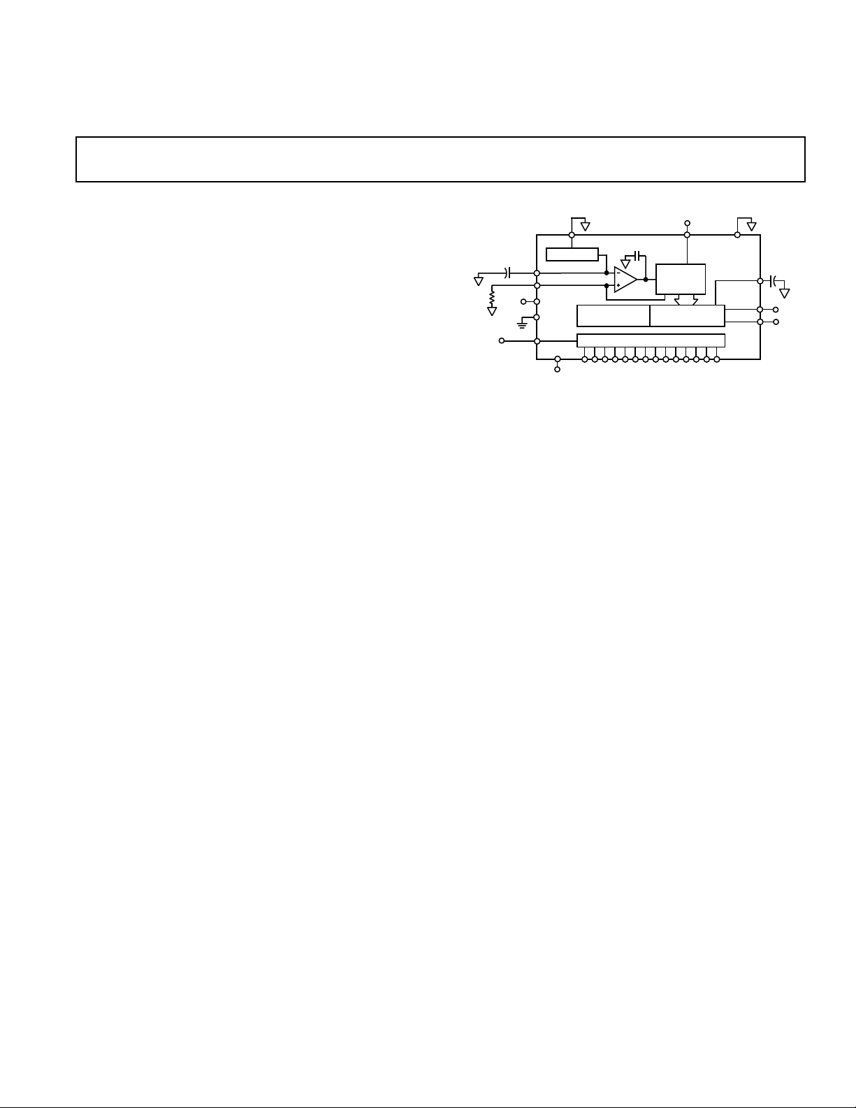
FUNCTIONAL BLOCK DIAGRAM
The AD9754 is a current-output DAC with a nominal full-scale
output current of 20 mA and > 100 kΩ output impedance.
Differential current outputs are provided to support singleended or differential applications. Matching between the two
current outputs ensures enhanced dynamic performance in a
differential output configuration. The current outputs may be
tied directly to an output resistor to provide two complementary, single-ended voltage outputs or fed directly into a transformer. The output voltage compliance range is 1.25 V.
The on-chip reference and control amplifier are configured for
maximum accuracy and flexibility. The AD9754 can be driven
by the on-chip reference or by a variety of external reference
voltages. The internal control amplifier, which provides a wide
(>10:1) adjustment span, allows the AD9754 full-scale current
to be adjusted over a 2 mA to 20 mA range while maintaining
excellent dynamic performance. Thus, the AD9754 may operate
at reduced power levels or be adjusted over a 20 dB range to
provide additional gain ranging capabilities.
The AD9754 is available in 28-lead SOIC and TSSOP packages.
It is specified for operation over the industrial temperature range.
PRODUCT HIGHLIGHTS
1. The AD9754 is a member of the wideband TxDAC high performance product family that provides an upward or downward
component selection path based on resolution (8 to 14 bits),
performance and cost. The entire family of TxDACs is available in industry standard pinouts.
2. Manufactured on a CMOS process, the AD9754 uses a
proprietary switching technique that enhances dynamic performance beyond that previously attainable by higher power/
cost bipolar or BiCMOS devices.
3. On-chip, edge-triggered input CMOS latches readily interface to +2.7 V to +5 V CMOS logic families. The AD9754
can support update rates up to 125 MSPS.
4. A flexible single-supply operating range of +4.5 V to +5.5 V,
and a wide full-scale current adjustment span of 2 mA to
20 mA, allows the AD9754 to operate at reduced power levels.
5. The current output(s) of the AD9754 can be easily configured for various single-ended or differential circuit topologies.
One Technology Way, P.O. Box 9106, Norwood, MA 02062-9106,U.S.A.
Tel: 781/329-4700 World Wide Web Site: http://www.analog.com
Fax: 781/326-8703 © Analog Devices, Inc., 1999
Page 2

AD9754–SPECIFICATIONS
(T
to T
DC SPECIFICATIONS
MIN
, AVDD = +5 V, DVDD = +5 V, I
MAX
Parameter Min Typ Max Units
RESOLUTION 14 Bits
DC ACCURACY
1
Integral Linearity Error (INL)
= +25°C –3.0 ±1.5 +3.0 LSB
T
A
Differential Nonlinearity (DNL)
T
= +25°C –2.0 ±0.75 +2.0 LSB
A
ANALOG OUTPUT
Offset Error –0.02 +0.02 % of FSR
Gain Error
Gain Error
Full-Scale Output Current
(Without Internal Reference) –2 ±0.5 +2 % of FSR
(With Internal Reference) –5 ±1.5 +5 % of FSR
2
2.0 20.0 mA
Output Compliance Range –1.0 1.25 V
Output Resistance 100 kΩ
Output Capacitance 5 pF
REFERENCE OUTPUT
Reference Voltage 1.14 1.20 1.26 V
Reference Output Current
3
REFERENCE INPUT
Input Compliance Range 0.1 1.25 V
Reference Input Resistance 1 MΩ
Small Signal Bandwidth 0.5 MHz
TEMPERATURE COEFFICIENTS
Offset Drift 0 ppm of FSR/°C
Gain Drift
Gain Drift
(Without Internal Reference) ±50 ppm of FSR/°C
(With Internal Reference) ±100 ppm of FSR/°C
Reference Voltage Drift ±50 ppm/°C
POWER SUPPLY
Supply Voltages
AVDD 4.5 5.0 5.5 V
DVDD 2.7 5.0 5.5 V
Analog Supply Current (I
Digital Supply Current (I
Supply Current Sleep Mode (I
Power Dissipation
5
(5 V, I
Power Supply Rejection Ratio
4
)
AVDD
5
)
DVDD
OUTFS
6
)
AVDD
= 20 mA) 185 220 mW
7
—AVDD –0.4 +0.4 % of FSR/V
Power Supply Rejection Ratio7—DVDD –0.025 +0.025 % of FSR/V
OPERATING RANGE –40 +85 °C
NOTES
1
Measured at IOUTA, driving a virtual ground.
2
Nominal full-scale current, I
3
Use an external buffer amplifier to drive any external load.
4
Requires +5 V supply.
5
Measured at f
6
Logic level for SLEEP pin must be referenced to AVDD. Min VIH = 3.5 V.
7
±5% Power supply variation.
Specifications subject to change without notice.
= 25 MSPS and I
CLOCK
, is 32 × the I
OUTFS
current.
REF
= static full scale (20 mA).
OUT
= 20 mA, unless otherwise noted)
OUTFS
100 nA
34 39 mA
3.0 5 mA
4.0 8 mA
–2–
REV. A
Page 3

AD9754
(T
to T
, AVDD = +5 V, DVDD = +5 V, I
MAX
DYNAMIC SPECIFICATIONS
MIN
50 ⍀ Doubly Terminated, unless otherwise noted)
Parameter Min Typ Max Units
DYNAMIC PERFORMANCE
Maximum Output Update Rate (f
Output Settling Time (t
Output Propagation Delay (t
) (to 0.1%)
ST
)1ns
PD
Glitch Impulse 5 pV-s
Output Rise Time (10% to 90%)
Output Fall Time (10% to 90%)
Output Noise (I
Output Noise (I
= 20 mA) 50 pA/√Hz
OUTFS
= 2 mA) 30 pA/√Hz
OUTFS
) 125 MSPS
CLOCK
1
1
1
AC LINEARITY
Spurious-Free Dynamic Range to Nyquist
f
= 25 MSPS; f
CLOCK
= 1.00 MHz
OUT
0 dBFS Output
= +25°C 75 86 dBc
T
A
–6 dBFS Output 86 dBc
–12 dBFS Output 78 dBc
= 50 MSPS; f
f
CLOCK
= 50 MSPS; f
f
CLOCK
= 50 MSPS; f
f
CLOCK
= 50 MSPS; f
f
CLOCK
= 100 MSPS; f
f
CLOCK
= 1.00 MHz 82 dBc
OUT
= 2.51 MHz 81 dBc
OUT
= 5.02 MHz 77 dBc
OUT
= 20.2 MHz 63 dBc
OUT
= 10 MHz 68 73 dBc
OUT
Spurious-Free Dynamic Range within a Window
= 25 MSPS; f
f
CLOCK
= 50 MSPS; f
f
CLOCK
= 100 MSPS; f
f
CLOCK
= 1.00 MHz; 2 MHz Span 84 93 dBc
OUT
= 5.02 MHz; 2 MHz Span 86 dBc
OUT
= 5.04 MHz; 4 MHz Span 86 dBc
OUT
Total Harmonic Distortion
= 25 MSPS; f
f
CLOCK
= +25°C –83 –75 dBc
T
A
= 50 MHz; f
f
CLOCK
= 100 MHz; f
f
CLOCK
= 1.00 MHz
OUT
= 2.00 MHz –78 dBc
OUT
= 2.00 MHz –78 dBc
OUT
Multitone Power Ratio (8 Tones at 110 kHz Spacing)
= 20 MSPS; f
f
CLOCK
= 2.00 MHz to 2.99 MHz
OUT
0 dBFS Output 85 dBc
–6 dBFS Output 84 dBc
–12 dBFS Output 87 dBc
–18 dBFS Output 88 dBc
NOTES
1
Measured single-ended into 50 Ω load.
Specifications subject to change without notice.
= 20 mA, Differential Transformer Coupled Output,
OUTFS
35 ns
2.5 ns
2.5 ns
REV. A
–3–
Page 4
AD9754
WARNING!
ESD SENSITIVE DEVICE
(T
to T
DIGITAL SPECIFICATIONS
MIN
, AVDD = +5 V, DVDD = +5 V, I
MAX
Parameter Min Typ Max Units
DIGITAL INPUTS
Logic “1” Voltage @ DVDD = +5 V
Logic “1” Voltage @ DVDD = +3 V 2.1 3 V
Logic “0” Voltage @ DVDD = +5 V
1
1
3.5 5 V
Logic “0” Voltage @ DVDD = +3 V 0 0.9 V
Logic “1” Current –10 +10 µA
Logic “0” Current –10 +10 µA
Input Capacitance 5 pF
Input Setup Time (t
Input Hold Time (t
Latch Pulsewidth (t
NOTES
1
When DVDD = +5 V and Logic 1 voltage ≈3.5 V and Logic 0 voltage ≈1.3 V, IVDD can increase by up to 10 mA depending on f
Specifications subject to change without notice.
) 2.0 ns
S
) 1.5 ns
H
) 3.5 ns
LPW
DB0–DB11
t
S
CLOCK
IOUTA
OR
IOUTB
t
PD
0.1%
t
LPW
t
ST
= 20 mA unless otherwise noted)
OUTFS
0 1.3 V
t
H
0.1%
CLOCK
.
Figure 1. Timing Diagram
ABSOLUTE MAXIMUM RATINGS*
With
Parameter Respect to Min Max Units
AVDD ACOM –0.3 +6.5 V
DVDD DCOM –0.3 +6.5 V
ACOM DCOM –0.3 +0.3 V
AVDD DVDD –6.5 +6.5 V
CLOCK, SLEEP DCOM –0.3 DVDD + 0.3 V
Model Range Descriptions Options*
AD9754AR –40°C to +85°C 28-Lead 300 Mil SOIC R-28
AD9754ARU –40°C to +85°C 28-Lead TSSOP RU-28
AD9754-EB Evaluation Board
*R = Small Outline IC; RU = Thin Shrink Small Outline Package.
Temperature Package Package
Digital Inputs DCOM –0.3 DVDD + 0.3 V
IOUTA, IOUTB ACOM –1.0 AVDD + 0.3 V
ICOMP ACOM –0.3 AVDD + 0.3 V
REFIO, FSADJ ACOM –0.3 AVDD + 0.3 V
REFLO ACOM –0.3 AVDD +0.3 V
Junction Temperature +150 °C
Storage Temperature –65 +150 °C
Lead Temperature
(10 sec) +300 °C
*Stresses above those listed under Absolute Maximum Ratings may cause perma-
nent damage to the device. This is a stress rating only; functional operation of the
device at these or any other conditions above those indicated in the operational
sections of this specification is not implied. Exposure to absolute maximum ratings
for extended periods may affect device reliability.
THERMAL CHARACTERISTICS
Thermal Resistance
28-Lead 300 Mil SOIC
= 71.4°C/W
θ
JA
= 23°C/W
θ
JC
28-Lead TSSOP
= 97.9°C/W
θ
JA
= 14.0°C/W
θ
JC
CAUTION
ESD (electrostatic discharge) sensitive device. Electrostatic charges as high as 4000 V readily
accumulate on the human body and test equipment and can discharge without detection.
Although the AD9754 features proprietary ESD protection circuitry, permanent damage may
occur on devices subjected to high energy electrostatic discharges. Therefore, proper ESD
precautions are recommended to avoid performance degradation or loss of functionality.
–4–
ORDERING GUIDE
REV. A
Page 5
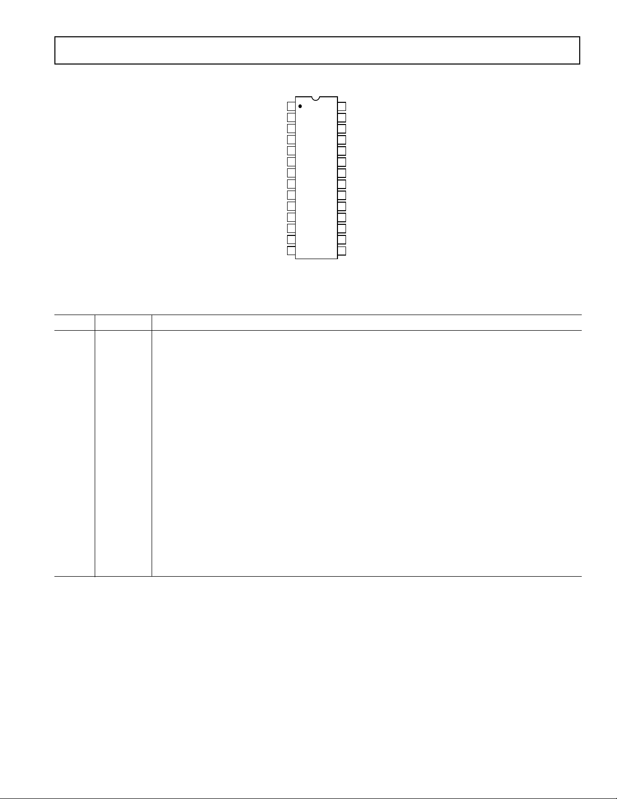
PIN CONFIGURATION
AD9754
(MSB) DB13
DB12
DB11
DB10
DB9
DB8
DB7
DB6
DB5
DB4
DB3
DB2
DB1
(LSB) DB0
1
2
3
4
5
AD9754
6
TOP VIEW
(Not to Scale)
7
8
9
10
11
12
13
14
NC = NO CONNECT
28
27
26
25
24
23
22
21
20
19
18
17
16
15
CLOCK
DVDD
DCOM
NC
AVDD
ICOMP
IOUTA
IOUTB
ACOM
NC
FS ADJ
REFIO
REFLO
SLEEP
PIN FUNCTION DESCRIPTIONS
Pin No. Name Description
1 DB13 Most Significant Data Bit (MSB).
2–13 DB12–DB1 Data Bits 1–12.
14 DB0 Least Significant Data Bit (LSB).
15 SLEEP Power-Down Control Input. Active High. Contains active pull-down circuit; it may be left unterminated if
not used.
16 REFLO Reference Ground when Internal 1.2 V Reference Used. Connect to AVDD to disable internal reference.
17 REFIO Reference Input/Output. Serves as reference input when internal reference disabled (i.e., Tie REFLO to
AVDD). Serves as 1.2 V reference output when internal reference activated (i.e., Tie REFLO to ACOM).
Requires 0.1 µF capacitor to ACOM when internal reference activated.
18 FS ADJ Full-Scale Current Output Adjust.
19, 25 NC No Connect.
20 ACOM Analog Common.
21 IOUTB Complementary DAC Current Output. Full-scale current when all data bits are 0s.
22 IOUTA DAC Current Output. Full-scale current when all data bits are 1s.
23 ICOMP Internal Bias Node for Switch Driver Circuitry. Decouple to ACOM with 0.1 µF capacitor.
24 AVDD Analog Supply Voltage (+4.5 V to +5.5 V).
26 DCOM Digital Common.
27 DVDD Digital Supply Voltage (+2.7 V to +5.5 V).
28 CLOCK Clock Input. Data latched on positive edge of clock.
REV. A
–5–
Page 6
AD9754
DEFINITIONS OF SPECIFICATIONS
Linearity Error (Also Called Integral Nonlinearity or INL)
Linearity error is defined as the maximum deviation of the
actual analog output from the ideal output, determined by a
straight line drawn from zero to full scale.
Differential Nonlinearity (or DNL)
DNL is the measure of the variation in analog value, normalized
to full scale, associated with a 1 LSB change in digital input
code.
Offset Error
The deviation of the output current from the ideal of zero is
called offset error. For IOUTA, 0 mA output is expected when
the inputs are all 0s. For IOUTB, 0 mA output is expected
when all inputs are set to 1s.
Gain Error
The difference between the actual and ideal output span. The
actual span is determined by the output when all inputs are set
to 1s minus the output when all inputs are set to 0s.
Output Compliance Range
The range of allowable voltage at the output of a current-output
DAC. Operation beyond the maximum compliance limits may
cause either output stage saturation or breakdown, resulting in
nonlinear performance.
Temperature Drift
Temperature drift is specified as the maximum change from the
ambient (+25°C) value to the value at either T
MIN
or T
MAX
. For
offset and gain drift, the drift is reported in ppm of full-scale
range (FSR) per °C. For reference drift, the drift is reported
in ppm per °C.
Power Supply Rejection
The maximum change in the full-scale output as the supplies
are varied over a specified range.
Settling Time
The time required for the output to reach and remain within a
specified error band about its final value, measured from the
start of the output transition.
Glitch Impulse
Asymmetrical switching times in a DAC give rise to undesired
output transients that are quantified by a glitch impulse. It is
specified as the net area of the glitch in pV-s.
Spurious-Free Dynamic Range
The difference, in dB, between the rms amplitude of the output
signal and the peak spurious signal over the specified bandwidth.
Total Harmonic Distortion
THD is the ratio of the sum of the rms value of the first six
harmonic components to the rms value of the measured output
signal. It is expressed as a percentage or in decibels (dB).
Multitone Power Ratio
The spurious-free dynamic range for an output containing multiple carrier tones of equal amplitude. It is measured as the
difference between the rms amplitude of a carrier tone to the
peak spurious signal in the region of a removed tone.
DVDD
DCOM
0.1mF
R
SET
2kV
50V
RETIMED
CLOCK
OUTPUT*
LECROY 9210
PULSE GENERATOR
+5V
+5V
REFIO
FS ADJ
DVDD
DCOM
CLOCK
SLEEP
REFLO
+1.20V REF
SEGMENTED SWITCHES
FOR DB13–DB5
CLOCK
OUTPUT
150pF
LATCHES
DIGITAL
DATA
TEKTRONIX AWG-2021
w/OPTION 4
AVDD ACOM
PMOS
CURRENT SOURCE
ARRAY
LSB
SWITCHES
AD9754
Figure 2. Basic AC Characterization Test Setup
ICOMP
IOUTA
IOUTB
50V
0.1mF
MINI-CIRCUITS
T1-1T
100V
50V
20pF
20pF
* AWG2021 CLOCK RETIMED
SUCH THAT DIGITAL DATA
TRANSITIONS ON FALLING EDGE
OF 50% DUTY CYCLE CLOCK.
TO HP3589A
SPECTRUM/
NETWORK
ANALYZER
50V INPUT
–6–
REV. A
Page 7
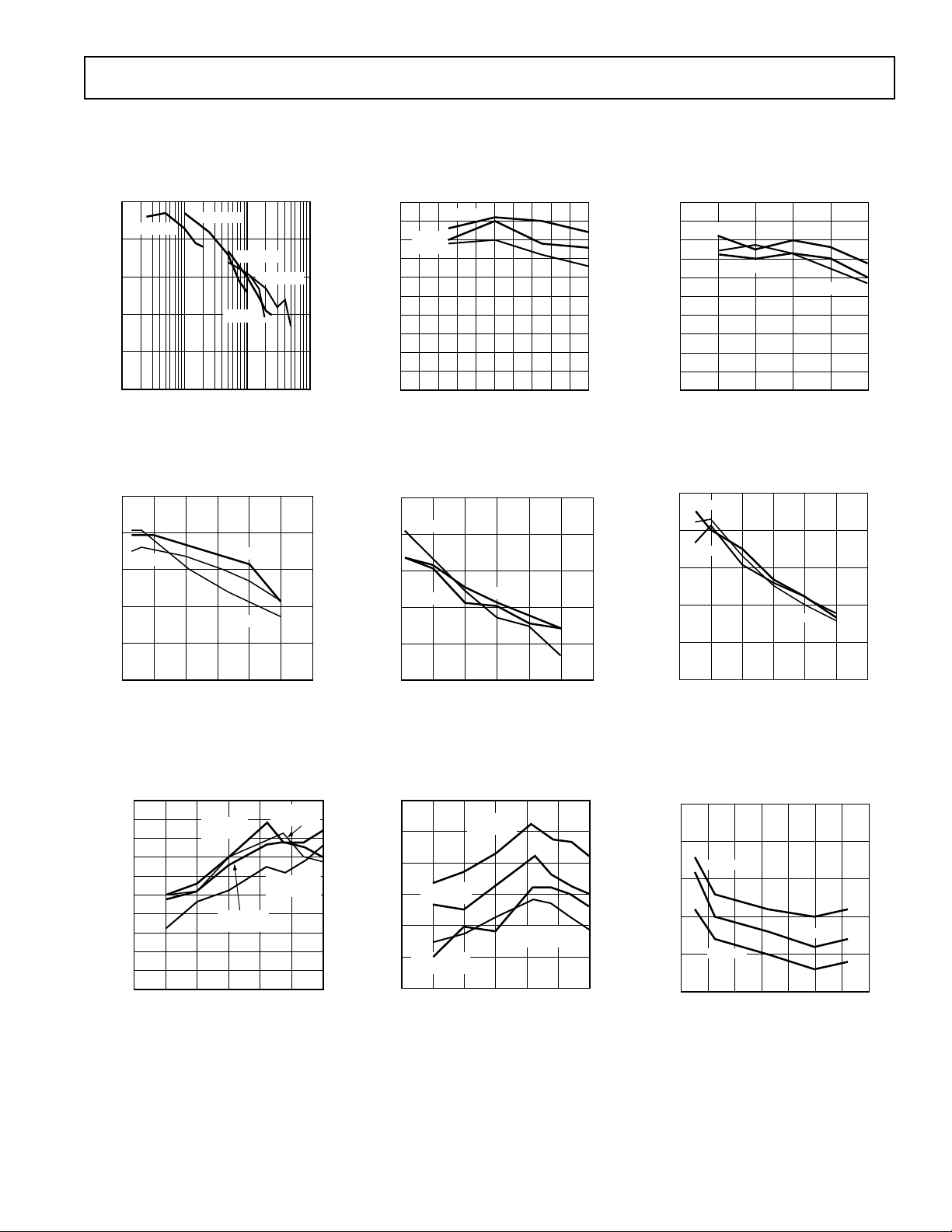
Typical AC Characterization Curves
FREQUENCY – MHz
SFDR – dB
90
95
02
46810
80
75
70
60
55
65
0dBFS
–6dBFS
–12dBFS
50
45
85
80
10mA FS
f
OUT
– MHz
SFDR – dBc
90
40
0
212
46810
60
50
70
20mA FS
5mA FS
f
CLOCK
– MSPS
SNR– dB
85
60
0 40 14060 80 100 120
80
70
75
65
20
20mA FS
5mA FS
10mA FS
(AVDD = +5 V, DVDD = +3 V, I
otherwise noted)
= 20 mA, 50 ⍀ Doubly Terminated Load, Differential Output, TA = +25ⴗC, SFDR up to Nyquist, unless
OUTFS
AD9754
90
5MSPS
80
70
60
SFDR – dB
50
40
0.1 100110
Figure 3. SFDR vs. f
90
80
–6dBFS
70
60
SFDR – dBc
50
25MSPS
f
– MHz
OUT
65MSPS
50MSPS
@ 0 dBFS
OUT
–12dBFS
0dBFS
125MSPS
90
85
80
75
70
65
60
SFDR – dB
55
50
45
40
0.0 2.00.4 0.8 1.2 1.6
Figure 4. SFDR vs. f
90
80
70
60
SFDR – dBc
50
0dBFS
–12dBFS
0dBFS
–12dBFS
–6dBFS
FREQUENCY – MHz
OUT
–6dBFS
@ 5 MSPS
Figure 5. SFDR vs. f
@ 25 MSPS
OUT
40
05 30
Figure 6. SFDR vs. f
90
85
80
75
70
65
60
SFDR – dB
55
50
45
40
–30 –25 0
Figure 9. Single-Tone SFDR vs. A
@ f
= f
OUT
REV. A
10 15 20
f
OUT
@5MSPS
–20 –15 –10 –5
A
OUT
/11
CLOCK
– MHz
@ 65 MSPS
OUT
455kHz
59.1MHz
@65MSPS
– dBFS
25
2.27MHz
@25MSPS
11.37MHz
@125MSPS
OUT
40
010 50
Figure 7. SFDR vs. f
100
90
80
70
SFDR – dB
60
50
40
–30 –25 0
20 30 40
f
OUT
@5MSPS
5MHz
@25MSPS
13MHz
@65MSPS
–20 –15 –10 –5
A
OUT
– MHz
OUT
1MHz
– dBFS
@125 MSPS
25MHz
@125MSPS
Figure 10. Single-Tone SFDR vs.
A
@ f
OUT
OUT
= f
CLOCK
/5
–7–
60
Figure 8. SFDR vs. f
I
@ 25 MSPS and 0 dBFS
OUTFS
Figure 11. SNR vs. f
@ f
= 2 MHz and 0 dBFS
OUT
OUT
CLOCK
and
and I
OUTFS
Page 8
AD9754
1.0
0.5
0
–0.5
ERROR – LSB
–1.0
–1.5
–2.0
0
4k 8k 12k
CODE
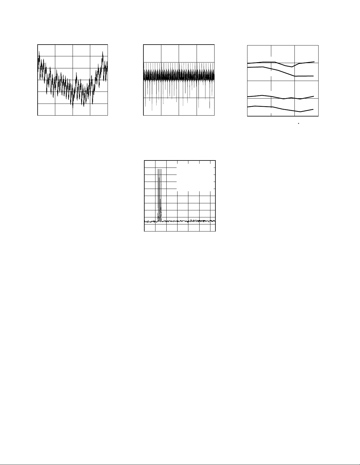
Figure 12. Typical INL
16k
1.0
0.5
0
ERROR – LSB
–0.5
–1.0
4k 8k 12k
0
CODE
Figure 13. Typical DNL
16k
90
80
70
SFDR – dBc
60
50
–55 –5 95
Figure 14. SFDR vs. Temperature @
125 MSPS, 0 dBFS
0
–10
–20
–30
–40
–50
–60
–70
–80
SINGLE AMPLITUDE – dBm
–90
–100
030
f
= 65MSPS
CLOCK
f
= 6.25MHz
OUT1
f
= 6.75MHz
OUT2
f
= 7.25MHz
OUT3
f
= 7.75MHz
OUT4
SFDR > 70dBc
AMPLITUDE = 0dBFS
FREQUENCY – MHz
252015105
Figure 15. Four-Tone SFDR
f
OUT
f
= 10MHz
OUT
f
OUT
f
= 40MHz
OUT
TEMPERATURE – C
= 4MHz
= 29MHz
45
–8–
REV. A
Page 9

AD9754
)
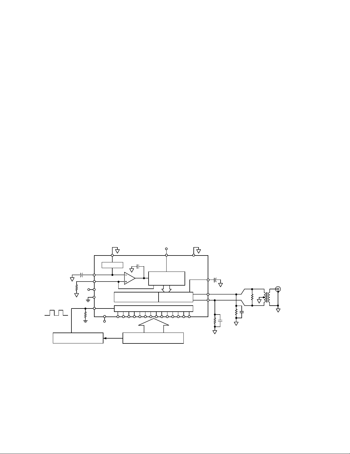
FUNCTIONAL DESCRIPTION
Figure 16 shows a simplified block diagram of the AD9754. The
AD9754 consists of a large PMOS current source array that is
capable of providing up to 20 mA of total current. The array
is divided into 31 equal currents that make up the five most
significant bits (MSBs). The next four bits or middle bits consist
of 15 equal current sources whose value is 1/16th of an MSB
current source. The remaining LSBs are binary weighted fractions of the middle bits current sources. Implementing the
middle and lower bits with current sources, instead of an R-2R
ladder, enhances its dynamic performance for multitone or low
amplitude signals and helps maintain the DAC’s high output
impedance (i.e., >100 kΩ).
All of these current sources are switched to one or the other of
the two output nodes (i.e., IOUTA or IOUTB) via PMOS
differential current switches. The switches are based on a new
architecture that drastically improves distortion performance.
This new switch architecture reduces various timing errors and
provides matching complementary drive signals to the inputs of
the differential current switches.
The analog and digital sections of the AD9754 have separate
power supply inputs (i.e., AVDD and DVDD). The digital section, which is capable of operating up to a 125 MSPS clock rate
and over +2.7 V to +5.5 V operating range, consists of edgetriggered latches and segment decoding logic circuitry. The
analog section, which can operate over a +4.5 V to +5.5 V range
includes the PMOS current sources, the associated differential
switches, a 1.20 V bandgap voltage reference and a reference
control amplifier.
The full-scale output current is regulated by the reference control amplifier and can be set from 2 mA to 20 mA via an external resistor, R
both the reference control amplifier and voltage reference V
sets the reference current I
. The external resistor, in combination with
SET
, which is mirrored over to the
REF
REFIO
,
segmented current sources with the proper scaling factor. The
full-scale current, I
, is 32 times the value of I
OUTFS
REF
.
DAC TRANSFER FUNCTION
The AD9754 provides complementary current outputs, IOUTA
and IOUTB. IOUTA will provide a near full-scale current output, I
, when all bits are high (i.e., DAC CODE = 16383)
OUTFS
while IOUTB, the complementary output, provides no current.
The current output appearing at IOUTA and IOUTB is a function of both the input code and I
IOUTA = (DAC CODE/16384) × I
IOUTB = (16383 – DAC CODE)/16384 × I
and can be expressed as:
OUTFS
OUTFS
OUTFS
(1)
(2)
where DAC CODE = 0 to 16383 (i.e., Decimal Representation).
As mentioned previously, I
current I
and external resistor R
where I
, which is nominally set by a reference voltage V
REF
SET
I
= 32 × I
OUTFS
REF
= V
REF
REFIO/RSET
is a function of the reference
OUTFS
. It can be expressed as:
REFIO
(3)
(4)
The two current outputs will typically drive a resistive load
directly or via a transformer. If dc coupling is required, IOUTA
and IOUTB should be directly connected to matching resistive
loads, R
that R
, that are tied to analog common, ACOM. Note
LOAD
may represent the equivalent load resistance seen by
LOAD
IOUTA or IOUTB as would be the case in a doubly terminated
50 Ω or 75 Ω cable. The single-ended voltage output appearing
at the IOUTA and IOUTB nodes is simply:
V
= IOUTA × R
OUTA
V
= IOUTB × R
OUTB
Note that the full-scale value of V
LOAD
LOAD
OUTA
and V
should not
OUTB
(5)
(6)
exceed the specified output compliance range to maintain specified distortion and linearity performance.
The differential voltage, V
, appearing across IOUTA and
DIFF
IOUTB is:
V
= (IOUTA – IOUTB) × R
DIFF
Substituting the values of IOUTA, IOUTB and I
LOAD
REF
; V
DIFF
(7)
can
be expressed as:
V
= {(2 DAC CODE – 16383)/16384} ×
DIFF
V
DIFF
= {(32 R
LOAD/RSET
) × V
REFIO
(8)
REV. A
0.1mF
V
REFIO
R
CLOCK
SET
2kV
I
+5V
REF
+5V
REFIO
FS ADJ
DVDD
DCOM
CLOCK
SLEEP
REFLO
+1.20V REF
SEGMENTED SWITCHES
FOR DB13–DB5
DIGITAL DATA INPUTS (DB13–DB0
150pF
LATCHES
AVDD ACOM
PMOS
CURRENT SOURCE
ARRAY
SWITCHES
Figure 16. Functional Block Diagram
–9–
LSB
AD9754
ICOMP
IOUTA
IOUTB
0.1mF
I
OUTB
I
OUTA
V
= V
OUTB
LOAD
OUTA
– V
OUTB
V
OUTA
R
50V
LOAD
DIFF
V
R
50V
Page 10

AD9754
150pF
+1.2V REF
AVDDREFLO
CURRENT
SOURCE
ARRAY
AVDD
REFIO
FS ADJ
R
SET
AD9754
EXTERNAL
REF
I
REF
=
V
REFIO/RSET
AVDD
REFERENCE
CONTROL
AMPLIFIER
V
REFIO
These last two equations highlight some of the advantages of
operating the AD9754 differentially. First, the differential operation will help cancel common-mode error sources associated
with IOUTA and IOUTB such as noise, distortion and dc offsets. Second, the differential code-dependent current and
subsequent voltage, V
ended voltage output (i.e., V
, is twice the value of the single-
DIFF
OUTA
or V
), thus providing
OUTB
twice the signal power to the load.
Note that the gain drift temperature performance for a singleended (VOUTA and VOUTB) or differential output (V
DIFF
) of
the AD9754 can be enhanced by selecting temperature tracking
resistors for R
LOAD
and R
due to their ratiometric relation-
SET
ship as shown in Equation 8.
REFERENCE OPERATION
The AD9754 contains an internal 1.20 V bandgap reference
that can be easily disabled and overridden by an external
reference. REFIO serves as either an input or output, depending
on whether the internal or external reference is selected. If
REFLO is tied to ACOM, as shown in Figure 17, the internal
reference is activated, and REFIO provides a 1.20 V output. In
this case, the internal reference must be compensated externally
with a ceramic chip capacitor of 0.1 µF or greater from REFIO
to REFLO. Also, REFIO should be buffered with an external
amplifier having an input bias current less than 100 nA if any
additional loading is required.
+5V
OPTIONAL
ADDITIONAL
LOAD
EXTERNAL
REF BUFFER
0.1mF
2kV
REFIO
FS ADJ
AD9754
REFLO
+1.2V REF
150pF
AVDD
CURRENT
SOURCE
ARRAY
Figure 17. Internal Reference Configuration
The internal reference can be disabled by connecting REFLO to
AVDD. In this case, an external reference may then be applied
to REFIO as shown in Figure 18. The external reference may
provide either a fixed reference voltage to enhance accuracy and
drift performance or a varying reference voltage for gain control.
Note that the 0.1 µF compensation capacitor is not required
since the internal reference is disabled, and the high input im-
pedance (i.e., 1 MΩ) of REFIO minimizes any loading of the
external reference.
REFERENCE CONTROL AMPLIFIER
The AD9754 also contains an internal control amplifier that is
used to regulate the DAC’s full-scale output current, I
OUTFS
.
The control amplifier is configured as a V-I converter, as shown
in Figure 18, such that its current output, I
, is determined by
REF
Figure 18. External Reference Configuration
the ratio of the V
in Equation 4. I
sources with the proper scaling factor to set I
and an external resistor, R
REFIO
is copied over to the segmented current
REF
SET
OUTFS
, as stated
as stated in
Equation 3.
The control amplifier allows a wide (10:1) adjustment span of
I
over a 2 mA to 20 mA range by setting IREF between
OUTFS
62.5 µA and 625 µA. The wide adjustment span of I
OUTFS
provides several application benefits. The first benefit relates
directly to the power dissipation of the AD9754, which is proportional to I
(refer to the Power Dissipation section). The
OUTFS
second benefit relates to the 20 dB adjustment, which is useful
for system gain control purposes.
The small signal bandwidth of the reference control amplifier
is approximately 0.5 MHz. The output of the control amplifier
is internally compensated via a 150 pF capacitor that limits the
control amplifier small-signal bandwidth and reduces its output
impedance. Since the –3 dB bandwidth corresponds to the
dominant pole, and hence the time constant, the settling time of
the control amplifier to a stepped reference input response can
be approximated In this case, the time constant can be approximated to be 320 ns.
There are two methods in which I
. The first method is suitable for a single-supply system in
R
SET
can be varied for a fixed
REF
which the internal reference is disabled, and the common-mode
voltage of REFIO is varied over its compliance range of 1.25 V
to 0.10 V. REFIO can be driven by a single-supply amplifier or
DAC, thus allowing I
to be varied for a fixed R
REF
. Since the
SET
AVDD
V
1.2V
AD1580
R
OUT1
AD7524
OUT2
AGND
Figure 19. Single-Supply Gain Control Circuit
FB
DD
V
REF
DB7–DB0
0.1V TO 1.2V
R
SET
–10–
I
=
REF
V
REF/RSET
+1.2V REF
REFIO
FS ADJ
AD9754
150pF
AVDD
AVDDREFLO
CURRENT
SOURCE
ARRAY
REV. A
Page 11

input impedance of REFIO is approximately 1 MΩ, a simple,
AD9754
AVDD
IOUTA IOUTB
R
LOAD
R
LOAD
low cost R-2R ladder DAC configured in the voltage mode
topology may be used to control the gain. This circuit is shown
in Figure 19 using the AD7524 and an external 1.2 V reference,
the AD1580.
The second method may be used in a dual-supply system in
which the common-mode voltage of REFIO is fixed, and I
varied by an external voltage, V
GC
, applied to R
via an ampli-
SET
REF
is
fier. An example of this method is shown in Figure 25 in which
the internal reference is used to set the common-mode voltage
of the control amplifier to 1.20 V. The external voltage, V
GC
, is
referenced to ACOM and should not exceed 1.2 V. The value of
is such that I
R
SET
REFMAX
and I
do not exceed 62.5 µA
REFMIN
and 625 µA, respectively. The associated equations in Figure 20
can be used to determine the value of R
+1.2V REF
REFIO
1mF
R
SET
V
GC
FS ADJ
I
REF
AD9754
I
= (1.2 – VGC)/R
REF
WITH V
GC
V
REFIO
.
SET
150pF
SET
AND 62.5mA I
AVDD
AVDDREFLO
CURRENT
SOURCE
ARRAY
625A
REF
Figure 20. Dual-Supply Gain Control Circuit
ANALOG OUTPUTS
The AD9754 produces two complementary current outputs,
IOUTA and IOUTB, which may be configured for single-end
or differential operation. IOUTA and IOUTB can be converted
into complementary single-ended voltage outputs, V
, via a load resistor, R
V
OUTB
, as described in the DAC
LOAD
OUTA
and
Transfer Function section by Equations 5 through 8. The
differential voltage, V
, existing between V
DIFF
OUTA
and V
OUTB
can also be converted to a single-ended voltage via a transformer
or differential amplifier configuration.
Figure 21 shows the equivalent analog output circuit of the
AD9754 consisting of a parallel combination of PMOS differential current switches associated with each segmented current
source. The output impedance of IOUTA and IOUTB is determined by the equivalent parallel combination of the PMOS
switches and is typically 100 kΩ in parallel with 5 pF. Due to
the nature of a PMOS device, the output impedance is also
slightly dependent on the output voltage (i.e., V
OUTA
and V
OUTB
)
and, to a lesser extent, the analog supply voltage, AVDD, and
full-scale current, I
. Although the output impedance’s signal
OUTFS
dependency can be a source of dc nonlinearity and ac linearity
(i.e., distortion), its effects can be limited if certain precautions
are noted.
AD9754
Figure 21. Equivalent Analog Output Circuit
IOUTA and IOUTB also have a negative and positive voltage
compliance range. The negative output compliance range of
–1.0 V is set by the breakdown limits of the CMOS process.
Operation beyond this maximum limit may result in a breakdown of the output stage and affect the reliability of the AD9754.
The positive output compliance range is slightly dependent on
the full-scale output current, I
nominal 1.25 V for an I
= 20 mA to 1.00 V for an I
OUTFS
2 mA. Operation beyond the positive compliance range will
induce clipping of the output signal which severely degrades
the AD9754’s linearity and distortion performance.
For applications requiring the optimum dc linearity, IOUTA
and/or IOUTB should be maintained at a virtual ground via an
I-V op amp configuration. Maintaining IOUTA and/or IOUTB
at a virtual ground keeps the output impedance of the AD9754
fixed, significantly reducing its effect on linearity. However,
it does not necessarily lead to the optimum distortion performance due to limitations of the I-V op amp. Note that the
INL/DNL specifications for the AD9754 are measured in
this manner using IOUTA. In addition, these dc linearity
specifications remain virtually unaffected over the specified
power supply range of +4.5 V to +5.5 V.
Operating the AD9754 with reduced voltage output swings at
IOUTA and IOUTB in a differential or single-ended output
configuration reduces the signal dependency of its output
impedance thus enhancing distortion performance. Although
the voltage compliance range of IOUTA and IOUTB extends
from –1.0 V to +1.25 V, optimum distortion performance is
achieved when the maximum full-scale signal at IOUTA and
IOUTB does not exceed approximately 0.5 V. A properly selected transformer with a grounded center-tap will allow the
AD9754 to provide the required power and voltage levels to
different loads while maintaining reduced voltage swings at
IOUTA and IOUTB. DC-coupled applications requiring a
differential or single-ended output configuration should size
accordingly. Refer to Applying the AD9754 section for
R
LOAD
examples of various output configurations.
. It degrades slightly from its
OUTFS
OUTFS
=
REV. A
–11–
Page 12

AD9754
The most significant improvement in the AD9754’s distortion
and noise performance is realized using a differential output
configuration. The common-mode error sources of both
IOUTA and IOUTB can be substantially reduced by the
common-mode rejection of a transformer or differential amplifier. These common-mode error sources include even-order
distortion products and noise. The enhancement in distortion
performance becomes more significant as the reconstructed
waveform’s frequency content increases and/or its amplitude
decreases.
The distortion and noise performance of the AD9754 is also
slightly dependent on the analog and digital supply as well as the
full-scale current setting, I
. Operating the analog supply at
OUTFS
5.0 V ensures maximum headroom for its internal PMOS current
sources and differential switches leading to improved distortion
performance. Although I
20 mA, selecting an I
can be set between 2 mA and
OUTFS
of 20 mA will provide the best
OUTFS
distortion and noise performance also shown in Figure 13. The
noise performance of the AD9754 is affected by the digital supply (DVDD), output frequency, and increases with increasing
clock rate as shown in Figure 8. Operating the AD9754 with
low voltage logic levels between 3 V and 3.3 V will slightly
reduce the amount of on-chip digital noise.
In summary, the AD9754 achieves the optimum distortion and
noise performance under the following conditions:
(1) Differential Operation.
(2) Positive voltage swing at IOUTA and IOUTB limited to
+0.5 V.
(3) I
set to 20 mA.
OUTFS
(4) Analog Supply (AVDD) set at 5.0 V.
(5) Digital Supply (DVDD) set at 3.0 V to 3.3 V with appro-
priate logic levels.
Note that the ac performance of the AD9754 is characterized
under the above mentioned operating conditions.
DIGITAL INPUTS
The AD9754’s digital input consists of 14 data input pins and a
clock input pin. The 14-bit parallel data inputs follow standard
positive binary coding where DB13 is the most significant bit
(MSB), and DB0 is the least significant bit (LSB). IOUTA
produces a full-scale output current when all data bits are at
Logic 1. IOUTB produces a complementary output with the
full-scale current split between the two outputs as a function of
the input code.
The digital interface is implemented using an edge-triggered
master slave latch. The DAC output is updated following the
rising edge of the clock as shown in Figure 1 and is designed to
support a clock rate as high as 125 MSPS. The clock can be
operated at any duty cycle that meets the specified latch pulse
width. The setup and hold times can also be varied within the
clock cycle as long as the specified minimum times are met,
although the location of these transition edges may affect digital
feedthrough and distortion performance. Best performance is
typically achieved when the input data transitions on the falling
edge of a 50% duty cycle clock.
The digital inputs are CMOS-compatible with logic thresholds,
V
THRESHOLD,
set to approximately half the digital positive supply
(DVDD) or
V
THRESHOLD
= DVDD/2 (±20%)
The internal digital circuitry of the AD9754 is capable of operating
over a digital supply range of 2.7 V to 5.5 V. As a result, the
digital inputs can also accommodate TTL levels when DVDD is
set to accommodate the maximum high level voltage of the TTL
drivers V
OH(MAX)
. A DVDD of 3 V to 3.3 V will typically ensure
proper compatibility with most TTL logic families. Figure 22
shows the equivalent digital input circuit for the data and clock
inputs. The sleep mode input is similar with the exception that
it contains an active pull-down circuit, thus ensuring that the
AD9754 remains enabled if this input is left disconnected.
DVDD
DIGITAL
INPUT
Figure 22. Equivalent Digital Input
Since the AD9754 is capable of being updated up to 125 MSPS,
the quality of the clock and data input signals are important in
achieving the optimum performance. Operating the AD9754
with reduced logic swings and a corresponding digital supply
(DVDD) will result in the lowest data feedthrough and on-chip
digital noise. The drivers of the digital data interface circuitry
should be specified to meet the minimum setup and hold times
of the AD9754 as well as its required min/max input logic level
thresholds.
Digital signal paths should be kept short and run lengths
matched to avoid propagation delay mismatch. The insertion of
a low value resistor network (i.e., 20 Ω to 100 Ω) between the
AD9754 digital inputs and driver outputs may be helpful in
reducing any overshooting and ringing at the digital inputs that
contribute to data feedthrough. For longer run lengths and high
data update rates, strip line techniques with proper termination
resistors should be considered to maintain “clean” digital inputs.
The external clock driver circuitry should provide the AD9754
with a low jitter clock input meeting the min/max logic levels
while providing fast edges. Fast clock edges will help minimize
any jitter that will manifest itself as phase noise on a reconstructed waveform. Thus, the clock input should be driven by
the fastest logic family suitable for the application.
Note, that the clock input could also be driven via a sine wave,
which is centered around the digital threshold (i.e., DVDD/2)
and meets the min/max logic threshold. This will typically result
in a slight degradation in the phase noise, which becomes more
noticeable at higher sampling rates and output frequencies.
Also, at higher sampling rates, the 20% tolerance of the digital
logic threshold should be considered since it will affect the effective clock duty cycle and, subsequently, cut into the required
data setup and hold times.
–12–
REV. A
Page 13

INPUT CLOCK AND DATA TIMING RELATIONSHIP
I
OUTFS
– mA
35
5
2204 6 8 10 12 14 16 18
30
25
20
15
10
I
AVDD
– mA
RATIO (f
CLOCK/fOUT
)
8
0
0.01 10.1
I
DVDD
– mA
6
4
2
5MSPS
25MSPS
50MSPS
100MSPS
125MSPS
SNR in a DAC is dependent on the relationship between the
position of the clock edges and the point in time at which the
input data changes. The AD9754 is positive edge triggered, and
so exhibits SNR sensitivity when the data transition is close to
this edge. In general, the goal when applying the AD9754 is to
make the data transitions close to the negative clock edge. This
becomes more important as the sample rate increases. Figure 23
shows the relationship of SNR to clock placement.
68
FS = 65MSPS
64
60
AD9754
56
52
SNR – dB
48
44
40
–8
–6 –4 –2
TIME (ns) OF DATA CHANGE RELATIVE TO
0
RISING CLOCK EDGE
Figure 23. SNR vs. Clock Placement @ f
FS = 125MSPS
246810
= 10 MHz
OUT
SLEEP MODE OPERATION
The AD9754 has a power-down function that turns off the
output current and reduces the supply current to less than
8.5 mA over the specified supply range of 2.7 V to 5.5 V and
temperature range. This mode can be activated by applying a
logic level “1” to the SLEEP pin. This digital input also con-
Figure 24. I
18
16
14
12
10
– mA
8
DVDD
I
6
4
2
0
0.01 10.1
Figure 25. I
RATIO (f
vs. Ratio @ DVDD = 5 V
DVDD
vs. I
AVDD
CLOCK/fOUT
OUTFS
125MSPS
100MSPS
50MSPS
25MSPS
5MSPS
)
tains an active pull-down circuit that ensures the AD9754 remains enabled if this input is left disconnected. The AD9754
takes less than 50 ns to power down and approximately 5 µs to
power back up.
POWER DISSIPATION
The power dissipation, PD, of the AD9754 is dependent on
several factors, including: (1) AVDD and DVDD, the power
supply voltages; (2) I
, the update rate; and (4) the reconstructed digital input
f
CLOCK
, the full-scale current output; (3)
OUTFS
waveform. The power dissipation is directly proportional to the
analog supply current, I
. I
I
DVDD
is directly proportional to I
AVDD
Figure 24, and is insensitive to f
Conversely, I
form, f
CLOCK
show I
DVDD
(f
OUT/fCLOCK
DVDD = 3 V, respectively. Note, how I
than a factor of 2 when DVDD is reduced from 5 V to 3 V.
is dependent on both the digital input wave-
DVDD
, and digital supply DVDD. Figures 25 and 26
as a function of full-scale sine wave output ratios
) for various update rates with DVDD = 5 V and
, and the digital supply current,
AVDD
CLOCK
.
DVDD
as shown in
OUTFS,
is reduced by more
Figure 26. I
vs. Ratio @ DVDD = 3 V
DVDD
REV. A
–13–
Page 14

AD9754
AD9754
22
IOUTA
IOUTB
21
C
OPT
500V
225V
225V
1kV
25V25V
AD8041
1kV
AVDD
APPLYING THE AD9754
OUTPUT CONFIGURATIONS
The following sections illustrate some typical output configurations for the AD9754. Unless otherwise noted, it is assumed
that I
is set to a nominal 20 mA. For applications requir-
OUTFS
ing the optimum dynamic performance, a differential output
configuration is suggested. A differential output configuration
may consist of either an RF transformer or a differential op amp
configuration. The transformer configuration provides the optimum high frequency performance and is recommended for any
application allowing for ac coupling. The differential op amp
configuration is suitable for applications requiring dc coupling, a
bipolar output, signal gain and/or level shifting.
A single-ended output is suitable for applications requiring a
unipolar voltage output. A positive unipolar output voltage will
result if IOUTA and/or IOUTB is connected to an appropriately sized load resistor, R
, referred to ACOM. This con-
LOAD
figuration may be more suitable for a single-supply system
requiring a dc coupled, ground referred output voltage. Alternatively, an amplifier could be configured as an I-V converter, thus
converting IOUTA or IOUTB into a negative unipolar voltage.
This configuration provides the best dc linearity since IOUTA
or IOUTB is maintained at a virtual ground. Note, IOUTA
provides slightly better performance than IOUTB.
DIFFERENTIAL COUPLING USING A TRANSFORMER
An RF transformer can be used to perform a differential-tosingle-ended signal conversion as shown in Figure 27. A
differentially coupled transformer output provides the optimum
distortion performance for output signals whose spectral content
lies within the transformer’s passband. An RF transformer such
as the Mini-Circuits T1-1T provides excellent rejection of
common-mode distortion (i.e., even-order harmonics) and noise
over a wide frequency range. It also provides electrical isolation
and the ability to deliver twice the power to the load. Transformers with different impedance ratios may also be used for
impedance matching purposes. Note that the transformer
provides ac coupling only.
MINI-CIRCUITS
IOUTA
AD9754
IOUTB
22
21
T1-1T
OPTIONAL R
DIFF
R
LOAD
DIFFERENTIAL USING AN OP AMP
An op amp can also be used to perform a differential-to-singleended conversion as shown in Figure 28. The AD9754 is configured with two equal load resistors, R
, of 25 Ω. The
LOAD
differential voltage developed across IOUTA and IOUTB is
converted to a single-ended signal via the differential op amp
configuration. An optional capacitor can be installed across
IOUTA and IOUTB, forming a real pole in a low-pass filter.
The addition of this capacitor also enhances the op amp’s distortion performance by preventing the DAC’s high slewing
output from overloading the op amp’s input.
The common-mode rejection of this configuration is typically
determined by the resistor matching. In this circuit, the differential op amp circuit is configured to provide some additional
signal gain. The op amp must operate from a dual supply since
its output is approximately ±1.0 V. A high speed amplifier such
as the AD8055 or AD9632 capable of preserving the differential
500V
AD9754
IOUTA
IOUTB
22
21
C
OPT
225V
225V
25V25V
AD8055
500V
Figure 28. DC Differential Coupling Using an Op Amp
performance of the AD9754 while meeting other system level
objectives (i.e., cost, power) should be selected. The op amps
differential gain, its gain setting resistor values and full-scale
output swing capabilities should all be considered when optimizing this circuit.
The differential circuit shown in Figure 29 provides the necessary level-shifting required in a single supply system. In this
case, AVDD, which is the positive analog supply for both the
AD9754 and the op amp, is also used to level-shift the differential output of the AD9754 to midsupply (i.e., AVDD/2). The
AD8041 is a suitable op amp for this application.
Figure 27. Differential Output Using a Transformer
The center tap on the primary side of the transformer must be
connected to ACOM to provide the necessary dc current path
for both IOUTA and IOUTB. The complementary voltages
appearing at IOUTA and IOUTB (i.e., V
OUTA
and V
OUTB
swing symmetrically around ACOM and should be maintained
with the specified output compliance range of the AD9754. A
differential resistor, R
, may be inserted in applications in
DIFF
which the output of the transformer is connected to the load,
, via a passive reconstruction filter or cable. R
R
LOAD
mined by the transformer’s impedance ratio and provides the
proper source termination that results in a low VSWR. Note
that approximately half the signal power will be dissipated
across R
DIFF
.
DIFF
)
is deter-
Figure 29. Single-Supply DC Differential Coupled Circuit
–14–
REV. A
Page 15

AD9754
FREQUENCY – MHz
PSRR – dB
90
60
1.00.5 0.75
80
70
0.26
SINGLE-ENDED UNBUFFERED VOLTAGE OUTPUT
Figure 30 shows the AD9754 configured to provide a unipolar
output range of approximately 0 V to +0.5 V for a doubly termi-
nated 50 Ω cable since the nominal full-scale current, I
20 mA flows through the equivalent R
represents the equivalent load resistance seen by IOUTA
R
LOAD
of 25 Ω. In this case,
LOAD
OUTFS
, of
or IOUTB. The unused output (IOUTA or IOUTB) can be
connected to ACOM directly or via a matching R
values of I
OUTFS
and R
can be selected as long as the posi-
LOAD
LOAD
. Different
tive compliance range is adhered to. One additional consideration in this mode is the integral nonlinearity (INL) as discussed
in the Analog Output section of this data sheet. For optimum
INL performance, the single-ended, buffered voltage output
configuration is suggested.
POWER AND GROUNDING CONSIDERATIONS, POWER
SUPPLY REJECTION
Many applications seek high speed and high performance under
less than ideal operating conditions. In these circuits, the implementation and construction of the printed circuit board design
is as important as the circuit design. Proper RF techniques must
be used for device selection, placement and routing as well as
power supply bypassing and grounding to ensure optimum
performance. Figures 39-44 illustrate the recommended printed
circuit board ground, power and signal plane layouts which are
implemented on the AD9754 evaluation board.
One factor that can measurably affect system performance is the
ability of the DAC output to reject dc variations or ac noise
superimposed on the analog or digital dc power distribution
(i.e., AVDD, DVDD). This is referred to as Power Supply
AD9754
IOUTA
IOUTB
I
= 20mA
OUTFS
22
50V
21
25V
V
OUTA
= 0 TO +0.5V
50V
Rejection Ratio (PSRR). For dc variations of the power supply,
the resulting performance of the DAC directly corresponds to a
gain error associated with the DAC’s full-scale current, I
OUTFS
.
AC noise on the dc supplies is common in applications where
the power distribution is generated by a switching power supply.
Typically, switching power supply noise will occur over the
spectrum from tens of kHz to several MHz. PSRR vs. frequency
Figure 30. 0 V to +0.5 V Unbuffered Voltage Output
of the AD9754 AVDD supply, over this frequency range, is
given in Figure 32.
SINGLE-ENDED BUFFERED VOLTAGE OUTPUT
CONFIGURATION
Figure 31 shows a buffered single-ended output configuration in
which the op amp U1 performs an I-V conversion on the AD9754
output current. U1 maintains IOUTA (or IOUTB) at a virtual
ground, thus minimizing the nonlinear output impedance effect
on the DAC’s INL performance as discussed in the Analog
Output section. Although this single-ended configuration typically provides the best dc linearity performance, its ac distortion
performance at higher DAC update rates may be limited by
U1’s slewing capabilities. U1 provides a negative unipolar
output voltage and its full-scale output voltage is simply the
product of R
and I
FB
within U1’s voltage output swing capabilities by scaling I
. The full-scale output should be set
OUTFS
OUTFS
and/or RFB. An improvement in ac distortion performance may
result with a reduced I
required to sink will be subsequently reduced.
AD9754
IOUTA
IOUTB
I
OUTFS
22
21
Figure 31. Unipolar Buffered Voltage Output
since the signal current U1 will be
OUTFS
C
OPT
R
FB
= 10mA
200V
200V
U1
V
= I
OUT
OUTFS
3 R
Figure 32. Power Supply Rejection Ratio of AD9754
Note that the units in Figure 32 are given in units of (amps out)/
(volts in). Noise on the analog power supply has the effect of
modulating the internal switches, and therefore the output
current. The voltage noise on the dc power, therefore, will be
added in a nonlinear manner to the desired I
. Due to the
OUT
relative different sizes of these switches, PSRR is very code
FB
dependent. This can produce a mixing effect which can modulate low frequency power supply noise to higher frequencies.
Worst case PSRR for either one of the differential DAC outputs
will occur when the full-scale current is directed towards that
output. As a result, the PSRR measurement in Figure 32 represents a worst case condition in which the digital inputs remain
static and the full-scale output current of 20 mA is directed to
the DAC output being measured.
REV. A
–15–
Page 16

AD9754
An example serves to illustrate the effect of supply noise on the
analog supply. Suppose a switching regulator with a switching
frequency of 250 kHz produces 10 mV rms of noise and for
simplicity sake (i.e., ignore harmonics), all of this noise is concentrated at 250 kHz. To calculate how much of this undesired
noise will appear as current noise super imposed on the DAC’s
full-scale current, I
, one must determine the PSRR in dB
OUTFS
using Figure 32 at 250 kHz. To calculate the PSRR for a given
, such that the units of PSRR are converted from A/V to
R
LOAD
V/V, adjust the curve in Figure 32 by the scaling factor 20 × Log
). For instance, if R
(R
LOAD
is 50 Ω, the PSRR is reduced
LOAD
by 34 dB (i.e., PSRR of the DAC at 1 MHz which is 74 dB in
Figure 32 becomes 40 dB V
OUT/VIN
).
Proper grounding and decoupling should be a primary objective
in any high speed, high resolution system. The AD9754 features
separate analog and digital supply and ground pins to optimize
the management of analog and digital ground currents in a
system. In general, AVDD, the analog supply, should be decoupled
to ACOM, the analog common, as close to the chip as physically possible. Similarly, DVDD, the digital supply, should be
decoupled to DCOM as close as physically as possible.
For those applications requiring a single +5 V or +3 V supply
for both the analog and digital supply, a clean analog supply
may be generated using the circuit shown in Figure 33. The
circuit consists of a differential LC filter with separate power
supply and return lines. Lower noise can be attained using low
ESR type electrolytic and tantalum capacitors.
FERRITE
TTL/CMOS
LOGIC
CIRCUITS
+5V OR +3V
POWER SUPPLY
BEADS
100mF
ELECT.
10-22mF
TANT.
0.1mF
CER.
AVDD
ACOM
Figure 33. Differential LC Filter for Single +5 V or +3 V
Applications
Maintaining low noise on power supplies and ground is critical
to obtain optimum results from the AD9754. If properly
implemented, ground planes can perform a host of functions on
high speed circuit boards: bypassing, shielding current transport, etc. In mixed signal design, the analog and digital portions
of the board should be distinct from each other, with the analog
ground plane confined to the areas covering the analog signal
traces, and the digital ground plane confined to areas covering
the digital interconnects.
All analog ground pins of the DAC, reference and other analog
components should be tied directly to the analog ground plane.
The two ground planes should be connected by a path 1/8 to
1/4 inch wide underneath or within 1/2 inch of the DAC to
maintain optimum performance. Care should be taken to ensure
that the ground plane is uninterrupted over crucial signal paths.
On the digital side, this includes the digital input lines running
to the DAC as well as any clock signals. On the analog side, this
includes the DAC output signal, reference signal and the supply
feeders.
The use of wide runs or planes in the routing of power lines is
also recommended. This serves the dual role of providing a low
series impedance power supply to the part, as well as providing
some “free” capacitive decoupling to the appropriate ground
plane. It is essential that care be taken in the layout of signal and
power ground interconnects to avoid inducing extraneous voltage drops in the signal ground paths. It is recommended that all
connections be short, direct and as physically close to the package as possible in order to minimize the sharing of conduction
paths between different currents. When runs exceed an inch in
length, strip line techniques with proper termination resistors
should be considered. The necessity and value of this resistor
will be dependent upon the logic family used.
For a more detailed discussion of the implementation and
construction of high speed, mixed signal printed circuit boards,
refer to Analog Devices’ application notes AN-280 and AN-333.
MULTITONE PERFORMANCE CONSIDERATIONS AND
CHARACTERIZATION
The frequency domain performance of high speed DACs has
traditionally been characterized by analyzing the spectral output
of a reconstructed full-scale (i.e., 0 dBFS), single-tone sine wave
at a particular output frequency and update rate. Although this
characterization data is useful, it is often insufficient to reflect a
DAC’s performance for a reconstructed multitone or spreadspectrum waveform. In fact, evaluating a DAC’s spectral
performance using a full-scale, single tone at the highest specified
frequency (i.e., f
) of a bandlimited waveform is typically
H
indicative of a DAC’s “worst-case” performance for that given
waveform. In the time domain, this full-scale sine wave represents
the lowest peak-to-rms ratio or crest factor (i.e., V
PEAK
/V rms)
that this bandlimited signal will encounter.
–10
–20
–30
–40
–50
–60
–70
MAGNITUDE – dBm
–80
–90
–100
–110
2.19 2.812.25 2.31 2.38 2.44 2.50 2.56 2.63 2.69 2.75
FREQUENCY – MHz
Figure 34a. Multitone Spectral Plot
However, the inherent nature of a multitone, spread spectrum,
or QAM waveform, in which the spectral energy of the waveform is spread over a designated bandwidth, will result in a
higher peak-to-rms ratio when compared to the case of a simple
sine wave. As the reconstructed waveform’s peak-to-average
ratio increases, an increasing amount of the signal energy is
concentrated around the DAC’s midscale value. Figure 34a is
just one example of a bandlimited multitone vector (i.e., eight
tones) centered around one-half the Nyquist bandwidth (i.e.,
–16–
REV. A
Page 17

f
/4). This particular multitone vector, has a peak-to-rms
CLOCK
ratio of 13.5 dB compared to a sine waves peak-to-rms ratio of
3 dB. A “snapshot” of this reconstructed multitone vector in the
time domain as shown in Figure 34b reveals the higher signal
content around the midscale value. As a result, a DAC’s “smallscale” dynamic and static linearity becomes increasingly critical in obtaining low intermodulation distortion and maintaining
sufficient carrier-to-noise ratios for a given modulation scheme.
A DAC’s small-scale linearity performance is also an important
consideration in applications where additive dynamic range is
required for gain control purposes or “predistortion” signal
conditioning. For instance, a DAC with sufficient dynamic
range can be used to provide additional gain control of its
reconstructed signal. In fact, the gain can be controlled in
6 dB increments by simply performing a shift left or right on the
DAC’s digital input word. Other applications may intentionally
1.0000
0.8000
0.6000
0.4000
0.2000
0.0000
VOLTS
–0.2000
–0.4000
–0.6000
–0.8000
–1.0000
TIME
Figure 34b. Time Domain “Snapshot” of the Multitone
Waveform
predistort a DAC’s digital input signal to compensate for
nonlinearities associated with the subsequent analog components in the signal chain. For example, the signal compression
associated with a power amplifier can be compensated for by
predistorting the DAC’s digital input with the inverse nonlinear
transfer function of the power amplifier. In either case, the
DAC’s performance at reduced signal levels should be carefully
evaluated.
A full-scale single tone will induce all of the dynamic and static
nonlinearities present in a DAC that contribute to its distortion
and hence SFDR performance. Referring to Figure 3, as the
frequency of this reconstructed full-scale, single-tone waveform
increases, the dynamic nonlinearities of any DAC (i.e., AD9754)
tend to dominate thus contributing to the roll-off in its SFDR
performance. However, unlike most DACs, which employ an R-2R
ladder for the lower bit current segmentation, the AD9754 (as
AD9754
well as other TxDAC members) exhibits an improvement in
distortion performance as the amplitude of a single tone is reduced from its full-scale level. This improvement in distortion
performance at reduced signal levels is evident if one compares
the SFDR performance vs. frequency at different amplitudes
(i.e., 0 dBFS, –6 dBFS and –12 dBFS) and sample rates as
shown in Figures 4 through 7. Maintaining decent “small-scale”
linearity across the full span of a DAC transfer function is also
critical in maintaining excellent multitone performance.
Although characterizing a DAC’s multitone performance tends
to be application-specific, much insight into the potential performance of a DAC can also be gained by evaluating the DAC’s
swept power (i.e., amplitude) performance for single, dual and
multitone test vectors at different clock rates and carrier frequencies. The DAC is evaluated at different clock rates when reconstructing a specific waveform whose amplitude is decreased in
3 dB increments from full-scale (i.e., 0 dBFS). For each specific
waveform, a graph showing the SFDR (over Nyquist) performance vs. amplitude can be generated at the different tested
clock rates as shown in Figures 9–11. Note that the carrier(s)-toclock ratio remains constant in each figure. In each case, an
improvement in SFDR performance is seen as the amplitude is
reduced from 0 dBFS to approximately –9.0 dBFS.
A multitone test vector may consist of several equal amplitude,
spaced carriers each representative of a channel within a defined
bandwidth as shown in Figure 37a. In many cases, one or more
tones are removed so the intermodulation distortion performance
of the DAC can be evaluated. Nonlinearities associated with the
DAC will create spurious tones of which some may fall back into
the “empty” channel thus limiting a channel’s carrier-to-noise
ratio. Other spurious components falling outside the band of
interest may also be important, depending on the system’s spectral
mask and filtering requirements.
This particular test vector was centered around one-half the
Nyquist bandwidth (i.e., f
Centering the tones at a much lower region (i.e., f
/4) with a passband of f
CLOCK
CLOCK
would lead to an improvement in performance while centering
the tones at a higher region (i.e., f
/2.5) would result in a
CLOCK
degradation in performance.
CLOCK
/10)
/16.
REV. A
–17–
Page 18

AD9754
APPLICATIONS
VDSL Applications Using the AD9754
Very High Frequency Digital Subscriber Line (VDSL) technology is growing rapidly in applications requiring data transfer
over relatively short distances. By using QAM modulation and
transmitting the data in multiple discrete tones, high data rates
can be achieved.
As with other multitone applications, each VDSL tone is capable of transmitting a given number of bits, depending on the
signal to noise ratio (SNR) in a narrow band around that tone.
The tones are evenly spaced over the range of several kHz to
10 MHz. At the high frequency end of this range, performance
is generally limited by cable characteristics and environmental
factors, such as external interferers. Performance at the lower
frequencies is much more dependent on the performance of the
components in the signal chain. In addition to in-band noise,
intermodulation from other tones can also potentially interfere
with the recovery of data for a given tone. The two graphs in
Figure 35 represent a 500 tone missing bin test vector, with
frequencies evenly spaced from 400 Hz to 10 MHz. This test is
very commonly done to determine if distortion will limit the
number of bits which can transmitted in a tone. The test vector
has a series of missing tones around 750 kHz, which is represented
in Figure 35a, and a series of missing tones around 5 MHz,
which is represented in Figure 35b. In both cases, the spurious
free range between the transmitted tones and the empty bins is
greater than 60 dB.
–30
–40
–50
–60
–70
–80
AMPLITUDE – dBm
–90
–100
–110
600k 800k 1.0M
FREQUENCY – Hz
Figure 35a. Notch in missing bin at 750 kHz is down
>60 dB. Peak amplitude = 0 dBm.
–30
–40
–50
–60
–70
–80
AMPLITUDE – dBm
–90
–100
–110
4.8 5.0 5.2
FREQUENCY – MHz
Figure 35b. Notch in missing bin at 5 MHz is down
>60 dB. Peak amplitude = 0 dBm.
CDMA
Carrier Division Multiple Access, or CDMA, is an air transmit/
receive scheme where the signal in the transmit path is modulated with a pseudorandom digital code (sometimes referred to
as the spreading code). The effect of this is to spread the transmitted signal across a wide spectrum. Similar to a DMT waveform, a CDMA waveform containing multiple subscribers can
be characterized as having a high peak to average ratio (i.e.,
crest factor), thus demanding highly linear components in the
transmit signal path. The bandwidth of the spectrum is defined
by the CDMA standard being used, and in operation is implemented by using a spreading code with particular characteristics.
Distortion in the transmit path can lead to power being transmitted out of the defined band. The ratio of power transmitted
in-band to out-of-band is often referred to as Adjacent Channel
Power (ACP). This is a regulatory issue due to the possibility of
interference with other signals being transmitted by air. Regulatory bodies define a spectral mask outside of the transmit band,
and the ACP must fall under this mask. If distortion in the
transmit path cause the ACP to be above the spectral mask,
then filtering, or different component selection is needed to
meet the mask requirements.
Figure 36 shows an example of the AD9754 used in a W-CDMA
transmitter application using the AD6122 CDMA 3 V transmitter IF subsystem. The AD6122 has functions, such as external
gain control and low distortion characteristics, needed for the
superior Adjacent Channel Power (ACP) requirements of
WCDMA.
–18–
REV. A
Page 19

REFIO
FSADJ
R
SET1
2kV
I DATA
INPUT
CLK
Q DATA
INPUT
0.1mF
REFLO
AD9754
(“I DAC”)
LATCHES
LATCHES
AD9754
(“Q DAC”)
DVDD
FSADJREFIO SLEEP
R
SET2
1.9kV
R
220V
ACOM
CAL
U1
DAC
REFLOAVDD
U2
DAC
IOUTA
IOUTB
AVDD
QOUTA
QOUTB
DCOM
AVDD
100W
C
100V
100V
500V
FILTER
500V
500V
500V
500V
100V
+3V
500V
500V
GAIN
CONTROL
634V
LOIPP
LOIPN
500V
IIPP
IIPN
IIQP
IIQN
REFIN
VGAIN
PHASE
42
SPLITTER
TEMPERATURE
COMPENSATION
GAIN
CONTROL
SCALE
FACTOR
AD6122
MODOPP
MODOPN
V
CC
AD9754
V
CC
Figure 36. CDMA Transmit Application Using AD9754
Figure 37 shows the AD9754 reconstructing a wideband, or
W-CDMA test vector with a bandwidth of 5 MHz, centered at
15.625 MHz and being sampled at 62.5 MSPS. ACP for the
given test vector is measured at 70 dB.
–20
–30
–40
–50
–60
–70
–80
–90
REFERENCE LEVEL – dBm
–100
–110
–120
13.125 15.625 18.125
FREQUENCY – MHz
Figure 37. CDMA Signal, Sampled at 65 MSPS, Adjacent
Channel Power >70 dB
TXOPP
TXOPN
AD9754 EVALUATION BOARD
General Description
The AD9754-EB is an evaluation board for the AD9754 14-bit
DAC converter. Careful attention to layout and circuit design,
combined with a prototyping area, allows the user to easily and
effectively evaluate the AD9754 in any application where high
resolution, high speed conversion is required.
This board allows the user the flexibility to operate the AD9754
in various configurations. Possible output configurations include transformer coupled, resistor terminated, inverting/
noninverting and differential amplifier outputs. The digital inputs
are designed to be driven directly from various word generators
with the onboard option to add a resistor network for proper
load termination. Provisions are also made to operate the
AD9754 with either the internal or external reference or to
exercise the power-down feature.
Refer to the application note AN-420 for a thorough description
and operating instructions for the AD9754 evaluation board.
REV. A
–19–
Page 20

1098765432
1
R4
1098765432
1
R7
DVDD
1098765432
1
R3
1098765432
1
DVDD
R6
246
8
10
12141618202224
26
2830323436
38
40
135791113151719212325272931333537
39
P1
1098765432
1
R5
DVDD
1098765432
1
R1
16151413121110
9
1234567
8
C19C1C2
C25
C26
C27
C28
C29
16 PINDIP
RES PK
16151413121110
1234567
C30
C31
C32
C33
C34
C35
C36
16 PINDIP
RES PK
123456789
1011121314
28272625242322212019181716
15
DB13
DB12
DB11
DB10
DB9
DB8
DB7
DB6
DB5
DB4
DB3
DB2
DB1
DB0
CLOCK
DVDD
DCOM
NC
AVDD
ICOMP
IOUTA
IOUTB
ACOM
NC
FS ADJ
REFIO
REFLO
SLEEP
U1
AD975x
AVDD
CT1
A
1
A
R15
49.9V
CLK
JP1
A
B
32
1
J1
TP1
EXTCLK
C7
1mF
C8
0.1mF
AVDD
A
C9
0.1mF
TP8
2
AVDD
TP11
C11
0.1mF
TP10 TP9
R16
2kV
TP14
JP4
C10
0.1mF
OUT 1
OUT 2
TP13
R17
49.9V
PDIN
J2
A A
A
AVDD
3
JP2
TP12
TP7
A
C6
10mF
AVCC
B6
TP6
A
C5
10mF
AVEE
B5
TP19
A
AGND
B4
TP18
TP5
C4
10mF
TP4
AVDD
B3
TP2
DGND
B2
C3
10mF
TP3
DVDD
B1
R20
49.9V
J3
C12
22pF
A A
R14
0
A
4
5
6
1
3
T1
J7
R38
49.9V
J4
A A
JP6A
JP6B
A
R13
OPEN
C13
22pF
C20
0
R12
OPEN
A
B
A
JP7B
B
A
JP7A
R10
1kV
B
A
JP8
R9
1kV
A
B
A
R35
1kV
JP9
R18
1kV
A
3
7
6
2
4
AD8047
C21
0.1mF
A
C22
1mF
R36
1kV
C23
0.1mF
A
C24
1mF
AVEE
AVCC
R37
49.9V
J6
A
3
7
6
2
4
123
JP5
C15
0.1mF
A
AVEE
R46
1kV
C17
0.1mF
A
1
2
3
JP3
A
B
AVCC
A
CW
R43
5kV
R45
1kV
C14
1mF
A
R44
50V
EXTREFIN
J5
A
R42
1kV
C16
1mF
A
AVCC
C18
0.1mF
U7
6
2
4
A
VIN
VOUT
GND
REF43
98765432
1
R2
10
A
1098765432
1
DVDD
R8
U6
A
AD8047
OUT2
OUT1
U4
AD9754
Figure 38. Evaluation Board Schematic
–20–
REV. A
Page 21

AD9754
Figure 39. Silkscreen Layer—Top
REV. A
Figure 40. Component Side PCB Layout (Layer 1)
–21–
Page 22

AD9754
Figure 41. Ground Plane PCB Layout (Layer 2)
Figure 42. Power Plane PCB Layout (Layer 3)
–22–
REV. A
Page 23

AD9754
Figure 43. Solder Side PCB Layout (Layer 4)
REV. A
Figure 44. Silkscreen Layer—Bottom
–23–
Page 24

AD9754
OUTLINE DIMENSIONS
Dimensions shown in inches and (mm).
28-Lead, 300 Mil SOIC
(R-28)
0.7125 (18.10)
0.6969 (17.70)
28 15
PIN 1
0.0118 (0.30)
0.0040 (0.10)
0.0500
(1.27)
BSC
28-Lead Thin Shrink Small Outline
0.386 (9.80)
0.378 (9.60)
28
1
PIN 1
0.006 (0.15)
0.002 (0.05)
PLANE
0.0256 (0.65)
BSC
SEATING
0.0192 (0.49)
0.0138 (0.35)
0.0118 (0.30)
0.0075 (0.19)
141
0.1043 (2.65)
0.0926 (2.35)
SEATING
PLANE
(RU-28)
15
0.177 (4.50)
0.169 (4.30)
14
0.2992 (7.60)
0.2914 (7.40)
0.0125 (0.32)
0.0091 (0.23)
0.256 (6.50)
0.246 (6.25)
0.0433
(1.10)
MAX
0.0079 (0.20)
0.0035 (0.090)
0.4193 (10.65)
0.3937 (10.00)
0.0291 (0.74)
0.0098 (0.25)
88
08
88
08
C3333a–1–9/99
x 458
0.0500 (1.27)
0.0157 (0.40)
0.028 (0.70)
0.020 (0.50)
–24–
PRINTED IN U.S.A.
REV. A
 Loading...