

Page 1
RF Digital-to-Analog Converters
AD9737A/AD9739A
Rev.
Trademarks and registered trademarks are the prop erty of their respective owner s.
Fax: 781.461.3113 ©2011-2012 Analog Devices, Inc. All rights reserved.
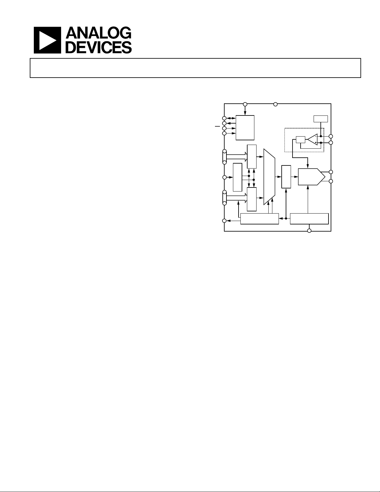
LVDS DDR
RECEIVER
DCI
SDO
SDIO
SCLK
CS
DACCLK
DCO
DB0[13:0]DB1[13:0]
CLK DISTRIBUTION
(DIV-BY-4)
DATA
CONTROLLER
4-TO-1
DATA ASSEMBL E R
SPI
RESET
DLL
(MU CONTRO LLER)
LVDS DDR
RECEIVER
DATA
LATCH
IOUTN
IOUTP
VREF
I120
IRQ
1.2V
DAC BIAS
AD9737A/AD9739A
TxDAC
CORE
09616-001
C
Data Sheet
FEATURES
Direct RF synthesis at 2.5 GSPS update rate
DC to 1.25 GHz in baseband mode
1.25 GHz to 3.0 GHz in mix-mode
Industry leading single/multicarrier IF or RF synthesis
Dual-port LVDS data interface
Up to 1.25 GSPS operation
Source synchronous DDR clocking
Pin compatible with the AD9739
Programmable output current: 8.7 mA to 31.7 mA
Low power: 1.1 W at 2.5 GSPS
APPLICATIONS
Broadband communications systems
DOCSIS CMTS systems
Military jammers
Instrumentation, automatic test equipment
Radar, avionics
11-/14-Bit, 2.5 GSPS,
FUNCTIONAL BLOCK DIAGRAM
Figure 1.
GENERAL DESCRIPTION
The AD9737A/AD9739A are 11-bit and 14-bit, 2.5 GSPS high
performance RF DACs that are capable of synthesizing wideband
signals from dc up to 3 GHz. The AD9737A/AD9739A are pin
and functionally compatible with the AD9739 with the
exception that the AD9737A/AD9739A do not support
synchronization or RZ mode, and are specified to operate
between 1.6 GSPS and 2.5 GSPS.
By elimination of the synchronization circuitry, some nonideal
artifacts such as images and discrete clock spurs remain stationary
on the AD9737A/AD9739A between power-up cycles, thus
allowing for possible system calibration. AC linearity and noise
performance remain the same between the AD9739 and the
AD9737A/AD9739A.
The inclusion of on-chip controllers simplifies system integration.
A dual-port, source synchronous, LVDS interface simplifies the
digital interface with existing FGPA/ASIC technology. On-chip
controllers are used to manage external and internal clock domain
variations over temperature to ensure reliable data transfer from
the host to the DAC core. A serial peripheral interface (SPI) is
used for device configuration as well as readback of status
registers.
Information furnished by Analog Devices is believed to be accurate and reliable. However, no
responsibility is assumed by Analog Devices for its use, nor for any infringements of patents or other
rights of third parties that may result from its use. Specifications subject to change without notice. No
license is granted by implication or otherwise under any patent or patent rights of Analog Devices.
The AD9737A/AD9739A are manufactured on a 0.18 µm
CMOS process and operate from 1.8 V and 3.3 V supplies.
They are supplied in a 160-ball chip scale ball grid array for
reduced package parasitics.
PRODUCT HIGHLIGHTS
1. Ability to synthesize high quality wideband signals with
bandwidths of up to 1.25 GHz in the first or second
Nyquist zone.
2. A proprietary quad-switch DAC architecture provides
exceptional ac linearity performance while enabling mixmode operation.
3. A dual-port, double data rate, LVDS interface supports the
maximum conversion rate of 2500 MSPS.
4. On-chip controllers manage external and internal clock
domain skews.
5. Programmable differential current output with an 8.66 mA
to 31.66 mA range.
One Technology Way, P.O. Box 9106, Norwood, MA 02062-9106, U.S.A.
Tel: 781.329.4700 www.analog.com
Page 2

AD9737A/AD9739A Data Sheet
C
TABLE OF CONTENTS
Features .............................................................................................. 1
Applications ....................................................................................... 1
Functional Block Diagram .............................................................. 1
General Description ......................................................................... 1
Product Highlights ........................................................................... 1
Revision History ............................................................................... 3
Specifications ..................................................................................... 4
DC Specifications ......................................................................... 4
LVDS Digital Specifications ........................................................ 5
Serial Port Specifications ............................................................. 6
AC Specifications .......................................................................... 7
Absolute Maximum Ratings ............................................................ 8
Thermal Resistance ...................................................................... 8
ESD Caution .................................................................................. 8
Pin Configurations and Function Descriptions ........................... 9
Typical Performance Characteristics—AD9737A ..................... 14
Static Linearity ............................................................................ 14
AC (Normal Mode) .................................................................... 15
AC (Mix-Mode) .......................................................................... 17
One-Carrier DOCSIS Performance (Normal Mode) ............ 20
Four-Carrier DOCSIS Performance (Normal Mode) ........... 21
Eight-Carrier DOCSIS Performance (Normal Mode) .......... 22
16-Carrier DOCSIS Performance (Normal Mode) ............... 23
32-Carrier DOCSIS Performance (Normal Mode) ............... 24
64- and 128-Carrier DOCSIS Performance (Normal Mode)25
Typical Performance Characteristics—AD9739A ..................... 26
Static Linearity ............................................................................ 26
AC (Normal Mode) .................................................................... 28
AC (Mix-Mode) .......................................................................... 31
One-Carrier DOCSIS Performance (Normal Mode) ............ 33
Four-Carrier DOCSIS Performance (Normal Mode) ........... 34
Eight-Carrier DOCSIS Performance (Normal Mode) .......... 35
16-Carrier DOCSIS Performance (Normal Mode) ............... 36
32-Carrier DOCSIS Performance (Normal Mode) ............... 37
64- and 128-Carrier DOCSIS Performance (Normal Mode)38
Terminology .................................................................................... 39
Serial Port Interface (SPI) Register ............................................... 40
SPI Register Map Description .................................................. 40
SPI Operation ............................................................................. 40
SPI Register Map ............................................................................ 42
SPI Port Configuration and Software Reset ........................... 43
Power-Down LVDS Interface and TxDAC® ........................... 43
Controller Clock Disable ........................................................... 43
Interrupt Request (IRQ) Enable/Status ................................... 44
TxDAC Full-Scale Current Setting (I
TxDAC Quad-Switch Mode of Operation .............................. 44
DCI Phase Alignment Status .................................................... 44
Data Receiver Controller Configuration ................................. 44
Data Receiver Controller_Data Sample Delay Value ............ 45
Data Receiver Controller_DCI Delay Value/Window and
Phase Rotation ............................................................................ 45
Data Receiver Controller_Delay Line Status .......................... 45
Data Receiver Controller Lock/Tracking Status ..................... 45
CLK Input Common Mode ...................................................... 46
Mu Controller Configuration and Status ................................ 46
Part ID ......................................................................................... 47
Theory of Operation ...................................................................... 48
LVDS Data Port Interface .......................................................... 49
Mu Controller ............................................................................. 52
Interrupt Requests ...................................................................... 54
Analog Interface Considerations .................................................. 55
Analog Modes of Operation ..................................................... 55
Clock Input Considerations ...................................................... 56
Voltage Reference ....................................................................... 57
Analog Outputs .......................................................................... 57
Output Stage Configuration ..................................................... 59
Nonideal Spectral Artifacts ....................................................... 60
Lab Evaluation of the AD9737A/AD9739A ........................... 61
Recommended Start-Up Sequence .......................................... 61
Outline Dimensions ....................................................................... 63
Ordering Guide .......................................................................... 63
) and Sleep ........... 44
OUTFS
Rev. | Page 2 of 64
Page 3

Data Sheet AD9737A/AD9739A
REVISION HISTORY
2/12—Rev. B to Rev. C
Changes to Figure 5 ........................................................................... 9
Changes to Table 7 .......................................................................... 11
Changes to Ordering Guide ........................................................... 63
2/12—Rev. A to Rev. B
Added AD9737A ................................................................ Universal
Reorganized Layout ........................................................... Universal
Moved Revision History Section ..................................................... 3
Deleted ±6% from Table Summary Statement; Changes
to Table 1 ............................................................................................ 4
Deleted ±6% from Table Summary Statement, Table 2 ................ 5
Deleted ±6% from Table Summary Statement, Table 3 ................ 6
Changes to AC Specifications Section and Table 4 ....................... 7
Added Figure 5, Renumbered Sequentially ................................... 9
Added Figure 7 and Table 7, Renumbered Sequentially ............ 10
Deleted Figure 24 ............................................................................ 13
Added Typical Performance Characteristics—AD9737A
Section and Figure 9 to Figure 77 ................................................. 14
Deleted Table 9 ................................................................................ 25
Added Static Linearity Section and Figure 78 to Figure 88 ............ 26
Added Figure 106 ............................................................................ 30
Changes to Figure 116, Figure 117, Figure 118, Figure 119,
Figure 120, and Figure 121 ............................................................. 33
Changes to Figure 122, Figure 123, Figure 124, Figure 125,
Figure 126, and Figure 127 ............................................................. 34
Changes to Figure 128, Figure 129, Figure 130, Figure 131,
Figure 132, and Figure 133 ............................................................. 35
Changes to Figure 134, Figure 135, Figure 136, Figure 137,
Figure 138, and Figure 139 ............................................................. 36
Changes to Figure 140, Figure 141, Figure 142, Figure 143,
Figure 144, and Figure 145 ............................................................. 37
Changes to Figure 146, Figure 147, Figure 148, Figure 149,
and Figure 150; Added Figure 151 ................................................ 38
Added Table 10 ................................................................................ 42
Added SPI Port Configuration and Software Reset Section,
Power-Down LVDS Interface and TxDAC Section, Controller
Clock Disable Section, and Table 11 to Table 13 ........................ 43
Added Interrupt Request (IRQ) Enable/Status Section, TxDAC
Full-Scale Current Setting (I
) and Sleep Section, TxDAC
OUTFS
Quad-Switch Mode of Operation Section, DCI Phase
Alignment Status Section, Data Receiver Controller
Configuration Section, and Table 14 to Table 18 ........................ 44
Added Data Receiver Controller_Data Sample Delay Value
Section, Data Receiver Controller_DCI Delay Value/Window
and Phase Rotation Section, Data Receiver Controller_Delay
Line Status Section, Data Receiver Controller Lock/Tracking
Status Section, and Table 19 to Table 22 ...................................... 45
Added CLK Input Common Mode Section, and Mu
Controller Configuration and Status Section, and Table 23
and Table 24 ..................................................................................... 46
Added Part ID Section, and Table 25 ........................................... 47
Changes to LVDS Data Port Interface Section ............................ 49
Changes to Data Receiver Controller Initialization
Description Section ........................................................................ 51
Changes to Mu Controller Section ............................................... 52
Added Figure 167 and Table 27, Changes to Mu Controller
Initialization Description Section ................................................. 53
Changes to Analog Modes of Operation Section, Figure 171,
and Figure 172 ................................................................................. 55
Updated Outline Dimensions ........................................................ 63
Changes to Ordering Guide ........................................................... 63
7/11—Rev. 0 to Rev. A
Changed Maximum Update Rate (DACCLK Input) Parameter
to DAC Clock Rate Parameter in Table 4 ....................................... 6
Added Adjusted DAC Update Rate Parameter and Endnote 1 in
Table 4 ................................................................................................. 6
Updated Outline Dimensions ........................................................ 43
1/11—Revision 0: Initial Version
Rev. C | Page 3 of 64
Page 4

AD9737A/AD9739A Data Sheet
Parameter
Min
Typ
Max
Min
Typ
Max
Unit
Output Compliance Range
−1.0
+1.0
−1.0 +1.0
V
VDD
1.70
1.8
1.90
1.70
1.8
1.90
V
I
158
167 158
167
mA
I
215
215 mA
C
SPECIFICATIONS
DC SPECIFICATIONS
VDDA = VDD33 = 3.3 V, VDDC = VDD = 1.8 V, I
Table 1.
AD9737A AD9739A
RESOLUTION 11 14 Bits
ACCURACY
Integral Nonlinearity (INL) ±0.5 ±2.5 LSB
Differential Nonlinearity (DNL) ±0.5 ±2.0 LSB
ANALOG OUTPUTS
Gain Error (with Internal Reference) 5.5 5.5 %
Full-Scale Output Current 8.66 20.2 31.66 8.66 20.2 31.66 mA
Common-Mode Output Resistance 10 10 MΩ
Differential Output Resistance 70 70 Ω
Output Capacitance 1 1 pF
DAC CLOCK INPUT (DACCLK_P, DACCLK_N)
Differential Peak-to-Peak Voltage 1.2 1.6 2.0 1.2 1.6 2.0 V
Common-Mode Voltage 900 900 mV
Clock Rate 1.6 2.5 1.6 2.5 GHz
TEMPERATURE DRIFT
Gain 60 60 ppm/°C
Reference Voltage 20 20 ppm/°C
REFERENCE
Internal Reference Voltage 1.15 1.2 1.25 1.15 1.2 1.25 V
Output Resistance 5 5 kΩ
ANALOG SUPPLY VOLTAGES
VDDA 3.1 3.3 3.5 3.1 3.3 3.5 V
VDDC 1.70 1.8 1.90 1.70 1.8 1.90 V
DIGITAL SUPPLY VOLTAGES
VDD33 3.10 3.3 3.5 3.10 3.3 3.5 V
OUTFS
= 20 mA.
SUPPLY CURRENTS AND POWER DISSIPATION, 2.0 GSPS
I
37 38 37 38 mA
VDDA
VDDC
I
14.5 16 14.5 16 mA
VDD33
I
173 183 173 183 mA
VDD
Power Dissipation 0.770 0.770 W
Sleep Mode, I
Power-Down Mode (All Power-Down Bits Set in Register 0x01 and
Register 0x02)
I
0.02 0.02 mA
VDDA
I
6 6 mA
VDDC
I
0.6 0.6 mA
VDD33
I
0.1 0.1 mA
VDD
SUPPLY CURRENTS AND POWER DISSIPATION, 2.5 GSPS
I
223 223 mA
VDDC
I
14.5 14.5 mA
VDD33
VDD
Power Dissipation 0.960 0.960 mW
2.5 2.75 2.5 2.75 mA
VDDA
Rev. | Page 4 of 64
Page 5

Data Sheet AD9737A/AD9739A
Receiver Differential Input Impedance, RIN
80 120
Ω
RO Single-Ended Mismatch
10
%
C
LVDS DIGITAL SPECIFICATIONS
VDDA = VDD33 = 3.3 V, VDDC = VDD = 1.8 V, I
1996 reduced range link, unless otherwise noted.
Table 2.
Parameter Min Typ Max Unit
LVDS DATA INPUTS (DB0[13:0], DB1[13:0])1
Input Common-Mode Voltage Range, V
Logic High Differential Input Threshold, V
Logic Low Differential Input Threshold, V
825 1575 mV
COM
175 400 mV
IH_DTH
−175 −400 mV
IL_DTH
Input Capacitance 1.2 pF
LVDS Input Rate 1250 MSPS
LVDS Minimum Data Valid Period (t
) (See Figure 159) 344 ps
MDE
LVDS CLOCK INPUT (DCI)2
Input Common-Mode Voltage Range, V
Logic High Differential Input Threshold, V
Logic Low Differential Input Threshold, V
825 1575 mV
COM
175 400 mV
IH_DTH
−175 −400 mV
IL_DTH
Receiver Differential Input Impedance, RIN 80 120 Ω
Input Capacitance 1.2 pF
Maximum Clock Rate 625 MHz
LVDS CLOCK OUTPUT (DCO)3
Output Voltage High (DCO_P or DCO_N) 1375 mV
Output Voltage Low (DCO_P or DCO_N) 1025 mV
Output Differential Voltage, |VOD| 150 200 250 mV
Output Offset Voltage, VOS 1150 1250 mV
Output Impedance, Single-Ended, RO 80 100 120 Ω
= 20 mA. LVDS drivers and receivers are compliant to the IEEE Standard 1596.3-
OUTFS
Maximum Clock Rate 625 MHz
1
DB0[x]P, DB0[x]N, DB1[x]P, and DB1[x]N pins.
2
DCI_P and DCI_N pins.
3
DCO_P and DCO_N pins with 100 Ω differential termination.
Rev. | Page 5 of 64
Page 6

AD9737A/AD9739A Data Sheet
SCLK to SDIO Hold Time, tDH
1
ns
READ OPERATION (See Figure 155 and Figure 156)
Current Out High, IOH
4
mA
C
SERIAL PORT SPECIFICATIONS
VDDA = VDD33 = 3.3 V, VDDC = VDD = 1.8 V.
.
Tabl e 3
Parameter Min Typ Max Unit
WRITE OPERATION (See Figure 154)
SCLK Clock Rate, f
SCLK Clock High, t
SCLK Clock Low, t
SDIO to SCLK Setup Time, tDS 2 ns
, 1/t
SCLK
HIGH
LOW
20 MHz
SCLK
18 ns
18 ns
CS to SCLK Setup Time, tS
SCLK to CS Hold Time, tH
SCLK Clock Rate, f
SCLK Clock High, t
SCLK Clock Low, t
, 1/t
SCLK
18 ns
HIGH
18 ns
LOW
20 MHz
SCLK
3 ns
2 ns
SDIO to SCLK Setup Time, tDS 2 ns
SCLK to SDIO Hold Time, tDH 1 ns
CS to SCLK Setup Time, tS
3 ns
SCLK to SDIO (or SDO) Data Valid Time, tDV 15 ns
CS to SDIO (or SDO) Output Valid to High-Z, tEZ
INPUTS (SDI, SDIO, SCLK, CS)
2 ns
Voltage in High, VIH 2.0 3.3 V
Voltage in Low, VIL 0 0.8 V
Current in High, IIH −10 +10 µA
Current in Low, IIL −10 +10 µA
OUTPUT (SDIO)
Voltage Out High, VOH 2.4 3.5 V
Voltage Out Low, VOL 0 0.4 V
Current Out Low, IOL 4 mA
Rev. | Page 6 of 64
Page 7

Data Sheet AD9737A/AD9739A
C
AC SPECIFICATIONS
VDDA = VDD33 = 3.3 V, VDDC = VDD = 1.8 V, I
Table 4.
AD9737A AD9739A
Parameter Min Typ Max Min Typ Max Unit
DYNAMIC PERFORMANCE
DAC Clock Rate 1600 2500 1600 2500 MSPS
Adjusted DAC Update Rate1 1600 2500 1600 2500 MSPS
Output Settling Time to 0.1% 13 13 ns
SPURIOUS-FREE DYNAMIC RANGE (SFDR)
f
= 100 MHz 70 70 dBc
OUT
f
= 350 MHz 65 65 dBc
OUT
f
= 550 MHz 58 58 dBc
OUT
f
= 950 MHz 55 55 dBc
OUT
TWO-TONE INTERMODULATION DISTORTION (IMD),
f
= f
+ 1.25 MHz
OUT1
= 100 MHz 94 94 dBc
= 350 MHz 78 78 dBc
= 550 MHz 72 72 dBc
= 950 MHz 68 68 dBc
f
f
f
f
OUT2
OUT
OUT
OUT
OUT
NOISE SPECTRAL DENSITY (NSD), 0 dBFS SINGLE TONE
f
= 100 MHz −162 −167 dBm/Hz
OUT
f
= 350 MHz −162 −166 dBm/Hz
OUT
f
= 550 MHz −161 −164 dBm/Hz
OUT
f
= 850 MHz −161 −163 dBm/Hz
OUT
WCDMA ACLR (SINGLE CARRIER), ADJACENT/ALTERNATE
ADJACENT CHANNEL
f
= 2457.6 MSPS, f
DAC
f
= 2457.6 MSPS, f
DAC
f
= 2457.6 MSPS, f
DAC
f
= 2457.6 MSPS, f
DAC
1
Adjusted DAC updated rate is calculated as f
is 1. Thus, with f
= 2500 MSPS, f
DAC
= 350 MHz 80/81 80/80 dBc
OUT
= 950 MHz 75/75 78/79 dBc
OUT
= 1700 MHz (Mix-Mode) 69/71 74/74 dBc
OUT
= 2100 MHz (Mix-Mode) 66/67 69/72 dBc
OUT
divided by the minimum required interpolation factor. For the AD9737A/AD9739A, the minimum interpolation factor
DAC
, adjusted, = 2500 MSPS.
DAC
= 20 mA, f
OUTFS
= 2400 MSPS, unless otherwise noted.
DAC
Rev. | Page 7 of 64
Page 8
AD9737A/AD9739A Data Sheet
VDD33 to VSS
−0.3 V to +3.6 V
DACCLK_P, DACCLK_N to VSSC
−0.3 V to VDDC + 0.18 V
C
ABSOLUTE MAXIMUM RATINGS
Table 5.
Parameter Rating
VDDA to VSSA −0.3 V to +3.6 V
THERMAL RESISTANCE
θJA is specified for the worst-case conditions, that is, a device
soldered in a circuit board for surface-mount packages.
VDD to VSS −0.3 V to +1.98 V
VDDC to VSSC −0.3 V to +1.98 V
VSSA to VSS −0.3 V to +0.3 V
VSSA to VSSC −0.3 V to +0.3 V
VSS to VSSC −0.3 V to +0.3 V
DCI, DCO to VSS −0.3 V to VDD33 + 0.3 V
LVDS Data Inputs to VSS −0.3 V to VDD33 + 0.3 V
IOUTP, IOUTN to VSSA −1.0 V to VDDA + 0.3 V
I120, VREF to VSSA −0.3 V to VDDA + 0.3 V
IRQ, CS, SCLK, SDO, SDIO, RESET to VSS
Junction Temperature 150°C
Storage Temperature Range −65°C to +150°C
−0.3 V to VDD33 + 0.3 V
Stresses above those listed under Absolute Maximum Ratings
may cause permanent damage to the device. This is a stress
rating only; functional operation of the device at these or any
other conditions above those indicated in the operational
section of this specification is not implied. Exposure to absolute
maximum rating conditions for extended periods may affect
device reliability.
Table 6. Thermal Resistance
Package Type θJA θJC Unit
160-Ball CSP_BGA 31.2 7.0 °C/W1
1
With no airflow movement.
ESD CAUTION
Rev. | Page 8 of 64
Page 9
Data Sheet AD9737A/AD9739A
PIN CONFIGURATIONS AND FUNCTION DESCRIPTIONS
1413121110876321954
1413121110876321954
A
B
C
D
E
F
G
H
J
K
L
M
N
P
VDDA, 3.3V, ANALOG S UPPLY
VSSA, ANALOG SUPPLY GROUND
VSSA SHIELD, ANAL OG SUPPLY GROUND SHIELD
AD9737A/AD9739A
Figure 2. Analog Supply Pins (Top View)
A
B
C
D
E
F
G
H
J
K
L
M
N
P
VDD, 1.8V, DIGITAL SUPPLY
VSS DIGITAL SUPPLY GROUND
VDD33, 3.3V DIGITAL SUPPLY
AD9737A/AD9739A
Figure 3. Digital Supply Pins (Top View)
A
B
C
D
E
F
G
H
J
K
L
M
N
P
VDDC, 1.8V, CLOCK S UP PLY
VSSC, CLOCK SUPPLY GROUND
09616-002
1413121110876321954
DB1[0:10]P
DB0[0:10]P N
DB0[0:10]N P
Figure 4. Digital LVDS Clock Supply Pins (Top View)
A
B
CDACCLK_N
DDACCLK_P
E
F
G
H
J
K
L
MDB1[0:10]N
DIFFERE NTIAL I NP UT SIGNAL (CLOCK OR DATA)
AD9737A/AD9739A
AD9737A
1413121110876321954
09616-004
DCO_P/_N
DCI_P/_N
09616-036
Figure 5. AD9737A Digital LVDS Input, Clock I/O (Top View)
1413121110876321954
09616-003
DACCLK_N
DACCLK_P
DB1[0:13]P
DB1[0:13]N
DB0[0:13]P
DB0[0:13]N
A
B
C
D
E
F
G
H
J
K
L
M
N
P
AD9739A
DCO_P/_N
DCI_P/_N
Rev. C | Page 9 of 64
DIFFERENTIAL INPUT SIGNAL (CLOCK OR DATA)
Figure 6. AD9739A Digital LVDS Input, Clock I/O (Top View)
09616-005
Page 10
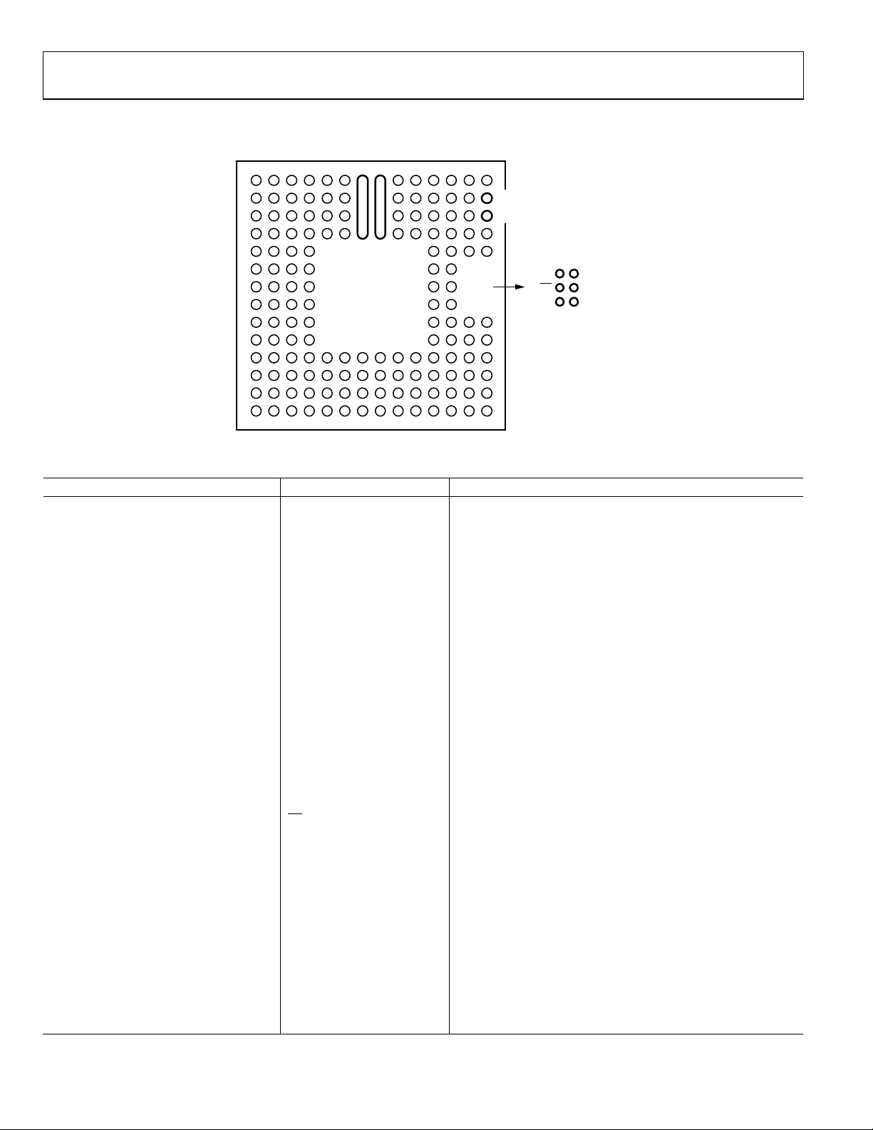
AD9737A/AD9739A Data Sheet
A
B
C
D
E
F
G
H
J
K
L
M
N
P
14131211106321 954
IRQ
CS
SCLK
RESET
SDIO
SDO
7
IOUTN
8
IOUTP
I120
VREF
09616-006
AD9737A
A10, A11, B10, B11, C10, C11, D10, D11
VDDA
3.3 V Analog Supply Input.
A8, B8, C8, D8
IOUTP
DAC Positive Current Output Source.
D14
NC
Factory Test Pin. Do not connect to this pin.
G14
SDIO
Serial Port Data Input/Output.
K13, K14
DCI_P/DCI_N
Positive/Negative Data Clock Input (DCI).
C
Table 7. AD9737A Pin Function Descriptions
Pin No. Mnemonic Description
C1, C2, D1, D2, E1, E2, E3, E4 VDDC 1.8 V Clock Supply Input.
A1, A2, A3, A4, A5, B1, B2, B3, B4, B5, C4,
C5, D4, D5
A12, A13, B12, B13, C12, C13, D12, D13, VSSA Analog Supply Ground.
A6, A9, B6, B9, C6, C9, D6, D9, E11, E12,
E13, E14, F1, F2, F3, F4, F11, F12
A14 NC Do not connect to this pin.
A7, B7, C7, D7 IOUTN DAC Negative Current Output Source.
B14 I120
C14 VREF
C3, D3 DACCLK_N/DACCLK_P Negative/Positive DAC Clock Input (DACCLK).
F13 IRQ
F14 RESET Reset Input. Active high. Tie to VSS if unused.
G13
H13 SCLK Serial Port Clock Input.
H14 SDO Serial Port Data Output.
J3, J4, J11, J12 VDD33 3.3 V Digital Supply Input.
G1, G2, G3, G4, G11, G12 VDD 1.8 V Digital Supply Input.
H1, H2, H3, H4, H11, H12, K3, K4, K11, K12 VSS Digital Supply Ground.
J1, J2 NC
K1, K2 NC
J13, J14 DCO_P/DCO_N Positive/Negative Data Clock Output (DCO).
Figure 7. AD9737A Analog I/O and SPI Control Pins (Top View)
VSSC Clock Supply Ground.
VSSA Shield Analog Supply Ground Shield. Tie to VSSA at the DAC.
Nominal 1.2 V Reference. Tie to analog ground via a 10 kΩ
resistor to generate a 120 µA reference current.
Voltage Reference Input/Output. Decouple to VSSA with a 1 nF
capacitor.
Interrupt Request Open Drain Output. Active high. Pull up to
VDD33 with a 10 kΩ resistor.
CS
Serial Port Enable Input.
Differential resistor of 200 Ω exists between J1 and J2. Do not
Rev. | Page 10 of 64
connect to this pin.
Differential resistor of 100 Ω exists between K1 and K2. Do not
connect to this pin.
Page 11

Data Sheet AD9737A/AD9739A
Pin No. Mnemonic Description
L1, M1 NC, NC Do not connect to this pin.
L2, M2 NC, NC Do not connect to this pin.
L3, M3 NC, NC Do not connect to this pin.
L4, M4 DB1[0]P/DB1[0]N Port 1 Positive/Negative Data Input Bit 0.
L5, M5 DB1[1]P/DB1[1]N Port 1 Positive/Negative Data Input Bit 1.
L6, M6 DB1[2]P/DB1[2]N Port 1 Positive/Negative Data Input Bit 2.
L7, M7 DB1[3]P/DB1[3]N Port 1 Positive/Negative Data Input Bit 3.
L8, M8 DB1[4]P/DB1[4]N Port 1 Positive/Negative Data Input Bit 4.
L9, M9 DB1[5]P/DB1[5]N Port 1 Positive/Negative Data Input Bit 5.
L10, M10 DB1[6]P/DB1[6]N Port 1 Positive/Negative Data Input Bit 6.
L11, M11 DB1[7]P/DB1[7]N Port 1 Positive/Negative Data Input Bit 7.
L12, M12 DB1[8]P/DB1[8]N Port 1 Positive/Negative Data Input Bit 8.
L13, M13 DB1[9]P/DB1[9]N Port 1 Positive/Negative Data Input Bit 9.
L14, M14 DB1[10]P/DB1[10]N Port 1 Positive/Negative Data Input Bit 10.
N1, P1 NC, NC Do not connect to this pin.
N2, P2 NC, NC Do not connect to this pin.
N3, P3 NC, NC Do not connect to this pin.
N4, P4 DB0[0]P/DB0[0]N Port 0 Positive/Negative Data Input Bit 0.
N5, P5 DB0[1]P/DB0[1]N Port 0 Positive/Negative Data Input Bit 1.
N6, P6 DB0[2]P/DB0[2]N Port 0 Positive/Negative Data Input Bit 2.
N7, P7 DB0[3]P/DB0[3]N Port 0 Positive/Negative Data Input Bit 3.
N8, P8 DB0[4]P/DB0[4]N Port 0 Positive/Negative Data Input Bit 4.
N9, P9 DB0[5]P/DB0[5]N Port 0 Positive/Negative Data Input Bit 5.
N10, P10 DB0[6]P/DB0[6]N Port 0 Positive/Negative Data Input Bit 6.
N11, P11 DB0[7]P/DB0[7]N Port 0 Positive/Negative Data Input Bit 7.
N12, P12 DB0[8]P/DB0[8]N Port 0 Positive/Negative Data Input Bit 8.
N13, P13 DB0[9]P/DB0[9]N Port 0 Positive/Negative Data Input Bit 9.
N14, P14 DB0[10]P/DB0[10]N Port 0 Positive/Negative Data Input Bit 10.
Rev. C | Page 11 of 64
Page 12

AD9737A/AD9739A Data Sheet
IOUTN8IOUTP
7
A
B
C
D
E
F
G
H
J
K
L
M
N
P
Figure 8. AD9739A Analog I/O and SPI Control Pins (Top View)
AD9739A
14131211106321954
I120
VREF
IRQ
CS
SCLK
RESET
SDIO
SDO
09616-037
Table 8. AD9739A Pin Function Descriptions
Pin No. Mnemonic Description
C1, C2, D1, D2, E1, E2, E3, E4 VDDC 1.8 V Clock Supply Input.
A1, A2, A3, A4, A5, B1, B2, B3, B4, B5, C4,
VSSC Clock Supply Ground.
C5, D4, D5
A10, A11, B10, B11, C10, C11, D10, D11 VDDA 3.3 V Analog Supply Input.
A12, A13, B12, B13, C12, C13, D12, D13, VSSA Analog Supply Ground.
A6, A9, B6, B9, C6, C9, D6, D9, E11, E12,
VSSA Shield Analog Supply Ground Shield. Tie to VSSA at the DAC.
E13, E14, F1, F2, F3, F4, F11, F12
A14 NC Do not connect to this pin.
A7, B7, C7, D7 IOUTN DAC Negative Current Output Source.
A8, B8, C8, D8 IOUTP DAC Positive Current Output Source.
B14 I120
Nominal 1.2 V Reference. Tie to analog ground via a 10 kΩ
resistor to generate a 120 μA reference current.
C14 VREF
Voltage Reference Input/Output. Decouple to VSSA with a 1 nF
capacitor.
D14 NC Factory Test Pin. Do not connect to this pin.
C3, D3 DACCLK_N/DACCLK_P Negative/Positive DAC Clock Input (DACCLK).
F13 IRQ
Interrupt Request Open Drain Output. Active high. Pull up to
VDD33 with a 10 kΩ resistor.
F14 RESET Reset Input. Active high. Tie to VSS if unused.
G13
CS
Serial Port Enable Input.
G14 SDIO Serial Port Data Input/Output.
H13 SCLK Serial Port Clock Input.
H14 SDO Serial Port Data Output.
J3, J4, J11, J12 VDD33 3.3 V Digital Supply Input.
G1, G2, G3, G4, G11, G12 VDD 1.8 V Digital Supply Input.
H1, H2, H3, H4, H11, H12, K3, K4, K11, K12 VSS Digital Supply Ground.
J1, J2 NC
Differential resistor of 200 Ω exists between J1 and J2. Do not
connect to this pin.
K1, K2 NC
Differential resistor of 100 Ω exists between K1 and K2. Do not
connect to this pin.
J13, J14 DCO_P/DCO_N Positive/Negative Data Clock Output (DCO).
K13, K14 DCI_P/DCI_N Positive/Negative Data Clock Input (DCI).
Rev. C | Page 12 of 64
Page 13

Data Sheet AD9737A/AD9739A
Pin No. Mnemonic Description
L1, M1 DB1[0]P/DB1[0]N Port 1 Positive/Negative Data Input Bit 0.
L2, M2 DB1[1]P/DB1[1]N Port 1 Positive/Negative Data Input Bit 1.
L3, M3 DB1[2]P/DB1[2]N Port 1 Positive/Negative Data Input Bit 2.
L4, M4 DB1[3]P/DB1[3]N Port 1 Positive/Negative Data Input Bit 3.
L5, M5 DB1[4]P/DB1[4]N Port 1 Positive/Negative Data Input Bit 4.
L6, M6 DB1[5]P/DB1[5]N Port 1 Positive/Negative Data Input Bit 5.
L7, M7 DB1[6]P/DB1[6]N Port 1 Positive/Negative Data Input Bit 6.
L8, M8 DB1[7]P/DB1[7]N Port 1 Positive/Negative Data Input Bit 7.
L9, M9 DB1[8]P/DB1[8]N Port 1 Positive/Negative Data Input Bit 8.
L10, M10 DB1[9]P/DB1[9]N Port 1 Positive/Negative Data Input Bit 9.
L11, M11 DB1[10]P/DB1[10]N Port 1 Positive/Negative Data Input Bit 10.
L12, M12 DB1[11]P/DB1[11]N Port 1 Positive/Negative Data Input Bit 11.
L13, M13 DB1[12]P/DB1[12]N Port 1 Positive/Negative Data Input Bit 12.
L14, M14 DB1[13]P/DB1[13]N Port 1 Positive/Negative Data Input Bit 13.
N1, P1 DB0[0]P/DB0[0]N Port 0 Positive/Negative Data Input Bit 0.
N2, P2 DB0[1]P/DB0[1]N Port 0 Positive/Negative Data Input Bit 1.
N3, P3 DB0[2]P/DB0[2]N Port 0 Positive/Negative Data Input Bit 2.
N4, P4 DB0[3]P/DB0[3]N Port 0 Positive/Negative Data Input Bit 3.
N5, P5 DB0[4]P/DB0[4]N Port 0 Positive/Negative Data Input Bit 4.
N6, P6 DB0[5]P/DB0[5]N Port 0 Positive/Negative Data Input Bit 5.
N7, P7 DB0[6]P/DB0[6]N Port 0 Positive/Negative Data Input Bit 6.
N8, P8 DB0[7]P/DB0[7]N Port 0 Positive/Negative Data Input Bit 7.
N9, P9 DB0[8]P/DB0[8]N Port 0 Positive/Negative Data Input Bit 8.
N10, P10 DB0[9]P/DB0[9]N Port 0 Positive/Negative Data Input Bit 9.
N11, P11 DB0[10]P/DB0[10]N Port 0 Positive/Negative Data Input Bit 10.
N12, P12 DB0[11]P/DB0[11]N Port 0 Positive/Negative Data Input Bit 11.
N13, P13 DB0[12]P/DB0[12]N Port 0 Positive/Negative Data Input Bit 12.
N14, P14 DB0[13]P/DB0[13]N Port 0 Positive/Negative Data Input Bit 13.
Rev. C | Page 13 of 64
Page 14
AD9737A/AD9739A Data Sheet
0.3
–0.4
0 2048
ERROR (LSB)
CODE
–0.3
–0.2
–0.1
0
0.1
0.2
256 512 768 1024 1280 1536 1792
09616-109
0.4
–0.3
0 2048
ERROR (LSB)
CODE
–0.2
–0.1
0
0.1
0.2
0.3
256 512 768 1024 1280 1536 1792
09616-110
0.25
–0.25
0 2048
ERROR (LSB)
CODE
–0.20
–0.10
–0.15
–0.05
0
0.10
0.05
0.15
0.20
256 512 768 1024 1280 1536 1792
09616-111
0.25
–0.25
0 2048
ERROR (LSB)
CODE
–0.20
–0.10
–0.15
–0.05
0
0.10
0.05
0.15
0.20
256 512 768 1024 1280 1536 1792
09616-112
0.6
–0.6
–0.5
–0.4
–0.3
0 2048
ERROR (LSB)
CODE
–0.2
–0.1
0
0.1
0.2
0.3
0.5
0.4
256 512 768 1024 1280 1536 1792
09616-113
0.2
–0.8
–0.7
–0.6
–0.5
–0.4
–0.3
0 2048
ERROR (LSB)
CODE
–0.2
–0.1
0
0.1
256 512 768 1024 1280 1536 1792
09616-114
C
TYPICAL PERFORMANCE CHARACTERISTICS—AD9737A
STATIC LINEARITY
I
= 20 mA, nominal supplies, TA = 25°C, unless otherwise noted.
OUTFS
Figure 9. Typical INL, 20 mA at 25°C
Figure 10. Typical DNL, 20 mA at 25°C
Figure 12. Typical DNL, 10 mA at 25°C
Figure 13. Typical INL, 30 mA at 25°C
Figure 11. Typical INL, 10 mA at 25°C
Figure 14. Typical DNL, 30 mA at 25°C
Rev. | Page 14 of 64
Page 15
Data Sheet AD9737A/AD9739A
10dB/DIV
STOP 2.4GHzSTART 20MHz
VBW 20kHz
09616-115
10dB/DIV
VBW 20kHz
STOP 2.4GHzSTART 20MHz
09616-116
90
80
0
10
20
30
40
50
60
70
0 12001000800600400200
SFDR (dBc)
f
OUT
(MHz)
1.6GSPS
2.4GSPS
1.2GSPS
2.0GSPS
09616-117
120
100
80
60
40
20
0
0 200 400 600 800 1000 1200 1400
IIMD (d Bc)
f
OUT
(MHz)
2.0GSPS
1.6GSPS
1.2GSPS
2.4GSPS
09616-118
–150
–170
0 200 400 600 800 1000 1200
NSD (dBm/Hz)
f
OUT
(MHz)
1.2GSPS
2.4GSPS
–168
–166
–164
–162
–160
–158
–156
–154
–152
09616-119
–150
–170
0 200 400 600 800 1000 1200
NSD (dBm/Hz)
f
OUT
(MHz)
1.2GSPS
2.4GSPS
–168
–166
–164
–162
–160
–158
–156
–154
–152
09616-120
C
AC (NORMAL MODE)
I
= 20 mA, nominal supplies, TA = 25°C, unless otherwise noted.
OUTFS
Figure 15. Single Tone Spectrum at f
Figure 16. Single-Tone Spectrum at f
= 91 MHz, f
OUT
= 1091 MHz, f
OUT
= 2.4 GSPS
DAC
= 2.4 GSPS
DAC
Figure 18. IMD vs. f
OUT
over f
DAC
Figure 19. Single-Tone NSD over f
OUT
Figure 17. SFDR vs. f
OUT
over f
DAC
Figure 20. Eight-Tone NSD over f
OUT
Rev. | Page 15 of 64
Page 16
AD9737A/AD9739A Data Sheet
90
30
0 200 300100 400 600 700500 900800 1000
SFDR (dBc)
f
OUT
(MHz)
35
40
45
50
55
60
65
70
75
80
85
–3dBFS
0dBFS
–6dBFS
09616-121
90
30
0 200 400 600 800 1000
SFDR (dBc)
f
OUT
(MHz)
40
50
60
70
80
–3dBFS
0dBFS
–6dBFS
09616-122
90
30
0 200 400 600 800 1000
SFDR (dBc)
f
OUT
(MHz)
40
50
60
70
80
0dBFS
–6dBFS
–3dBFS
09616-123
100
40
0 1000
IMD (dBc)
f
OUT
(MHz)
0dBFS
45
50
55
60
65
70
75
80
85
90
95
100 200 300 400 500 600 700 800 900
–3dBFS
–6dBFS
09616-124
30
40
35
0 1000
SFDR (dBc)
f
OUT
(MHz)
45
50
55
60
65
70
75
80
85
90
100 200 300 400 500 600 700 800 900
30mA FS
10mA FS
20mA FS
09616-125
40
0 1000
IMD (dBc)
f
OUT
(MHz)
45
50
55
60
65
70
75
80
85
90
95
100
100 200 300 400 500 600 700 800 900
20mA FS
30mA FS
10mA FS
09616-126
C
f
= 2 GSPS, I
DAC
= 20 mA, nominal supplies, TA = 25°C, unless otherwise noted.
OUTFS
Figure 21. SFDR vs. f
over Digital Full Scale
OUT
Figure 22. SFDR for Second Harmonic vs. f
over Digital Full Scale
OUT
Figure 24. IMD vs. f
Figure 25. SFDR vs. f
over Digital Full Scale
OUT
over DAC I
OUT
OUTFS
Figure 23. SFDR for Third Harmonic vs. f
over Digital Full Scale
OUT
Rev. | Page 16 of 64
Figure 26. IMD vs. f
over DAC I
OUT
OUTFS
Page 17
Data Sheet AD9737A/AD9739A
09616-127
30
40
35
0 1000
SFDR (dBc)
f
OUT
(MHz)
45
50
55
60
65
70
75
80
85
90
100 200 300 400 500 600 700 800 900
+85°C
–40°C
+25°C
09616-128
40
0 1000
IMD (dBc)
f
OUT
(MHz)
45
50
55
60
65
70
75
80
85
90
95
100
100 200 300 400 500 600 700 800 900
–40°C
+25°C
+85°C
09616-129
–170
–168
–166
–164
–162
–160
–158
–156
–154
–152
–150
0 200 400 600 800 1000100 300 500 700 900
f
OUT
(MHz)
NSD (dBm/Hz)
+25°C
+85°C
09616-130
–170
–168
–166
–164
–162
–160
–158
–156
–154
–152
–150
0 200 400 600 800 1000100 300 500 700 900
f
OUT
(MHz)
NSD (dBm/Hz)
+25°C
+85°C
SPAN 54.68MHz
SWEEP 1.509s
CENTER 350MHz
#RES BW 30kHz
UPPER
FILTER
ON
ON
ON
ON
ON
dBc
–79.73
–80.21
–80.85
–81.41
–81.46
dBc
–80.51
–81.11
–81.67
–81.61
–82.19
dBm
–92.90
–93.38
–94.01
–94.58
–94.63
LOWER
dBm
–93.67
–94.27
–94.84
–94.77
–95.35
INTEG B W
3.840MHz
3.840MHz
3.840MHz
3.840MHz
3.840MHz
OFFSET FREQ
5.000MHz
10.00MHz
15.00MHz
20.00MHz
25.00MHz
CARRIER POWER –13.167dBm/3.84MHz ACP-IBW
10dB/DIV
–35
–45
–55
–65
–75
–85
–95
–105
–115
09616-131
VBW 3kHz
–81.4dBc–81.1dBc
–80.5dBc –13.2dBm
–80.8dBc
–80.2dBc
–79.7dBc –81.5dBc
–81.6dBc–82.2dBc
–81.7dBc
–50
–55
–60
–65
–70
–75
–80
–85
–90
0 200 400 600 800 140012001000
ACLR (dBc)
f
OUT
(MHz)
09616-226
FIRST ADJ CH
FIFT H ADJ CH
SECOND ADJ CH
C
AC (MIX-MODE)
f
= 2.1 GSPS, I
DAC
= 20 mA, nominal supplies, TA = 25°C, unless otherwise noted.
OUTFS
Figure 27. SFDR vs. f
over Temperature
OUT
Figure 30. Eight-Tone NSD vs. f
over Temperature
OUT
Figure 28. IMD vs. f
Figure 29. Single-Tone NSD vs. f
over Temperature
OUT
over Temperature
OUT
Figure 31. Single-Carrier WCDMA at 350 MHz, f
Figure 32. Single-Carrier WCDMA ACLR vs. f
= 2457.6 MSPS
DAC
at 2457.6 MSPS
OUT
Rev. | Page 17 of 64
Page 18
AD9737A/AD9739A Data Sheet
09616-132
10dB/DIV
STOP 2.4GHz
SWEEP 7.174s (601pts)
START 20MHz
#RES BW 20kHz
VBW 20kHz
09616-133
10dB/DIV
STOP 2.4GHz
SWEEP 7.174s (601pts)
START 20MHz
#RES BW 20kHz
VBW 20kHz
09616-134
10
15
20
25
30
35
40
45
50
55
60
65
70
75
80
1200 1300 1400 1500 1600 1700 1800 1900 2000 2100 2200 2300 2400
f
OUT
(MHz)
SFDR (dBc)
09616-135
30
40
50
60
70
90
80
100
1000 130012001100 1400 1500 1600 1700 1800 1900 2000
IMD (dBc)
f
OUT
(MHz)
09616-136
SPAN 54.68MHz
SWEEP 1.509s
CENTER 2.108MHz
#RES BW 30kHz
UPPER
FILTER
ON
ON
ON
ON
ON
dBc
–69.84
–71.15
–71.75
–72.19
–72.70
dBc
–69.82
–69.93
–71.77
–72.26
–71.90
dBm
–89.36
–90.67
–91.28
–91.71
–92.22
LOWER
dBm
–88.34
–89.46
–91.29
–91.79
–91.42
INTEG B W
3.840MHz
3.840MHz
3.840MHz
3.840MHz
3.840MHz
OFFSET FREQ
5.000MHz
10.00MHz
15.00MHz
20.00MHz
25.00MHz
CARRIER POWER –19.526dBm/3.84MHz ACP-IBW
10dB/DIV
–35
–45
–55
–65
–75
–85
–95
–105
–115
VBW 3kHz
–72.7dBc
–71.8dBc –69.9dBc –68.8dBc
–19.5dBm
–72.3dBc–71.9dBc –69.8dBc –71.1dBc –71.8dBc –72.2dBc
f
DAC
= 2457.6 MSPS (Second Nyquist Zone)
–90
–85
–80
–75
–70
–65
–60
–55
–50
1307.6
3557.6
1557.6
1807.6
2057.6
2307.6
2557.6
2807.6
3057.6
3307.6
SECOND NYQUI S T ZONE THIRD NYQUIST ZONE
FIRST ADJ CH
THIRD ADJ CH
ACLR (dBc)
09616-137
f
OUT
(MHz)
SECOND ADJ CH
Figure 38. Single-Carrier WCDMA ACLR vs. f
OUT
, f
DAC
= 2457.6 MSPS
C
f
= 2.1 GSPS, I
DAC
= 20 mA, nominal supplies, TA = 25°C, unless otherwise noted.
OUTFS
Figure 33. Single-Tone Spectrum at f
Figure 34. Single-Tone Spectrum at f
= 2.31 GHz, f
OUT
= 1.31 GHz, f
OUT
= 2.4 GSPS
DAC
= 2.4 GSPS
DAC
Figure 36. IMD in Mix-Mode vs. f
at 2.4 GSPS
OUT
Figure 37. Typical Single-Carrier WCDMA ACLR Performance at 2.1 GHz,
Figure 35. SFDR in Mix-mode vs. f
at 2.4 GSPS
OUT
Rev. | Page 18 of 64
Page 19
Data Sheet AD9737A/AD9739A
09616-138
SPAN 54.68MHz
SWEEP 1.509s
CENTER 2.808MHz
#RES BW 30kHz
UPPER
FILTER
ON
ON
ON
ON
ON
dBc
–65.56
–65.82
–65.98
–66.06
–66.14
dBc
–65.65
–65.70
–65.81
–65.84
–65.84
dBm
–94.72
–94.98
–95.14
–95.22
–95.31
LOWER
dBm
–94.81
–94.86
–94.97
–95.00
–95.00
INTEG B W
3.840MHz
3.840MHz
3.840MHz
3.840MHz
3.840MHz
OFFSET FREQ
5.000MHz
10.00MHz
15.00MHz
20.00MHz
25.00MHz
CARRIER POWER –26.161dBm/3.84MHz ACP-IBW
10dB/DIV
–45
–55
–65
–75
–85
–95
–115
–105
–125
VBW 3kHz
–66.1dBc –66.1dBc–65.8dBc –65.7dBc
–65.6dBc –29.2dBm–65.8dBc –65.8dBc –65.6dBc –65.8dBc –66.0dBc
09616-139
SPAN 69.68MHz
SWEEP 1.922s
CENTER 2.108MHz
#RES BW 30kHz
UPPER
FILTER
ON
ON
ON
ON
ON
dBc
–64.93
–64.26
–65.21
–65.74
–66.13
dBc
–65.42
–64.93
–65.12
–65.24
–65.61
dBm
–92.23
–91.56
–92.50
–93.04
–93.42
LOWER
dBm
–92.72
–92.23
–92.42
–92.53
–92.91
INTEG B W
3.840MHz
3.840MHz
3.840MHz
3.840MHz
3.840MHz
OFFSET FREQ
5.000MHz
10.00MHz
15.00MHz
20.00MHz
25.00MHz
CARRIER POWER –21.446dBm/15.36MHz ACP-IBW
10dB/DIV
–50
–60
–70
–80
–90
–100
–120
–110
–130
VBW 3kHz
–65.2dBc
–65.4dBc
–27.6dBm
–27.6dBm
–27.3dBm
–27.4dBm
–64.9dBc–64.9dBc
–64.3dBc –65.7dBc
–66.1dBc
–65.1dBc
–65.2dBc
–65.6dBc
09616-140
SPAN 69.68MHz
SWEEP 1.922s
CENTER 2.808MHz
#RES BW 30kHz
UPPER
FILTER
ON
ON
ON
ON
ON
dBc
–58.20
–58.15
–58.26
–58.33
–58.21
dBc
–58.05
–57.95
–57.95
–57.97
–58.05
dBm
–95.26
–95.21
–95.32
–95.39
–95.27
LOWER
dBm
–95.11
–95.02
–95.01
–95.04
–95.11
INTEG B W
3.840MHz
3.840MHz
3.840MHz
3.840MHz
3.840MHz
OFFSET FREQ
5.000MHz
10.00MHz
15.00MHz
20.00MHz
25.00MHz
CARRIER POWER –31.097dBm/15.36MHz ACP-IBW
10dB/DIV
–60
–70
–80
–90
–100
–110
–130
–120
–140
VBW 3kHz
–58.3dBc
–58.0dBc
–37.4dBm
–37.1dBm
–37.1dBm
–36.9dBm
–58.2dBc–58.0dBc
–58.1dBc –58.3dBc
–58.2dBc
–57.9dBc
–58.0dBc
–58.0dBc
C
f
= 2.1 GSPS, I
DAC
= 20 mA, nominal supplies, TA = 25°C, unless otherwise noted.
OUTFS
Figure 39. Typical Single-Carrier WCDMA ACLR Performance at 2.8 GHz,
f
= 2457.6 MSPS (Third Nyquist Zone)
DAC
Figure 40. Typical Four-Carrier WCDMA ACLR Performance at 2.1 GHz,
f
= 2457.6 MSPS (Second Nyquist Zone)
DAC
Figure 41. Typical Four-Carrier WCDMA ACLR Performance at 2.8 GHz,
= 2457.6 MSPS (Third Nyquist Zone)
f
DAC
Rev. | Page 19 of 64
Page 20
AD9737A/AD9739A Data Sheet
09616-141
10dB/DIV
VBW 2kHz
STOP 1GHz
SWEEP 24.1s (1001pts)
START 50MHz
#RES BW 20kHz
FUNCTION
VALUE
FUNCTION
WIDTHFUNCTION
–10.238dBm
–74.467dB
–77.224dB
–78.437dB
–67.413dB
6MHz
6MHz
6MHz
6MHz
6MHz
BAND POWER
BAND POWER
BAND POWER
BAND POWER
BAND POWER
(Δ)
(Δ)
(Δ)
(Δ)
(Δ)
(Δ)
(Δ)
(Δ)
(Δ)
(Δ)
(Δ)
(Δ)
Y
–10.238dBm
–74.467dB
–77.224dB
–78.437dB
–67.413dB
f
f
f
f
f
1
1
1
1
1
1
2
3
4
5
X
N
Δ1
Δ1
Δ1
Δ1
MODEMKR SCLTRC
200.10MHz
199.50MHz
399.95MHz
599.45MHz
413.25MHz
–30
–40
–50
–60
–70
–80
–90
–100
–110
4Δ1
1
2Δ1
3Δ1
5Δ1
Figure 42. Low Band Wideband ACLR
09616-142
10dB/DIV
VBW 2kHz
STOP 1GHz
SWEEP 24.1s (1001pts)
START 50MHz
#RES BW 20kHz
FUNCTION
VALUE
FUNCTION
WIDTHFUNCTION
–11.538dBm
–74.399dB
–74.344dB
–68.472dB
–66.197dB
6MHz
6MHz
6MHz
6MHz
6MHz
BAND POWER
BAND POWER
BAND POWER
BAND POWER
BAND POWER
(Δ)
(Δ)
(Δ)
(Δ)
(Δ)
(Δ)
(Δ)
(Δ)
(Δ)
(Δ)
(Δ)
(Δ)
Y
–11.538dBm
–74.421dB
–76.294dB
–68.472dB
–66.156dB
f
f
f
f
f
1
1
1
1
1
1
2
3
4
5
X
N
Δ1
Δ1
Δ1
Δ1
MODEMKR SCLTRC
550.65MHz
–487.35MHz
125.40MHz
253.65MHz
62.70MHz
–30
–40
–50
–60
–70
–80
–90
–100
–110
3Δ1
2Δ1
1
4Δ1
5Δ1
Figure 43. Mid Band Wideband ACLR
09616-143
10dB/DIV
VBW 2kHz
STOP 1GHz
SWEEP 24.1s (1001pts)
START
50MHz
#RES BW 20kHz
FUNCTION
VALUE
FUNCTION
WIDTHFUNCTION
–14.446dBm
–60.856dB
–66.013dB
–68.697dB
–63.533dB
–68.162dB
6MHz
6MHz
6MHz
6MHz
6MHz
6MHz
BAND POWER
BAND POWER
BAND POWER
BAND POWER
BAND POWER
BAND POWER
(Δ)
(Δ)
(Δ)
(Δ)
(Δ)
(Δ)
(Δ)
(Δ)
(Δ)
(Δ)
(Δ)
(Δ)
(Δ)
(Δ)
(Δ)
Y
–14.418dBm
–60.856dB
–66.000dB
–68.751dB
–63.533dB
–66.162dB
f
f
f
f
f
f
1
1
1
1
1
1
1
2
3
4
5
6
X
N
Δ1
Δ1
Δ1
Δ1
Δ1
MODEMKR SCLTRC
948.70MHz
–393.30MHz
–553.85MHz
–612.75MHz
–335.35MHz
–57.95MHz
–30
–40
–50
–60
–70
–80
–90
–100
–110
3Δ1
5Δ1
4Δ1
2Δ1
6Δ1
1
Figure 44. High Band Wideband ACLR
09616-144
SPAN 54MHz
SWEEP 1.49s
VBW 3kHz
CENTER 200MHz
#RES BW 30kHz
UPPER
FILTER
OFF
OFF
OFF
OFF
OFF
dBc
–57.47
–79.87
–78.96
–78.69
–78.68
dBc
–58.34
–79.27
–78.44
–78.59
–78.41
dBm
–67.70
–90.10
–89.19
–88.92
–88.90
LOWER
dBm
–68.57
–89.50
–88.66
–88.82
–88.63
INTEG B W
750.0kHz
5.250MHz
6.000MHz
6.000MHz
6.000MHz
OFFSET FREQ
3.375MHz
6.375MHz
12.00MHz
18.00MHz
24.00MHz
CARRIER POWER – 1 0 .226dBm/6MHz ACP-IBW
10dB/DIV
–30
–40
–50
–60
–70
–80
–90
–100
–110
–78.4dBc
–78.6dBc –78.4dBc
–79.3dBc –10.2dBm
–79.9dBc –79.0dBc
–78.7dBc–78.7dBc
Figure 45. Low Band Narrow-Band ACLR
09616-145
SPAN 54MHz
SWEEP 1.49s
VBW 3kHz
CENTER 550MHz
#RES BW 30kHz
UPPER
FILTER
OFF
OFF
OFF
OFF
OFF
dBc
–60.92
–74.14
–74.68
–74.91
–75.34
dBc
–59.37
–74.02
–74.53
–75.00
–75.97
dBm
–73.03
–86.25
–86.79
–87.01
–87.44
LOWER
dBm
–71.48
–86.12
–86.63
–87.11
–88.08
INTEG B W
750.0kHz
5.250MHz
6.000MHz
6.000MHz
6.000MHz
OFFSET FREQ
3.375MHz
6.375MHz
12.00MHz
18.00MHz
24.00MHz
CARRIER POWER – 1 2 .104dBm/6MHz ACP-IBW
10dB/DIV
–30
–40
–50
–60
–70
–80
–90
–100
–110
–76.0dBc –75.0dBc –74.5dBc –74.0dBc –12.1dBm –74.1dBc –74.7dBc –75.3dBc–78.9dBc
Figure 46. Mid Band Narrow-Band ACLR
09616-146
SPAN 54MHz
SWEEP 1.49s
VBW 3kHz
CENTER 950MHz
#RES BW 30kHz
UPPER
FILTER
OFF
OFF
OFF
OFF
OFF
dBc
–61.30
–69.39
–70.50
–71.02
–71.75
dBc
–57.84
–69.02
–70.01
–70.89
–71.94
dBm
–74.89
–82.98
–84.09
–84.61
–85.34
LOWER
dBm
–71.43
–82.61
–83.60
–84.48
–85.53
INTEG B W
750.0kHz
5.250MHz
6.000MHz
6.000MHz
6.000MHz
OFFSET FREQ
3.375MHz
6.375MHz
12.00MHz
18.00MHz
24.00MHz
CARRIER POWER – 1 3 .589dBm/6MHz ACP-IBW
10dB/DIV
–30
–40
–50
–60
–70
–80
–90
–100
–110
–71.9dBc –70.9dBc –70.0dBc
–69.0dBc –13.6dBm –69.4dBc –70.5dBc –71.7dBc–71.0dBc
Figure 47. High Band Narrow-Band ACLR
C
ONE-CARRIER DOCSIS PERFORMANCE (NORMAL MODE)
I
= 20 mA, f
OUTFS
= 2.4576 GSPS, nominal supplies, TA = 25°C, unless otherwise noted.
DAC
Rev. | Page 20 of 64
Page 21

Data Sheet AD9737A/AD9739A
STOP 1GHz
SWEEP 24.1s (1001pts)
START 50MHz
#RES BW 20kHz
10dB/DIV
–30
–40
–50
–60
–70
–80
–90
–100
–110
09616-147
VBW 2kHz
1
2Δ1
5Δ1
3Δ1
4Δ1
FUNCTION
VALUE
FUNCTION
WIDTHFUNCTION
–18.419dBm
–69.277dB
–71.485dB
–72.343dB
–59.518dB
6MHz
6MHz
6MHz
6MHz
6MHz
BAND POWER
BAND POWER
BAND POWER
BAND POWER
BAND POWER
(Δ)
(Δ)
(Δ)
(Δ)
(Δ)
(Δ)
(Δ)
(Δ)
(Δ)
(Δ)
(Δ)
(Δ)
Y
–18.419dBm
–69.252dB
–71.282dB
–72.100dB
–59.520dB
f
f
f
f
f
1
1
1
1
1
1
2
3
4
5
X
N
Δ1
Δ1
Δ1
Δ1
MODEMKR SCLTRC
200.10MHz
221.35MHz
431.30MHz
651.70MHz
413.25MHz
Figure 48. Low Band Wideband ACLR
STOP 1GHz
SWEEP 24.1s (1001pts)
START 50MHz
#RES BW 20kHz
10dB/DIV
–30
–40
–50
–60
–70
–80
–90
–100
–110
09616-148
VBW 2kHz
1
2Δ1
5Δ1
3Δ1
4Δ1
FUNCTION
VALUE
FUNCTION
WIDTHFUNCTION
–19.885dBm
–70.252dB
–69.581dB
–67.793dB
–58.085dB
6MHz
6MHz
6MHz
6MHz
6MHz
BAND POWER
BAND POWER
BAND POWER
BAND POWER
BAND POWER
(Δ)
(Δ)
(Δ)
(Δ)
(Δ)
(Δ)
(Δ)
(Δ)
(Δ)
(Δ)
(Δ)
(Δ)
Y
–19.885dBm
–70.252dB
–69.535dB
–67.793dB
–58.085dB
f
f
f
f
f
1
1
1
1
1
1
2
3
4
5
X
N
Δ1
Δ1
Δ1
Δ1
MODEMKR SCLTRC
549.70MHz
–486.40MHz
126.35MHz
228.00MHz
63.65MHz
Figure 49. Mid Band Wideband ACLR
STOP 1GHz
SWEEP 24.1s (1001pts)
START 50MHz
#RES BW 20kHz
10dB/DIV
–40
–50
–60
–70
–80
–90
–100
–110
–120
09616-149
VBW 2kHz
1
2Δ1
5Δ1
6Δ1
3Δ1
4Δ1
FUNCTION
VALUE
FUNCTION
WIDTHFUNCTION
–21.676dBm
–62.206dB
–65.730dB
–67.064dB
–56.405dB
–65.729dB
6MHz
6MHz
6MHz
6MHz
6MHz
6MHz
BAND POWER
BAND POWER
BAND POWER
BAND POWER
BAND POWER
BAND POWER
(Δ)
(Δ)
(Δ)
(Δ)
(Δ)
(Δ)
(Δ)
(Δ)
(Δ)
(Δ)
(Δ)
(Δ)
(Δ)
(Δ)
(Δ)
Y
–21.631dBm
–62.206dB
–65.730dB
–67.064dB
–56.405dB
–65.729dB
f
f
f
f
f
f
1
1
1
1
1
1
1
2
3
4
5
6
X
N
Δ1
Δ1
Δ1
Δ1
Δ1
MODEMKR SCLTRC
950.60MHz
–415.15MHz
–529.15MHz
–610.85MHz
–337.25MHz
–59.85MHz
Figure 50. High Band Wideband ACLR
SPAN 54MHz
SWEEP 1.49s
CENTER 218MHz
#RES BW 30kHz
UPPER
FILTER
OFF
OFF
OFF
OFF
OFF
dBc
–58.82
–73.28
–72.92
–73.50
–73.74
dBc
–10.82
–0.566
–0.123
–0.028
–53.18
dBm
–76.71
–91.17
–90.81
–91.39
–91.63
LOWER
dBm
–28.71
–18.46
–17.77
–17.86
–71.07
INTEG B W
750kHz
5.25kHz
6MHz
6MHz
6MHz
OFFSET FREQ
3.375MHz
6.375MHz
12.00MHz
18.00MHz
24.00MHz
CARRIER POWER – 1 7 .892dBm/6MHz ACP-IBW
10dB/DIV
–40
–50
–60
–70
–80
–90
–100
–110
–120
09616-150
VBW 3kHz
–53.2dBc 0dBc –73.5dBc–72.9dBc
–73.7dBc
0.1dBc –0.6dBc
–17.9dBc
–73.3dBc
Figure 51. Low Band Narrow-Band ACLR (Worse Side)
SPAN 54MHz
SWEEP 1.49s
CENTER 550MHz
#RES BW 30kHz
UPPER
FILTER
OFF
OFF
OFF
OFF
OFF
dBc
–10.49
–0.526
–0.160
–0.024
–54.18
dBc
–58.29
–68.28
–68.47
–69.72
–70.64
dBm
–30.02
–20.06
–19.69
–19.56
–73.72
LOWER
dBm
–77.82
–87.81
–88.00
–89.25
–90.17
INTEG B W
750kHz
5.25kHz
6MHz
6MHz
6MHz
OFFSET FREQ
3.375MHz
6.375MHz
12.00MHz
18.00MHz
24.00MHz
CARRIER POWER – 1 7 .892dBm/6MHz ACP-IBW
10dB/DIV
–40
–50
–60
–70
–80
–90
–100
–110
–120
09616-151
VBW 3kHz
–70.6dBc
–69.7dBc 0dBc
–0.2dBc
–54.2dBc–68.5dBc
–68.3dBc
–19.5dBc
–0.5dBc
Figure 52. Mid Band Narrow-Band ACLR (Worse Side)
SPAN 54MHz
SWEEP 1.49s
CENTER 950MHz
#RES BW 30kHz
UPPER
FILTER
OFF
OFF
OFF
OFF
OFF
dBc
–11.04
–0.437
–0.172
–0.098
–53.11
dBc
–59.52
–63.90
–64.29
–65.41
–66.57
dBm
–32.55
–21.95
–21.68
–21.41
–74.62
LOWER
dBm
–81.03
–85.41
–85.80
–86.92
–88.08
INTEG B W
750kHz
5.25kHz
6MHz
6MHz
6MHz
OFFSET FREQ
3.375MHz
6.375MHz
12.00MHz
18.00MHz
24.00MHz
CARRIER POWER – 2 1 .510dBm/6MHz ACP-IBW
10dB/DIV
–40
–50
–60
–70
–80
–90
–100
–110
–120
09616-152
VBW 3kHz
–66.6dBc –65.4dBc 0.1dBc–0.2dBc
–53.1dBc–64.3dBc –63.9dBc
–21.5dBm
–0.4dBc
Figure 53. High Band Narrow-Band ACLR (Worse Side)
C
FOUR-CARRIER DOCSIS PERFORMANCE (NORMAL MODE)
I
= 20 mA, f
OUTFS
= 2.4576 GSPS, nominal supplies, TA = 25°C, unless otherwise noted.
DAC
Rev. | Page 21 of 64
Page 22

AD9737A/AD9739A Data Sheet
STOP 1GHz
SWEEP 24.1s (1001pts)
START 50MHz
#RES BW 20kHz
10dB/DIV
–40
–50
–60
–70
–80
–90
–100
–120
–110
09616-153
VBW 2kHz
1
2Δ1
3Δ1
FUNCTION
VALUE
FUNCTION
WIDTHFUNCTION
–22.253dBm
–66.457dB
–55.791dB
6MHz
6MHz
6MHz
BAND POWER
BAND POWER
BAND POWER
(Δ)
(Δ)
(Δ)
(Δ)
(Δ)
(Δ)
Y
–22.253dBm
–66.457dB
–55.791dB
f
f
f
1
1
1
1
2
3
X
N
Δ1
Δ1
MODEMKR SCLTRC
200.10MHz
235.60MHz
431.25MHz
STOP 1GHz
SWEEP 24.1s (1001pts)
START 50MHz
#RES BW 20kHz
10dB/DIV
–40
–50
–60
–70
–80
–90
–100
–110
–120
09616-154
VBW 2kHz
1
2Δ1
3Δ1
FUNCTION
VALUE
FUNCTION
WIDTHFUNCTION
–23.585dBm
–54.206dB
–66.628dB
6MHz
6MHz
6MHz
BAND POWER
BAND POWER
BAND POWER
(Δ)
(Δ)
(Δ)
(Δ)
(Δ)
(Δ)
Y
–23.586dBm
–54.209dB
–66.696dB
f
f
f
1
1
1
1
2
3
X
N
Δ1
Δ1
MODEMKR SCLTRC
550.65MHz
62.70MHz
167.20MHz
STOP 1GHz
SWEEP 24.1s (1001pts)
START 50MHz
#RES BW 20kHz
10dB/DIV
–40
–50
–60
–70
–80
–90
–100
–110
–120
09616-155
VBW 2kHz
1
2Δ1
5Δ1
4Δ1
3Δ1
FUNCTION
VALUE
FUNCTION
WIDTHFUNCTION
–26.330dBm
–61.574dB
–63.268dB
–62.616dB
–51.728dB
6MHz
6MHz
6MHz
6MHz
6MHz
BAND POWER
BAND POWER
BAND POWER
BAND POWER
BAND POWER
(Δ)
(Δ)
(Δ)
(Δ)
(Δ)
(Δ)
(Δ)
(Δ)
(Δ)
(Δ)
(Δ)
(Δ)
Y
–26.330dBm
–61.549dB
–63.183dB
–62.616dB
–51.728dB
f
f
f
f
f
1
1
1
1
1
1
2
3
4
5
X
N
Δ1
Δ1
Δ1
Δ1
MODEMKR SCLTRC
950.60MHz
–448.40MHz
–582.35MHz
–80.75MHz
–338.20MHz
Figure 56. High Band Wideband ACLR
09616-156
SPAN 42MHz
SWEEP 1.159s
CENTER 200MHz
#RES BW 30kHz
UPPER
FILTER
OFF
OFF
OFF
OFF
dBc
–10.96
–0.572
–0.250
–0.186
dBc
–55.24
–70.28
–69.23
–69.11
dBm
–34.25
–23.86
–23.54
–23.47
LOWER
dBm
–78.53
–93.56
–92.52
–92.40
INTEG B W
750kHz
5.25MHz
6MHz
6MHz
OFFSET FREQ
3.375MHz
6.375MHz
12.00MHz
18.00MHz
CARRIER POWE R –2 3 .288dBm/6MHz ACP-IBW
10dB/DIV
–40
–50
–60
–70
–80
–90
–100
–110
–120
VBW 3kHz
–69.1dBc –69.2dBc –70.3dBc –23.3dBc –0.6dBc –0.2dBc–0.3dBc
09616-157
SPAN 42MHz
SWEEP 1.159s
CENTER 592MHz
#RES BW 30kHz
UPPER
FILTER
OFF
OFF
OFF
OFF
dBc
–56.23
–66.75
–66.45
–66.78
dBc
–10.79
–0.089
–0.289
–0.145
dBm
–79.91
–90.43
–90.12
–90.46
LOWER
dBm
–34.47
–23.76
–23.39
–23.53
INTEG B W
750kHz
5.25kHz
6MHz
6MHz
OFFSET FREQ
3.375MHz
6.375MHz
12.00MHz
18.00MHz
CARRIER POWE R –2 3 .676dBm/6MHz ACP-IBW
10dB/DIV
–40
–50
–60
–70
–80
–90
–100
–110
–120
VBW 3kHz
0.1dBc
0.3dBc
–66.8dBc
–66.4dBc
–0.1dBc
–23.7dBc
–66.8dBc
09616-158
SPAN 54MHz
SWEEP 1.49s
CENTER 950MHz
#RES BW 30kHz
UPPER
FILTER
OFF
OFF
OFF
OFF
OFF
dBc
–10.99
–0.366
–0.073
–0.053
–0.225
dBc
–60.71
–62.67
–62.21
–62.68
–63.49
dBm
–37.38
–26.75
–26.31
–26.33
–26.16
LOWER
dBm
–87.10
–89.06
–88.60
–89.07
–89.88
INTEG B W
750kHz
5.25kHz
6MHz
6MHz
6MHz
OFFSET FREQ
3.375MHz
6.375MHz
12.00MHz
18.00MHz
24.00MHz
CARRIER POWE R –2 6 .388dBm/6MHz ACP-IBW
10dB/DIV
–40
–50
–60
–70
–80
–90
–100
–110
–120
VBW 3kHz
–63.5dBc –62.7dBc
0.1dBc0.1dBc 0.2dBc
–62.2dBc –62.7dBc
–26.4dBm
–0.4dBc
Figure 59. High Band Narrow-Band ACLR
C
EIGHT-CARRIER DOCSIS PERFORMANCE (NORMAL MODE)
I
= 20 mA, f
OUTFS
= 2.4576 GSPS, nominal supplies, TA = 25°C, unless otherwise noted.
DAC
Figure 54. Low Band Wideband ACLR
Figure 57. Low Band Narrow-Band ACLR (Worse Side)
Figure 55. Mid Band Wideband ACLR
Figure 58. Mid Band Narrow-Band ACLR (Worse Side)
Rev. | Page 22 of 64
Page 23

Data Sheet AD9737A/AD9739A
09616-159
10dB/DIV
VBW 2kHz
STOP 1GHz
SWEEP 24.1s (1001pts)
START 50MHz
#RES BW 20kHz
FUNCTION
VALUE
FUNCTION
WIDTHFUNCTION
–26.391dBm
–64.927dB
–65.369dB
–51.688dB
6MHz
6MHz
6MHz
6MHz
BAND POWER
BAND POWER
BAND POWER
BAND POWER
(Δ)
(Δ)
(Δ)
(Δ)
(Δ)
(Δ)
(Δ)
(Δ)
(Δ)
Y
–26.390dBm
–64.811dB
–65.150dB
–51.688dB
f
f
f
f
1
1
1
1
1
2
3
4
X
N
Δ1
Δ1
Δ1
MODEMKR SCLTRC
160.20MHz
80.75MHz
232.75MHz
452.20MHz
–50
–60
–70
–80
–90
–100
–110
–120
–130
1
2Δ1
3Δ1
4Δ1
09616-160
10dB/DIV
VBW 2kHz
STOP 1GHz
SWEEP 24.1s (1001pts)
START 50MHz
#RES BW 20kHz
FUNCTION
VALUE
FUNCTION
WIDTHFUNCTION
–27.503dBm
–63.639dB
–62.631dB
–63.408dB
6MHz
6MHz
6MHz
6MHz
BAND POWER
BAND POWER
BAND POWER
BAND POWER
(Δ)
(Δ)
(Δ)
(Δ)
(Δ)
(Δ)
(Δ)
(Δ)
(Δ)
Y
–27.503dBm
–63.639dB
–62.748dB
–63.408dB
f
f
f
f
1
1
1
1
1
2
3
4
X
N
Δ1
Δ1
Δ1
MODEMKR SCLTRC
549.70MHz
–486.40MHz
126.35MHz
254.60MHz
–50
–60
–70
–80
–90
–100
–110
–120
–130
2Δ1
1
3Δ1
4Δ1
09616-161
10dB/DIV
VBW 2kHz
STOP 1GHz
SWEEP 24.1s (1001pts)
START 50MHz
#RES BW 20kHz
FUNCTION
VALUE
FUNCTION
WIDTHFUNCTION
–28.493dBm
–60.066dB
–61.070dB
–61.014dB
–49.417dB
6MHz
6MHz
6MHz
6MHz
6MHz
BAND POWER
BAND POWER
BAND POWER
BAND POWER
BAND POWER
(Δ)
(Δ)
(Δ)
(Δ)
(Δ)
(Δ)
(Δ)
(Δ)
(Δ)
(Δ)
(Δ)
(Δ)
Y
–28.493dBm
–60.066dB
–61.070dB
–61.014dB
–49.417dB
f
f
f
f
f
1
1
1
1
1
1
2
3
4
5
X
N
Δ1
Δ1
Δ1
Δ1
MODEMKR SCLTRC
899.30MHz
–343.90MHz
–504.45MHz
–563.35MHz
–285.95MHz
–50
–60
–70
–80
–90
–100
–110
–120
–130
4Δ1
3Δ1
5Δ1
2Δ1
1
09616-162
SPAN 54MHz
SWEEP 1.49s
VBW 3kHz
CENTER 160MHz
#RES BW 30kHz
UPPER
FILTER
OFF
OFF
OFF
OFF
OFF
dBc
–61.30
–65.24
–63.93
–64.07
–64.08
dBm
–87.55
–91.49
–90.18
–90.32
–90.33
LOWER
dBc
–10.95
–0.314
–0.166
–0.125
–0.034
dBm
–37.20
–26.56
–26.42
–26.38
–26.28
INTEG B W
750.0kHz
5.250MHz
6.000MHz
6.000MHz
6.000MHz
OFFSET FREQ
3.375MHz
6.375MHz
12.00MHz
18.00MHz
24.00MHz
CARRIER POWER – 2 5 .250dBm/6MHz ACP-IBW
10dB/DIV
0.0dBc –0.1dBc –0.2dBc –0.3dBc –26.3dBm –65.2dBc –63.9dBc –64.1dBc–64.1dBc
–50
–60
–70
–80
–90
–100
–110
–120
–130
09616-163
SPAN 54MHz
SWEEP 1.49s
VBW 3kHz
CENTER 640MHz
#RES BW 30kHz
UPPER
FILTER
OFF
OFF
OFF
OFF
OFF
dBc
–60.24
–63.87
–62.76
–63.08
–63.33
dBm
–87.62
–91.26
–90.15
–90.46
–90.72
LOWER
dBc
–11.65
–0.239
–0.199
–0.282
–0.288
dBm
–39.04
–27.63
–27.19
–27.10
–27.10
INTEG B W
750.0kHz
5.250MHz
6.000MHz
6.000MHz
6.000MHz
OFFSET FREQ
3.375MHz
6.375MHz
12.00MHz
18.00MHz
24.00MHz
CARRIER POWER – 2 7 .386dBm/6MHz ACP-IBW
10dB/DIV
0.3dBc 0.3dBc 0.2dBc
–0.2dBc –27.4dBm –63.9dBc –62.8dBc
–63.3dBc–63.1dBc
–45
–55
–65
–75
–85
–95
–105
–115
–125
09616-164
SPAN 54MHz
SWEEP 1.49s
VBW 3kHz
CENTER 900MHz
#RES BW 30kHz
UPPER
FILTER
OFF
OFF
OFF
OFF
OFF
dBc
–11.14
–0.446
–0.271
–0.318
–0.147
dBm
–39.25
–28.56
–28.38
–28.43
–28.26
LOWER
dBc
–58.27
–61.84
–61.30
–62.11
–62.66
dBm
–86.38
–89.95
–89.42
–90.22
–90.77
INTEG B W
750.0kHz
5.250MHz
6.000MHz
6.000MHz
6.000MHz
OFFSET FREQ
3.375MHz
6.375MHz
12.00MHz
18.00MHz
24.00MHz
CARRIER POWER – 2 8 .112dBm/6MHz ACP-IBW
10dB/DIV
–62.7dBc –62.1dBc –61.3dBc 61.8dBc
–28.1dBm ––0.4dBc
–0.3dBc –0.1dBc–0.3dBc
–45
–55
–65
–75
–85
–95
–105
–115
–125
C
16-CARRIER DOCSIS PERFORMANCE (NORMAL MODE)
I
= 20 mA, f
OUTFS
= 2.4576 GSPS, nominal supplies, TA = 25°C, unless otherwise noted.
DAC
Figure 60. Low Band Wideband ACLR
Figure 63. Low Band Narrow-Band ACLR
Figure 61. Mid Band Wideband ACLR
Figure 62. High Band Wideband ACLR
Figure 64. Mid Band Narrow-Band ACLR (Worse Side)
Figure 65. High Band Narrow-Band ACLR
Rev. | Page 23 of 64
Page 24

AD9737A/AD9739A Data Sheet
09616-165
10dB/DIV
VBW 2kHz
STOP 1GHz
SWEEP 24.1s (1001pts)
START 50MHz
#RES BW 20kHz
FUNCTION
VALUE
FUNCTION
WIDTHFUNCTION
–29.853dBm
–61.410dB
–61.639dB
–48.122dB
6MHz
6MHz
6MHz
6MHz
BAND POWER
BAND POWER
BAND POWER
BAND POWER
(Δ)
(Δ)
(Δ)
(Δ)
(Δ)
(Δ)
(Δ)
(Δ)
(Δ)
Y
–29.852dBm
–61.581dB
–61.313dB
–48.122dB
f
f
f
f
1
1
1
1
1
2
3
4
X
N
Δ1
Δ1
Δ1
MODEMKR SCLTRC
256.15MHz
94.05MHz
243.20MHz
356.25MHz
–50
–60
–70
–80
–90
–100
–110
–120
–130
1
3Δ1
2Δ1
4Δ1
09616-166
10dB/DIV
VBW 2kHz
STOP 1GHz
SWEEP 24.1s (1001pts)
START 50MHz
#RES BW 20kHz
FUNCTION
VALUE
FUNCTION
WIDTHFUNCTION
–29.461dBm
–61.621dB
–61.831dB
6MHz
6MHz
6MHz
BAND POWER
BAND POWER
BAND POWER
(Δ)
(Δ)
(Δ)
(Δ)
(Δ)
(Δ)
Y
–29.461dbm
–61.621dB
–61.831dB
f
f
f
1
1
1
1
2
3
X
N
Δ1
Δ1
MODEMKR SCLTRC
550MHz
–462.65MHz
314.45MHz
–50
–60
–70
–80
–90
–100
–110
–120
–130
2Δ1
1
3Δ1
09616-167
10dB/DIV
VBW 2kHz
STOP 1GHz
SWEEP 24.1s (1001pts)
START 50MHz
#RES BW 20kHz
FUNCTION
VALUE
FUNCTION
WIDTHFUNCTION
–32.396dBm
–57.463dB
–58.079dB
–45.705dB
6MHz
6MHz
6MHz
6MHz
BAND POWER
BAND POWER
BAND POWER
BAND POWER
(Δ)
(Δ)
(Δ)
(Δ)
(Δ)
(Δ)
(Δ)
(Δ)
(Δ)
Y
–32.396dBm
–57.463dB
–58.079dB
–45.705dB
f
f
f
f
1
1
1
1
1
2
3
4
X
N
Δ1
Δ1
Δ1
MODEMKR SCLTRC
799.55MHz
–138.70MHz
–601.35MHz
–187.15MHz
–50
–60
–70
–80
–90
–100
–110
–120
–130
2Δ1
1
4Δ1
3Δ1
Figure 68. High Band Wideband ACLR
09616-168
SPAN 54MHz
SWEEP 1.49s
VBW 3kHz
CENTER 256MHz
#RES BW 30kHz
UPPER
FILTER
OFF
OFF
OFF
OFF
OFF
dBc
–60.27
–65.64
–64.12
–64.24
–64.12
dBm
–88.50
–93.87
–92.35
–92.47
–92.35
LOWER
dBc
–10.80
–0.336
0.060
0.081
0.080
dBm
–39.03
–28.56
–28.17
–28.15
–28.15
INTEG B W
750.0kHz
5.250MHz
6.000MHz
6.000MHz
6.000MHz
OFFSET FREQ
3.375MHz
6.375MHz
12.00MHz
18.00MHz
24.00MHz
CARRIER POWER – 2 8 .229dBm/6MHz ACP-IBW
10dB/DIV
0.1dBc
0.1dBc
0.1dBc –0.3dBc
–28.2dBm –65.6dBc –64.1dBc –64.1dBc–64.2dBc
–50
–60
–70
–80
–90
–100
–110
–120
–130
09616-169
SPAN 54MHz
SWEEP 1.49s
VBW 3kHz
CENTER 550MHz
#RES BW 30kHz
UPPER
FILTER
OFF
OFF
OFF
OFF
OFF
dBc
–10.88
–0.576
–0.222
–0.423
–0.133
dBm
–40.39
–30.09
–29.73
–29.93
–29.63
LOWER
dBc
–58.70
–62.34
–61.36
–61.70
–61.84
dBm
–88.21
–91.85
–90.87
–91.21
–91.36
INTEG B W
750.0kHz
5.250MHz
6.000MHz
6.000MHz
6.000MHz
OFFSET FREQ
3.375MHz
6.375MHz
12.00MHz
18.00MHz
24.00MHz
CARRIER POWER – 2 9 .512dBm/6MHz ACP-IBW
10dB/DIV
–61.8dBc –61.7dBc –61.4dBc
–62.3dBc –29.5dBm ––0.6dBc –0.2dBc –0.1dBc–0.4dBc
–50
–60
–70
–80
–90
–100
–110
–120
–130
09616-170
SPAN 54MHz
SWEEP 1.49s
VBW 3kHz
CENTER 800MHz
#RES BW 30kHz
UPPER
FILTER
OFF
OFF
OFF
OFF
OFF
dBc
–10.73
–0.201
0.300
0.296
0.230
dBm
–42.89
–32.35
–31.85
–31.86
–31.92
LOWER
dBc
–59.39
–61.40
–59.86
–59.61
–60.04
dBm
–91.54
–93.55
–92.01
–91.77
–92.20
INTEG B W
750.0kHz
5.250MHz
6.000MHz
6.000MHz
6.000MHz
OFFSET FREQ
3.375MHz
6.375MHz
12.00MHz
18.00MHz
24.00MHz
CARRIER POWER – 3 2 .154dBm/6MHz ACP-IBW
10dB/DIV
–60.0dBc –59.6dBc –59.9dBc –61.4dBc
–32.2dBm ––0.2dBc 0.3dBc 0.2dBc0.3dBc
–50
–60
–70
–80
–90
–100
–110
–120
–130
C
32-CARRIER DOCSIS PERFORMANCE (NORMAL MODE)
I
= 20 mA, f
OUTFS
= 2.4576 GSPS, nominal supplies, TA = 25°C, unless otherwise noted.
DAC
Figure 66. Low Band Wideband ACLR
Figure 67. Mid Band Wideband ACLR
Figure 69. Low Band Narrow-Band ACLR
Figure 70. Mid Band Narrow-Band ACLR (Worse Side)
Figure 71. High Band Narrow-Band ACLR
Rev. | Page 24 of 64
Page 25

Data Sheet AD9737A/AD9739A
09616-171
10dB/DIV
VBW 2kHz
STOP 1GHz
SWEEP 24.1s (1001pts)
START 50MHz
#RES BW 20kHz
FUNCTION
VALUE
FUNCTION
WIDTHFUNCTION
–33.680dBm
–46.450dB
–56.577dB
6MHz
6MHz
6MHz
BAND POWER
BAND POWER
BAND POWER
(Δ)
(Δ)
(Δ)
(Δ)
(Δ)
(Δ)
Y
–33.679dBm
–46.452dB
–56.577dB
f
f
f
1
1
1
1
2
3
X
N
Δ1
Δ1
MODEMKR SCLTRC
448.05MHz
165.30MHz
372.40MHz
–50
–60
–70
–80
–90
–100
–110
–120
–130
2Δ1
3Δ1
1
09616-172
10dB/DIV
VBW 2kHz
STOP 1GHz
SWEEP 24.1s (1001pts)
START 50MHz
#RES BW 20kHz
FUNCTION
VALUE
FUNCTION
WIDTHFUNCTION
–34.413dBm
–56.033dB
–36.289dBm
6MHz
6MHz
6MHz
BAND POWER
BAND POWER
BAND POWER
(Δ)(Δ)(Δ)
Y
–34.413dBm
–56.033dB
–36.289dBm
f
f
f
1
1
1
1
2
3
X
N
Δ1
N
MODEMKR SCLTRC
599.10MHz
–292.60MHz
978.15MHz
–50
–60
–70
–80
–90
–100
–110
–120
–130
1
2Δ1
3
09616-173
10dB/DIV
VBW 2kHz
STOP 1GHz
SWEEP 24.1s (1001pts)
START 50MHz
#RES BW 20kHz
FUNCTION
VALUE
FUNCTION
WIDTHFUNCTION
–35.909dBm
–53.920dB
–38.646dBm
6MHz
6MHz
6MHz
BAND POWER
BAND POWER
BAND POWER
(Δ)(Δ)(Δ)
Y
–34.909dBm
–53.920dB
–38.646dBm
f
f
f
1
1
1
1
2
3
X
N
Δ1
N
MODEMKR SCLTRC
69.95MHz
855.00MHz
831.85MHz
–50
–60
–70
–80
–90
–100
–110
–120
–130
1
2Δ1
3
Figure 74. 128-Carrier Low Band Wideband ACLR
09616-174
SPAN 54MHz
SWEEP 1.49s
VBW 3kHz
CENTER 448MHz
#RES BW 30kHz
UPPER
FILTER
OFF
OFF
OFF
OFF
OFF
dBc
–59.56
–60.04
–58.69
–59.04
–58.86
dBm
–92.93
–93.41
–92.06
–92.40
–92.23
LOWER
dBc
–11.02
–0.337
0.050
0.064
0.099
dBm
–44.39
–33.74
–33.32
–33.30
–33.27
INTEG B W
750.0kHz
5.250MHz
6.000MHz
6.000MHz
6.000MHz
OFFSET FREQ
3.375MHz
6.375MHz
12.00MHz
18.00MHz
24.00MHz
CARRIER POWER – 3 3 .368dBm/6MHz ACP-IBW
10dB/DIV
0.1dBc 0.1dBc
0.0dBc –0.4dBc
–33.4dBm
–60.0dBc –58.7dBc
–58.9dBc
–59.0dBc
–50
–60
–70
–80
–90
–100
–110
–120
–130
09616-175
SPAN 54MHz
SWEEP 1.49s
VBW 3kHz
CENTER 600MHz
#RES BW 30kHz
UPPER
FILTER
OFF
OFF
OFF
OFF
OFF
dBc
–11.06
–0.380
–0.004
–0.012
0.043
dBm
–44.91
–34.23
–33.85
–33.86
–33.81
LOWER
dBc
–58.63
–59.29
–58.37
–57.84
–58.04
dBm
–92.48
–93.14
–92.22
–91.69
–91.89
INTEG B W
750.0kHz
5.250MHz
6.000MHz
6.000MHz
6.000MHz
OFFSET FREQ
3.375MHz
6.375MHz
12.00MHz
18.00MHz
24.00MHz
CARRIER POWER – 3 3 .849dBm/6MHz ACP-IBW
10dB/DIV
–58.0dBc –57.8dBc –58.4dBc –59.3dBc
–33.8dBm ––0.4dBc 0.0dBc 0.0dBc0.0dBc
–50
–60
–70
–80
–90
–100
–110
–120
–130
09616-218
SPAN 54MHz
SWEEP 1.49s
VBW 3kHz
CENTER 832MHz
#RES BW 30kHz
UPPER
FILTER
OFF
OFF
OFF
OFF
OFF
dBc
–59.28
–54.33
–53.36
–53.35
–53.07
dBm
–97.73
–92.79
–91.82
–91.81
–91.53
LOWER
dBc
–11.07
–0.210
0.353
0.253
0.292
dBm
–49.53
–38.67
–38.10
–38.20
–38.16
INTEG B W
750.0kHz
5.250MHz
6.000MHz
6.000MHz
6.000MHz
OFFSET FREQ
3.375MHz
6.375MHz
12.00MHz
18.00MHz
24.00MHz
CARRIER POWER – 3 8 .456dBm/6MHz ACP-IBW
10dB/DIV
0.3dBc
0.3dBc 0.4dBc –0.2dBc –38.5dBm –54.3dBc –53.4dBc
–53.1dBc–53.3dBc
–50
–60
–70
–80
–90
–100
–110
–120
–130
Figure 77. 128-Carrier Narrow-Band ACLR
C
64- AND 128-CARRIER DOCSIS PERFORMANCE (NORMAL MODE)
I
= 20 mA, f
OUTFS
= 2.4576 GSPS, nominal supplies, TA = 25°C, unless otherwise noted.
DAC
Figure 72. Low Band Wideband ACLR
Figure 73. High Band Wideband ACLR
Figure 75. 64-Carrier Low Band Narrow-Band ACLR
Figure 76. 64-Carrier High Band Narrow-Band ACLR
Rev. | Page 25 of 64
Page 26

AD9737A/AD9739A Data Sheet
–3.0
–2.5
–2.0
–1.5
–1.0
–0.5
0
0.5
1.0
1.5
2.0
2.5
3.0
CODE
ERROR (LSB)
20480 4096 6144 8192 10,240 12,288 14,336 16,384
09616-207
–3.0
–2.5
–2.0
–1.5
–1.0
–0.5
0
0.5
1.0
0
CODE
ERROR (LSB)
2048 4096 6144 8192 10,240 12,288 14,336 16,384
09616-210
0
–3.0
–2.5
–2.0
–1.5
–1.0
–0.5
0
0.5
1.0
1.5
2.0
2.5
3.0
CODE
ERROR (LSB)
2048 4096 6144 8192 10,240 12,288 14,336 16,384
09616-208
–3.0
–2.5
–2.0
–1.5
–1.0
–0.5
0
0.5
1.0
0
CODE
ERROR (LSB)
2048 4096 6144 8192 10,240 12,288 14,336 16,384
09616-211
–2.0
–1.5
–1.0
–0.5
0
0.5
1.0
1.5
2.0
0
CODE
ERROR (LSB)
2048 4096 6144 8192 10,240 12,288 14,336 16,384
09616-209
–2.0
–1.5
–1.0
–0.5
0
0.5
1.0
0
CODE
ERROR (LSB)
2048 4096 6144 8192 10,240 12,288 14,336 16,384
09616-212
C
TYPICAL PERFORMANCE CHARACTERISTICS—AD9739A
STATIC LINEARITY
Figure 78. Typical INL, 20 mA at 25°C
Figure 79. Typical DNL, 20 mA at 25°C
Figure 81. Typical DNL, 20 mA at −40°C
Figure 82. Typical INL, 20 mA at 85°C
Figure 80. Typical INL, 20 mA at −40°C
Figure 83. Typical DNL, 20 mA at 85°C
Rev. | Page 26 of 64
Page 27

Data Sheet AD9737A/AD9739A
CODE
ERROR (LSB)
20480 4096 6144 8192 10,240 12,288 14,336 16,384
–3.0
–2.5
–2.0
–1.5
–1.0
–0.5
0
0.5
1.0
1.5
2.0
09616-213
–3.0
–2.5
–2.0
–1.5
–1.0
–0.5
0
0.5
1.0
0
CODE
ERROR (LSB)
2048 4096 6144 8192 10,240 12,288 14,336 16,384
09616-216
0
–3.0
–2.5
–2.0
–1.5
–1.0
–0.5
0
0.5
1.0
1.5
2.0
2.5
3.0
CODE
ERROR (LSB)
2048 4096 6144 8192 10,240 12,288 14,336 16,384
09616-214
–3.0
–2.5
–2.0
–1.5
–1.0
–0.5
0
0.5
1.0
0
CODE
ERROR (LSB)
2048 4096 6144 8192 10,240 12,288 14,336 16,384
09616-217
0
0.1
0.2
0.3
0.4
0.5
0.6
0.7
0.8
0.9
1.0
1.1
1.2
0 250 500 750 1000 1250 1500 1750 2000 2250 2500
TOTAL
DVDD18
CLKVDD
AVDD
DVDD33
f
DAC
(MHz)
POWER (W)
09616-215
C
Figure 84. Typical INL, 10 mA at 25°C
Figure 85. Typical DNL, 10 mA at 25°C
Figure 87. Typical DNL, 30 mA at 25°C
Figure 88. Power Consumption vs. f
at 25°C
DAC
Figure 86. Typical INL, 30 mA at 25°C
Rev. | Page 27 of 64
Page 28

AD9737A/AD9739A Data Sheet
VBW 10kHz
10dB/DIV
STOP 2.4GHzSTART 20MHz
09616-007
f
OUT
(MHz)
SFDR (dBc)
30
35
40
45
50
55
60
65
70
75
80
0 100 200 300 400 500 600 700 800 900 1000 1100 1200
1.6GSPS
1.2GSPS
2.4GSPS
2.0GSPS
09616-008
NSD (dBm/Hz)
–170
–168
–166
–164
–162
–160
–158
–156
–154
–152
–150
1.2GSPS
2.4GSPS
f
OUT
(MHz)
0 100 200 300 400 500 600 700 800 900 1000 1100 1200
09616-009
VBW 10kHz
10dB/DIV
STOP 2.4GHzSTART 20MHz
09616-010
f
OUT
(MHz)
IMD (dBc)
30
0 100 200 300 400 500 600 700 800 900 1000
35
40
45
50
55
60
65
70
75
80
85
90
95
100
1100 1200
1.2GSPS
1.6GSPS
2.0GSPS
2.4GSPS
09616-011
f
OUT
(MHz)
NSD (dBm/Hz)
0 100 200 300 400 500 600 700 800 900 1000
1100 1200
–170
–169
–168
–167
–166
–165
–164
–163
–162
–161
–160
2.4GSPS
1.2GSPS
09616-012
C
AC (NORMAL MODE)
I
= 20 mA, nominal supplies, TA = 25°C, unless otherwise noted.
OUTFS
Figure 89. Single-Tone Spectrum at f
Figure 90. SFDR vs. f
= 91 MHz, f
OUT
over f
OUT
DAC
DAC
= 2.4 GSPS
Figure 92. Single-Tone Spectrum at f
Figure 93. IMD vs. f
= 1091 MHz, f
OUT
over f
OUT
DAC
= 2.4 GSPS
DAC
Figure 91. Single-Tone NSD vs. f
OUT
Figure 94. Eight-Tone NSD vs. f
OUT
Rev. | Page 28 of 64
Page 29

Data Sheet AD9737A/AD9739A
–3dBFS
0dBFS
f
OUT
(MHz)
SFDR (dBc)
30
40
50
60
70
80
90
0 100 200 300 400 500 600 700 800 900 1000
–6dBFS
09616-013
f
OUT
(MHz)
SFDR (dB)
30
0 100 200 300 400 500 600 700 800 900 1000
40
50
60
70
80
90
0dBFS
–3dBFS
–6dBFS
09616-014
f
OUT
(MHz)
SFDR (dBc)
30
40
50
60
70
80
90
0 100 200 300 400 500 600 700 800 900 1000
10mA FS
20mA FS
30mA FS
09616-015
f
OUT
(MHz)
IMD (dBc)
30
40
50
60
70
80
90
100
110
0 100 200
300 400 500 600 700 800 900 1000
0dBFS
–6dBFS
–3dBFS
09616-016
f
OUT
(MHz)
SFDR (dB)
30
0 100 200 300 400 500 600 700 800 900 1000
40
50
60
70
80
90
–6dBFS
–3dBFS
0dBFS
09616-017
f
OUT
(MHz)
IMD (dBc)
30
40
50
60
70
80
90
100
110
0 100 200 300 400 500 600 700 800 900 1000
10mA FS
20mA FS
30mA FS
09616-018
C
f
= 2 GSPS, I
DAC
= 20 mA, nominal supplies, TA = 25°C, unless otherwise noted.
OUTFS
Figure 95. SFDR vs. f
over Digital Full Scale
OUT
Figure 96. SFDR for Second Harmonic over f
vs. Digital Full Scale
OUT
Figure 98. IMD vs. f
over Digital Full Scale
OUT
Figure 99. SFDR for Third Harmonic over f
vs. Digital Full Scale
OUT
Figure 97. SFDR vs. f
OUT
over DAC I
OUTFS
Figure 100. IMD vs. f
over DAC I
OUT
OUTFS
Rev. | Page 29 of 64
Page 30

AD9737A/AD9739A Data Sheet
f
OUT
(MHz)
SFDR (dBc)
30
40
50
60
70
80
90
0 100 200 300 400 500 600 700 800 900 1000
+25°C
+85°C
–40°C
09616-019
–170
–168
–166
–164
–162
–160
–158
–156
–154
–152
–150
0 200 400 600 800 1000100 300 500 700 900
f
OUT
(MHz)
NSD (dBm/Hz)
+25°C
–40°C
+85°C
09616-020
VBW 300kHz
10dB/DIV
SPAN 53.84MHz
SWEEP 174.6ms (601pts)
CENTER 350.27MHz
#RES BW 30kHz
RMS RESULTS
CARRIER POWER
–14.54dBm/
3.84MHz
FREQ
OFFSET
(MHz)
5
10
15
20
25
REF
BW
(MHz)
3.84
3.84
3.84
3.84
3.84
(dBc)
–79.90
–80.60
–80.90
–80.62
–80.76
(dBm)
–94.44
–95.14
–95.45
–95.16
–95.30
LOWER
(dBc)
–79.03
–79.36
–80.73
–80.97
–80.95
(dBm)
–93.57
–94.40
–95.27
–95.51
–95.49
UPPER
09616-021
f
OUT
(MHz)
IMD (dBc)
30
40
50
60
70
80
90
100
110
0 100 200 300 400 500 600 700 800 900
1000
+25°C
–40°C
+85°C
09616-022
–170
–168
–166
–164
–162
–160
–158
–156
–154
–152
–150
0 200 400 600 800 1000100 300 500 700 900
f
OUT
(MHz)
NSD (dBm/Hz)
+25°C
–40°C
+85°C
09616-023
–50
–55
–60
–65
–70
–75
–80
–85
–90
0 200 400 600 800 140012001000
ACLR (dBc)
f
OUT
(MHz)
09616-225
FIRST ADJ CH
FIFT H ADJ CH
SECOND ADJ CH
C
f
= 2 GSPS, I
DAC
= 20 mA, nominal supplies, TA = 25°C, unless otherwise noted.
OUTFS
Figure 101. SFDR vs. f
over Temperature
OUT
Figure 102. Single-Tone NSD vs. f
over Temperature
OUT
Figure 104. IMD vs. f
Figure 105. Eight-Tone NSD vs. f
over Temperature
OUT
over Temperature
OUT
Figure 103. Single-Carrier WCDMA at 350 MHz, f
= 2457.6 MSPS
DAC
Figure 106. Single-Carrier WCDMA ACLR vs. f
at 2457.6 MSPS
OUT
Rev. | Page 30 of 64
Page 31

Data Sheet AD9737A/AD9739A
VBW 10kHz
10dB/DIV
STOP 2.4GHz
SWEEP 28.7s (601pts)
START 20MHz
#RES BW 10kHz
09616-026
10
15
20
25
30
35
40
45
50
55
60
65
70
75
80
1200 1300 1400 1500 1600 1700 1800 1900 2000 2100 2200 2300 2400
f
OUT
(MHz)
SFDR (dBc)
09616-027
VBW 300kHz
10dB/DIV
SPAN 53.84MHz
SWEEP 174.6ms (601pts)
CENTER 2.10706MHz
#RES VW 30kHz
RMS RESULTS
CARRIER POWER
–21.43dBm/
3.84MHz
FREQ
OFFSET
(MHz)
5
10
15
20
25
REF
BW
(MHz)
3.84
3.84
3.84
3.84
3.84
(dBc)
–68.99
–72.09
–72.86
–74.34
–74.77
(dBm)
–90.43
–93.52
–94.30
–95.77
–96.20
LOWER
(dBc)
–63.94
–71.07
–71.34
–72.60
–73.26
(dBm)
–90.37
–92.50
–92.77
–94.03
–94.70
UPPER
09616-032
VBW 10kHz
10dB/DIV
STOP 2.4GHzSTART 20MHz
STOP 2.4GHz
SWEEP 28.7s (601pts)
START 20MHz
#RES BW 10kHz
09616-030
30
35
40
45
50
55
60
65
70
75
80
85
90
1200 1300 1400
1500 1600 1700 1800 1900 2000 2100 2200 2300 2400
f
OUT
(MHz)
IMD (dBc)
09616-031
–90
–85
–80
–75
–70
–65
–60
–55
–50
–45
–40
1229 1475 1720 1966 2212 2458 2703 2949 3195 3441 3686
SECOND NYQUIST ZO NE THIRD NYQUIST ZONE
FIRST ADJ CH
SECOND ADJ CH
FIFT H ADJ CH
f
OUT
(MHz)
ACLR (dBc)
09616-025
C
AC (MIX-MODE)
f
= 2.4 GSPS, I
DAC
= 20 mA, nominal supplies, TA = 25°C, unless otherwise noted.
OUTFS
Figure 107. Single-Tone Spectrum at f
Figure 108. SFDR in Mix-Mode vs. f
= 2.31 GHz, f
OUT
OUT
DAC
at 2.4 GSPS
= 2.4 GSPS
Figure 110. Single-Tone Spectrum in Mix-Mode at f
f
= 2.4 GSPS
DAC
Figure 111. IMD in Mix-Mode vs. f
at 2.4 GSPS
OUT
= 1.31 GHz,
OUT
Figure 109. Typical Single-Carrier WCDMA ACLR Performance at 2.1 GHz,
f
DAC
= 2457.6 MSPS (Second Nyquist Zone)
Figure 112. Single-Carrier WCDMA ACLR vs. f
at 2457.6 MSPS
OUT
Rev. | Page 31 of 64
Page 32

AD9737A/AD9739A Data Sheet
VBW 300kHz
10dB/DIV
SPAN 53.84MHz
SWEEP 174.6ms (601pts)
CENTER 2.807G Hz
#RES BW 30kHz
RMS RESULTS
CARRIER POWER
–24.4dBm/
3.84MHz
FREQ
OFFSET
(MHz)
5
10
15
20
25
REF
BW
(MHz)
3.84
3.84
3.84
3.84
3.84
(dBc)
–64.90
–66.27
–68.44
–70.20
–70.85
(dBm)
–89.30
–90.67
–92.84
–94.60
–95.25
LOWER
(dBc)
–63.82
–65.70
–66.55
–68.95
–70.45
(dBm)
–88.22
–90.10
–90.95
–93.35
–94.85
UPPER
09616-033
VBW 300kHz
10dB/DIV
SPAN 63.84MHz
SWEEP 207ms (601pts)
CENTER 2.09758G Hz
#RES BW 30kHz
RMS RESULTS
CARRIER POWER
–25.53dBm/
3.84MHz
FREQ
OFFSET
(MHz)
5
10
15
20
25
30
REF
BW
(MHz)
3.84
3.84
3.84
3.84
3.84
3.84
(dBc)
0.22
–66.68
–68.01
–68.61
–68.87
–69.21
(dBm)
–25.31
–92.21
–93.53
–94.14
–94.40
–94.74
LOWER
(dBc)
0.24
0.14
–66.82
–67.83
–67.64
–68.50
(dBm)
–25.29
–25.38
–92.35
–93.36
–93.17
–94.03
UPPER
09616-034
VBW 300kHz
10dB/DIV
SPAN 63.84MHz
SWEEP 207ms (601pts)
CENTER 2.81271G Hz
#RES BW 30kHz
RMS RESULTS
CARRIER POWER
–27.98dBm/
3.84MHz
FREQ
OFFSET
(MHz)
5
10
15
20
25
30
REF
BW
(MHz)
3.84
3.84
3.84
3.84
3.84
3.84
(dBc)
–0.42
–64.32
–66.03
–66.27
–66.82
–67.16
(dBm)
–28.40
–92.30
–94.01
–94.24
–94.79
–95.13
LOWER
(dBc)
–0.10
–0.08
–65.37
–66.06
–63.36
–66.54
(dBm)
–28.07
–28.06
–93.34
–94.03
–93.34
–94.51
UPPER
09616-035
C
f
= 2.4 GSPS, I
DAC
= 20 mA, nominal supplies, TA = 25°C, unless otherwise noted.
OUTFS
Figure 113. Typical Single-Carrier WCDMA ACLR Performance at 2.8 GHz,
f
= 2457.6 MSPS (Third Nyquist Zone)
DAC
Figure 114. Typical Four-Carrier WCDMA ACLR Performance at 2.1 GHz,
= 2457.6 MSPS (Second Nyquist Zone)
f
DAC
Figure 115. Typical Four-Carrier WCDMA ACLR Performance at 2.8 GHz,
= 2457.6 MSPS (Third Nyquist Zone)
f
DAC
Rev. | Page 32 of 64
Page 33

Data Sheet AD9737A/AD9739A
09616-176
10dB/DIV
VBW 2kHz
STOP 1GHz
SWEEP 24.1s (1001pts)
START 50MHz
#RES BW 20kHz
FUNCTION
VALUE
FUNCTION
WIDTHFUNCTION
–11.475dBm
–77.042dB
–76.238dB
–74.526dB
–75.919dB
6MHz
6MHz
6MHz
6MHz
6MHz
BAND POWER
BAND POWER
BAND POWER
BAND POWER
BAND POWER
(Δ)
(Δ)
(Δ)
(Δ)
(Δ)
(Δ)
(Δ)
(Δ)
(Δ)
(Δ)
(Δ)
(Δ)
Y
–11.476dBm
–77.042dB
–76.238dB
–74.526dB
–75.919dB
f
f
f
f
f
1
1
1
1
1
1
2
3
4
5
X
N
Δ1
Δ1
Δ1
Δ1
MODEMKR SCLTRC
200.00MHz
199.60MHz
400.05MHz
597.65MHz
413.35MHz
–31
–42
–53
–64
–75
–86
–97
–108
–119
3Δ1
5Δ1
2Δ1
4Δ1
1
09616-177
10dB/DIV
VBW 2kHz
STOP 1GHz
SWEEP 24.1s (1001pts)
START 50MHz
#RES BW 20kHz
FUNCTION
VALUE
FUNCTION
WIDTHFUNCTION
–10.231dBm
–76.425dB
–75.626dB
–70.658dB
–75.824dB
–78.118dB
6MHz
6MHz
6MHz
6MHz
6MHz
6MHz
BAND POWER
BAND POWER
BAND POWER
BAND POWER
BAND POWER
BAND POWER
(Δ)
(Δ)
(Δ)
(Δ)
(Δ)
(Δ)
(Δ)
(Δ)
(Δ)
(Δ)
(Δ)
(Δ)
(Δ)
(Δ)
(Δ)
Y
–10.231dBm
–76.444dB
–75.649dB
–70.658dB
–75.836dB
–78.054dB
f
f
f
f
f
f
1
1
1
1
1
1
1
2
3
4
5
6
X
N
Δ1
Δ1
Δ1
Δ1
Δ1
MODEMK R SCLTRC
549.60MHz
–485.35MHz
127.40MHz
254.70MHz
63.75MHz
293.65MHz
–31
–42
–53
–64
–75
–86
–97
–108
–119
3Δ1
5Δ1
2Δ1
4Δ1
1
6Δ1
09616-178
10dB/DIV
VBW 2kHz
STOP 1GHz
SWEEP 24.1s (1001pts)
START 50MHz
#RES BW 20kHz
FUNCTION
VALUE
FUNCTION
WIDTHFUNCTION
–13.658dBm
–66.548dB
–66.990dB
–69.049dB
–72.789dB
6MHz
6MHz
6MHz
6MHz
6MHz
BAND POWER
BAND POWER
BAND POWER
BAND POWER
BAND POWER
(Δ)
(Δ)
(Δ)
(Δ)
(Δ)
(Δ)
(Δ)
(Δ)
(Δ)
(Δ)
(Δ)
(Δ)
Y
–13.703dBm
–65.548dB
–66.990dB
–69.044dB
–72.789dB
f
f
f
f
f
1
1
1
1
1
1
2
3
4
5
X
N
Δ1
Δ1
Δ1
Δ1
MODEMKR SCLTRC
979.00MHz
–484.40MHz
–118.65MHz
–613.60MHz
–365.65MHz
–31
–42
–53
–64
–75
–86
–97
–108
–119
3Δ1
5Δ1
2Δ1
4Δ1
1
Figure 118. High Band Wideband ACLR
09616-179
SPAN 54MHz
SWEEP 1.49s
VBW 3kHz
CENTER 200MHz
#RES BW 30kHz
UPPER
FILTER
OFF
OFF
OFF
OFF
OFF
dBc
–60.16
–81.26
–80.72
–80.76
–80.78
dBm
–70.35
–91.45
–90.91
–90.95
–90.97
LOWER
dBc
–59.38
–81.23
–80.71
–80.72
–80.73
dBm
–69.57
–91.42
–90.90
–90.91
–90.92
INTEG B W
750.0kHz
5.250MHz
6.000MHz
6.000MHz
6.000MHz
OFFSET FREQ
3.375MHz
6.375MHz
12.00MHz
18.00MHz
24.00MHz
CARRIER POWER – 1 0 .190dBm/6MHz ACP-IBW
10dB/DIV
–80.7dBc
–80.7dBc
–80.7dBc
–81.2dBc
–10.2dBm
–81.3Bc
–80.7dBc –80.8dBc
–80.7dBc
–35
–45
–55
–65
–75
–85
–95
–105
–115
09616-180
SPAN 54MHz
SWEEP 1.49s
VBW 3kHz
CENTER 550MHz
#RES BW 30kHz
UPPER
FILTER
OFF
OFF
OFF
OFF
OFF
dBc
–58.53
–74.41
–75.55
–76.69
–77.67
dBm
–68.90
–84.78
–85.92
–87.06
–88.03
LOWER
dBc
–57.91
–75.09
–76.29
–77.63
–78.51
dBm
–68.28
–85.46
–86.65
–88.00
–88.88
INTEG B W
750.0kHz
5.250MHz
6.000MHz
6.000MHz
6.000MHz
OFFSET FREQ
3.375MHz
6.375MHz
12.00MHz
18.00MHz
24.00MHz
CARRIER POWER – 1 0 .368dBm/6MHz ACP-IBW
10dB/DIV
–78.5dBc –77.6dBc –76.3dBc
–75.1Bc –10.4dBm –74.4Bc –75.6dBc –77.7dBc–76.7dBc
–35
–45
–55
–65
–75
–85
–95
–105
–115
09616-181
SPAN 54MHz
SWEEP 1.49s
VBW 3kHz
CENTER 980MHz
#RES BW 30kHz
UPPER
FILTER
OFF
OFF
OFF
OFF
OFF
dBc
–61.44
–72.10
–73.42
–75.03
–76.31
dBm
–75.24
–85.90
–87.22
–88.83
–90.11
LOWER
dBc
–57.81
–72.17
–75.28
–75.91
–76.71
dBm
–71.61
–85.97
–89.08
–89.71
–90.50
INTEG B W
750.0kHz
5.250MHz
6.000MHz
6.000MHz
6.000MHz
OFFSET FREQ
3.375MHz
6.375MHz
12.00MHz
18.00MHz
24.00MHz
CARRIER POWER – 1 3 .798dBm/6MHz ACP-IBW
10dB/DIV
–76.7dBc –75.9dBc
–75.3dBc –72.2Bc –13.8dBm –72.1Bc –73.4dBc –76.3dBc–75.0dBc
–30
–40
–50
–60
–70
–80
–90
–100
–110
Figure 121. High Band Narrow-Band ACLR
C
ONE-CARRIER DOCSIS PERFORMANCE (NORMAL MODE)
f
= 20 mA, f
OUTFS
= 2.4576 GSPS, nominal supplies, TA = 25°C, unless otherwise noted.
DAC
Figure 116. Low Band Wideband ACLR
Figure 119. Low Band Narrow-Band ACLR
Figure 117. Mid Band Wideband ACLR
Figure 120. Mid Band Narrow-Band ACLR
Rev. | Page 33 of 64
Page 34

AD9737A/AD9739A Data Sheet
09616-183
10dB/DIV
VBW 2kHz
STOP 1GHz
SWEEP 24.1s (1001pts)
START 50MHz
#RES BW 20kHz
FUNCTION
VALUE
FUNCTION
WIDTHFUNCTION
–18.594dBm
–73.170dB
–73.621dB
–71.289dB
–68.946dB
6MHz
6MHz
6MHz
6MHz
6MHz
BAND POWER
BAND POWER
BAND POWER
BAND POWER
BAND POWER
(Δ)
(Δ)
(Δ)
(Δ)
(Δ)
(Δ)
(Δ)
(Δ)
(Δ)
(Δ)
(Δ)
(Δ)
Y
–18.593dBm
–73.198dB
–73.654dB
–71.306dB
–68.955dB
f
f
f
f
f
1
1
1
1
1
1
2
3
4
5
X
N
Δ1
Δ1
Δ1
Δ1
MODEMKR SCLTRC
200MHz
216.60MHz
400MHz
621.30MHz
413.25MHz
–40
–50
–60
–70
–80
–90
–100
–110
–120
4Δ1
1
3Δ1
2Δ1
5Δ1
09616-184
10dB/DIV
VBW 2kHz
STOP 1GHz
SWEEP 24.1s (1001pts)
START 50MHz
#RES BW 20kHz
FUNCTION
VALUE
FUNCTION
WIDTHFUNCTION
–18.760dBm
–69.536dB
–71.601dB
–72.833dB
–75.320dB
–71.997dB
6MHz
6MHz
6MHz
6MHz
6MHz
6MHz
BAND POWER
BAND POWER
BAND POWER
BAND POWER
BAND POWER
BAND POWER
(Δ)
(Δ)
(Δ)
(Δ)
(Δ)
(Δ)
(Δ)
(Δ)
(Δ)
(Δ)
(Δ)
(Δ)
(Δ)
(Δ)
(Δ)
Y
–18.760dBm
–69.536dB
–71.601dB
–72.824dB
–75.786dB
–71.997dB
f
f
f
f
f
f
1
1
1
1
1
1
1
2
3
4
5
6
X
N
Δ1
Δ1
Δ1
Δ1
Δ1
MODEMKR SCLTRC
667.80MHz
–192.20MHz
–98.15MHz
–614.00MHz
–567.45MHz
–55.40MHz
–38
–48
–58
–68
–78
–88
–98
–108
–118
2Δ1
4Δ1
5Δ1
6Δ1
3Δ1
1
09616-185
10dB/DIV
VBW 2kHz
STOP 1GHz
SWEEP 24.1s (1001pts)
START 50MHz
#RES BW 20kHz
FUNCTION
VALUE
FUNCTION
WIDTHFUNCTION
–21.029dBm
–60.683dB
–69.390dB
–71.847dB
–66.954dB
–68.889dB
6MHz
6MHz
6MHz
6MHz
6MHz
6MHz
BAND POWER
BAND POWER
BAND POWER
BAND POWER
BAND POWER
BAND POWER
(Δ)
(Δ)
(Δ)
(Δ)
(Δ)
(Δ)
(Δ)
(Δ)
(Δ)
(Δ)
(Δ)
(Δ)
(Δ)
(Δ)
(Δ)
Y
–20.040dBm
–60.683dB
–69.390dB
–71.954dB
–66.954dB
–68.889dB
f
f
f
f
f
f
1
1
1
1
1
1
1
2
3
4
5
6
X
N
Δ1
Δ1
Δ1
Δ1
Δ1
MODEMKR SCLTRC
987.95MHz
–490.50MHz
–624.45MHz
–738.45MHz
–130.45MHz
–374.60MHz
–38
–48
–58
–68
–78
–88
–98
–108
–118
2Δ1
3Δ1
1
5Δ1
6Δ1
4Δ1
Figure 124. High Band Wideband ACLR
09616-186
SPAN 54MHz
SWEEP 1.49s
VBW 3kHz
CENTER 210MHz
#RES BW 30kHz
UPPER
FILTER
OFF
OFF
OFF
OFF
OFF
dBc
–58.78
–73.56
–75.42
–78.08
–79.06
dBm
–76.34
–91.12
–92.98
–95.64
–96.62
LOWER
dBc
–11.15
–0.454
–0.065
–0.091
–53.44
dBm
–28.70
–18.01
–17.62
–17.65
–70.99
INTEG B W
750.0kHz
5.250MHz
6.000MHz
6.000MHz
6.000MHz
OFFSET FREQ
3.375MHz
6.375MHz
12.00MHz
18.00MHz
24.00MHz
CARRIER POWER – 1 7 .556dBm/6MHz ACP-IBW
10dB/DIV
–53.4dBc –0.1dBc –0.1dBc –0.5dBc –17.6dBm –73.6dBc –75.4dBc –79.1dBc–78.1dBc
–37
–47
–57
–67
–77
–87
–97
–107
–117
09616-187
SPAN 54MHz
SWEEP 1.49s
VBW 3kHz
CENTER 650MHz
#RES BW 30kHz
UPPER
FILTER
OFF
OFF
OFF
OFF
OFF
dBc
–11.18
–0.294
–0.075
–0.145
–50.21
dBm
–30.68
–19.80
–19.58
–19.65
–69.71
LOWER
dBc
–61.84
–72.95
–74.99
–76.38
–76.59
dBm
–81.35
–92.45
–94.49
–95.89
–96.10
INTEG B W
750.0kHz
5.250MHz
6.000MHz
6.000MHz
6.000MHz
OFFSET FREQ
3.375MHz
6.375MHz
12.00MHz
18.00MHz
24.00MHz
CARRIER POWER – 1 9 .503dBm/6MHz ACP-IBW
10dB/DIV
–76.4dBc –75.0dBc
–72.9dBc –19.5dBm –0.3dBc –0.1dBc –50.2dBc–0.1dBc
–37
–47
–57
–67
–77
–87
–97
–107
–117
–76.6dBc
09616-188
SPAN 54MHz
SWEEP 1.49s
VBW 3kHz
CENTER 970MHz
#RES BW 30kHz
UPPER
FILTER
OFF
OFF
OFF
OFF
OFF
dBc
–10.77
–0.522
–0.140
–0.511
–52.31
dBm
–31.44
–21.19
–20.81
–21.18
–72.98
LOWER
dBc
–60.65
–68.68
–70.67
–72.96
–74.22
dBm
–81.32
–89.34
–91.33
–93.63
–94.89
INTEG B W
750.0kHz
5.250MHz
6.000MHz
6.000MHz
6.000MHz
OFFSET FREQ
3.375MHz
6.375MHz
12.00MHz
18.00MHz
24.00MHz
CARRIER POWER – 2 0 .666dBm/6MHz ACP-IBW
10dB/DIV
–73.0dBc –70.7dBc
–68.7Bc –20.7dBm –0.5dBc –0.1dBc –52.3dBc–0.5dBc
–37
–47
–57
–67
–77
–87
–97
–107
–117
–74.2dBc
Figure 127. High Band Narrow-Band ACLR
C
FOUR-CARRIER DOCSIS PERFORMANCE (NORMAL MODE)
I
= 20 mA, f
OUTFS
= 2.4576 GSPS, nominal supplies, TA = 25°C, unless otherwise noted.
DAC
Figure 122. Low Band Wideband ACLR
Figure 123. Mid Band Wideband ACLR
Figure 125. Low Band Narrow-Band ACLR (Worse Side)
Figure 126. Mid Band Narrow-Band ACLR (Worse Side)
Rev. | Page 34 of 64
Page 35

Data Sheet AD9737A/AD9739A
09616-189
10dB/DIV
VBW 2kHz
STOP 1GHz
SWEEP 24.1s (1001pts)
START 50MHz
#RES BW 20kHz
FUNCTION
VALUE
FUNCTION
WIDTHFUNCTION
–22.044dBm
–71.492dB
–70.555dB
–68.566dB
–65.237dB
6MHz
6MHz
6MHz
6MHz
6MHz
BAND POWER
BAND POWER
BAND POWER
BAND POWER
BAND POWER
(Δ)
(Δ)
(Δ)
(Δ)
(Δ)
(Δ)
(Δ)
(Δ)
(Δ)
(Δ)
(Δ)
(Δ)
Y
–22.043dBm
–71.545dB
–70.510dB
–68.566dB
–65.219dB
f
f
f
f
f
1
1
1
1
1
1
2
3
4
5
X
N
Δ1
Δ1
Δ1
Δ1
MODEMKR SCLTRC
200MHz
216.60MHz
400MHz
621.30MHz
413.25MHz
–40
–50
–60
–70
–80
–90
–100
–110
–120
3Δ1
5Δ1
2Δ1
4Δ1
1
09616-190
10dB/DIV
VBW 2kHz
STOP 1GHz
SWEEP 24.1s (1001pts)
START 50MHz
#RES BW 20kHz
FUNCTION
VALUE
FUNCTION
WIDTHFUNCTION
–23.977dBm
–69.185dB
–68.551dB
–69.938dB
–72.083dB
–65.009dB
6MHz
6MHz
6MHz
6MHz
6MHz
6MHz
BAND POWER
BAND POWER
BAND POWER
BAND POWER
BAND POWER
BAND POWER
(Δ)
(Δ)
(Δ)
(Δ)
(Δ)
(Δ)
(Δ)
(Δ)
(Δ)
(Δ)
(Δ)
(Δ)
(Δ)
(Δ)
(Δ)
Y
–23.977dBm
–69.185dB
–68.551dB
–69.923dB
–72.145dB
–65.009dB
f
f
f
f
f
f
1
1
1
1
1
1
1
2
3
4
5
6
X
N
Δ1
Δ1
Δ1
Δ1
Δ1
MODEMKR SCLTRC
667.80MHz
–171.30MHz
–98.15MHz
–614.00MHz
–567.45MHz
–55.40MHz
–38
–48
–58
–68
–78
–88
–98
–108
–118
3Δ1
2Δ1
4Δ1
1
6Δ1
5Δ1
09616-191
10dB/DIV
VBW 2kHz
STOP 1GHz
SWEEP 24.1s (1001pts)
START 50MHz
#RES BW 20kHz
FUNCTION
VALUE
FUNCTION
WIDTHFUNCTION
–25.435dBm
–61.947dB
–67.532dB
–69.602dB
–65.237dB
–64.615dB
6MHz
6MHz
6MHz
6MHz
6MHz
6MHz
BAND POWER
BAND POWER
BAND POWER
BAND POWER
BAND POWER
BAND POWER
(Δ)
(Δ)
(Δ)
(Δ)
(Δ)
(Δ)
(Δ)
(Δ)
(Δ)
(Δ)
(Δ)
(Δ)
(Δ)
(Δ)
(Δ)
Y
–25.435dBm
–61.947dB
–67.517dB
–69.583dB
–65.237dB
–64.615dB
f
f
f
f
f
f
1
1
1
1
1
1
1
2
3
4
5
6
X
N
Δ1
Δ1
Δ1
Δ1
Δ1
MODEMKR SCLTRC
990.80MHz
–481.00MHz
–633.95MHz
–734.65MHz
–128.55MHz
–378.40MHz
–38
–48
–58
–68
–78
–88
–98
–108
–118
3Δ1
2Δ1
4Δ1
1
6Δ1
5Δ1
09616-192
SPAN 54MHz
SWEEP 1.49s
VBW 3kHz
CENTER 222MHz
#RES BW 30kHz
UPPER
FILTER
OFF
OFF
OFF
OFF
OFF
dBc
–59.41
–69.96
–69.91
–69.74
–70.08
dBm
–81.28
–91.83
–91.78
–91.62
–91.95
LOWER
dBc
–10.98
–0.334
0.087
–0.034
0.031
dBm
–32.85
–22.21
–21.79
–21.91
–21.84
INTEG B W
750.0kHz
5.250MHz
6.000MHz
6.000MHz
6.000MHz
OFFSET FREQ
3.375MHz
6.375MHz
12.00MHz
18.00MHz
24.00MHz
CARRIER POWER – 2 1 .874dBm/6MHz ACP-IBW
10dB/DIV
0.0dBc
0.0dBc
0.1dBc –0.3dBc
–21.9dBm
–70.0Bc –69.9dBc –70.1dBc–69.7dBc
–37
–47
–57
–67
–77
–87
–97
–107
–117
09616-193
SPAN 54MHz
SWEEP 1.49s
VBW 3kHz
CENTER 580MHz
#RES BW 30kHz
UPPER
FILTER
OFF
OFF
OFF
OFF
OFF
dBc
–11.25
–0.459
–0.137
–0.181
–0.221
dBm
–33.80
–23.01
–22.69
–22.74
–22.78
LOWER
dBc
–60.21
–71.35
–71.20
–71.51
–71.60
dBm
–82.77
–93.90
–93.75
–94.06
–94.16
INTEG B W
750.0kHz
5.250MHz
6.000MHz
6.000MHz
6.000MHz
OFFSET FREQ
3.375MHz
6.375MHz
12.00MHz
18.00MHz
24.00MHz
CARRIER POWER – 2 2 .556dBm/6MHz ACP-IBW
10dB/DIV
–71.6dBc –71.5dBc –71.2dBc –71.3dBc –22.6dBm –0.5Bc
–0.1dBc –0.2dBc–0.2dBc
–37
–47
–57
–67
–77
–87
–97
–107
–117
09616-194
SPAN 54MHz
SWEEP 1.49s
VBW 3kHz
CENTER 950MHz
#RES BW 30kHz
UPPER
FILTER
OFF
OFF
OFF
OFF
OFF
dBc
–10.93
–0.487
–0.205
–0.047
–0.016
dBm
–36.27
–25.83
–25.55
–25.39
–25.33
LOWER
dBc
–60.39
–67.44
–67.29
–67.65
–67.65
dBm
–85.73
–92.78
–92.63
–93.00
–93.00
INTEG B W
750.0kHz
5.250MHz
6.000MHz
6.000MHz
6.000MHz
OFFSET FREQ
3.375MHz
6.375MHz
12.00MHz
18.00MHz
24.00MHz
CARRIER POWER – 2 5 .344dBm/6MHz ACP-IBW
10dB/DIV
–67.7dBc –67.7dBc –67.3dBc –67.4dBc
–25.3dBm –0.5Bc –0.2dBc 0.0dBc0.0dBc
–37
–47
–57
–67
–77
–87
–97
–107
–117
Figure 133. High Band Narrow-Band ACLR
C
EIGHT-CARRIER DOCSIS PERFORMANCE (NORMAL MODE)
I
= 20 mA, f
OUTFS
= 2.4576 GSPS, nominal supplies, TA = 25°C, unless otherwise noted.
DAC
Figure 128. Low Band Wideband ACLR
Figure 129. Mid Band Wideband ACLR
Figure 130. High Band Wideband ACLR
Figure 131. Low Band Narrow-Band ACLR (Worse Side)
Figure 132. Mid Band Narrow-Band ACLR (Worse Side)
Rev. | Page 35 of 64
Page 36

AD9737A/AD9739A Data Sheet
09616-195
10dB/DIV
VBW 2kHz
STOP 1GHz
SWEEP 24.1s (1001pts)
START 50MHz
#RES BW 20kHz
FUNCTION
VALUE
FUNCTION
WIDTHFUNCTION
–25.335dBm
–66.838dB
–70.312dB
–65.928dB
–66.973dB
–64.451dB
6MHz
6MHz
6MHz
6MHz
6MHz
6MHz
BAND POWER
BAND POWER
BAND POWER
BAND POWER
BAND POWER
BAND POWER
(Δ)
(Δ)
(Δ)
(Δ)
(Δ)
(Δ)
(Δ)
(Δ)
(Δ)
(Δ)
(Δ)
(Δ)
(Δ)
(Δ)
(Δ)
Y
–25.335dBm
–66.838dB
–70.421dB
–65.880dB
–67.033dB
–64.481dB
f
f
f
f
f
f
1
1
1
1
1
1
1
2
3
4
5
6
X
N
Δ1
Δ1
Δ1
Δ1
Δ1
MODEMKR SCLTRC
289.70MHz
202.05MHz
–183.65MHz
697.95MHz
18.70MHz
322.70MHz
–38
–48
–58
–68
–78
–88
–98
–108
–118
3Δ1
5Δ1
1
2Δ1
4Δ1
6Δ1
09616-196
10dB/DIV
VBW 2kHz
STOP 1GHz
SWEEP 24.1s (1001pts)
START 50MHz
#RES BW 20kHz
FUNCTION
VALUE
FUNCTION
WIDTHFUNCTION
–28.317dBm
–64.672dB
–65.207dB
–64.574dB
6MHz
6MHz
6MHz
6MHz
BAND POWER
BAND POWER
BAND POWER
BAND POWER
(Δ)
(Δ)
(Δ)
(Δ)
(Δ)
(Δ)
(Δ)
(Δ)
(Δ)
Y
–28.317dBm
–64.672dB
–65.202dB
–64.574dB
f
f
f
f
1
1
1
1
1
2
3
4
X
N
Δ1
Δ1
Δ1
MODEMKR SCLTRC
690.60MHz
–141.85MHz
–623.50MHz
152.65MHz
–38
–48
–58
–68
–78
–88
–98
–108
–118
1
2Δ1
4Δ1
3Δ1
09616-197
10dB/DIV
VBW 2kHz
STOP 1GHz
SWEEP 24.1s (1001pts)
START 50MHz
#RES BW 20kHz
FUNCTION
VALUE
FUNCTION
WIDTHFUNCTION
–27.960dBm
–61.110dB
–63.332dB
–65.483dB
–62.779dB
–59.828dB
6MHz
6MHz
6MHz
6MHz
6MHz
6MHz
BAND POWER
BAND POWER
BAND POWER
BAND POWER
BAND POWER
BAND POWER
(Δ)
(Δ)
(Δ)
(Δ)
(Δ)
(Δ)
(Δ)
(Δ)
(Δ)
(Δ)
(Δ)
(Δ)
(Δ)
(Δ)
(Δ)
Y
–27.971dBm
–61.110dB
–63.327dB
–65.509dB
–62.779dB
–59.858dB
f
f
f
f
f
f
1
1
1
1
1
1
1
2
3
4
5
6
X
N
Δ1
Δ1
Δ1
Δ1
Δ1
MODEMKR SCLTRC
989.85MHz
–422.10MHz
–922.75MHz
–668.15MHz
–137.10MHz
–377.45MHz
–38
–48
–58
–68
–78
–88
–98
–108
–118
3Δ1
5Δ1
4Δ1
6Δ1
1
2Δ1
Figure 136. High Band Wideband ACLR
09616-198
SPAN 54MHz
SWEEP 1.49s
VBW 3kHz
CENTER 290MHz
#RES BW 30kHz
UPPER
FILTER
OFF
OFF
OFF
OFF
OFF
dBc
–59.93
–70.37
–69.75
–69.75
–69.79
dBm
–84.76
–95.20
–94.57
–94.57
–94.62
LOWER
dBc
–10.83
–0.545
–0.099
–0.155
–0.041
dBm
–35.76
–25.37
–24.92
–24.98
–24.87
INTEG B W
750.0kHz
5.250MHz
6.000MHz
6.000MHz
6.000MHz
OFFSET FREQ
3.375MHz
6.375MHz
12.00MHz
18.00MHz
24.00MHz
CARRIER POWER – 2 4 .824dBm/6MHz ACP-IBW
10dB/DIV
0.0dBc –0.2dBc –0.1dBc –0.5dBc
–24.8dBm –70.4dBc
–69.7dBc
–69.8dBc–69.7dBc
–44
–54
–64
–74
–84
–94
–104
–114
–124
09616-199
SPAN 54MHz
SWEEP 1.49s
VBW 3kHz
CENTER 690MHz
#RES BW 30kHz
UPPER
FILTER
OFF
OFF
OFF
OFF
OFF
dBc
–58.12
–67.47
–66.83
–66.80
–66.79
dBm
–84.92
–94.26
–93.62
–93.59
–93.58
LOWER
dBc
–11.17
–0.460
–0.049
–0.196
–0.366
dBm
–37.97
–27.25
–26.74
–26.60
–26.43
INTEG B W
750.0kHz
5.250MHz
6.000MHz
6.000MHz
6.000MHz
OFFSET FREQ
3.375MHz
6.375MHz
12.00MHz
18.00MHz
24.00MHz
CARRIER POWER – 2 6 .792dBm/6MHz ACP-IBW
10dB/DIV
0.4dBc 0.2dBc
–44
–54
–64
–74
–84
–94
–104
–114
–124
0.0dBc –0.5dBc –26.8dBm –67.5dBc
–66.8dBc
–66.8dBc–66.8Bc
09616-200
SPAN 54MHz
SWEEP 1.49s
VBW 3kHz
CENTER 900MHz
#RES BW 30kHz
UPPER
FILTER
OFF
OFF
OFF
OFF
OFF
dBc
–11.30
–0.490
–0.119
–0.016
0.153
dBm
–39.73
–28.92
–28.55
–28.45
–28.28
LOWER
dBc
–57.24
–65.03
–64.64
–64.80
–64.86
dBm
–85.68
–93.46
–93.08
–93.24
–93.29
INTEG B W
750.0kHz
5.250MHz
6.000MHz
6.000MHz
6.000MHz
OFFSET FREQ
3.375MHz
6.375MHz
12.00MHz
18.00MHz
24.00MHz
CARRIER POWER – 2 8 .435dBm/6MHz ACP-IBW
10dB/DIV
–64.8dBc
–64.6dBc –65.0dBc –28.4dBm –0.5dBc –0.1dBc 0.2dBc0.0dBc
–44
–54
–64
–74
–84
–94
–104
–114
–124
–64.9dBc
Figure 139. High Band Narrow-Band ACLR
C
16-CARRIER DOCSIS PERFORMANCE (NORMAL MODE)
I
= 20 mA, f
OUTFS
= 2.4576 GSPS, nominal supplies, TA = 25°C, unless otherwise noted.
DAC
Figure 134. Low Band Wideband ACLR
Figure 135. Mid Band Wideband ACLR
Figure 137. Low Band Narrow-Band ACLR
Figure 138. Mid Band Narrow-Band ACLR (Worse Side)
Rev. | Page 36 of 64
Page 37

Data Sheet AD9737A/AD9739A
09616-201
10dB/DIV
VBW 2kHz
STOP 1GHz
SWEEP 24.1s (1001pts)
START 50MHz
#RES BW 20kHz
FUNCTION
VALUE
FUNCTION
WIDTHFUNCTION
–29.645dBm
–64.167dB
–59.423dB
–62.750dB
6MHz
6MHz
6MHz
6MHz
BAND POWER
BAND POWER
BAND POWER
BAND POWER
(Δ)
(Δ)
(Δ)
(Δ)
(Δ)
(Δ)
(Δ)
(Δ)
(Δ)
Y
–29.646dBm
–64.175dB
–59.429dB
–62.750dB
f
f
f
f
1
1
1
1
1
2
3
4
X
N
Δ1
Δ1
Δ1
MODEMKR SCLTRC
384.70MHz
–283.40MHz
227.70MHz
325.55MHz
–52
–62
–72
–82
–92
–102
–112
–122
–132
1
4Δ1
2Δ1
3Δ1
09616-202
10dB/DIV
VBW 2kHz
STOP 1GHz
SWEEP 24.1s (1001pts)
START 50MHz
#RES BW 20kHz
FUNCTION
VALUE
FUNCTION
WIDTHFUNCTION
–30.335dBm
–63.112dB
–63.860dB
–62.151dB
6MHz
6MHz
6MHz
6MHz
BAND POWER
BAND POWER
BAND POWER
BAND POWER
(Δ)
(Δ)
(Δ)
(Δ)
(Δ)
(Δ)
(Δ)
(Δ)
(Δ)
Y
–30.335dBm
–63.136dB
–63.860dB
–62.151dB
f
f
f
f
1
1
1
1
1
2
3
4
X
N
Δ1
Δ1
Δ1
MODEMKR SCLTRC
685.5MHz
–611.15MHz
–243.50MHz
162.15MHz
–52
–62
–72
–82
–92
–102
–112
–122
–132
2Δ1
3Δ1
1
4Δ1
09616-203
10dB/DIV
VBW 2kHz
STOP 1GHz
SWEEP 24.1s (1001pts)
START 50MHz
#RES BW 20kHz
FUNCTION
VALUE
FUNCTION
WIDTHFUNCTION
–31.516dBm
–59.997dB
–60.535dB
–57.763dB
6MHz
6MHz
6MHz
6MHz
BAND POWER
BAND POWER
BAND POWER
BAND POWER
(Δ)
(Δ)
(Δ)
(Δ)
(Δ)
(Δ)
(Δ)
(Δ)
(Δ)
Y
–31.516dBm
–59.997dB
–60.458dB
–57.761dB
f
f
f
f
1
1
1
1
1
2
3
4
X
N
Δ1
Δ1
Δ1
MODEMKR SCLTRC
985.10MHz
–334.70MHz
–909.45MHz
–373.65MHz
–52
–62
–72
–82
–92
–102
–112
–122
–132
1
3Δ1
4Δ1
2Δ1
Figure 142. High Band Wideband ACLR
09616-204
SPAN 54MHz
SWEEP 1.49s
VBW 3kHz
CENTER 386MHz
#RES BW 30kHz
UPPER
FILTER
OFF
OFF
OFF
OFF
OFF
dBc
–61.86
–65.40
–64.76
–64.50
–64.40
dBm
–91.78
–95.32
–94.68
–94.42
–94.32
LOWER
dBc
–10.67
–0.431
–0.070
–0.011
0.116
dBm
–40.59
–30.35
–29.99
–29.93
–29.80
INTEG B W
750.0kHz
5.250MHz
6.000MHz
6.000MHz
6.000MHz
OFFSET FREQ
3.375MHz
6.375MHz
12.00MHz
18.00MHz
24.00MHz
CARRIER POWER – 2 9 .920dBm/6MHz ACP-IBW
10dB/DIV
0.1dBc 0.0dBc
–0.1dBc
–0.4dBc –29.9dBm
–65.4dBc
–64.8dBc –64.4dBc
–64.5dBc
–44
–54
–64
–74
–84
–94
–104
–114
–124
09616-205
SPAN 54MHz
SWEEP 1.49s
VBW 3kHz
CENTER 200MHz
#RES BW 30kHz
UPPER
FILTER
OFF
OFF
OFF
OFF
OFF
dBc
–10.78
–0.487
–0.175
–0.151
–0.061
dBm
–40.09
–29.80
–29.49
–29.46
–29.37
LOWER
dBc
–58.76
–63.30
–63.05
–63.21
–64.46
dBm
–88.07
–92.61
–92.36
–92.52
–92.78
INTEG B W
750.0kHz
5.250MHz
6.000MHz
6.000MHz
6.000MHz
OFFSET FREQ
3.375MHz
6.375MHz
12.00MHz
18.00MHz
24.00MHz
CARRIER POWER – 2 9 .311dBm/6MHz ACP-IBW
10dB/DIV
–63.2dBc –63.1dBc –63.3dBc –29.3dBm –0.5dBc –0.2dBc –0.1dBc–0.2dBc
–44
–54
–64
–74
–84
–94
–104
–114
–124
–63.5dBc
09616-206
SPAN 54MHz
SWEEP 1.49s
VBW 3kHz
CENTER 800MHz
#RES BW 30kHz
UPPER
FILTER
OFF
OFF
OFF
OFF
OFF
dBc
–10.84
–0.437
–0.354
–0.455
–0.410
dBm
–41.59
–31.18
–31.10
–31.20
–31.16
LOWER
dBc
–60.75
–63.18
–62.76
–62.74
–62.84
dBm
–91.49
–93.92
–93.50
–93.48
–93.59
INTEG B W
750.0kHz
5.250MHz
6.000MHz
6.000MHz
6.000MHz
OFFSET FREQ
3.375MHz
6.375MHz
12.00MHz
18.00MHz
24.00MHz
CARRIER POWER – 3 0 .746dBm/6MHz ACP-IBW
10dB/DIV
–62.7dBc –62.8dBc –63.2dBc
–30.7dBm –0.4dBc –0.4dBc –0.4dBc–0.5dBc
–44
–54
–64
–74
–84
–94
–104
–114
–124
–62.8dBc
Figure 145. High Band Narrow-Band ACLR
C
32-CARRIER DOCSIS PERFORMANCE (NORMAL MODE)
I
= 20 mA, f
OUTFS
= 2.4576 GSPS, nominal supplies, TA = 25°C, unless otherwise noted.
DAC
Figure 140. Low Band Wideband ACLR
Figure 143. Low Band Narrow-Band ACLR
Figure 141. Mid Band Wideband ACLR
Figure 144. Mid Band Narrow-Band ACLR (Worse Side)
Rev. | Page 37 of 64
Page 38

AD9737A/AD9739A Data Sheet
09616-219
10dB/DIV
VBW 2kHz
STOP 1GHz
SWEEP 24.1s (1001pts)
START 50MHz
#RES BW 20kHz
FUNCTION
VALUE
FUNCTION
WIDTHFUNCTION
–33.209dBm
–58.804dB
–55.165dB
6MHz
6MHz
6MHz
BAND POWER
BAND POWER
BAND POWER
(Δ)
(Δ)
(Δ)
(Δ)
(Δ)
(Δ)
Y
–33.210dBm
–58.746dB
–55.165dB
f
f
f
1
1
1
1
2
3
X
N
Δ1
Δ1
MODEMKR SCLTRC
478.75MHz
372.10MHz
132.70MHz
–52
–62
–72
–82
–92
–102
–112
–122
–132
1
3Δ1
2Δ1
09616-220
10dB/DIV
VBW 2kHz
STOP 1GHz
SWEEP 24.1s (1001pts)
START 50MHz
#RES BW 20kHz
FUNCTION
VALUE
FUNCTION
WIDTHFUNCTION
–35.873dBm
–58.625dB
–59.286dB
6MHz
6MHz
6MHz
BAND POWER
BAND POWER
BAND POWER
(Δ)
(Δ)
(Δ)
(Δ)
(Δ)
(Δ)
Y
–35.872dBm
–58.5816dB
–59.214dB
f
f
f
1
1
1
1
2
3
X
N
Δ1
Δ1
MODEMKR SCLTRC
978.45MHz
–901.85MHz
–561.75MHz
–52
–62
–72
–82
–92
–102
–112
–122
–132
1
2Δ1
3Δ1
09616-221
10dB/DIV
VBW 2kHz
STOP 1GHz
SWEEP 24.1s (1001pts)
START 50MHz
#RES BW 20kHz
FUNCTION
VALUE
FUNCTION
WIDTHFUNCTION
–35.495dBm
–55.328dB
–37.545dBm
6MHz
6MHz
6MHz
BAND POWER
BAND POWER
BAND POWER
(Δ)(Δ)(Δ )
Y
–35.495dBm
–55.328dB
–37.544dBm
f
f
f
1
1
1
1
2
3
X
N
Δ1
1
MODEMKR SCLTRC
69.00MHz
855.95MHz
831.85MHz
–50
–60
–70
–80
–90
–100
–110
–120
–130
1
3
2Δ1
Figure 148. 128-Carrier Wideband ACLR
09616-222
SPAN 54MHz
SWEEP 1.49s
VBW 3kHz
CENTER 478MHz
#RES BW 30kHz
UPPER
FILTER
OFF
OFF
OFF
OFF
OFF
dBc
–60.80
–62.25
–61.47
–61.54
–61.40
dBm
–93.21
–94.66
–93.88
–93.95
–93.81
LOWER
dBc
–10.83
–0.267
0.139
0.201
0.308
dBm
–43.24
–32.68
–32.27
–32.21
–32.10
INTEG B W
750.0kHz
5.250MHz
6.000MHz
6.000MHz
6.000MHz
OFFSET FREQ
3.375MHz
6.375MHz
12.00MHz
18.00MHz
24.00MHz
CARRIER POWER – 3 2 .409dBm/6MHz ACP-IBW
10dB/DIV
0.3dBc 0.2dBc 0.1dBc –0.3dBc –32.4dBm –62.3dBc –61.5dBc –61.4dBc–61.5dBc
–51
–61
–71
–81
–91
–101
–111
–121
–131
09616-223
SPAN 54MHz
SWEEP 1.49s
VBW 3kHz
CENTER 600MHz
#RES BW 30kHz
UPPER
FILTER
OFF
OFF
OFF
OFF
OFF
dBc
–11.48
–0.284
0.099
0.221
0.060
dBm
–45.04
–33.84
–33.46
–33.34
–33.50
LOWER
dBc
–60.02
–61.11
–60.57
–60.64
–60.58
dBm
–93.58
–94.66
–94.13
–94.20
–94.14
INTEG B W
750.0kHz
5.250MHz
6.000MHz
6.000MHz
6.000MHz
OFFSET FREQ
3.375MHz
6.375MHz
12.00MHz
18.00MHz
24.00MHz
CARRIER POWER – 3 3 .558dBm/6MHz ACP-IBW
10dB/DIV
–60.6dBc –60.6dBc –60.6dBc –61.1dBc –33.6dBm –0.3dBc –0.1dBc 0.1dBc0.2dBc
–51
–61
–71
–81
–91
–101
–111
–121
–131
09616-224
SPAN 54MHz
SWEEP 1.49s
VBW 3kHz
CENTER 832MHz
#RES BW 30kHz
UPPER
FILTER
OFF
OFF
OFF
OFF
OFF
dBc
–59.34
–57.70
–56.56
–56.49
–56.35
dBm
–96.67
–95.03
–93.89
–93.82
–93.69
LOWER
dBc
–10.77
–0.277
0.318
0.328
0.337
dBm
–48.10
–37.61
–37.01
–37.00
–37.00
INTEG B W
750.0kHz
5.250MHz
6.000MHz
6.000MHz
6.000MHz
OFFSET FREQ
3.375MHz
6.375MHz
12.00MHz
18.00MHz
24.00MHz
CARRIER POWER – 3 7 .33dBm/6MHz ACP-IBW
10dB/DIV
0.3dBc 0.3dBc 0.3dBc –0.3dBc –37.3dBm –57.7dBc –56.6dBc
–56.4dBc–56.5dBc
–50
–60
–70
–80
–90
–100
–110
–120
–130
Figure 151. 128-Carrier Narrow-Band ACLR
C
64- AND 128-CARRIER DOCSIS PERFORMANCE (NORMAL MODE)
I
= 20 mA, f
OUTFS
= 2.4576 GSPS, nominal supplies, TA = 25°C, unless otherwise noted.
DAC
Figure 146. 64-Carrier Low Band Wideband ACLR
Figure 147. 64-Carrier High Band Wideband ACLR
Figure 149. 64-Carrier Low Band Narrow-Band ACLR
Figure 150. 64-Carrier High Band Narrow-Band ACLR
Rev. | Page 38 of 64
Page 39

Data Sheet AD9737A/AD9739A
C
TERMINOLOGY
Linearity Error (Integral Nonlinearity or INL)
The maximum deviation of the actual analog output from the
ideal output, determined by a straight line drawn from 0 to full
scale.
Differential Nonlinearity (DNL)
The measure of the variation in analog value, normalized to full
scale, associated with a 1 LSB change in digital input code.
Monotonicity
A DAC is monotonic if the output either increases or remains
constant as the digital input increases.
Offset Error
The deviation of the output current from the ideal of 0 is called
the offset error. For IOUTP, 0 mA output is expected when the
inputs are all 0s. For IOUTN, 0 mA output is expected when all
inputs are set to 1.
Gain Error
The difference between the actual and ideal output span. The
actual span is determined by the output when all inputs are set
to 1 minus the output when all inputs are set to 0.
Output Compliance Range
The range of allowable voltage at the output of a current output
DAC. Operation beyond the maximum compliance limits may
cause either output stage saturation or breakdown, resulting in
nonlinear performance.
Temperature Drift
Specified as the maximum change from the ambient (25°C)
value to the value at either T
drift, the drift is reported in ppm of full-scale range (FSR)
per °C. For reference drift, the drift is reported in ppm per °C.
MIN
or T
. For offset and gain
MAX
Power Supply Rejection
The maximum change in the full-scale output as the supplies
are varied from nominal to minimum and maximum specified
voltages.
Spurious-Free Dynamic Range
The difference, in decibels (dB), between the rms amplitude of
the output signal and the peak spurious signal over the specified
bandwidth.
Total Harmonic Distortion (THD)
The ratio of the rms sum of the first six harmonic components
to the rms value of the measured input signal. It is expressed as
a percentage or in decibels (dB).
Noise Spectral Density (NSD)
NSD is the converter noise power per unit of bandwidth. This is
usually specified in dBm/Hz in the presence of a 0 dBm fullscale signal.
Adjacent Channel Leakage Ratio (ACLR)
The adjacent channel leakage (power) ratio is a ratio, in dBc, of
the measured power within a channel relative to its adjacent
channels.
Modulation Error Ratio (MER)
Modulated signals create a discrete set of output values referred
to as a constellation. Each symbol creates an output signal
corresponding to one point on the constellation. MER is a measure
of the discrepancy between the average output symbol magnitude
and the rms error magnitude of the individual symbol.
Intermodulation Distortion (IMD)
IMD is the result of two or more signals at different frequencies
mixing together. Many products are created according to the
formula, aF1 ± bF2, where a and b are integer values.
Rev. | Page 39 of 64
Page 40

AD9737A/AD9739A Data Sheet
SDO (PIN H14)
SDIO (PIN G14)
SCLK (PIN H13)
CS (PIN G13)
AD9737A/AD9739A
SPI PORT
09616-072
C
SERIAL PORT INTERFACE (SPI) REGISTER
SPI REGISTER MAP DESCRIPTION
The AD9737A/AD9739A contain a set of programmable registers,
described in Ta b le 10, that are used to configure and monitor
various internal parameters. Note the following points when
programming the AD9737A/AD9739A SPI registers:
• Registers pertaining to similar functions are grouped together
and assigned adjacent addresses.
• Bits that are undefined within a register should be assigned
a 0 when writing to that register.
• Registers that are undefined should not be written to.
• A hardware or software reset is recommended on power-
up to place SPI registers in a known state.
• A SPI initialization routine is required as part of the boot
process. See Table 29 for an example procedure.
Reset
Issuing a hardware or software reset places the AD9737A/
AD9739A SPI registers in a known state. All SPI registers
(excluding 0x00) are set to their default states, as described in
Tabl e 10, upon issuing a reset. After issuing a reset, the SPI
initialization process needs only to write to registers that are
required for the boot process as well as any other register
settings that must be modified, depending on the target
application.
Although the AD9737A/AD9739A do feature an internal
power-on reset (POR), it is still recommended that a software
or hardware reset be implemented shortly after power-up. The
internal reset signal is derived from a logical OR operation from
the internal POR signal, the RESET pin, and the software reset
state. A software reset can be issued via the reset bit (Register 0x00,
Bit 5) by toggling the bit high, then low. Note that, because the
MSB/LSB format may still be unknown upon initial power-up
(that is, internal POR is unsuccessful), it is also recommended
that the bit settings for Bits[7:5] be mirrored onto Bits[2:0] for
the instruction cycle that issues a software reset. A hardware
reset can be issued from a host or external supervisory IC by
applying a high pulse with a minimum width of 40 ns to the RESET
pin (that is, Pin F14). RESET should be tied to VSS if unused.
Table 9. SPI Registers Pertaining to SPI Options
Address (Hex) Bit Description
0x00
7
6 Enable SPI LSB first
5 Software reset
Enable 3-wire SPI
SPI OPERATION
The serial port of the AD9737A/AD9739A, shown in Figure 152,
has a 3- or 4-wire SPI capability, allowing read/write access
to all registers that configure the device’s internal parameters.
It provides a flexible, synchronous serial communications
port, allowing easy interface to many industry-standard
microcontrollers and microprocessors. The 3.3 V serial I/O is
compatible with most synchronous transfer formats, including
the Motorola® SPI and the Intel® SSR protocols.
Figure 152. AD9737A/AD9739A SPI Port
The default 4-wire SPI interface consists of a clock (SCLK),
serial port enable (
output (SDO). The inputs to SCLK,
CS
), serial data input (SDIO), and serial data
CS
, and SDIO contain a
Schmitt trigger with a nominal hysteresis of 0.4 V centered about
VDD33/2. The maximum frequency for SCLK is 20 MHz. The
SDO pin is active only during the transmission of data and
remains three-stated at any other time.
A 3-wire SPI interface can be enabled by setting the SDIO_DIR
bit (Register 0x00, Bit 7). This causes the SDIO pin to become
bidirectional such that output data appears on only the SDIO
pin during a read operation. The SDO pin remains three-stated
in a 3-wire SPI interface.
Instruction Header Information
MSB
17 16 15 14 13 12 11 10
R/W
LSB
A6
A5 A4 A3 A2 A1 A0
An 8-bit instruction header must accompany each read and write
W
operation. The MSB is a R/
indicator bit with logic high
indicating a read operation. The remaining seven bits specify
the address bits to be accessed during the data transfer portion.
The eight data bits immediately follow the instruction header
for both read and write operations. For write operations, registers
change immediately upon writing to the last bit of each transfer
CS
byte.
can be raised after each sequence of eight bits (except
the last byte) to stall the bus. The serial transfer resumes
CS
when
is lowered. Stalling on nonbyte boundaries resets the SPI.
Rev. | Page 40 of 64
Page 41

Data Sheet AD9737A/AD9739A
SCLK
SDATA
SCLK
SDATA
R/W
R/W
A1A3 A2A4N1N1N2
N2
A0
A3A1 A2A0 A4
D7
1
D01D1
1
D6ND7
N
D6
1
D1ND0
N
DATA TRANSFE R CY CLE
INSTRUCTION CYCLE
DATA TRANSFE R CY CLE
INSTRUCTION CYCLE
09616-073
CS
CS
D7
D6
A0
D1
N1 N0
t
S
SCLK
SDIO
1/
f
SCLK
t
LOW
t
HI
t
DS
t
DH
R/W
D0
t
H
09616-074
CS
D7
D6
A0
D1
N1
t
S
SCLK
SDIO
1/
f
SCLK
t
LOW
t
HI
t
DS
t
DH
R/W
D0
t
EZ
A2
A1
t
DV
09616-075
CS
A0
CS
N1
t
S
SCLK
SDIO
1/
f
SCLK
t
LOW
t
HI
t
DS
t
DH
R/W
t
EZ
A2
A1
t
DV
D7
D6
D1
SDO
D0
t
EZ
09616-076
C
The AD9737A/AD9739A serial port can support both most
significant bit (MSB) first and least significant bit (LSB) first
data formats. Figure 153 illustrates how the serial port words
are formed for the MSB first and LSB first modes. The bit order
is controlled by the LSB/MSB bit (Register 0x00, Bit 6). The
default value of Bit 6 is 0, MSB first. When the LSB/MSB bit is
set high, the serial port interprets both instruction and data bytes
LSB first.
Figure 153. SPI Timing, MSB First (Upper) and LSB First (Lower)
Figure 154 illustrates the timing requirements for a write
operation to the SPI port. After the serial port enable (
signal goes low, data (SDIO) pertaining to the instruction
header is read on the rising edges of the clock (SCLK). To
initiate a write operation, the read/not-write bit is set low. After
the instruction header is read, the eight data bits pertaining to
the specified register are shifted into the SDIO pin on the rising
edge of the next eight clock cycles.
Figure 155 illustrates the timing for a 3-wire read operation to
the SPI port. After
CS
goes low, data (SDIO) pertaining to the
instruction header is read on the rising edges of SCLK. A read
operation occurs if the read/not-write indicator is set high. After
the address bits of the instruction header are read, the eight data
bits pertaining to the specified register are shifted out of the
SDIO pin on the falling edges of the next eight clock cycles.
Figure 156 illustrates the timing for a 4-wire read operation to
the SPI port. The timing is similar to the 3-wire read operation
with the exception that data appears at the SDO pin only, whereas
the SDIO pin remains at high impedance throughout the
operation. The SDO pin is an active output only during the data
transfer phase and remains three-stated at all other times.
CS
)
Figure 154. SPI Write Operation Timing
Figure 155. SPI 3-Wire Read Operation Timing
Figure 156. SPI 4-Wire Read Operation Timing
Rev. | Page 41 of 64
Page 42

AD9737A/AD9739A Data Sheet
0x01
N/A
N/A
N/A
N/A
0x00
C
SPI REGISTER MAP
Table 10. Full Register Map (N/A = Not Applicable)
Name Address Bit 7 Bit 6 Bit 5 Bit 4 Bit 3 Bit 2 Bit 1 Bit 0 Default
Mode 0x00 SDIO_DIR LSB/MSB Reset N/A N/A N/A N/A N/A 0x00
Power-
Down
CNT_CLK_
DIS
IRQ_EN 0x03 N/A N/A N/A N/A MU_LST_EN MU_LCK_EN RCV_LST_EN RCV_LCK_EN 0x00
IRQ_REQ 0x04 N/A N/A N/A N/A MU_LST_IRQ MU_LCK_IRQ
RSVD 0x05 N/A N/A N/A N/A N/A N/A N/A N/A N/A
FSC_1 0x06 FSC[7] FSC[6] FSC[5] FSC[4] FSC[3] FSC[2] FSC[1] FSC[0] 0x00
FSC_2 0x07 Sleep N/A N/A N/A N/A N/A FSC[9] FSC[8] 0x02
DEC_CNT 0x08 N/A N/A N/A N/A N/A N/A DAC_DEC[1] DAC_DEC[0] 0x00
RSVD 0x09 N/A N/A N/A N/A N/A N/A N/A N/A N/A
LVDS_CNT 0x0A N/A N/A N/A N/A N/A N/A N/A N/A 0x00
DIG_STAT 0x0B N/A N/A N/A N/A N/A N/A N/A N/A RNDM
LVDS_STAT1 0x0C
LVDS_STAT2 0x0D N/A N/A N/A N/A N/A N/A N/A N/A RNDM/0
RSVD 0x0E N/A N/A N/A N/A N/A N/A N/A N/A N/A
RSVD 0x0F N/A N/A N/A N/A N/A N/A N/A N/A N/A
LVDS_
REC_CNT1
LVDS_
REC_CNT2
LVDS_
REC_CNT3
LVDS_
REC_CNT4
LVDS_
REC_CNT5
LVDS_
REC_CNT6
LVDS_
REC_CNT7
LVDS_
REC_CNT8
LVDS_
REC_CNT9
LVDS_
REC_STAT1
LVDS_
REC_STAT2
LVDS_
REC_STAT3
LVDS_
REC_STAT4
LVDS_
REC_STAT5
LVDS_
REC_STAT6
LVDS_
REC_STAT7
LVDS_
REC_STAT8
LVDS_
REC_STAT9
CROSS_
CNT1
0x02 N/A N/A N/A N/A CLKGEN_PD N/A
SUP/HLD_
Edge1
0x10 N/A N/A N/A N/A N/A
0x11 SMP_DEL[1] SMP_DEL[0] N/A N/A N/A N/A N/A N/A 0xDD
0x12 SMP_DEL[9] SMP_DEL[8] SMP_DEL[7] SMP_DEL[6] SMP_DEL[5] SMP_DEL[4] SMP_DEL[3] SMP_DEL[2] 0x29
0x13 DCI_DEL[3] DCI_DEL[2] DCI_DEL[1] DCI_DEL[0]
0x14 N/A N/A DCI_DEL[9] DCI_DEL[8] DCI_DEL[7] DCI_DEL[6] DCI_DEL[5] DCI_DEL[4] 0x0A
0x15 N/A N/A N/A N/A N/A N/A N/A N/A 0x42
0x16 N/A N/A N/A N/A N/A N/A N/A N/A 0x00
0x17 N/A N/A N/A N/A N/A N/A N/A N/A 0x00
0x18 N/A N/A N/A N/A N/A N/A N/A N/A 0x00
0x19 SMP_DEL[1] SMP_DEL[0] N/A N/A N/A N/A N/A N/A 0xC7
0x1A SMP_DEL[9] SMP_DEL[8] SMP_DEL[7] SMP_DEL[6] SMP_DEL[5] SMP_DEL[4] SMP_DEL[3] SMP_DEL[2] 0x29
0x1B DCI_DEL[1] DCI_DEL[0] N/A N/A N/A N/A N/A N/A 0xC0
0x1C DCI_DEL[9] DCI_DEL[8] DCI_DEL[7] DCI_DEL[6] DCI_DEL[5] DCI_DEL[4] DCI_DEL[3] DCI_DEL[2] 0x29
0x1D N/A N/A N/A N/A N/A N/A N/A N/A 0x86
0x1E N/A N/A N/A N/A N/A N/A N/A N/A 0x00
0x1F N/A N/A N/A N/A N/A N/A N/A N/A 0x00
0x20 N/A N/A N/A N/A N/A N/A N/A N/A 0x00
0x21 N/A N/A N/A N/A
0x22 N/A N/A N/A DIR_P
N/A DCI_PHS3 DCI_PHS1
LVDS_
DRVR_PD
LVDS_
RCVR_PD
DCI_PRE_
PH2
FINE_DEL_
SKW[3]
RCVR_TRK_
ON
CLKP_
OFFSET[3]
DCI_PRE_
PH0
RCVR_FLG_
RST
FINE_DEL_
SKW[2]
RCVR_FE_
ON
CLKP_
OFFSET[2]
CLK_RCVR_
PD
REC_CNT_
CLK
RCV_LST_
IRQ
DCI_PST_
PH2
RCVR_
LOOP_ON
FINE_DEL_
SKW[1]
RCVR_LST RCVR_LCK 0x00
CLKP_
OFFSET[1]
DAC_BIAS_
PD
MU_CNT_
CLK
RCV_LCK_
IRQ
DCI_PST_
PH0
RCVR_CNT_
ENA
FINE_DEL_
SKW[0]
CLKP_
OFFSET[0]
0x03
0x00
RNDM
0x42
0x71
0x00
Rev. | Page 42 of 64
Page 43

Data Sheet AD9737A/AD9739A
0x00
SDIO_DIR
7
R/W
0x0
0 = 4-wire SPI, 1 = 3-wire SPI.
0x01
LVDS_DRVR_PD
5
R/W
0x0
Power-down of the LVDS drivers/receivers and TxDAC.
DAC_BIAS_PD
0
R/W
0x0
0x02
CLKGEN_PD
3
R/W
0x0
Internal CLK distribution enable: 0 = enable, 1 = disable.
C
Name Address Bit 7 Bit 6 Bit 5 Bit 4 Bit 3 Bit 2 Bit 1 Bit 0 Default
CROSS_
CNT2
PHS_DET 0x24 N/A
MU_DUTY 0x25
MU_CNT1 0x26 N/A Slope Mode[1] Mode[0] Read Gain[1] Gain[0] Enable 0x42
MU_CNT2 0x27 MUDEL[0]
MU_CNT3 0x28 MUDEL[8] MUDEL[7] MUDEL[6] MUDEL[5] MUDEL[4] MUDEL[3] MUDEL[2] MUDEL[1] 0x00
MU_CNT4 0x29 SEARCH_TOL Retry CONTRST Guard[4] Guard[3] Guard[2] Guard[1] Guard[0] 0x0B
MU_STAT1 0x2A N/A N/A N/A N/A N/A N/A MU_LOST MU_LKD 0x00
RSVD 0x2B N/A N/A N/A N/A N/A N/A N/A N/A N/A
RSVD 0x2C N/A N/A N/A N/A N/A N/A N/A N/A N/A
ANA_CNT1 0x32 N/A N/A N/A N/A N/A N/A N/A N/A 0xCA
ANA_CNT2 0x33 N/A N/A N/A N/A N/A N/A N/A N/A 0x03
RSVD 0x34 N/A N/A N/A N/A N/A N/A N/A N/A N/A
PART_ID 0x35 ID[7] ID[6] ID[5] ID[4] ID[3] ID[2] ID[1] ID[0] 0x40
SPI PORT CONFIGURATION AND SOFTWARE RESET
Table 11. SPI Port Configuration and Software Reset Register (Mode)
Address
(Hex)
0x23 N/A N/A N/A DIR_N
CMP_BST
SRCH_
MODE[0]
PHS_DET
AUTO_EN
SET_PHS[4] SET_PHS[3] SET_PHS[2] SET_PHS[1] SET_PHS[0] 0x40
MU_
DUTYAUTO_
EN
N/A
POS/NEG ADJ[5] ADJ[4] N/A N/A N/A N/A 0x00
SRCH_
MODE[1]
Default
Bit Name Bits R/W
Setting
Description
CLKN_
OFFSET[3]
N/A N/A N/A N/A 0x00
CLKN_
OFFSET[2]
CLKN_
OFFSET[1]
CLKN_
OFFSET[0]
0x00
LSB/MSB 6 R/W 0x0 0 = MSB first, 1 = LSB first.
Reset 5 R/W 0x0
Software reset is recommended before modification of other SPI registers
from the default setting.
0 = inactive state; allows the user to modify registers from the default setting.
1 = causes all registers (except 0x00) to be set to the default setting.
POWER-DOWN LVDS INTERFACE AND TxDAC®
Table 12. Power-Down LVDS Interface and TxDAC Register (Power-Down)
Address
(Hex) Bit Name Bits R/W
LVDS_RCVR_PD 4 R/W 0x0
CLK_RCVR_PD 1 R/W 0x0
Default
Setting Description
0 = enable, 1 = disable.
CONTROLLER CLOCK DISABLE
Table 13. Controller Clock Disable Register (CNT_CLK_DIS)
Address
(Hex) Bit Name Bits R/W
REC_CNT_CLK 1 R/W 0x1
MU_CNT_CLK 0 R/W 0x1
Default
Setting Description
LVDS receiver and Mu controller clock disable.
0 = disable, 1 = enable.
Rev. | Page 43 of 64
Page 44

AD9737A/AD9739A Data Sheet
RCVR_LOOP_ON
1
R/W
0x1
0 = disable, 1 = enable.
RCVR_CNT_ENA
0
R/W
0x0
Data receiver controller enable. 0 = disable, 1 = enable.
C
INTERRUPT REQUEST (IRQ) ENABLE/STATUS
Table 14. Interrupt Request (IRQ) Enable (IRQ_EN)/Status (IRQ_REQ) Register
Address
(Hex) Bit Name Bits R/W
0x03 MU_LST_EN 3 W 0x0
MU_LCK_EN 2 W 0x0
RCV_LST_EN 1 W 0x0
RCV_LCK_EN 0 W 0x0
0x04 MU_LST_IRQ 3 R 0x0
MU_LCK_IRQ 2 R 0x0
RCV_LST_IRQ 1 R 0x0
RCV_LCK_IRQ 0 R 0x0
Default
Setting Description
This register enables the Mu and LVDS Rx controllers to update their
corresponding IRQ status bits in Register 0x04, which defines whether the
controller is locked (LCK) or unlocked (LST).
0 = disable (resets the status bit), 1 = enable.
This register indicates the status of the controllers.
For LCK_IRQ bits: 0 = lock lost, 1 = locked.
For LST_IRQ bits: 0 = lock not lost, 1 = unlocked.
Note that, if the controller IRQ is serviced, the relevant bits in Register 0x03
should be reset by writing 0, followed by another write of 1 to enable.
TxDAC FULL-SCALE CURRENT SETTING (I
Table 15. TxDAC Full-Scale Current Setting (I
Address
(Hex) Bit Name Bits R/W
0x06 FSC[7:0] [7:0] R/W 0x00 Sets the TxDAC I
0x07 FSC[9:8] [1:0] R/W 0x02
Sleep 7 R/W 0 = enable DAC output, 1 = disable DAC output (sleep).
OUTFS
) AND SLEEP
OUTFS
) and Sleep Register (FSC_1 and FSC_2)
Default
Setting Description
current between 8 mA and 31 mA (default = 20 mA).
OUTFS
= 0.0226 × FSC[9:0] + 8.58, where FSC = 0 to 1023.
I
OUTFS
TxDAC QUAD-SWITCH MODE OF OPERATION
Table 16. TxDAC Quad-Switch Mode of Operation Register (DEC_CNT)
Address
(Hex) Bit Name Bits R/W
0x08 DAC_DEC [1:0] R/W 0x00 0x00 = normal baseband mode.
Default
Setting Description
0x02 = mix-mode.
DCI PHASE ALIGNMENT STATUS
Table 17. DCI Phase Alignment Status Register (LVDS_STAT1)
Address
(Hex) Bit Name Bits R/W
0x0C DCI_PRE_PH0 2 R 0x0
DCI_PST_PH0 0 R 0x0
Default
Setting Description
0 = DCI rising edge is after the PRE delayed version of the Phase 0 sampling
edge.
1 = DCI rising edge is before the PRE delayed version of the Phase 0 sampling
edge.
0 = DCI rising edge is after the POST delayed version of the Phase 0 sampling
edge.
1 = DCI rising edge is before the POST delayed version of the Phase 0 sampling
edge.
DATA RECEIVER CONTROLLER CONFIGURATION
Table 18. Data Receiver Controller Configuration Register (LVDS_REC_CNT1)
Address
(Hex) Bit Name Bits R/W
0x10 RCVR_FLG_RST 2 W 0x0 Data receiver controller flag reset. Write 1 followed by 0 to reset flags.
Default
Setting Description
When this bit is enabled, the data receiver controller generates an IRQ; it
falls out of lock and automatically begins a search/track routine.
Rev. | Page 44 of 64
Page 45

Data Sheet AD9737A/AD9739A
0x1B
DCI_DEL[1:0]
[7:6] R 0x00
C
DATA RECEIVER CONTROLLER_DATA SAMPLE DELAY VALUE
Table 19. Data Receiver Controller_Data Sample Delay Value Register (LVDS_REC_CNT2 and LVDS_REC_CNT3)
Address
(Hex) Bit Name Bits R/W
0x11 SMP_DEL[1:0] [7:6] R/W 0x11
0x12 SMP_DEL[9:2] [7:0] R/W 0x25
DATA RECEIVER CONTROLLER_DCI DELAY VALUE/WINDOW AND PHASE ROTATION
Table 20. Data Receiver Controller_DCI Delay Value (LVDS_REC_CNT4)/Window and Phase Rotation Register (LVDS_REC_CNT5)
Address
(Hex) Bit Name Bits R/W
0x13 DCI_DEL[3:0] [7:4] R/W 0x0111 Refer to the DCI_DEL description in Register 0x14.
FINE_DEL_
SKW[3:0]
0x14 DCI_DEL[9:4] [5:0] R/W 0x001010
[3:0] R/W 0x0001
Default
Setting Description
Controller enabled: the 10-bit value (with a maximum of 384) represents
the start value for the delay line used by the state machine to sample data.
Leave at the default setting of 167, which is near the midpoint of the delay line.
Controller disabled: the value sets the actual value of the delay line.
Default
Setting Description
A 4-bit value sets the difference (that is, window) for the DCI PRE and POST
sampling clocks. Leave at the default value of 1 for a narrow window.
Controller enabled: the 10-bit value (with a maximum of 384) represents
the start value for the delay line used by the state machine to sample the
DCI input. Leave at the default setting of 167, which is near the midpoint
of the delay line.
Controller disabled: the value sets the actual value of the delay line.
DATA RECEIVER CONTROLLER_DELAY LINE STATUS
Table 21. Data Receiver Controller_Delay Line Status Register (LVDS_REC_STAT[1:4])
Address
(Hex) Bit Name Bits R/W
0x19 SMP_DEL[1:0] [7:6] R 0x00
0x1A SMP_DEL[9:2] [7:0] R 0x00
0x1C DCI_DEL[9:2] [7:0] R 0x00
Default
Setting Description
The actual value of the DCI and data delay lines are determined by the
data receiver controller (when enabled) after the state machine completes
its search and enters track mode. Note that these values should be equal.
DATA RECEIVER CONTROLLER LOCK/TRACKING STATUS
Table 22. Data Receiver Controller Lock/Tracking Status Register (LVDS_REC_STAT9)
Address
(Hex) Bit Name Bits R/W
0x21 RCVR_TRK_ON 3 R 0x0 0 = tracking not established, 1 = tracking established.
RCVR_FE_ON 2 R 0x0
RCVR_LST 1 R 0x0 0 = controller has not lost lock, 1 = controller has lost lock.
RCVR_LCK 0 R 0x0 0 = controller is not locked, 1 = controller is locked.
Default
Setting Description
0 = find edge state machine is not active, 1 = find edge state machine is
active.
Rev. | Page 45 of 64
Page 46

AD9737A/AD9739A Data Sheet
0x23
DIR_N
4
R/W
0x0
CLKN_OFFSET[3:0]
[3:0]
R/W
0x0000
Gain[1:0]
[2:1]
R/W
0x01
Sets the Mu controller tracking gain.
SET_PHS[4:0]
[4:0]
R/W
0x0
Sets the target phase that the Mu controller locks to with a maximum setting
0x28
MUDEL[8:1]
[7:0]
W
0x00
C
CLK INPUT COMMON MODE
Table 23. CLK Input Common Mode Register (CROSS_CNT1 and CROSS_CNT2)
Address
(Hex) Bit Name Bits R/W
0x22 DIR_P 4 R/W 0x0 DIR_P and DIR_N.
CLKP_OFFSET[3:0] [3:0] R/W 0x0000
MU CONTROLLER CONFIGURATION AND STATUS
Table 24. Mu Controller Configuration and Status Register (PHS_DET, MU_DUTY, MU_CNT[1:4], and MU_STAT1)
Address
(Hex)
0x24
0x25
0x26 Slope 6 R/W 0x1
Bit Name Bits R/W
CMP_BST 5 R/W 0x0 Phase detector enable and boost bias bits.
PHS_DET
AUTO_EN
MU_
DUTYAUTO_EN
Mode[1:0] [5:4] R/W 0x00 Sets the Mu controller mode of operation.
Read 3 R/W 0x0 Set to 1 to read the current value of the Mu delay line in.
4 R/W 0x0
7 R/W 0x0 Mu controller duty cycle enable.
Default
Setting Description
0 = VCM at the DACCLK_P input decreases with the offset value.
1 = VCM at the DACCLK_P input increases with the offset value.
CLKx_OFFSET sets the magnitude of the offset for the DACCLK_P and
DACCLK_N inputs. For optimum performance, set to 1111.
Default
Setting
Description
Note that both bits should always be set to 1 to enable these functions.
Note that this bit should always be set to 1 to enable.
Mu controller phase slope lock. 0 = negative slope, 1 = positive slope. Note
that a setting of 0 is recommended for best ac performance.
00 = search and track (recommended).
01 = search only.
10 = track.
Enable 0 R/W 0x0 0 = enable the Mu controller.
0x27 MUDEL[0] 7 R/W 0x0 The LSB of the 9-bit MUDEL setting.
SRCH_MODE[1:0] [6:5] R/W 0x0
R 0x00
0x29 SEARCH_TOL 7 R/W 0x0 0 = not exact (can find a phase within two values of the desired phase).
Retry 6 R/W 0x0 0 = stop the search if the correct value is not found,
CONTRST 5 R/W 0x0
Recommended to leave at the default 01 setting.
1 = disable the Mu controller.
Sets the direction in which the Mu controller searches (from its initial MUDEL
setting) for the optimum Mu delay line setting that corresponds to the desired
phase/slope setting (that is, SET_PHS and slope ).
00 = down.
01 = up.
10 = down/up (recommended).
of 16.
A setting of 4 (that is, 00100) is recommended for optimum ac performance.
With enable (Bit 0, Register 0x26) set to 0, this 9-bit value represents the
value that the Mu delay is set to. Note that the maximum value is 432.
With enable set to 1, this value represents the Mu delay value at which the
controller begins its search. Setting this value to the delay line midpoint of
216 is recommended.
When read (Bit 3, Register 0x26) is set to 1, the value read back is equal to
the value written into the register when enable = 0 or the value that the
Mu controller locks to when enable = 1.
1 = finds the exact phase that is targeted (optimal setting).
1 = retry the search if the correct value is not found.
Controls whether the controller resets or continues when it does not find
the desired phase.
0 = continue (optimal setting), 1 = reset.
Rev. | Page 46 of 64
Page 47

Data Sheet AD9737A/AD9739A
0x27
0x27—AD9737A
C
Address
(Hex) Bit Name Bits R/W
Guard[4:0] [4:0] R/W 0x01011
0x2A MU_LOST 1 R 0x0 0 = Mu controller has not lost lock.
MU_LKD 0 R 0x0 0 = Mu controller is not locked.
PART ID
Table 25. Part ID Register (PART_ID)
Address
(Hex) Bit Name Bits R/W
0x35 ID[7:0] [7:0] R 0x24 0x24—AD9739A
Default
Setting Description
Sets a guard band from the beginning and end of the Mu delay line, which
the Mu controller does not enter into unless it does not find a valid phase
outside the guard band (optimal value is Decimal 11 or 0x0B).
1 = Mu controller has lost lock.
1= Mu controller is locked.
Default
Setting Description
Rev. | Page 47 of 64
Page 48

LVDS DDR
RECEIVER
DCI
SDO
SDIO
SCLK
CS
DACCLK
DCO
DB0[13:0]DB1[13:0]
CLK DISTRIBUTION
(DIV-BY-4)
DATA
CONTROLLER
4-TO-1
DATA ASSEMBL E R
SPI
RESET
DLL
(MU CONTRO LLER)
LVDS DDR
RECEIVER
DATA
LATCH
IOUTN
IOUTP
VREF
I120
IRQ
1.2V
DAC BIAS
AD9737A/AD9739A
TxDAC
CORE
09616-077
C
AD9737A/AD9739A Data Sheet
THEORY OF OPERATION
The AD9739A and the AD9737A are 14- and 11-bit TxDACs
with a specified update rate of 1.6 GSPS to 2.5 GSPS. Figure 157
shows a top-level functional diagram of the AD9737A/AD9739A.
A high performance TxDAC core delivers a signal dependent,
differential current (nominal ±10 mA) to a balanced load
referenced to ground. The frequency of the clock signal appearing
at the AD9737A/AD9739A differential clock receiver, DACCLK,
sets the TxDAC’s update rate. This clock signal, which serves as
the master clock, is routed directly to the TxDAC as well as to a
clock distribution block that generates all critical internal and
external clocks.
The AD9737A/AD9739A include two LVDS data ports (DB0
and DB1) to reduce the data interface rate to ½ the TxDAC
update rate. The host processor drives deinterleaved data with
offset binary format onto the DB0 and DB1 ports, along with
an embedded DCI clock that is synchronous with the data.
Because the interface is double data rate (DDR), the DCI clock
is essentially an alternating 0-1 bit pattern with a frequency that
is equal to ¼ the TxDAC update rate (f
). To simplify synch-
DAC
ronization with the host processor, the AD9737A/AD9739A
passes an LVDS clock output (DCO) that is also equal to the
DCI frequency.
The AD9737A/AD9739A data receiver controller generates an
internal sampling clock for the DDR receiver such that the data
instance sampling is optimized. When enabled and configured
properly for track mode, it ensures proper data recovery between
the host and the AD9737A/AD9739A clock domains. The data
receiver controller has the ability to track several hundreds of
picoseconds of drift between these clock domains, typically caused
by supply and temperature variation.
As mentioned, the host processor provides the AD9737A/
AD9739A with a deinterleaved data stream such that the DB0
and DB1 data ports receive alternating samples (that is, odd/even
data streams). The AD9737A/AD9739A data assembler is used
to reassemble (that is, multiplex) the odd/even data streams
into their original order before delivery into the TxDAC for
signal reconstruction. The pipeline delay from a sample being
latched into the data port to when it appears at the DAC output
is on the order of 78 (±) DACCLK cycles.
The AD9737A/AD9739A includes a delay lock loop (DLL)
circuit controlled via a Mu controller to optimize the timing
hand-off between the AD9737A/AD9739A digital clock domain
and TxDAC core. Besides ensuring proper data reconstruction,
the TxDAC’s ac performance is also dependent on this critical
hand-off between these clock domains with speeds of up to
2.5 GSPS. Once properly initialized and configured for track
mode, the DLL maintains optimum timing alignment over
temperature, time, and power supply variation.
A SPI interface is used to configure the various functional blocks
as well as monitor their status for debug purposes. Proper
operation of the AD9737A/AD9739A requires that controller
blocks be initialized upon power-up. A simple SPI initialization
routine is used to configure the controller blocks (see Ta b le 28).
An IRQ output signal is available to alert the host should any of
the controllers fall out of lock during normal operation.
The following sections discuss the various functional blocks
in more detail as well as their implications when interfacing
to external ICs and circuitry. Although a detailed description of
the various controllers (and associated SPI registers used to
configure and monitor) is also included for completeness, the
recommended SPI boot procedure can be used to ensure
reliable operation.
Figure 157. Functional Block Diagram of the AD9737A/AD9739A
Rev. | Page 48 of 64
Page 49

LVDS DDR
RECEIVER
DCI
DCO
DB0[13:0]
DIV-BY-4
DATA
CONTROLLER
LVDS DDR
RECEIVER
DB1[13:0]
AD9737A/AD9739A
HOST
PROCESSOR
LVDS DDR DRIVER
14 × 2
f
DATA
=
f
DAC
/2
f
DCO
=
f
DAC
/4
f
DAC
f
DCI
=
f
DAC
/4
14 × 2
1 × 2
1 × 2
DATA DEINTERLEAVER
EVEN DATA
SAMPLES
ODD DATA
SAMPLES
09616-078
DB0[13:0]
AND DB1[13:0]
DCI
t
VALID
t
VALID
+
t
GUARD
2 × 1
/f
DAC
max skew
+ jitter
09616-079
C
Data Sheet AD9737A/AD9739A
LVDS DATA PORT INTERFACE
The AD9737A/AD9739A supports input data rates from 1.6 GSPS
to 2.5 GSPS using dual LVDS data ports. The interface is source
synchronous and double data rate (DDR) where the host provides
an embedded data clock input (DCI) at f
and falling edges aligned with the data transitions. The data
format is offset binary; however, twos complement format can
be realized by reversing the polarity of the MSB differential
trace. As shown in Figure 158, the host feeds the AD9737A/
AD9739A with deinterleaved input data into two 11-bit LVDS
data ports (DB0 and DB1) at ½ the DAC clock rate (that is,
f
/2). The AD9737A/AD9739A internal data receiver controller
DAC
then generates a phase shifted version of DCI to register the
input data on both the rising and falling edges.
Figure 158. Recommended Digital Interface Between the AD9737A/AD9739A
and Host Processor
As shown in Figure 159, the DCI clock edges must be coincident
with the data bit transitions with minimum skew, jitter, and
intersymbol interference. To ensure coincident transitions with
the data bits, the DCI signal should be implemented as an
additional data line with an alternating (010101…) bit sequence
from the same output drivers used for the data. Maximizing the
opening of the eye in both the DCI and data signals improves
the reliability of the data port interface. Differential controlled
impedance traces of equal length (that is, delay) should also be
used between the host processor and AD9737A/AD9739A
input to limit bit-to-bit skew.
/4 with its rising
DAC
The maximum allowable skew and jitter out of the host
processor with respect to the DCI clock edge on each LVDS
port is calculated as follows:
MaxSkew + Jitter = Period(ps) − ValidWindow(ps) − Guard
= 800 ps − 344 ps − 100 ps
= 356 ps
where Valid Wi n d ow(ps) is represented by t
represented by t
in Figure 159.
GUA RD
and Guard is
VA LID
The minimum specified LVDS valid window is 344 ps, and a
guard band of 100 ps is recommended. Therefore, at the maximum operating frequency of 2.5 GSPS, the maximum allowable
FPGA and PCB bit skew plus jitter is equal to 356 ps.
For synchronous operation, the AD9737A/AD9739A provides
a data clock output, DCO, to the host at the same rate as DCI
(that is, f
/4) to maintain the lowest skew variation between
DAC
these clock domains. The host processor has a worst case skew
between DCO and DCI that is both implementation and
process dependent. This worst case skew can also vary an
additional 30% over temperature and supply corners. The delay
line within the data receiver controller can track a ±1.5 ns skew
variation after initial lock. While it is possible for the host to
have an internal PLL that generates a synchronous f
/4 from
DAC
which the DCI signal is derived, digital implementations that
result in the shortest propagation delays result in the lowest
skew variation.
The data receiver controller is used to ensure proper data handoff between the host and AD9737A/AD9739A internal digital
clock domains. The circuit shown in Figure 160 functions as a
delay lock loop in which a 90° phase shifted version of the DCI
clock input is used to sample the input data into the DDR receiver
registers. This ensures that the sampling instance occurs in the
middle of the data pattern eyes (assuming matched DCI and
DBx[13:0] delays). Note that, because the DCI delay and sample
delay clocks are derived from the DIV-BY-4 circuitry, this 90°
phase relationship holds as long as the delay settings (that is,
DCI_DEL in Register 0x13 and Register 0x14, and SMP_DEL in
Register 0x11 and Register 0x12) are also matched.
Figure 159. LVDS Data Port Timing Requirements
Rev. | Page 49 of 64
Page 50

AD9737A/AD9739A Data Sheet
FINE
DELAY
DDR
FF
DBx[13:1]
DATA RECEIVER CO NTROLLER
DCI DELAY
SAMPLE
DELAY
DCI
PRE
POST
SAMPLE
DCI WINDOW P RE
DCI WINDOW P OST
DCI WINDOW S AM P LE
DATA TO
CORE
DELAY
DELAY
FINE
DELAY
FINE
DELAY
STATE MACHINE /
TRACKING LOOP
ELASTIC FIFO
DDR
FF
DDR
FF
DDR
FF
DDR
FF
180
0
F
DAC
DIV-BY-4
90
270
DELAY
DELAY
DDR
FF
DDR
FF
DCI
DELAY
PATH
SAMPLE
DELAY
PATH
DCO
09616-080
DCI
FINE DELAY
PST
FINE DELAY
PRE
FINE_DEL_SKEW
09616-081
C
Figure 160. Top Level Diagram of the Data Receiver Controller
The DIV-BY-4 circuit generates four clock phases that serve as
inputs to the data receiver controller. All DDR registers in the
data and DCI paths operate on both clock edges; however, for
clarity purposes, only the phases (that is, 0° and 90°) corresponding
to the positive edge of each path are shown. One of the DIV-BY4 phases is used to generate the DCO signal; therefore, the phase
relationship between DCO and clocks fed into the controller
remains fixed. Note that it is this attribute that allows possible
factory calibration of images and clock spurs that are attributed
to f
/4 modulation of the critical DAC clock.
DAC
After this data has been successively sampled into the first set of
registers, an elastic FIFO is used to transfer the data into the
AD9737A/AD9739A clock domain. To track any phase variation
continuously between the two clock domains, the data receiver
controller should always be enabled and placed into track mode
(Register 0x10, Bit 1 and Bit 0). Tracking mode operates continuously in the background to track delay variations between
the host and AD9737A/AD9739A clock domains. It does so by
ensuring that the DCI signal is sampled within a very narrow
window defined by two internally generated clocks (that is, PRE
and PST), as shown in Figure 161. Note that proper sampling of
the DCI signal can also be confirmed by monitoring the status
of DCI_PRE_PH0 (Register 0x0C, Bit 2) and DCI_PST_PH0
(Register 0x0C, Bit 0). If the delay settings are correct, the state
of DCI_ PRE_PH0 should be 0, and the state of DCI_PST_PH0
should be 1.
Figure 161. Pre- and Post-Delay Sampling Diagram
Rev. | Page 50 of 64
The skew or window width (FINE_DEL_SKEW) is set via
Register 0x13, Bits[3:0], with a maximum skew of approximately
300 ps and resolution of 12 ps. It is recommended that the skew
be set to 36 ps (that is, Register 0x13 = 0x72) during initialization.
Note that the skew setting also affects the speed of the controller
loop, with tighter skew settings corresponding to longer
response time.
Data Receiver Controller Initialization Description
The data controller should be initialized and placed into track
mode as the second step in the SPI boot sequence. The following
steps are recommended for the initialization of the data receiver
controller:
1. Set FINE_DEL_SKEW to 2 for a larger DCI sampling window
(Register 0x13 = 0x72). Note that the default DCI_DEL and
SMP_DEL settings of 167 are optimum.
2. Disable the controller before enabling (that is, Register 0x10
= 0x00).
3. Enable the Rx controller in two steps: Register 0x10 = 0x02
followed by Register 0x10 = 0x03.
4. Wait 135 k clock cycles.
5. Read back Register 0x21 and confirm that it is equal to
0x05 to ensure that the DLL loop is locked and tracking.
6. Read back the DCI_DEL value to determine whether the
value falls within a user defined tracking guard band. If it
does not, go back to Step 2.
Page 51

Data Sheet AD9737A/AD9739A
DCO_N
VSS
VDD33
DCO_P
V+
V+
V–
V–
100Ω
VCM
100Ω
ESD ESD
09616-082
VSS
VDD33
DCI_P
DBx[13:0]P
DCI_N
DBx[13:0]N
100Ω
ESD
ESD
09616-083
C
After the controller is enabled during the initial SPI boot process
(see Tab l e 29), the controller enters a search mode where it
seeks to find the closest rising edge of the DCI clock (relative to
a delayed version of an internal f
/4 clock) by simultaneously
DAC
adjusting the delays in the clocks used to register the DCI and
data inputs. A state machine searches above and below the
initial DCI_DEL value. The state machine first searches for the
first rising edge above the DCI_DEL and then searches for the
first rising edge below the DCI_DEL value. The state machine
selects the closest rising edge and then enters track mode. It is
recommended that the default midpoint delay setting (that is,
Decimal 167) for the DCI_DEL and SMP_DEL bits be kept to
ensure that the selected edge remains closest to the delay line
midpoint, thus providing the greatest range for tracking timing
variations and preventing the controller from falling out of lock.
The adjustable delay span for these internal clocks (that is, DCI and
sample delay) is nominally 4 ns. The 10-bit delay value is user
programmable from the decimal equivalent code (0 to 384)
with approximately 12 ps/LSB resolution via the DCI_DEL
(Register 0x13 and Register 0x14)and SMP_DEL registers
(Register 0x11 and Register 0x12). When the controller is enabled,
it overwrites these registers with the delay value it converges
upon. The minimum difference between this delay value and
the minimum/maximum values (that is, 0 and 384) represents
the guard band for tracking. Therefore, if the controller initially
converges upon a DCI_DEL and SMP_DEL value between 80
and 3044, the controller has a guard band of at least 80 code
(approximately 1 ns) to track phase variations between the
clock domains.
On initialization of the AD9737A/AD9739A, a certain period of
time is required for the data receiver controller to establish a lock
of the DCI clock signal. Note that, due to its dependency on the
Mu controller, the data receiver controller should be enabled
only after the Mu controllers have been enabled and established
lock. All of the internal controllers operate at a submultiple of
the DAC update rate. The number of f
clock cycles required
DAC
to lock onto the DCI clock is typically 70 k clock cycles but can
be up to 135 k clock cycles. During the SPI initialization process,
the user has the option of polling Register 0x21 (Bit 0, Bit 1, and
Bit 3) to determine if the data receiver controller is locked, has
lost lock, or has entered into track mode before completing the
boot sequence. Alternatively, the appropriate IRQ bit (Register 0x03
and Register 0x04) can be enabled such that an IRQ output signal
is generated upon the controller establishing lock.
The data receiver controller can also be configured to generate
an interrupt request (IRQ) upon losing lock. Losing lock can be
caused by disruption of the main DAC clock input or loss of a
power supply rail. To service the interrupt, the host can poll the
RCVR_LCK bit (Bit 0, Recister 0x21) to determine the current
state of the controller. If this bit is cleared, the search/track
procedure can be restarted by setting the RCVR_LOOP_ON bit
(Bit 1) in Register 0x10. After waiting the required lock time, the
host can poll the RCVR_LCK bit to see if it has been set. Before
leaving the interrupt routine, the RCVR_FLG_RST bit (Bit 2,
Register 0x10) should be reset by writing a high followed by a
low.
LVDS Driver and Receiver Input
The AD9737A/AD9739A feature an LVDS-compatible driver
and receivers. The LVDS driver output used for the DCO signal
includes an equivalent 200 Ω source resistor that limits its nominal
output voltage swing to ±200 mV when driving a 100 Ω load.
The DCO output driver can be powered down via Register 0x01,
Bit 5. An equivalent circuit is shown in Figure 162.
Figure 162. Equivalent LVDS Output
Figure 163. AD9739A Equivalent LVDS Input
Rev. | Page 51 of 64
Page 52

AD9737A/AD9739A Data Sheet
LVDS INPUTS
(NO FAIL-SAFE)
V
P
LVDS
RECEIVER
GND
100Ω
V
N
V
P,N
V
COM
= (VP + VN)/2
LOGIC BIT
EQUIVALENT
V
P
V
N
V
P
V
N
Example
1.4V
1.0V
0.4V
–0.4V
0V
LOGIC 1
LOGIC 0
09616-084
VP
VN
V
P, N
V
COM
14-BIT
DATA
14-BIT
DATA
IOUTP
IOUTN
DIGITAL
CIRCUITRY
ANALOG
CIRCUITRY
MU
DELAY
DAC
CLOCK
PHASE
DETECTOR
MU
DELAY
CONTROLLER
09616-085
0
2
4
6
8
10
12
14
16
18
0 40 80 120 160 200 240 280 320 360 400 440
SEARCH STARTING
LOCATION
GUARD
BAND
GUARD
BAND
MU DELAY
MU PHASE
DESIRED
PHASE
09616-086
C
The LVDS receivers include 100 Ω termination resistors, as shown
in Figure 163. These receivers meet the IEEE-1596.3-1996
reduced swing specification (with the exception of input hysteresis,
which cannot be guaranteed over all process corners). Figure 164
and Tabl e 26 show an example of nominal LVDS voltage levels
seen at the input of the differential receiver with resulting
common-mode voltage and equivalent logic level. Note that
the AD9737A/AD9739A LVDS inputs do not include fail-safe
capability; hence, any unused input should be biased with an
external circuit or static driver. The LVDS receivers can be
powered-down via Register 0x01, Bit 4.
Figure 165. AD97339A Mu Delay Controller Block Diagram
The Mu controller adjusts the timing relationship between the
digital and analog domains via a tapped digital delay line having
a nominal total delay of 864 ps. The delay value is programmable
to a 9-bit resolution (that is, 0 to 432 decimal) via the MUDEL
bits (Register 0x27 and 0x28), resulting in a nominal resolution
of 2 ps/LSB. Because a time delay maps to a phase offset for a
fixed clock frequency, the control loop essentially compares the
phase relationship between the two clock domains and adjusts
the phase (that is, via a tapped delay line) of the digital clock such
that it is at the desired fixed phase offset (SET_PHS) from the
critical analog clock.
Figure 164. LVDS Data Input Levels
Table 26. Example of LVDS Input Levels
Resulting
Differential
Applied Voltages
Voltage
1.4 V 1.0 V +0.4 V 1.2 V 1
1.0 V 1.4 V −0.4 V 1.2 V 0
1.0 V 0.8 V +200 mV 900 mV 1
0.8 V 1.0 V −200 mV 900 mV 0
MU CONTROLLER
A delay lock loop (DLL) is used to optimize the timing between
the internal digital and analog domains of the AD9737A/AD9739A
such that data is successfully transferred into the TxDAC core at
rates of up to 2.5 GSPS. As shown in Figure 165, the DAC clock
is split into an analog and a digital path with the critical analog
path leading to the DAC core (for minimum jitter degradation)
and the digital path leading to a programmable delay line. Note that
the output of this delay line serves as the master internal digital
clock from which all other internal and external digital clocks
are derived. The amount of delay added to this path is under the
control of the Mu controller, which optimizes the timing between
these two clock domains and continuously tracks any variation
(once in track mode) to ensure proper data hand-off.
Resulting
CommonMode
Voltage
Logic Bit
Binary
Equivalent
Rev. | Page 52 of 64
Figure 166. Typical Mu Phase Characteristic Plot at 2.4 GSPS
Figure 166 maps the typical Mu phase characteristic at 2.4 GSPS vs.
the 9-bit digital delay setting (MUDEL). The Mu phase scaling
is such that a value of 16 corresponds to 180 degrees. The critical
keep-out window between the digital and analog domains occurs
at a value of 0 (but can extend out to 2 depending on the clock
rate). The target Mu phase (and slope) is selected to provide
optimum ac performance while ensuring that the Mu controller
for any device can establish and maintain lock. For example,
although a slope and phase setting of −6 is considered optimum
for operation between 1.6 GSPS and 2.5 GSPS, other values are
required below 1.6 GSPS.
Page 53

Data Sheet AD9737A/AD9739A
0
2
4
6
8
10
12
14
16
18
0 40 80 120 160 200 240 280 320 360 400 440
DELAYLINE TAP
MU PHASE
NOM_P1
SLOW_P1
FAST_P1
09616-050
1.4 − 10
C
Figure 167. Mu Phase Characteristics of Three Devices from Different Process
The Mu phase characteristics can vary significantly among devices
due to g
variations in the digital delay line that are sensitive to
m
process skews, along with temperature and supply. As a result,
careful selection of the target phase location is required such that
the Mu controller can converge upon this phase location for all
devices.
Figure 167 shows the Mu phase characteristics of three devices
at 25°C from slow, nominal, and fast skew lots at 1.2 GSPS. Note
that a −6 Mu phase setting does not map to any delay line tap
setting for the fast process skew case; therefore, another target Mu
phase is recommended at this clock rate.
Tabl e 27 provides a list of recommended Mu phase/slope settings
over the specified clock range of the AD9737A/AD9739A based
on the considerations previously described. These values should
be used to ensure robust operation of the Mu controller.
Table 27. Recommended Target Mu Phase Settings vs. Clock Rate
Clock Rate (GSPS) Slope Mu Phase
0.8 − 6
0.9 − 4
1.0 + 5
1.1 + 8
1.2 + 12
1.3 − 12
1.5 − 8
1.6 to 2.5 − 6
After the Mu controller completes its search and establishes lock
on the target Mu phase, it attempts to maintain a constant timing
relationship between the two clock domains over the specified
temperature and supply range. If the Mu controller requests a Mu
delay setting that exceeds the tapped delay line range (that is, <0
or >432), the Mu controller can lose lock, causing possible system
disruption (that is, can generate an IRQ or restart the search). To
avoid this scenario, symmetrical guard bands are recommended at
each end of the Mu delay range. The guard band scaling is such
that one LSB of Guard[4:0] (Register 0x29) corresponds to eight
LSBs of MUDEL[8:0] (Register 0x28). The recommended guard
Lots at 1.2 GSPS
band setting of 11 (that is, Register 0x29 = 0xCB) corresponds
to 88 LSBs, thus providing sufficient margin.
Mu Controller Initialization Description
The Mu controller must be initialized and placed into track mode
as a first step in the SPI boot sequence. The following steps are
required for initialization of the Mu controller. Note that the
AD9737A/AD9739A data sheet specifications and characterization
data are based on the following Mu controller settings:
1. Turn on the phase detector with boost (Register 0x24 = 0x30).
2. Enable the Mu delay controller duty-cycle correction
circuitry and specify the recommended slope for phase.
(that is, Register 0x25 = 0x80 corresponds to a negative slope).
3. Specify search/track mode with a recommended target
phase, SET_PHS, of 6 (for example) and an initial
MUDEL[8:0] setting of 216 (Register 0x27 = 0x46 and
Register 0x28 = 0x6C).
4. Set search tolerance to exact, and retry if the search fails its
initial attempt. Also, set the guard band to the recommended
setting of 11 (Register 0x29 = 0xCB).
5. Set the Mu controller tracking gain to the recommended
setting and enable the Mu controller state machine
(Register 0x26 = 0x03).
On completion of the last step, the Mu controller begins a search
algorithm that starts with an initial delay setting specified by the
MUDEL bits (that is, 216, which corresponds to the midpoint of
the delay line). The initial search algorithm works by sweeping
through different Mu delay values in an alternating manner until
the desired phase (that is, a SET_PHS of 4) is exactly measured.
When the desired phase is measured, the slope of the phase
measurement is then calculated and compared against the
specified slope (slope = negative).
If everything matches, the search algorithm is finished. If not, the
search continues in both directions until an exact match is found
or a programmable guard band is reached in one of the directions.
When the guard band is reached, the search still continues but
only in the opposite direction. If the desired phase is not found
before the guard band is reached in the second direction, the search
changes back to the alternating mode and continues looking
within the guard band. The typical locking time for the Mu
controller is approximately 180 k DAC cycles (at 2 GSPS ~ 75 µs).
The search fails if the Mu delay controller reaches the endpoints.
The Mu controller can be configured to retry (Register 0x29,
Bit 6) the search or stop. For applications that have a microcontroller, the preferred approach is to poll the MU_LKD status
bit (Register 0x2A, Bit 0) after the typical locking time has expired.
This method lets the system controller check the status of other
system parameters (that is, power supplies and clock source)
before reattempting the search (by writing 0x03 to Register 0x26).
Rev. | Page 53 of 64
Page 54

AD9737A/AD9739A Data Sheet
INT(n)
Q
D
INT
SOURCE
SPI ISR
READ DATA
(PIN F13)
SPI WRITE
INT
SOURCE
SPI ADDRESS
DATA = 1
IMR
SCLK
SPI
DATA
09616-087
C
For applications that do not have polling capabilities, the Mu
controller state machine should be reconfigured to restart the
search, such that lock can be re-attempted with system conditions
that may have changed and be different, and thus may enable
the controller to lock.
After the Mu delay value is found that exactly matches the desired
Mu phase setting and slope (for example, 6 with a negative slope),
the Mu controller goes into track mode. In this mode, the Mu
controller makes slight adjustments to the delay value to track any
variations between the two clock paths due to temperature, time,
and supply variations. Two status bits, MU_LKD (Register 0x2A,
Bit 0) and MU_LST (Register 0x2A, Bit 1) are available to the
user to signal the existing status control loop. If the current
phase is more than four steps away from the desired phase, the
MU_LKD bit is cleared, and if the lock acquired was previously
set, the MU_LST bit is set. Should the phase deviation return to
within three steps, the MU_LKD bit is set again while the MU_LST
is cleared. Note that this sort of event may occur if the main
clock input (that is, DACCLK) is disrupted or the Mu controller
exceeds the tapped delay line range (that is, <0 or >432).
If lock is lost, the Mu controller has the option of remaining in
the tracking loop or resetting and starting the search again via
the CONTRST bit (Register 0x29, Bit 5). Continued tracking is
the preferred state because it is the least disruptive to a system
in which the AD9737A/AD9739A temporarily loses lock. The
user can poll the Mu delay and phase value by first setting the
read bit high (Register 0x26, Bit 3). After the read bit is set, the
MUDEL[8:0] bits and the SET_PHS[4:0] bits (Register 0x27
and Register 0x28) that the controller is currently using can be
read.
INTERRUPT REQUESTS
The AD9737A/AD9739A can provide the host processor with
an interrupt request output signal (IRQ) that indicates that one
or more of the AD9737A/AD9739A internal controllers have
achieved lock or lost lock. These controllers include the Mu, data
receiver, and synchronization controllers. The host can then
poll the IRQ status register (Register 0x04) to determine which
controller has lost lock. The IRQ output signal is an active high
output signal available on Pin F13. If used, its output should be
connected via a 10 kΩ pull-up resistor to VDD33.
Each IRQ is enabled by setting the enable bits in Register 0x03,
which purposely has the same bit mapping as the IRQ status bits in
Register 0x04. Note that these IRQ status bits are set only when
the controller transitions from a false to true state. Hence, it is
possible for the x_LCK_IRQ and x_LST_IRQ status bits to be set
when a controller temporarily loses lock but is able to reestablish
lock before the IRQ is serviced by the host. In this case, the host
should validate the present status of the suspect controller by
reading back its current status bits, which are available in
Register 0x21 and/or Register 0x2A. Based on the status of these
bits, the host can take appropriate action, if required, to
reestablish lock. To clear an IRQ after servicing, it is necessary
to reset relevant bits in Register 0x03 by writing 0 followed by
another write of 1 to reenable. A detailed diagram of the
interrupt circuitry is shown in Figure 168.
Figure 168. Interrupt Request Circuitry
It is also possible to use the IRQ during the AD9737A/AD9739A
initialization phase after power-up to determine when the Mu
and data receiver controllers have achieved lock. For example,
before enabling the Mu controller, the MU_LCK_EN bit can be set
and the IRQ output signal monitored to determine when lock has
been established before continuing in a similar manner with the
data receiver controllers. Note that the relevant LCK bit should
be cleared before continuing to the next controller. After all
controllers are locked, the lost lock enable bits (that is,
x_LST_EN) should be set.
Table 28. Interrupt Request Registers
Address (Hex) Bit Description
0x03 3 MU_LST_EN
2 MU_LCK_EN
1 RCV_LST_EN
0 RCV_LCK_EN
0x04 3 MU_LST_IRQ
2 MU_LCK_IRQ
1 RCV_LST_IRQ
0 RCV_LCK_IRQ
0x21 3 RCVR_TRK_ON
1 RCVR_LST
0 RCVR_LCK
0x2A 1 MU_LST
0 MU_LKD
Rev. | Page 54 of 64
Page 55

Data Sheet AD9737A/AD9739A
VG1
VDD
IOUTP
IOUTN
V
G
1 VG4VG3VG2
DACCLK_x
CLK
LATCHES
DBx[13:0]
V
G
2
V
G
3
V
G
4
09616-088
INPUT
DATA
DACCLK_x
TWO-SWITCH
DAC OUTPUT
FOUR-SWITCH
DAC OUTPUT
(NORMAL MODE )
t
D
1
D2D
3D4D5
D6D
7D8D9D10
D6D
7
D8D
9D10
D1D2D
3D4
D
5
D
6
D7D
8
D9D
10
D
1D2
D
3
D4D
5
t
09616-089
INPUT
DATA
DACCLK_x
FOUR-SWITCH
DAC OUTPUT
(
f
S
MIX MODE)
–D
6
–D
7
–D
8
–D
9
–D
10
D
6
D
7
D
8
D
9
D
10
–D
1
–D
2
–D
3
–D
4
–D
5
D
1
D
2
D
3
D
4
D
5
D
6
D7D
8D9
D
10
D1D
2
D
3D4D5
t
09616-090
FREQUENCY (Hz)
0FS 1.50FS1.25FS1.00FS0.75FS0.50FS0.25FS
–35
–30
–25
–20
–15
–10
–5
0
FIRST
NYQUIST ZONE
SECOND
NYQUIST ZONE
THIRD
NYQUIST ZONE
MIX MODE
NORMAL
MODE
09616-091
C
ANALOG INTERFACE CONSIDERATIONS
ANALOG MODES OF OPERATION
The AD9737A/AD9739A use the quad-switch architecture
shown in Figure 169. The quad-switch architecture masks the
code-dependent glitches that occur in a conventional two-switch
DAC. Figure 170 compares the waveforms for a conventional
DAC and the quad-switch DAC. In the two-switch architecture,
a code-dependent glitch occurs each time the DAC switches to
a different state (that is, D1 to D2). This code-dependent glitching
causes an increased amount of distortion in the DAC. In quadswitch architecture (no matter what the codes are), there are
always two switches transitioning at each half clock cycle, thus
eliminating the code-dependent glitches. However, a constant
glitch occurs at 2 × DACCLK_x because half the internal switches
change state on the rising DACCLK_x edge whereas the other
half change state on the falling DACCLK_x edge.
Figure 171. Mix-Mode DAC Waveforms
Figure 171 shows the DAC waveforms for mix-mode. This ability
to change modes provides the user the flexibility to place a
carrier anywhere in the first two Nyquist zones, depending
on the operating mode selected. Switching between the analog
modes reshapes the sinc roll-off that is inherent at the DAC output.
The maximum amplitude in both Nyquist zones is impacted by
this sinc roll-off, depending on where the carrier is placed (see
Figure 172). As a practical matter, the usable bandwidth in the
third Nyquist zone becomes limited at higher DAC clock rates
(that is, >2 GSPS) when the output bandwidth of the DAC core
and the interface network (that is, balun) contributes to
additional roll-off.
Figure 169. AD9739A Quad-Switch Architecture
Figure 170. Two-Switch and Quad-Switch DAC Waveforms
Another attribute of the quad-switch architecture is that it also
enables the DAC core to operate in one of the following two
modes: normal mode and mix-mode. The mode is selected via
SPI Register 0x08, Bits[1:0], with normal mode being the default
value. In the mix-mode, the output is effectively chopped at the
DAC sample rate. This has the effect of reducing the power of
the fundamental signal while increasing the power of the images
centered around the DAC sample rate, thus improving the
output power of these images.
Figure 172. Sinc Roll-Off for Each Analog Operating Mode
Rev. | Page 55 of 64
Page 56

AD9737A/AD9739A Data Sheet
D
D
Q
V
CC
V
EE
V
T
Q
V
REF
50Ω 50Ω
50Ω
50Ω
50Ω
DACCLK_P
DACCLK_N
100Ω
10nF
10nF
ADCLK914
AD9737A/AD9739A
10nF
10nF
50Ω
09616-092
VCO
PLL
ADF4350
FREF
1.8V p-p
V
VCO
1nF
1nF
3.9nH
RF
OUT
A–
RF
OUT
A+
RF
OUT
A–
RF
OUT
A+
100Ω
DACCLK_P
DACCLK_N
DIV-BY-2
N
N = 0 – 4
09616-093
AD9737A/AD9739A
ESD
DACCLK_P
DACCLK_N
VDDC
VSSC
CLKx_OFFSET
DIR_x = 0
CLKx_OFFSET
DIR_x =
0
4-BIT PMOS
IOUTARRAY
4-BIT NMO S
IOUTARRAY
09616-094
C
CLOCK INPUT CONSIDERATIONS
Figure 173. ADCLK914 Interface to the AD9737A/AD9739A CLK Input
Figure 174. ADF4350 Interface to the AD9737A/AD9739A CLK Input
The quality of the clock source and its drive strength are important
considerations in maintaining the specified ac performance.
The phase noise and spur characteristics of the clock source
should be selected to meet the target application requirements.
Phase noise and spurs at a given frequency offset on the clock
source are directly translated to the output signal. It can be shown
that the phase noise characteristics of a reconstructed output
sine wave are related to the clock source by 20 × log10(f
OUT/fCLK
when the DAC clock path contribution, along with thermal and
quantization effects, are negligible.
The AD9737A/AD9739A clock receiver provides optimum jitter
performance when driven by a fast slew rate originating from
the LVPECL or CML output drivers. For a low jitter sinusoidal
clock source, the ADCLK914 can be used to square-up the signal
and provide a CML input signal for the AD9737A/AD9739A
clock receiver. Note that all specifications and characterization
presented in the data sheet are with the ADCLK914 driven by a
high quality RF signal generator with the clock receiver biased at
an 800 mV level.
Figure 174 shows a clock source based on the ADF4350 low phase
noise/jitter PLL. The ADF4350 can provide output frequencies
from 140 MHz up to 4.4 GHz with jitter as low as 0.5 ps rms.
Each single-ended output can provide a squared-up output
level that can be varied from −4 dBm to +5 dBm, allowing for
>2 V p-p output differential swings. The ADF4350 also includes
an additional CML buffer that can be used to drive another
)
AD9737A/AD9739A device.
Figure 175. Clock Input and Common-Mode Control
Rev. | Page 56 of 64
Page 57

Data Sheet AD9737A/AD9739A
0.70
0.75
0.80
0.85
0.90
0.95
1.00
1.05
1.10
–15 –13 –11 –9 –7 –5 –3 –1 1 3 5 7 9 11 13 15
OFFSET CODE
COMMON MODE (V)
CLKP
CLKN
09616-095
CURRENT
SCALING
FSC[9:0]
AD9737A/AD9739A
DAC
IFULL-SCALE
10kΩ
1nF
VREF
I120
VSSA
I120
V
BG
1.2V
+
–
09616-096
17/32 × I
OUTFS
I
PEAK
=
15/32 × I
OUTFS
AC
70Ω
2.2pF
I
OUTFS
= 8.6 – 31.2mA
17/32 × I
OUTFS
09616-097
C
The AD9737A/AD9739A clock receiver features the ability to
independently adjust the common-mode level of its inputs over
a span of ±100 mV centered about its mid-supply point (that is,
VDDC/2), as well as an offset for hysteresis purposes. Figure 175
shows the equivalent input circuit of one of the inputs. ESD
diodes are not shown for clarity purposes. It has been found
through characterization that the optimum setting is for both
inputs to be biased at approximately 0.8 V. This can be achieved
by writing a 0x0F (corresponding to a −15) setting to both cross
controller registers (that is, Register 0x22 and Register 0x23).
Figure 176. Common-Mode Voltage with Respect to
CLKP_OFFSET/CLKN_OFFSET and DIR_P/DIR_N
• An external reference can be used to overdrive the internal
reference by connecting it to the VREF pin.
I
can be adjusted digitally over 8.7 mA to 31.7 mA by using
OUTFS
FSC[9:0] (Register 0x06 and Register 0x07).
The following equation relates I
to the FSC[9:0] bits, which
OUTFS
can be set from 0 to 1023.
I
= 22.6 × FSC[9:0]/1000 + 8.7 (1)
OUTFS
Note that a default value of 0x200 generates 20 mA full scale, which
is used for most of the characterization presented in this data
sheet (unless noted otherwise).
ANALOG OUTPUTS
Equivalent DAC Output and Transfer Function
The AD9737A/AD9739A provide complementary current
outputs, IOUTP and IOUTN, that source current into an external
ground reference load. Figure 178 shows an equivalent output
circuit for the DAC. Note that, compared to most current output
DACs of this type, the AD9737A/AD9739A outputs exhibit a
slight offset current (that is, I
ac current is slightly below I
/16), and the peak differential
OUTFS
/2 (that is, 15/32 × I
OUTFS
OUTFS
).
VOLTAGE REFERENCE
The AD9737A/AD9739A output current is set by a combination
of digital control bits and the I120 reference current, as shown
in Figure 177.
Figure 177. Voltage Reference Circuit
The reference current is obtained by forcing the band gap voltage
across an external 10 kΩ resistor from I120 (Pin B14) to ground.
The 1.2 V nominal band gap voltage (VREF) generates a 120 µA
reference current in the 10 kΩ resistor. Note the following
constraints when configuring the voltage reference circuit:
• Both the 10 kΩ resistor and 1 nF bypass capacitor are required
for proper operation.
• Digitally adjust the DAC’s output full-scale current, I
from its default setting of 20 mA.
• The AD9737A/AD9739A are not a multiplying DAC.
Modulating the reference current, I120, with an ac signal is
not supported.
• The band gap voltage appearing at the VREF pin (Pin C14)
must be buffered for use with an external circuitry because
its output impedance is approximately 5 kΩ.
Figure 178. Equivalent DAC Output Circuit
As shown in Figure 178, the DAC output can be modeled as a
pair of dc current sources that source a current of 17/32 × I
each output. A differential ac current source, I
is used to
PEAK,
OUTFS
to
model the signal-dependent nature of the DAC output. The
polarity and signal dependency of this ac current source are
related to the digital code by the following equation:
F(Code) = (DACCODE − 8192)/8192 (2)
−1 < F(Code) < 1 (3)
where DACCODE = 0 to 16,383 (decimal).
Because I
can swing ±(15/32) × I
PEAK
measured at IOUTP and IOUTN can span from I
, the output currents
OUTFS
OUTFS
/16 to I
OUTFS
.
However, because the ac signal-dependent current component
is complementary, the sum of the two outputs is always constant
(that is, IOUTP + IOUTN = (34/32) × I
,
OUTFS
Rev. | Page 57 of 64
OUTFS
).
Page 58

AD9737A/AD9739A Data Sheet
20
18
10
12
14
16
OUTPUT CURRE NT (mA)
8
6
4
2
0
0 4096 8192 12,288
DAC CODE
16,384
09616-098
I
PEAK
=
15/32 × I
OUTFS
AC
70Ω
I
OUTFS
= 8.6 – 31.2mA
180Ω
R
LOAD
= 50Ω
R
SOURCE
= 50Ω
LOSSLESS
BALUN
1:1
09616-099
C
The code-dependent current measured at the IOUTP and
IOUTN outputs is as follows:
IOUTP = 17/32 × I
IOUTN = 17/32 × I
+ 15/32 × I
OUTFS
− 15/32 × I
OUTFS
× F(Code) (4)
OUTFS
× F(Code) (5)
OUTFS
Figure 179 shows the IOUTP vs. DACCODE transfer function
when I
is set to 19.65 mA.
OUTFS
Figure 179. Gain Curve for FSC[9:0] = 512, DAC OFFSET = 1.228 mA
Peak DAC Output Power Capability
The maximum peak power capability of a differential current
output DAC is dependent on its peak differential ac current, I
PEAK
and the equivalent load resistance it sees. Because the AD9737A/
AD9739A include a differential 70 Ω resistance, it is best to use
a doubly terminated external output network similar to what is
shown in Figure 181. In this case, the equivalent load seen by
the ac current source of the DAC is 25 Ω.
,
If the AD9737A/AD9739A are programmed for I
OUTFS
= 20 mA,
the peak ac current is 9.375 mA and the peak power delivered to
the equivalent load is 2.2 mW (that is, P = I
2
R). Because the source
and load resistance seen by the 1:1 balun are equal, this power is
shared equally; therefore, the output load receives 1.1 mW or
0.4 dBm.
To calculate the rms power delivered to the load, the following
must be considered:
• Peak-to-rms of the digital waveform
• Any digital backoff from digital full scale
• The DAC’s sinc response and nonideal losses in external
network
For example, a reconstructed sine wave with no digital backoff
ideally measures −2.6 dBm because it has a peak-to-rms ratio of
3 dB. If a typical balun loss of 0.4 dBm is included, −3 dBm of
actual power can be expected in the region where the sinc response
of the DAC has negligible influence. Increasing the output
power is best accomplished by increasing I
, although any
OUTFS
degradation in linearity performance must be considered
acceptable for the target application.
Figure 180. Equivalent Circuit for Determining Maximum Peak Power
to a 50 Ω Load
Rev. | Page 58 of 64
Page 59

Data Sheet AD9737A/AD9739A
MINI-CIRCUITS
®
TC1-33-75G+
90Ω
90Ω
IOUTP
IOUTN
70Ω
09616-100
–36
–33
–30
–27
–24
–21
–18
–15
POWER (dBc)
–12
–9
–6
–3
0
0 500 1000 1500 2000 2500 3000 3500
FREQUENCY (MHz)
IDEAL BASEBAND M ODE
MIX MODE
TC1-33-75G
BASEBAND
TC1-33-75G
IDEAL MIX MODE
09616-101
90Ω
IOUTP
IOUTN
70Ω
L
L
RF DIFF
AMP
C
C
OPTIONAL BALUN AND FILTER
90Ω
LPF
09616-102
C
C
MINI-CIRCUITS
TC1-1-462M
90Ω
IOUTP
IOUTN
70Ω
L
L
90Ω
09616-103
MURATA
JOHANSON TECHNOLOGY
CHIP BALUNS
180Ω
IOUTP
IOUTN
70Ω
09616-104
C
OUTPUT STAGE CONFIGURATION
The AD9737A/AD9739A are intended to serve high dynamic
range applications that require wide signal reconstruction
bandwidth (that is, DOCSIS CMTS) and/or high IF/RF signal
generation. Optimum ac performance can be realized only if
the DAC output is configured for differential (that is, balanced)
operation with its output common-mode voltage biased to
analog ground. The output network used to interface to the
DAC should provide a near 0 Ω dc bias path to analog ground.
Any imbalance in the output impedance between the IOUTP
and IOUTN pins results in asymmetrical signal swings that
degrade the distortion performance (mostly even order) and noise
performance. Component selection and layout are critical in
realizing the performance potential of the AD9737A/AD9739A.
Figure 183 shows an interface that can be considered when
interfacing the DAC output to a self-biased differential gain
block. The inductors shown serve as RF chokes (L) that provide
the dc bias path to analog ground. The value of the inductor, along
with the dc blocking capacitors (C), determines the lower cutoff
frequency of the composite pass-band response. An RF balun
should also be considered before the RF differential gain stage and
any filtering to ensure symmetrical common-mode impedance
seen by the DAC output while suppressing any common mode
noise, harmonics, and clock spurs prior to amplification.
Figure 181. Recommended Balun for Wideband Applications with Upper
Bandwidths of up to 2.2 GHz
Most applications requiring balanced-to-unbalanced conversion
can take advantage of the Ruthroff 1:1 balun configuration
shown in Figure 181. This configuration provides excellent
amplitude/phase balance over a wide frequency range while
providing a 0 Ω dc bias path to each DAC output. Also, its design
provides exceptional bandwidth and can be considered for
applications requiring signal reconstruction of up to 2.2 GHz.
The characterization plots shown in this data sheet are based
on the AD9737A/AD9739A evaluation board, which uses this
configuration. Figure 182 compares the measured frequency
response for normal and mix-mode using the AD9737A/AD9739A
evaluation board vs. the ideal frequency response.
Figure 183. Interfacing the DAC Output to the Self-Biased Differential
Gain Stage
For applications operating the AD9737A/AD9739A in mix-mode
with output frequencies extending beyond 2.2 GHz, the circuits
shown in Figure 184 should be considered. The circuit in
Figure 184 uses a wideband balun with a configuration similar
to the one shown in Figure 183 to provide a dc bias path for the
DAC outputs. The circuit in Figure 185 takes advantage of ceramic
chip baluns to provide a dc bias path for the DAC outputs while
providing excellent amplitude/phase balance over a narrower
RF band. These low cost, low insertion loss baluns are available
for different popular RF bands and provide excellent amplitude/
phase balance over their specified frequency range.
Figure 184. Recommended Mix-Mode Configuration Offering Extended RF
Bandwidth Using a TC1-1-43A+ Balun
Figure 182. Measured vs. Ideal Frequency Response for Normal (Baseband)
and Mix-Mode Operation Using a TC1-33-75G Transformer on
the AD9737A/AD9739A EVB
Figure 185. Lowest Cost and Size Configuration for Narrow RF Band
Operation
Rev. | Page 59 of 64
Page 60

AD9737A/AD9739A Data Sheet
09616-105
–100
–90
–80
–70
–60
–50
–40
–30
–20
–10
0
0 200 400 600 800 1000
1200
POWER (dBc)
FREQUENCY (MHz)
HD3
HD5
HD9
HD6
HD4
FUND AT
–7.6dBm
f
DAC
/4 –
f
OUT
f
DAC
/2 –
f
OUT
f
DAC
/4
3/4 ×
f
DAC
/4 –
f
OUT
HD2
C
NONIDEAL SPECTRAL ARTIFACTS
The AD9737A/AD9739A output spectrum contains spectral
artifacts that are not part of the original digital input waveform.
These nonideal artifacts include harmonics (including alias
harmonics), images, and clock spurs. Figure 186 shows a spectral
plot of the AD9737A/AD9739A within the first Nyquist zone
(that is, dc to f
at 2.4 GSPS. Besides the desired fundamental tone at the −7.8 dBm
level, the spectrum also reveals these nonideal artifacts that also
appear as spurs above the measurement noise floor. Because
these nonideal artifacts are also evident in the second and third
Nyquist zones during mix-mode operation, the effects of these
artifacts should also be considered when selecting the DAC
clock rate for a target RF band.
Note the following important observations pertaining to these
nonideal spectral artifacts:
1. A full-scale sine wave (that is, single-tone) typically represents
the worst case condition because it is has a peak-to-rms
ratio of 3 dB and is unmodulated. Harmonics and aliased
harmonics of a sine wave are easy to identify because they
also appear as discrete spurs. Significant characterization of
a high speed DAC is performed using single (or multitone)
signals for this reason.
2. Modulated signals (that is, AM, PM, or FM) do not appear
as spurs but rather as signals whose power spectral density
is spread over a defined bandwidth determined by the
modulation parameters of the signals. Any harmonics from
the DAC spread over a wider bandwidth determined by the
order of the harmonic and bandwidth of the modulated signal.
For this reason, harmonics often appear as slight bumps in
the measurement noise floor and can be difficult to discern.
/2) reconstructing a 650 MHz, 0 dBFS sine wave
DAC
Figure 186. Spectral Plot
3. Images appear as replicas of the original signal, hence, can
be easier to identify. In the case of the AD9737A/AD9739A,
internal modulation of the sampling clock at intervals
related to f
and ¾ × f
associated with ¼ × f
whereas only the lower image of ½ × f
/4 generate image pairs at ¼ × f
DAC
. Both upper and lower sideband images
DAC
fall within the first Nyquist zone,
DAC
and ¾ × f
DAC
DAC
, ½ × f
DAC
DAC
fall
,
back. Note that the lower images appear frequency inverted.
The ratio between the fundamental and various images (that
is, dBc) remains mostly signal independent because the
mechanism causing these images is related to corruption of
the sampling clock.
4. The magnitude of these images for a given device depends
on several factors, including DAC clock rate, output
frequency, and Mu controller phase setting. Because the
image magnitude is repeatable between power-up cycles
(assuming the same conditions), a one-time factory
calibration procedure can be used to improve suppression.
Calibration consists of additional dedicated DSP resources in
the host that can generate a replica of the image with proper
amplitude, phase, and frequency scaling to cancel the image
from the DAC. Because the image magnitude can vary
among devices, each device must be calibrated.
5. A clock spur appears at f
/4 and integer multiples of it.
DAC
Similar to images, the spur magnitude also depends on the
same factors that cause variations in image levels. However,
unlike images and harmonics, clock spurs always appear
as discrete spurs, albeit their magnitude shows a slight
dependency on the digital waveform and output frequency.
The calibration method is similar to image calibration;
however, only a digital tone of equal amplitude and
opposite phase at f
6. A large clock spur also appears at 2 × f
/4 need be generated.
DAC
in either normal
DAC
or mix-mode operation. This clock spur is due to the quad
switch DAC architecture causing switching events to occur
on both edges of f
Rev. | Page 60 of 64
DAC
.
Page 61

Data Sheet AD9737A/AD9739A
ADI PATTE RN GENERATOR
DPG2
AD9739
EVAL. BO ARD
RHODE AND
SCHWARTZ
SMA 100A
AGILENT PSA
E4440A
10 MHz
REFIN
10 MHz
REOUT
LAB
PC
USB 2.0
GPIB
LVDS
DATA
AND DCI
DCO
1.
6GHz TO
2.5GHz
3dBm
POWER
SUPPLY
+5V
09616-106
CONFIGURE
SPI PORT
SOFTWARE
RESET
SET CLK
INPUT CMV
CONFIGURE
MU CONT.
WAIT A
FEW 100µs
MU CONT.
LOCKED?
YES
NO
YES
WAIT A
FEW 100µs
NO
RECONFIGURE
TXDAC FROM
DEFAULT SETTING
OPTIONAL
CONFIGURE
RX DATA
CONT.
RX DATA
CONT.
LOCKED?
09616-107
C
LAB EVALUATION OF THE AD9737A/AD9739A
Figure 187 shows a recommended lab setup that was used to
characterize the performance of the AD9737A/AD9739A. The
DPG2 is a dual port LVDS/CMOS data pattern generator that is
available from Analog Devices, Inc., with an up to 1.25 GSPS
data rate. The DPG2 directly interfaces to the AD9737A/AD9739A
evaluation board v i a Tyco Z-PACK HM-Zd connectors. A low
phase noise/jitter RF source such as an R&S SMA100A signal
generator is used for the DAC clock. A +5 V power supply is
used to power up the AD9737A/AD9739A evaluation board,
and SMA cabling is used to interface to the supply, clock source,
and spectrum analyzer. A USB 2.0 interface to a host PC is used
to communicate to both the AD9737A/AD9739A evaluation
board and the DPG2.
A high dynamic range spectrum analyzer is required to evaluate
the ac performance of the AD9737A/AD9739A reconstructed
waveform. This is especially the case when measuring ACLR
performance for high dynamic range applications such as
multicarrier DOCSIS CMTS applications. Harmonic, SFDR,
and IMD measurements pertaining to unmodulated carriers
can benefit by using a sufficiently high RF attenuation setting
because these artifacts are easy to identify above the spectrum
analyzer noise floor. However, reconstructed waveforms having
modulated carrier(s) often benefit from the use of a high dynamic
range RF amplifier and/or passive filters to measure close-in
and wideband ACLR performance when using spectrum
analyzers of limited dynamic range.
RECOMMENDED START-UP SEQUENCE
On power-up of the AD9737A/AD9739A, a host processor is
required to initialize and configure the AD9737A/AD9739A
via its SPI port. Figure 188 shows a flowchart of the sequential
steps required. Ta b le 29 provides more detail on the SPI register
write/read operations required to implement the flowchart
steps. Note the following:
• A software reset is optional because the AD9737A/AD9739A
have both an internal POR circuit and a RESET pin.
• The Mu controller must be first enabled (and in track mode)
before the data receiver controller is enabled because the DCO
output signal is derived from this circuitry.
• A wait period is related to f
• Limit the number of attempts to lock the controllers to three;
locks typically occur on the first attempt.
• Hardware or software interrupts can be used to monitor the
status of the controllers.
DATA
periods.
Figure 187. Lab Test Setup Used to Characterize the AD9737A/AD9739A
Figure 188. Flowchart for Initialization and Configuration of the
AD9737A/AD9739A
Rev. | Page 61 of 64
Page 62

AD9737A/AD9739A Data Sheet
9
0x28
0x6C
12
0x26
0x03
Enable the Mu controller search and track mode.
16
0x13
0x72
Set FINE_DEL_SKEW to 2.
C
Table 29. Recommended SPI Initialization
Step Address (Hex) Write Value Comments
1 0x00 0x00
2 0x00 0x20 Software reset to default SPI values.
3 0x00 0x00 Clear the reset bit.
4 0x22 0x0F Set the common-mode voltage of DACCLK_P and DACCLK_N inputs
5 0x23 0x0F
6 0x24 0x30 Configure the Mu controller.
7 0x25 0x80
8 0x27 0x44
10 0x29 0xCB
11 0x26 0x02
Configure for the 4-wire SPI mode with MSB. Note that Bits[7:5] must be mirrored onto
Bits[2:0] because the MSB/LSB format can be unknown at power-up.
13 Wait for 160 k × 1/f
14 0x2A
Read back Register 0x2A and confirm that it is equal to 0x01 to ensure that the DLL loop
DATA
cycles.
is locked. If it is not locked, return to Step 10 and repeat. Limit attempts to three before
breaking out of the loop and reporting a Mu lock failure.
15 Ensure that the AD9737A/AD9739A are fed with DCI clock input from the data source.
17 0x10 0x00 Disable the data Rx controller before enabling it.
18 0x10 0x02 Enable the data Rx controller for loop and IRQ.
19 0x10 0x03 Enable the data Rx controller for search and track mode.
20 Wait for 135 k × 1/f
21 0x21
Read back Register 0x21 and confirm that it is equal to 0x09 to ensure that the DLL loop
DATA
cycles.
is locked and tracking. If it is not locked and tracking, return to Step 16 and repeat. Limit
attempts to three before breaking out of the loop and reporting an Rx data lock failure.
22
0x06
0x07
0x00
0x02
Optional: modify the TxDAC I
setting (the default is 20 mA).
OUTFS
23 0x08 0x00 Optional: modify the TxDAC operation mode (the default is normal mode).
Rev. | Page 62 of 64
Page 63

Data Sheet AD9737A/AD9739A
OUTLINE DIMENSIONS
12.10
A1 BALL
CORNER
12.00 SQ
11.90
TOP VIEW
10.40
BSC SQ
0.80
BSC
11
141312
BOTTOM VIEW
10 876
3219
5
4
A
B
C
D
E
F
G
H
J
K
L
M
N
P
A1 BALL
CORNER
1.00 MAX
0.85 MIN
COPLANARITY
0.12
11-18-2011-A
1.40 MAX
DETAIL A
COMPLIANT WITH JEDEC STANDARDS MO-275-GGAA-1.
0.43 MAX
0.25 MIN
SEATING
PLANE
DETAIL A
0.55
0.50
0.45
BALL DIAMETER
Figure 189. 160-Ball Chip Scale Package Ball Grid Array [CSP_BGA]
(BC-160-1)
Dimensions shown in millimeters
ORDERING GUIDE
Model1 Temperature Range Package Description Package Option
AD9737ABBCZ −40°C to +85°C 160-Ball Chip Scale Package Ball Grid Array [CSP_BGA] BC-160-1
AD9737ABBCZRL −40°C to +85°C 160-Ball Chip Scale Package Ball Grid Array [CSP_BGA] BC-160-1
AD9737A-EBZ Evaluation Board for Normal, CMTS, and Mix-Mode Evaluation
AD9739ABBCZ −40°C to +85°C 160-Ball Chip Scale Package Ball Grid Array [CSP_BGA] BC-160-1
AD9739ABBCZRL −40°C to +85°C 160- Ball Chip Scale Package Ball Grid Array [CSP_BGA] BC-160-1
AD9739A-EBZ Evaluation Board for Normal, CMTS, and Mix-Mode Evaluation
AD9739A-FMC-EBZ
1
Z = RoHS Compliant Part.
Evaluation Board with FMC connector for Xilinx based FPGA
development platforms
Rev. C | Page 63 of 64
Page 64

AD9737A/AD9739A Data Sheet
NOTES
©2011–2012 Analog Devices, Inc. All rights reserved. Trademarks and
registered trademarks are the property of their respective owners.
D09616-0-2/12(C)
Rev. C | Page 64 of 64
 Loading...