

Page 1
10-Bit, 170 MSPS
a
FEATURES
170 MSPS Update Rate
TTL/High-Speed CMOS-Compatible Inputs
Wideband SFDR: 66 dB @ 2 MHz/50 dB @ 65 MHz
Pin-Compatible, Lower Cost Replacement for
Industry Standard AD9721 DAC
Low Power: 439 mW @ 170 MSPS
Fast Settling: 3.8 ns to 1/2 LSB
Internal Reference
Two Package Styles: 28-Lead SOIC and SSOP
APPLICATIONS
Digital Communications
Direct Digital Synthesis
Waveform Reconstruction
High Speed Imaging
5 MHz–65 MHz HFC Upstream Path
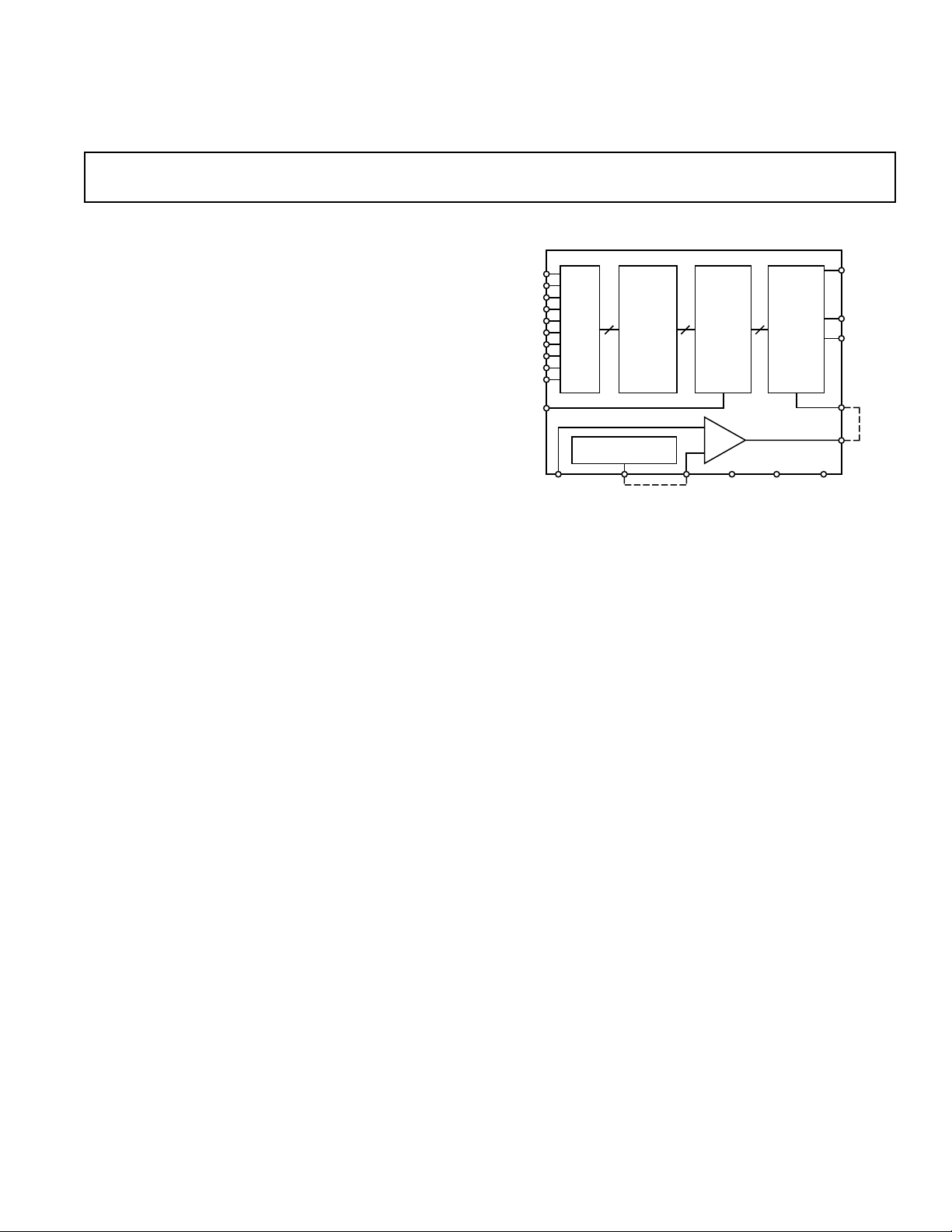
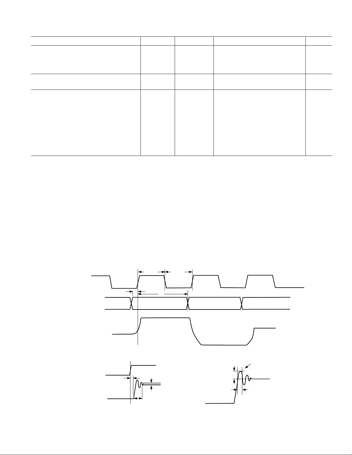
CLOCK
D/A Converter
AD9731
FUNCTIONAL BLOCK DIAGRAM
ANALOG
–V
S
ANALOG
RETURN
IOUT
IOUT
REF IN
AMP OUT
D9
D8
D7
D6
TTL
D5
DRIVE
D4
LOGIC
D3
D2
D1
D0
R
SET
DECODERS
AND
DRIVERS
INTERNAL VOLTAGE
REFERENCE
REF OUT CONTROL
AMP IN
REGISTER
CONTROL
AMP
DIGITAL
–V
S
SWITCH
NETWORK
DIGITAL
+V
S
GENERAL DESCRIPTION
The AD9731 is a 10-bit, 170 MSPS, bipolar D/A converter that
is optimized to provide high dynamic performance, yet offer
lower power dissipation and more economical pricing than
afforded by previous bipolar high performance DAC solutions.
The AD9731 was designed primarily for demanding communications systems applications where wideband spurious-free
dynamic range (SFDR) requirements are strenuous and could
previously only be met by using a high performance DAC such
as the industry-standard AD9721. The proliferation of digital
communications into basestation and high volume subscriberend markets has created a demand for excellent DAC performance delivered at reduced levels of power dissipation and cost.
The AD9731 is the answer to that demand.
Optimized for direct digital synthesis (DDS) waveform reconstruction, the AD9731 provides 50 dB of wideband harmonic
suppression over a dc-to-65 MHz analog output bandwidth.
This signal bandwidth addresses the transmit spectrum in many
of the emerging digital communications applications where
signal purity is critical. Narrowband, the AD9731 provides an
SFDR of greater than 79 dB. This excellent wideband and
narrowband ac performance, coupled with a lower pricing structure, make the AD9731 the optimum high performance DAC
value.
The AD9731 is packaged in 28-lead SOIC (same footprint
as the industry standard AD9721) and super space-saving
28-lead SSOP; both are specified to operate over the extended
industrial temperature range of –40°C to +85°C.
REV. A
Information furnished by Analog Devices is believed to be accurate and
reliable. However, no responsibility is assumed by Analog Devices for its
use, nor for any infringements of patents or other rights of third parties
which may result from its use. No license is granted by implication or
otherwise under any patent or patent rights of Analog Devices.
One Technology Way, P.O. Box 9106, Norwood, MA 02062-9106, U.S.A.
Tel: 781/329-4700 World Wide Web Site: http://www.analog.com
Fax: 781/326-8703 © Analog Devices, Inc., 1999
Page 2

5/27/99 8 PM
AD9731–SPECIFICATIONS
(+VS = +5 V, –VS = –5.2 V, CLOCK = 125 MHz, R
V
= –1.25 V, unless otherwise noted.)
REF
= 1.96 k⍀ for 20.4 mA I
SET
OUT
,
Parameter Temp Test Level Min Typ Max Units
RESOLUTION 10 Bits
THROUGHPUT RATE +25°C IV 165 170 MHz
DC ACCURACY
Differential Nonlinearity +25°C I 0.25 1 LSB
Full VI 0.35 1.5 LSB
Integral Nonlinearity +25°C I 0.6 1 LSB
Full VI 0.7 1.5 LSB
INITIAL OFFSET ERROR
Zero-Scale Offset Error +25°C I 35 70 µA
Full VI 40 100 µA
+25°C I 2.5 5 % FS
Full-Scale Gain Error
1
Full VI 2.5 5 % FS
Offset Drift Coefficient V 0.04 µA/°C
REFERENCE/CONTROL AMP
Internal Reference Voltage
Internal Reference Voltage Drift Full IV 100 µV/°C
Internal Reference Output Current
2
3
+25°C I –1.35 –1.25 –1.15 V
Full VI –50 +500 µA
Amplifier Input Impedance +25°CV 50 kΩ
Amplifier Bandwidth +25°C V 2.5 MHz
4, 6
4
5
+25°C V 75 MHz
+25°CV 20 mA
REFERENCE INPUT
Reference Input Impedance +25°C V 4.6 kΩ
Reference Multiplying Bandwidth
OUTPUT PERFORMANCE
Output Current
Output Compliance +25°C IV –1.5 +3 V
Output Resistance +25°C V 240 Ω
Output Capacitance +25°CV 5 pF
Voltage Settling Time to 1/2 LSB (t
Propagation Delay (t
Glitch Impulse
9
Output Slew Rate
Output Rise Time
Output Fall Time
8
)
PD
10
10
10
ST
7
)
+25°C V 3.8 ns
+25°C V 2.9 ns
+25°C V 4.1 pVs
+25°C V 400 V/µs
+25°CV 1 ns
+25°CV 1 ns
DIGITAL INPUTS
Input Capacitance Full IV 2 pF
Logic “1” Voltage Full VI 2.0 V
Logic “0” Voltage Full VI 0.8 V
Logic “1” Current +25°CVI 8 50 µA
Logic “0” Current +25°C VI 30 100 µA
Minimum Data Setup Time (t
Minimum Data Hold Time (t
11
)
S
12
)
H
+25°C IV 1.2 2 ns
Full IV 1.5 2.5 ns
+25°C IV 0.1 1.0 ns
Full IV 0.1 1.0 ns
Clock Pulsewidth Low (pw
Clock Pulsewidth High (pw
SFDR PERFORMANCE (Wideband)
2 MHz A
10 MHz A
20 MHz A
40 MHz A
65 MHz A
70 MHz A
OUT
OUT
OUT
OUT
(Clock = 170 MHz) +25°CV 50 dB
OUT
(Clock = 170 MHz) +25°CV 47 dB
OUT
) +25°CIV 2 ns
MIN
) +25°CIV 2 ns
MAX
13
+25°CV 66 dB
+25°CV 62 dB
+25°CV 61 dB
+25°CV 55 dB
–2–
REV. A
Page 3
5/27/99 8 PM
AD9731
Parameter Temp Test Level Min Typ Max Units
SFDR PERFORMANCE (Narrowband)
2 MHz; 2 MHz Span +25°CV 79 dB
25 MHz, 2 MHz Span +25°CV 61 dB
10 MHz, 5 MHz Span (Clock = 170 MHz) +25°CV 73 dB
INTERMODULATION DISTORTION
F1 = 800 kHz, F2 = 900 kHz +25°CV 58 dB
POWER SUPPLY
15
Digital –V Supply Current +25°C I 27 37 mA
Analog –V Supply Current +25°C I 45 53 mA
Digital +V Supply Current +25°C I 13 20 mA
Power Dissipation +25°C V 439 mW
PSRR +25°C V 100 µA/V
NOTES
1
Measured as an error in ratio of full-scale current to current through R
2
Internal reference voltage is tested under load conditions specified in Internal Reference Output current specification.
3
Internal reference output current defines load conditions applied during Internal Reference Voltage test.
4
Full-scale current variations among devices are higher when driving REFERENCE IN directly.
5
Frequency at which a 3 dB change in output of DAC is observed; R
6
Based on IFS = 32 (CONTROL AMP IN/R
7
Measured as voltage settling at midscale transition to ±0.1%; RL = 50 Ω.
8
Measured from 50% point of rising edge of CLOCK signal to 1/2 LSB change in output signal.
9
Peak glitch impulse is measured as the largest area under a single positive or negative transient.
10
Measured with R
11
Data must remain stable for specified time prior to rising edge of CLOCK.
12
Data must remain stable for specified time after rising edge of CLOCK.
13
SFDR is defined as the difference in signal energy between the full-scale fundamental signal and worst case spurious frequencies in the output spectrum window.
The frequency span is dc-to-Nyquist unless otherwise noted.
14
Intermodulation distortion is the measure of the sum and difference products produced when a two-tone input is driven into the DAC. The distortion products
created will manifest themselves at sum and difference frequencies of the two tones.
15
Supply voltages should remain stable within ±5% for nominal operation.
Specifications subject to change without notice.
= 50 Ω and DAC operating in latched mode.
L
13
14
Full VI 27 42 mA
Full VI 45 66 mA
Full VI 15 22 mA
Full V 449 mW
(640 µA nominal); ratio is nominally 32. DAC load is virtual ground.
SET
= 50 Ω; 100 mV modulation at midscale.
) when using internal control amplifier. DAC load is virtual ground.
SET
L
CLOCK
DATA
ANALOG OUTPUT
ANALOG OUTPUT
t
S
CODE 1
DATA
CODE 1
DETAIL OF SETTLING TIME
CLOCK
t
PD
t
ST
pw
MIN
CODE 2
SPECIFIED
ERROR BAND
t
H
DATA
CODE 2
pw
MAX
Figure 1. Timing Diagrams
CODE 3
DATA
CODE 3
GLITCH AREA =
1/2 HEIGHT 3 WIDTH
H
W
CODE 4
DATA
CODE 4
–3–REV. A
Page 4
AD9731
ABSOLUTE MAXIMUM RATINGS*
Analog Output . . . . . . . . . . . . . . . . . . . . . . . . . . . . –VS to +V
S
+VS . . . . . . . . . . . . . . . . . . . . . . . . . . . . . . . . . . . . . . . . . +6 V
Digital Inputs . . . . . . . . . . . . . . . . . . . . . . . . . . –0.7 V to +V
S
–VS . . . . . . . . . . . . . . . . . . . . . . . . . . . . . . . . . . . . . . . . . –7 V
Analog Output Current . . . . . . . . . . . . . . . . . . . . . . . . 30 mA
Control Amplifier Input Voltage Range . . . . . . . . . 0 V to –4 V
Reference Input Voltage Range . . . . . . . . . . . . . . . . 0 V to –V
S
Maximum Junction Temperature . . . . . . . . . . . . . . . .+150°C
Operating Temperature Range . . . . . . . . . . . –40°C to +85°C
Internal Reference Output Current . . . . . . . . . . . . . . . 500 µA
Lead Temperature (10 sec Soldering) . . . . . . . . . . . . .+300°C
Storage Temperature . . . . . . . . . . . . . . . . . . –65°C to +165°C
Control Amplifier Output Current . . . . . . . . . . . . . ±2.5 mA
*Absolute maximum ratings are limiting values, to be applied individually, and
beyond which the serviceability of the circuit may be impaired. Functional
operability under any of these conditions is not necessarily implied. Exposure of
absolute maximum rating conditions for extended periods of time may affect
device reliability.
ORDERING GUIDE
Temperature Package Package
Model Range Description Options
AD9731BR –40°C to +85°C 28-Lead Wide Body (SOIC) R-28
AD9731BRS –40°C to +85°C 28-Lead Shrink Small (SSOP) RS-28
AD9731-PCB 0°C to +70°C PCB
EXPLANATION OF TEST LEVELS
Test Level Definition
I 100% Production Tested.
II The parameter is 100% production tested at
+25°C; sampled at temperature production.
III Sample Tested Only.
IV Parameter is guaranteed by design and character-
ization testing.
V Parameter is a typical value only.
VI All devices are 100% production tested at +25°C;
guaranteed by design and characterization testing
for industrial temperature range devices.
CAUTION
ESD (electrostatic discharge) sensitive device. Electrostatic charges as high as 4000 V readily
accumulate on the human body and test equipment and can discharge without detection.
Although the AD9731 features proprietary ESD protection circuitry, permanent damage may
occur on devices subjected to high energy electrostatic discharges. Therefore, proper ESD
precautions are recommended to avoid performance degradation or loss of functionality.
WARNING!
ESD SENSITIVE DEVICE
–4–
REV. A
Page 5
AD9731
PIN FUNCTION DESCRIPTION
Pin # Pin Name Pin Description
1 D9(MSB) Most significant data bit of digital input word.
2–9 D8–D1 Eight bits of 10-bit digital input word.
10 D0(LSB) Least significant data bit of digital input word.
11 CLOCK TTL-compatible edge-triggered latch enable signal for on-board registers.
12, 13 NC No internal connection to this pin.
14 DIGITAL +V
S
15, 18, 28 GND Converter Ground.
16 DIGITAL –V
17 R
SET
S
19 ANALOG RETURN Analog Return. This point and the reference side of the DAC load resistors should be con-
20 I
21 I
22 ANALOG –V
OUT
OUTB
S
23 REF IN Normally connected to CONTROL AMP OUT (Pin 24). Direct line to DAC current
24 CONTROL AMP OUT Normally connected to REF IN (Pin 23). Output of internal control amplifier which pro-
25 REF OUT Normally connected to CONTROL AMP IN (Pin 26). Internal voltage reference, nomi-
26 CONTROL AMP IN Normally connected to REF Out (Pin 25) if not connected to external reference.
27 DIGITAL –V
S
+5 V supply voltage for digital circuitry.
–5.2 V supply voltage for digital circuitry.
Connection for external reference set resistor; nominal 1.96 kΩ. Full-scale output current =
32 (Control Amp in V/R
SET
).
nected to the same potential (nominally ground).
Analog current output; full-scale current occurs with a digital word input of all “1s.” With
external load resistor, output voltage = I
(R
OUT
LOAD储RINTERNAL
). R
INTERNAL
is nominally
240 Ω.
Complementary analog current output; full-scale current occurs with a digital word input
of all “0s.”
Negative analog supply, nominally –5.2 V.
source network. Voltage changes (noise) at this point have a direct effect on the full-scale
output current of the DAC. Full-scale current output = 32 (CONTROL AMP IN/R
SET
)
when using the internal amplifier. DAC load is virtual ground.
vides a reference for the current switch network.
nally –1.25 V.
Negative digital supply, nominally –5.2 V.
D9(MSB)
D0(LSB)
CLOCK
DIGITAL +V
PIN CONFIGURATION
1
2
D8
3
D7
4
D6
5
D5
6
D4
AD9731
7
D3
TOP VIEW
(Not to Scale)
8
D2
9
D1
10
11
12
NC
13
NC
14
S
NC = NO CONNECT
28
GND
27
DIGITAL –V
26
CONTROL AMP IN
25
REF OUT
24
CONTROL AMP OUT
23
REF IN
22
ANALOG –V
21
I
OUTB
20
I
OUT
19
ANALOG RETURN
18
GND
17
R
SET
16
DIGITAL –V
15
GND
–5–REV. A
S
S
S
Page 6
AD9731
–Typical Performance Characteristics
80
75
70
65
SFDR – dB
60
55
50
10
20 30 40 50 60 70 80
A
– MHz
OUT
Figure 2. Narrowband SFDR (Clock = 170 MHz) vs.
A
Frequency
OUT
85
80
75
70
65
SFDR – dB
60
60
55
50
SFDR – dB
45
40
20 18 10 6 2
Figure 5. SFDR vs. I
0.4
0.3
0.2
0.1
0
LSB
–0.1
–0.2
16 14 12 8 4
OUT
I
– mA
OUT
(Clock =125 MHz/A
= 40 MHz)
OUT
55
50
10
20 30 40 50 60
A
– MHz
OUT
Figure 3. Narrowband SFDR (Clock = 125 MHz) vs.
Frequency
A
OUT
65
60
55
SFDR – dB
50
45
40
20 30 40 50 60
10
A
– MHz
OUT
Figure 4. Wideband SFDR (170 MHz Clock) vs. A
70 80 90
OUT
–0.3
–0.4
Figure 6. Typical Differential Nonlinearity Performance
(DNL)
0.6
0.4
0.2
0
LSB
–0.2
–0.4
–0.6
Figure 7. Typical Integral Nonlinearity Performance (INL)
–6–
REV. A
Page 7
1
–10
–20
–30
–40
–50
–60
–70
–80
–90
–100
ENCODE = 125MHz
A
OUT
= 40MHz
SPAN = 62.5MHz
1
1
1AP
0Hz
START
6.25MHz 62.5MHz
STOP
0
–10
–20
–30
–40
–50
–60
–70
–80
–90
1
1
1AP
0Hz
START
8.5MHz 85MHz
STOP
–10
–20
–30
–40
–50
–60
–70
–80
–90
–100
0Hz
START
ENCODE = 125MHz
A
= 2MHz
OUT
SPAN = 62.5MHz
6.25MHz 62.5MHz
Figure 8. Wideband SFDR 2 MHz A
1
STOP
; 125 MHz Clock
OUT
1AP
Figure 11. Wideband SFDR 40 MHz A
AD9731
; 125 MHz Clock
OUT
–10
–20
–30
–40
–50
–60
–70
–80
–90
–100
START
0Hz
1
Figure 9. Wideband SFDR 10 MHz A
–10
–20
–30
–40
–50
–60
–70
–80
–90
–100
0Hz
START
Figure 10. Wideband SFDR 20 MHz A
1
ENCODE = 125MHz
A
= 10MHz
OUT
SPAN = 62.5MHz
1AP
1
6.25MHz 62.5MHz
; 125 MHz Clock
OUT
ENCODE = 125MHz
A
= 20MHz
OUT
SPAN = 62.5MHz
6.25MHz 62.5MHz
; 125 MHz Clock
OUT
PRN
STOP
1AP
1
STOP
Figure 12. Wideband SFDR 65 MHz A
–10
–20
–30
–40
–50
–60
–70
–80
–90
–100
0Hz
START
ENCODE = 170MHz
A
= 70MHz
OUT
SPAN = 85MHz
8.5MHz 85MHz
Figure 13. Wideband SFDR 70 MHz A
–7–REV. A
; 170 MHz Clock
OUT
1
1AP
1
STOP
; 170 MHz Clock
OUT
Page 8
AD9731
–10
–20
–30
–40
–50
–60
–70
–80
–90
–100
0Hz
START
1
1
ENCODE = 125MHz
1 = 800kHz
A
OUT
2 = 900kHz
A
OUT
SPAN = 2MHz
200kHz 2MHz
1AP
STOP
Figure 14. Wideband Intermodulation Distortion
F1 = 800 kHz; F2 = 900 kHz; 125 MHz Clock; Span = 2 MHz
1
–10
–20
–30
–40
–50
–60
–70
–80
–90
–100
START
0Hz
ENCODE = 125MHz
1 = 800kHz
A
OUT
2 = 900kHz
A
OUT
SPAN = 62.5MHz
1
6.25MHz 62.5MHz
1AP
PRN
STOP
Figure 15. Wideband Intermodulation Distortion F1 =
800 kHz; F2 = 900 kHz; 125 MHz Clock; Span = 62.5 MHz
THEORY AND APPLICATIONS
The AD9731 high speed digital-to-analog converter utilizes
most significant bit decoding and segmentation techniques to
reduce glitch impulse and deliver high dynamic performance
on lower power consumption than previous bipolar DAC
technologies.
The design is based on four main subsections: the decoder/
driver circuits, the edge-triggered data register, the switch network and the control amplifier. An internal bandgap reference is
included to allow operation of the device with minimum external support components.
Digital Inputs/Timing
The AD9731 has TTL/high speed CMOS-compatible singleended inputs for data inputs and clock. The switching threshold
is +1.5 V.
In the decoder/driver section, the three MSBs are decoded to
seven “thermometer code” lines. An equalizing delay is included
for the seven least significant bits and the clock signals. This
delay minimizes data skew and data setup and hold times at the
register inputs.
The on-board register is rising-edge triggered and should be
used to synchronize data to the current switches by applying a
pulse with proper data setup and hold times as shown in the
timing diagram. Although the AD9731 is designed to provide
isolation of the digital inputs to the analog output, some coupling of digital transitions is inevitable. Digital feedthrough can
be minimized by forming a low-pass filter at the digital input by
using a resistor in series with the capacitance of each digital
input. This common high speed DAC application technique has
the effect of isolating digital input noise from the analog output.
References
The internal bandgap reference, control amplifier and reference
input are pinned out to provide maximum user flexibility in
configuring the reference circuitry for the AD9731. When using
the internal reference, REF OUT (Pin 25) should be connected
to CONTROL AMP IN (Pin 26). CONTROL AMP OUT (Pin
24) should be connected to REF IN (Pin 23). A 0.1 µF ceramic
capacitor connected from Pin 23 to Analog –V
(Pin 22) im-
S
proves settling time by decoupling switching noise from the
current sink baseline. A reference current cell provides feedback
to the control amplifier by sinking current through R
(Pin 17).
SET
Full-scale current is determined by CONTROL AMP IN and
R
according to the following equation:
SET
I
(FS) = 32(CONTROL AMP IN/R
OUT
SET
)
The internal reference is nominally –1.25 V with a tolerance of
±8% and typical drift over temperature of 100 ppm/°C. If
greater accuracy or temperature stability is required, an external
reference can be used. The AD589 reference features 10 ppm/°C
drift over the 0°C to +70°C temperature range.
Two modes of multiplying operation are possible with the
AD9731. Signals with bandwidths up to 2.5 MHz and input
swings from –0.6 V to –1.2 V can be applied to the CONTROL
AMP IN pin as shown in Figure 16. Because the control ampli-
fier is internally compensated, the 0.1 µF capacitor discussed
above can be reduced to maximize the multiplying bandwidth.
However, it should be noted that output settling time, for
changes in the digital word, will be degraded.
AD9731
R
SET
CONTROL
AMP IN
CONTROL
AMP OUT
REFERENCE IN
S
–0.6 TO –1.2V
2.5MHz TYPICAL
R
SET
R
T
0.1mF
ANALOG –V
Figure 16. Low Frequency Multiplying Circuit
–8–
REV. A
Page 9
AD9731
The REFERENCE IN pin can also be driven directly for wider
bandwidth multiplying operation. The analog signal for this mode
of operation must have a signal swing in the range of –3.3 V to
–4.25 V. This can be implemented by capacitively coupling into
REFERENCE IN a signal with a dc bias of –3.3 V (I
22.5 mA) to –4.25 V (I
≈ 3 mA), as shown in Figure 17, or
OUT
OUT
≈
by dividing REFERENCE IN with a low impedance op amp
whose signal swing is limited to the stated range.
NOTE: When using an external reference, the external reference voltage must be applied prior to applying –V
AD9731
APPROX
–3.8V
REFERENCE IN
–V
S
–V
S
.
S
Figure 17. Wideband Multiplying Circuit
Analog Output
The switch network provides complementary current outputs
I
OUT
and I
. The design of the AD9731 is based on statisti-
OUTB
cal current source matching, which provides a 10-bit linearity
without trim. Current is steered to either I
OUT
or I
OUTB
in proportion to the digital input word. The sum of the two currents is
always equal to the full-scale output current minus 1 LSB. The
current can be converted to a voltage by resistive loading as
shown in the block diagram. Both I
OUT
and I
OUTB
should be
equally loaded for best overall performance. The voltage that is
developed is the product of the output current and the value of
the load resistor.
An operational amplifier can also be used to perform the I-to-V
conversion of the DAC output. Figure 18 shows an example of a
circuit that uses the AD9617, a high speed, current feedback
amplifier. The resistor values in Figure 18 provide a 4.096 V
swing, centered at ground, at the output of the AD9617 amplifier.
10kV
CONTROL
AMP IN
I
OUT
AD9731
I
OUTB
10kV
1/2
AD708
I
FS
R
25V
L
25V
R
25V
FF
R1
200V
I
FS
R2
100V
AD9617
R
FB
400V
±2048V
V
OUT
1/2
AD708
REF
OUT
Figure 18. I-to-V Conversion Using a Current Feedback
Amplifier
EVALUATION BOARD
The performance characteristics of the AD9731 make it ideally
suited for direct digital synthesis (DDS) and other waveform
synthesis applications. The AD9731 evaluation board provides a
platform for analyzing performance under optimum layout conditions. The AD9731 also provides a reference for high speed
circuit board layout techniques.
–9–REV. A
Page 10
AD9731
C4
0.1mF
BNC1J2
R16
50V
AGND
R15
AGND
1918171615
OUTIOUT
I
ANA RETURN
9
1011121314
U12
U11 R10
U10 R9 U13
25V
AGND
–V DIG
S
SET
GND
R
GND1
DIGITAL –V
DAC CLOCK
NC1
NC2
+5 DIG
+V DIG
R14
1960V
AGND
DGND
–V ANA
C2
10mF
C1
DGND
–V DIG
BNC
DGND
C5
0.1mF
+V DIG
+V DIG+V DIG
4
PWR
Y1
PWR3
–V DIG
3
2
OUT
GND
OPTIONAL
OSCILLATOR
GND–V+V
DGND
+V DIG
DGND
282726252423222120
S
GND3
DIGITAL –V
U1
AD9731
D1
D2D3D4D5D6D7D8D9D10
12345
R1 U21
NOTE: R1–R10 = 50V
U3 R2 U20
U2
0.1mF
REF IN
REF OUT
ANALOG –V
CONTROL AMP IN
CONTROL AMP OUT
678
U17
U4 R3 U19
U5 R4 U18
U6 R5
U7 R6 U16
U8 R7 U15
S
U14
U9 R8
C3
+VD
–VA
C9
C8
C7
–V DIG
10mF
C6
0.1mF
AGND DGND
0.1mF
0.1mF
10mF
DGND
4.9kV
OPTIONAL
RP2
4.9kV
OPTIONAL
RP1
E1 E2
CON1
C37DRPF
+VD
2018161412
–12V
+5V1
+5V2
+12V
–VD
E4E3
29
–5V
1
2
3
4
5
11
12
13
14
P1P1P1P1P1P1P1P1P1P1P1P1P1P1P1P1P1P1P1
DGND
BNC1
28272625242322
PC0
PC1
PC2
PC3
J1
+V DIG
PC4
PC5
PC6
R12
PC7
50V
R11
4.9kV
211917
GND1
GND2
15
BNC
GND3
16
DGND
6
17
E6E5
E7
9876543
10
PB0
PB1
E8
7
PB2
18
E9 E10
PB3
8
PB4
19
PB5
9
PB6
20
R13
PB7
10
P1
50V
DGND
151311
GND4
GND5
DGND
DGND
DGND
37363534333231
PA0
GND6
PA1
PA2
PA3
PA4
PA5
PA6
CLOCK SWITCH MATRIX
2
1
30
II
IEN
PA7
JUMPER SOURCE NOTES
E5 TO E7 CON 1 PIN 10 COMPUTER PROVIDES CLOCK
E6 TO E8 J1 BNC REMOVE Y1
E6 TO E8 Y1 REMOVE R12
E8 TO E10 DG2020 DATA
EXT. CLK TO E7 GENERATOR
EXT. GND TO E9
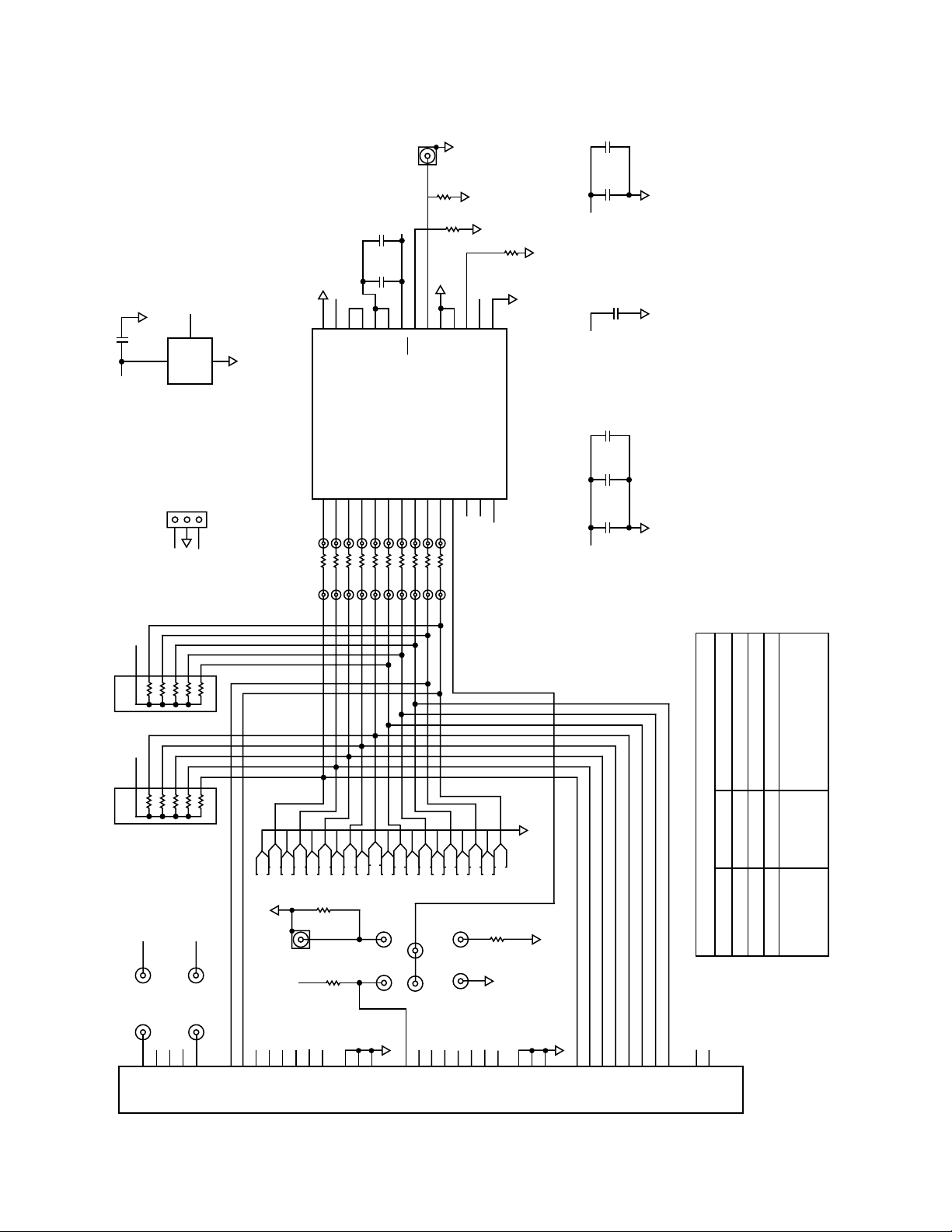
Figure 19. AD9731-PCB Evaluation Board Schematic
–10–
REV. A
Page 11
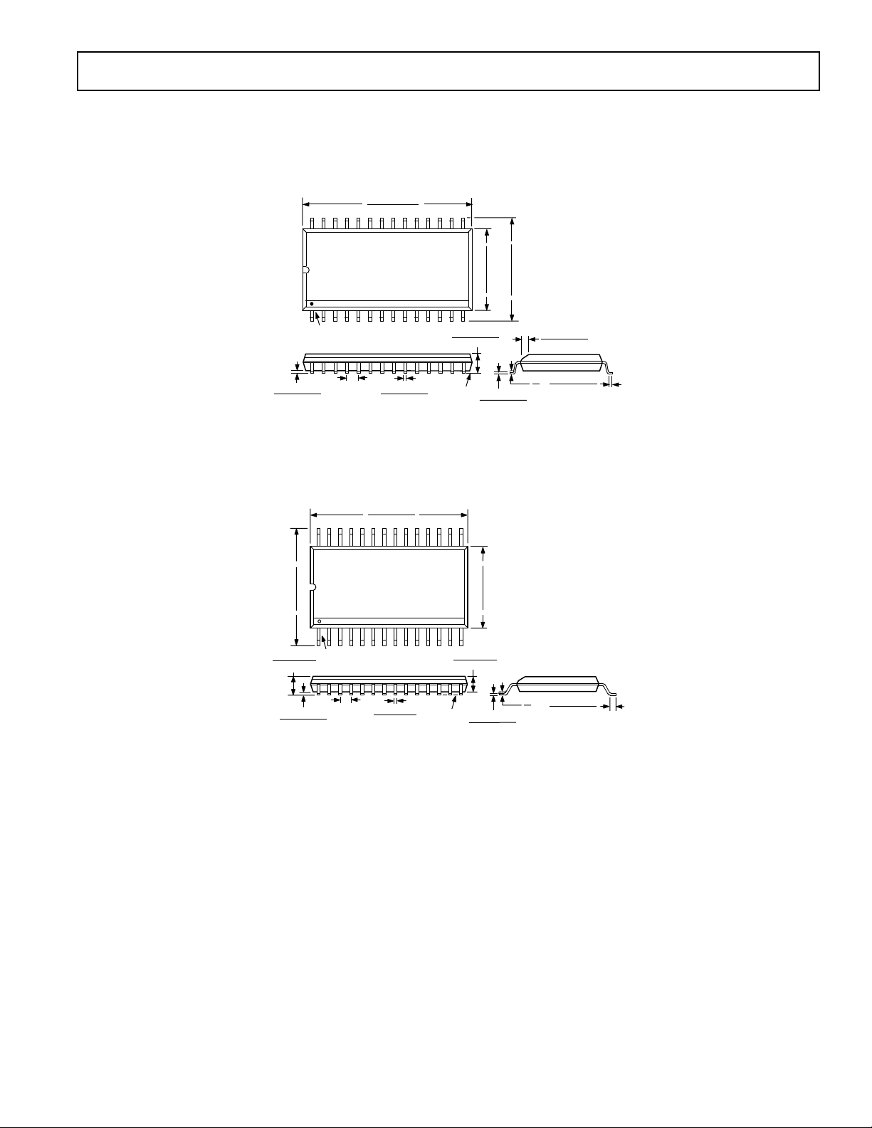
OUTLINE DIMENSIONS
Dimensions shown in inches and (mm).
28-Lead SOIC Wide Body (SOIC)
(R-28)
0.7125 (18.10)
0.6969 (17.70)
28 15
141
0.2992 (7.60)
0.2914 (7.40)
0.4193 (10.65)
0.3937 (10.00)
AD9731
0.0118 (0.30)
0.0040 (0.10)
0.311 (7.9)
0.301 (7.64)
0.078 (1.98)
0.068 (1.73)
0.008 (0.203)
0.002 (0.050)
PIN 1
0.0500
(1.27)
BSC
0.0192 (0.49)
0.0138 (0.35)
0.1043 (2.65)
0.0926 (2.35)
SEATING
PLANE
0.0125 (0.32)
0.0091 (0.23)
28-Lead Shrink Small Outline (SSOP)
(RS-28)
0.407 (10.34)
0.397 (10.08)
28 15
0.212 (5.38)
0.205 (5.21)
141
PIN 1
0.0256
(0.65)
BSC
0.015 (0.38)
0.010 (0.25)
0.066 (1.67)
SEATING
PLANE
0.07 (1.79)
0.009 (0.229)
0.005 (0.127)
0.0291 (0.74)
0.0098 (0.25)
8°
0°
8°
0°
x 45°
0.0500 (1.27)
0.0157 (0.40)
0.03 (0.762)
0.022 (0.558)
–11–REV. A
 Loading...