

Page 1

14-Bit, 600+ MSPS
Preliminary Technical Data
FEATURES
600+ MSPS DAC update rate
16/14/12/10-bit resolution family
LVDS interface with built-in 100-termination resistors
Single data rate and double data rate capability
Excellent dynamic performance
SFDR = 63 dBc at 140 MHz
IMD = 73 dBc at 140 MHz
Differential current outputs: 2 mA to 20 mA
–40°C to +85°C temperature range operation
On-chip 1.20 V reference
Package: 80-lead thermally-enhanced TQFP
Versatile clock and data interface
APPLICATIONS
Instrumentation and test
Wideband communications systems
Point-to-point wireless
LMDS
PA linearization
High resolution displays
PRODUCT DESCRIPTION
The AD9725 is a 14-bit digital-to-analog converter (DAC) that
utilizes an LVDS interface to achieve conversion rates in excess
of 600 MSPS. It is in a family of pin compatible converters that
offers selection of 10-bit, 12-bit, 14-bit, and 16-bit resolution
grades. All of the devices share the same interface options, small
outline package, and pinout, providing an upward or downward
component selection path based on performance, resolution
and cost.
D/A Converter
AD9725
FUNCTIONAL BLOCK DIAGRAM
CALIBRATION REFERENCE
DB[13:0]+
DB[13:0]–
DDR
DATACLK_IN+
DATACLK_IN–
REXT
DATACLK_OUT+
DATACLK_OUT–
CLK+
CLK–
DATA
FORMATTER
DATA CLOCK
FORMATTER
DATA SYNC.
CLOCK DISTRIBUTIO N
AND CONTROL
14-BIT
DAC
SPI
Figure 1
PRODUCT HIGHLIGHTS
Ultralow noise and intermodulation distortion (IMD) enable
high quality waveform synthesis at intermediate frequencies up
to 200 MHz.
LVDS receivers support SDR or DDR modes, with the maximum conversion rate exceeding 600 MSPS.
Manufactured on a CMOS process, the AD9725 uses a proprietary switching technique that enhances dynamic performance.
The current output of the AD9725 can be easily configured for
various single-ended or differential circuit topologies.
FSADJ
REFIO
IOUTA
IOUTB
SDIO
SDO/SYNC _ALRM
CSB
SCLK/SYN C_UPD
RESET
04540-0-001
Rev. PrA
Information furnished by Analog Devices is believed to be accurate and reliable.
However, no responsibility is assumed by Analog Devices for its use, nor for any
infringements of patents or other rights of third parties that may result from its use.
Specifications subject to change without notice. No license is granted by implication
or otherwise under any patent or patent rights of Analog Devices. Trademarks and
registered trademarks are the property of their respective owners.
One Technology Way, P.O. Box 9106, Norwood, MA 02062-9106, U.S.A.
Tel: 781.329.4700 www.analog.com
Fax: 781.326.8703 © 2004 Analog Devices, Inc. All rights reserved.
Page 2

AD9725
TABLE OF CONTENTS
Preliminary Technical Data
Specifications..................................................................................... 3
DC Specifications ......................................................................... 3
AC Specifications.......................................................................... 4
Digital Specifications ................................................................... 5
Digital Timing Information........................................................ 5
Absolute Maximum Ratings............................................................ 6
Pin Configuration and Function Description .............................. 7
Serial Port Interface Register Maps................................................ 9
Definitions....................................................................................... 11
Typical Performance Curves......................................................... 12
Theory of Operation ...................................................................... 13
LVDS Inputs................................................................................ 13
Data Synchronization Circuitry............................................... 13
Internal Reference and Full-Scale Output Current................ 13
Analog Output............................................................................ 14
SPI Port Control......................................................................... 14
General Operation of the Serial Port Interface ...................... 14
Instruction Byte.......................................................................... 14
Serial Port Interface Pin Description....................................... 14
Notes on Serial Port Operation................................................ 15
Outline Dimension......................................................................... 16
Ordering Guide .......................................................................... 16
Rev. PrA | Page 2 of 16
Page 3

Preliminary Technical Data
AD9725
SPECIFICATIONS
DC SPECIFICATIONS
Table 1. T
otherwise noted. Specifications subject to change without notice
Parameter Min Typ Max Unit
Resolution 14 Bits
DC Accuracy
Integral Nonlinearity ±1.5 LSB
Differential Nonlinearity ±0.75 LSB
Analog Output
Offset Error –1 1 %FSR
Gain Error %FSR
Full Scale Output Current 20 1.26 mA
Output Compliance Range 1.14 V
Output Resistance TBD 1.25 kW
Output Capacitance 0.1 TBD pF
Reference Output
Reference Voltage 1.2 V
Reference Output Current 100 nA
Reference Input
Reference Input Compliance Range V
Reference Input Resistance 5 kW
Small Signal Bandwidth 0.5 MHz
Temperature Coefficients
Offset Drift TBD ppm of FSR/ºC
Gain Drift (With Internal Reference) TBD ppm of FSR/ºC
Reference Voltage Drift TBD ppm/ºC
Power Supply1
AVDD1, AVDD2
Voltage Range 3.3 V
Analog Supply Current (I
ADVDD
Voltage Range 2.5 V
ACVDD mA
Voltage Range 2.5 V
Analog Supply Current ( I
CLKVDD
Voltage Range 2.5 V
Clock Supply Current (I
DVDD
Voltage Range 2.5 V
Digital Supply Current (I
DBVDD
Voltage Range 3.3 V
Digital Supply Current (I
Nominal Power Dissipation (P
Nominal Power Dissipation (P
1
Supply currents measured under the following conditions: f
2
Power dissipation measured under the following conditions: f
3
Power dissipation measured under the following conditions: f
MIN
to T
, AVDD1, AVDD2, DBVDD = 3.3 V, ADVDD, ACVDD, CLKVDD, DVDD = 2.5 V, I
MAX
+ I
AVDD1
ADVDD
) 20 mA
CLKVDD
) 69 mA
DVDD
DBVDD
) 51 mA
AVDD2
+ I
) 9 mA
ACVDD
) 20 mA
)2 479 mW
DIS
)3 1000 mW
DIS
= 200 MSPS, f
DAC
= 200 MSPS, f
DAC
= 600 MSPS, f
DAC
= 11 MHz, nominal power supply voltages
OUT
= 11 MHz, nominal power supply voltages
OUT
= 111 MHz, nominal power supply voltages
OUT
= 20 mA, unless
OUTFS
Rev. PrA | Page 3 of 16
Page 4

AD9725
Preliminary Technical Data
AC SPECIFICATIONS
Table 2. T
otherwise noted. Specifications subject to change without notice.
Parameter Typ Unit
Dynamic Performance
Max DAC Output Update Rate (DDR) 600 MSPS
Max DAC Output Update Rate (SDR) 440 MSPS
AC Linearity
Spurious Free Dynamic Range (SFDR) to Nyquist (f
f
f
f
f
f
f
f
f
f
Two Tone IMD to Nyquist (f
f
f
f
f
f
f
f
f
f
Noise Spectral Density (NSD)
f
f
f
f
CDMA2000 Adjacent Channel Leakage Ratio (ACLR)
f
f
f
WCDMA Adjacent Channel Leakage Ratio (ACLR), Single Carrier
f
f
f
f
WCDMA Adjacent Channel Leakage Ratio (ACLR), Four Carrier
f
f
to T
MIN
= 260 MSPS, f
DATA
= 260 MSPS, f
DATA
= 260 MSPS, f
DATA
= 400 MSPS, f
DATA
= 400 MSPS, f
DATA
= 400 MSPS, f
DATA
= 600 MSPS, f
DATA
= 600 MSPS, f
DATA
= 600 MSPS, f
DATA
= 300 MSPS, f
DATA
= 300 MSPS, f
DATA
= 300 MSPS, f
DATA
= 500 MSPS, f
DATA
= 500 MSPS, f
DATA
= 500 MSPS, f
DATA
= 600 MSPS, f
DATA
= 600 MSPS, f
DATA
= 600 MSPS, f
DATA
= 500 MSPS, f
DATA
= 500 MSPS, f
DATA
= 500 MSPS, f
DATA
= 500 MSPS, f
DATA
= 245.76 MSPS, IF = 61.44 MHz TBD dBc
DATA
= 491.52 MSPS, IF = 122.88 MHz TBD dBc
DATA
= 491.52 MSPS, IF = 190 MHz TBD dBc
DATA
= 184.32 MSPS, IF = 61.44 MHz 79 dBc
DATA
= 245.76 MSPS, IF= 61.44 MHz 79 dBc
DATA
= 491.52 MSPS, IF = 122.88 MHz 76 dBc
DATA
= 491.52 MSPS, IF = 190 MHz 74 dBc
DATA
= 184.32 MSPS, IF = 61.44 MHz, 69 dBc
DATA
= 368.64 MSPS, IF = 92.16 MHz 67 dBc
DATA
, AVDD1, AVDD2, DBVDD = 3.3 V, ADVDD, ACVDD, CLKVDD, DVDD = 2.5 V, I
MAZ
= 0 dBFS)
OUT
= 20 MHz 71 dBc
OUT
= 70 MHz 68 dBc
OUT
= 120 MHz 68 dBc
OUT
= 20 MHz 72 dBc
OUT
= 70 MHz 66 dBc
OUT
= 140 MHz 60 dBc
OUT
= 20 MHz TBD dBc
OUT
= 125 MHz TBD dBc
OUT
= 250 MHz TBD dBc
OUT
= f
OUT1
= 26 MHz, f
OUT1
= 100 MHz, f
OUT1
= 126 MHz, f
OUT1
= 26 MHz, f
OUT1
= 100 MHz, f
OUT1
= 126 MHz, f
OUT1
= 26 MHz, f
OUT1
= 126 MHz, f
OUT1
= 250 MHz, f
OUT1
= 20 MHz, 0 dBFS –162 dBm/Hz
OUT
= 20 MHz, –12 dBFS –165 dBm/Hz
OUT
= 120 MHz, 0 dBFS –151 dBm/Hz
OUT
= 120 MHz, –12 dBFS –161 dBm/Hz
OUT
= –6 dBFS)
OUT2
= 27 MHz 89 dBc
OUT2
= 101 MHz 80 dBc
OUT2
= 127 MHz 80 dBc
OUT2
= 27 MHz 90 dBc
OUT2
= 101 MHz 78 dBc
OUT2
= 127 MHz 76 dBc
OUT2
= 27 MHz TBD dBc
OUT2
= 127 MHz TBD dBc
OUT2
= 251 MHz TBD dBc
OUT2
OUTFS
= 20 mA, unless
Rev. PrA | Page 4 of 16
Page 5
Preliminary Technical Data
T
AD9725
DIGITAL SPECIFICATIONS
Table 3. T
otherwise noted. Specifications subject to change without notice.
Parameter Conditions Min Typ Max Unit
Digital Inputs VCM = 0.875 V to 1.575 V
Differential Logic ‘1’
Differential Logic ‘0’ –0.6 –0.1 V
Logic ‘1’ current 3.5 mA
Logic ‘0’ current 3.5 mA
Differential Input Resistance 100 W
Differential Input Capacitance 3 pF
Data Setup Time (tDS) 0.9 ns
Data Hold Time (tDH) –0.3 ns
Data Clock Output Delay ( t
Serial Control Bus
Maximum SCLK Frequency (fSCLK) 15 MHz
Minimum Clock Pulse Width High (t
Minimum Clock Pulse Width Low (t
Maximum Clock Rise/Fall Time 1 ms
Minimum Data/Chip Select Set Up Time (tDS) 25 ns
Minimum Data Hold Time (tDH) 0 ns
Maximum Data Valid Time (tDV) 30 ns
RESET Pulse Width 1.5 ns
Inputs (SDI, SDIO, SCLK, CSB)
Logic ‘1’ Voltage 2.1 3 V
Logic ‘0’ Voltage 0 0.9 V
Logic ‘1’ Current –10 +10 µA
Logic ‘0’ Current –10 +10 µA
Input Capacitance 5 pF
SDIO Output
Logic ‘1’ Voltage DRVDD–0.6 V
Logic ‘0’ Voltage 0.4 V
Logic ‘1’ Current 30 50 mA
Logic ‘0’ Current 30 50 mA
MIN
to T
, AVDD1, AVDD2, DBVDD = 3.3 V, ADVDD, ACVDD, CLKVDD, DVDD = 2.5 V , I
MAX
(put into footnote, and delete
0.1 0.6 V
column?)
) 2.4 ns
DCO
) 30 ns
PWH
) 30 ns
PWL
= 20 mA, unless
OUTFS
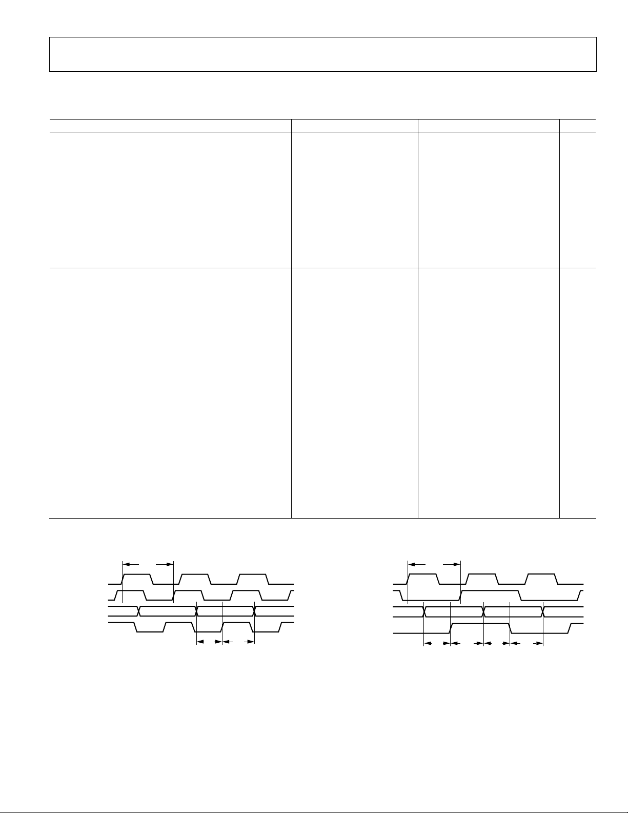
DIGITAL TIMING INFORMATION
t
DCO
CLK
DATACLK_OU
DB[15:0]
DATACLK_IN
Figure 2. Single Datarate (SDR) Mode
t
DCO
CLK
DATACLK_OUT
DB[15:0]
DATACLK_IN
t
t
DH
DS
04540-0-002
Rev. PrA | Page 5 of 16
t
t
DS
Figure 3. Double Datarate (DDR) Mode
t
DH
DS
t
DH
04540-0-003
Page 6

AD9725
Preliminary Technical Data
ABSOLUTE MAXIMUM RATINGS
Parameter With Respect to Min Max Unit
AVDD1, AVDD2, DBVDD ACOM1, ACOM2, DBCOM –0.3 TBD V
ADVDD, ACVDD, CLKVDD, DVDD
ACOM1, ACOM2, DBCOM ACOM1, ACOM2, DBCOM –0.3 +0.3 V
ADCOM, ACCOM, CLKCOM, DCOM
REFIO, FSDAJ ACOM1 –0.3 AVDD1 + 0.3 V
IOUTA, IOUTB ACOM1 –1 AVDD1 + 0.3 V
DB0-DB15, DB0-DB15 DBCOM –0.3 DBVDD + 0.3 V
DATACLKOUT, DATACLKOUT DBCOM –0.3 DBVDD + 0.3 V
REXT, CLK+, CLK- CLKCOM –0.3 CLKVDD + 0.3 V
SDO/SYNC_ALRM, SDIO, CSB DBCOM –0.3 DBVDD + 0.3 V
SCLK/SYNC, RESET DBCOM –0.3 DBVDD + 0.3 V
DDR, SPI_DIS ADCOM –0.3 ADVDD + 0.3 V
Stresses above those listed under Absolute Maximum Ratings may cause permanent damage to the device. This is a stress rating only;
functional operation of the device at these or any other conditions above those listed in the operational sections of this specification is not
implied. Exposure to absolute maximum rating conditions for extended periods may affect device reliability.
ADCOM, ACCOM, CLKCOM,
DCOM
ADCOM, ACCOM, CLKCOM,
DCOM
–0.3 TBD V
–0.3 +0.3 V
ESD (electrostatic discharge) sensitive device. Electrostatic charges as high as 4000 V
readily accumulate on the human body and test equipment and can discharge without
detection. Although this product features proprietary ESD protection circuitry, permanent damage may occur on devices subjected to high energy electrostatic discharges.
Therefore, proper ESD precautions are recommended to avoid performance degradation or loss of functionality.
Rev. PrA | Page 6 of 16
Page 7

Preliminary Technical Data
PIN CONFIGURATION AND FUNCTION DESCRIPTION
AD9725
CLKVDD
REXT
CLKVDD
CLKGND
CLK+
CLK–
CLKGND
DGND
DVDD
DB13+
DB13–
DB12+
DB12–
DB11+
DB11–
DB10+
DB10–
DB9+
DB9–
DBVDD
1
2
3
4
5
6
7
8
9
10
11
12
13
14
15
16
17
18
19
20
SPI_DIS
ADGND
ADVDD
PIN 1
IDENTIFIER
DB8–
DB8+
DBGND
ACGND
ACVDD
DB7–
DB7+
AVDD2
DB6+
IOUTA
AGND1
AVDD1
AGND2
AD9725
TOP VIEW
(Not to Scale)
DB6–
DBVDD
DATACLK_OUT–
DATACLK_OUT+
IOUTB
AGND1
AVDD1
DBGND
DATACLK_IN–
DATACLK_IN+
AGND2
AVDD2
DB5–
DB5+
ACGND
ACVDD
DB4–
DB4+
ADGND
ADVDD
6162636465666768697071727374757677787980
4039383736353433323130292827262524232221
DB3–
DB3+
DDR
FSADJ
60
REFIO
59
RESET
58
CSB
57
SCLK/SYNC_UPD
56
SDIO
55
SDO/SYNC_ALRM
54
DGND
53
DVDD
52
NC
51
NC
50
NC
49
NC
48
DB0–
47
DB0+
46
DB1–
45
DB1+
44
DB2–
43
DB2+
42
DBGND
41
DBVDD
04540-0-012
Figure 4. Pin Configuration
Table 4. Pin Function Description
Pin
No.
Name Description Pin
Name Description
No.
1 CLKVDD Clock Supply Voltage 41 DBGND Digital Data Supply Common
2 REXT
Bias Resistor. Sets DATACLK_OUT drive
42 DB2+
Digital Input Bit 2–True
strength. Nominally 1 kΩ to DBGND
3 CLKVDD Clock Supply Voltage 43 DB2– Digital Input Bit 2–Complement
4 CLKGND Clock Supply Common 44 DB1+ Digital Input Bit 1–True
5 CLK+ Clock Input–True 45 DB1– Digital Input Bit 1–Complement
6 CLK– Clock Input–Complement 46 DB0+ Digital Input Bit 0–True
7 CLKGND Clock Supply Common 47 DB0– Digital Input Bit 0–Complement
8 DGND Digital Common 48 NC No Connect
9 DVDD Digital Supply Voltage 49 NC No Connect
10 DB13+ Digital Input Bit 13–True 50 NC No Connect
11 DB13– Digital Input Bit 13–Complement 51 NC No Connect
12 DB12+ Digital Input Bit 12–True 52 DVDD Digital Supply Voltage
13 DB12– Digital Input Bit 12–Complement 53 DGND Digital Common
14 DB11+ Digital Input Bit 11–True 54 SDO/SYNC_ALRM
SPI_DIS = 1: Data/Clock
Synchronization Alarm
15 DB11– Digital Input Bit 11–Complement 55 SDIO SPI Serial Data Input/Output
16 DB10+ Digital Input Bit 10–True 56 SCLK/SYNC_UPD
SPI_DIS = 1: Data/Clock
Synchronization Update Required
17 DB10– Digital Input Bit 10–Complement 57 CSB SPI Chip Select (Active Low)
18 DB9+ Digital Input Bit 9–True 58 RESET Hardware Reset
19 DB9– Digital Input Bit 9–Complement 59 REFIO Reference Output, 1.2 V Nominal
20 DBVDD Digital Data Supply Voltage 60 FSADJ Full-Scale Current Adjust
Rev. PrA | Page 7 of 16
Page 8

AD9725
Pin
No.
21 DBGND Digital Data Supply Common 61 DDR
22 DB8+ Digital Input Bit 8–True 62 ADVDD Analog Supply Voltage
23 DB8– Digital Input Bit 8–Complement 63 ADGND Analog Supply Common
24 DB7+ Digital Input Bit 7–True 64 ACVDD Analog Supply Voltage
25 DB7– Digital Input Bit 7–Complement 65 ACGND Analog Supply Common
26 DB6+ Digital Input Bit 6–True 66 AVDD2 Analog Supply Voltage
27 DB6– Digital Input Bit 6–Complement 67 AGND2 Analog Supply Common
28 DATACLK_OUT+ Data Clock Output–True 68 AVDD1 Analog Supply Voltage
29 DATACLK_OUT– Data Clock Output–Complement 69 AGND1 Analog Supply Common
30 DBVDD Digital Data Supply Voltage 70 IOUTB DAC Current Output–Complement
31 DBGND Digital Data Supply Common 71 IOUTA DAC Current Output–True
32 DATACLK_IN+ Data Clock Input–True 72 AGND1 Analog Supply Common
33 DATACLK_IN– Data Clock Input–Complement 73 AVDD1 Analog Supply Voltage
34 DB5+ Digital Input Bit 5–True 74 AGND2 Analog Supply Common
35 DB5– Digital Input Bit 5–Complement 75 AVDD2 Analog Supply Voltage
36 DB4+ Digital Input Bit 4–True 76 ACGND Analog Supply Common
37 DB4– Digital Input Bit 4–Complement 77 ACVDD Analog Supply Voltage
38 DB3+ Digital Input Bit 3–True 78 ADGND Analog Supply Common
39 DB3– Digital Input Bit 3–Complement 79 ADVDD Analog Supply Voltage
40 DBVDD Digital Data Supply Voltage 80 SPI_DIS SPI Disable (Active High)
Name Description Pin
No.
Name Description
Preliminary Technical Data
SPI_DIS = 1: Double Data Rate Mode
(Active High)
Rev. PrA | Page 8 of 16
Page 9

Preliminary Technical Data
AD9725
SERIAL PORT INTERFACE REGISTER MAPS
Table 5. Mode Control via SPI Port
Address Bit 7 Bit 6 Bit 5 Bit 4 Bit 3 Bit 2 Bit 1 Bit 0
COMMS 00 SDIODIR DATADIR SWRST SLEEP PDN RESERVED1 RESERVED EXREF
01 RESERVED
DATA 02 DATAFMT DDR DCLKPOLI DCLKPOLO DISDCLKO SYNCMAN SYNCUPD SYNCALRM
03 RESERVED
04 RESERVED
05 RESERVED
06 RESERVED
07 RESERVED
08 RESERVED
09 RESERVED
0A RESERVED
0B RESERVED
0C RESERVED
VERSION 0D RESERVED RESERVED RESERVED RESERVED VERSION[3] VERSION[2] VERSION[1] VERSION[0]
CALMEMCK 0E RESERVED RESERVED CALMEM[1] CALMEM[0] RESERVED CALCKDIV[2] CALCKDIV[1] CALCKDIV[0]
MEMRDWR 0F CALSTAT CALEN XFERSTAT XFEREN SMEMWR SMEMRD FMEMRD UNCAL
MEMADDR 10 MEMADDR[7] MEMADDR[6] MEMADDR[5] MEMADDR[4] MEMADDR[3] MEMADDR[2] MEMADDR[1] MEMADDR[0]
MEMDATA 11 RESERVED RESERVED MEMDATA[5] MEMDATA[4] MEMDATA[3] MEMDATA[2] MEMDATA[1] MEMDATA[0]
1
Reserved registers should be set to Logic 0 (low state) during a write operation, and masked (ignored) during a read operation.
Table 6. SPI Register Definitions
Register Bit Direction Default Description
COMMCTRL(00)
SDIODIR 7 1 0 0: SDIO pin configured for input only during data
DATADIR 6 1 0 0: Serial data uses MSB first format
SWRST 5 1 0 1: Default all serial register bits, except address 00h
SLEEP 4 1 0 1: DAC output current off
PDN 3 1 0 1: All analog and digital circuitry, except serial
RESERVED 2 0 0 RESERVED
RESERVED 1 0 0 RESERVED
EXREF 0 1 0 0: Internal bandgap reference
DATACTRL(02)
DATAFMT 7 1 0 0: Twos complement input data format
DDR 6 1 0 0: Single Data Rate mode
DCLKPOLI 5 1 0 0: Data latched on DATACLKIN rising edge
DCLKPOLO 4 1 0 0: Data latched on DATACLKOUT rising edge
DISDCLKO 3 1 0 0: DATACLKOUT enabled
SYNCMAN 2 1 0 0: Automatic synchronization initiated following a
transfer
1: SDIO pin configured for input or output during data
transfer
1: Serial data uses LSB first format
interface, off
1: Unsigned binary input data format
1: Double Data Rate mode
1: Data latched on DATACLKIN falling edge
1: Data latched on DATACLKOUT falling edge
1: DATACLKOUT disabled
SYNCALRM
1: Manual synchronization needed following a
SYNCALRM
Rev. PrA | Page 9 of 16
Page 10

AD9725
SYNCUPD 1 1 0 0: Data synchronization complete
SYNCALRM 0 0 0 0: Data synchronizer does not require updating
VERSION(0D)
VERSION[3:0] [3:0] 0 – Hardware version identifier
CALMEMCK(0E)
CALMEM [5:4] 0 00 Calibration memory
CALCKDIV [2:0] 1 000 Calibration clock divide ratio from channel data rate
MEMRDWR(0F)
CALSTAT 7 0 0 0: Self Calibration cycle not complete
CALEN 6 1 0 1: Self Calibration in progress
XFERSTAT 5 0 0 0: Factory memory transfer not complete
XFEREN 4 1 0 1: Factory memory transfer in progress
SMEMWR 3 1 0 1: Write static memory data from external port
SMEMRD 2 1 0 1: Read static memory to external port
FMEMRD 1 1 0 1: Read factory memory data to external port
UNCAL 0 1 0 1: Use uncalibrated
MEMADDR(10)
MEMADDR [7:0] I/O 00000000 Address of factory or static memory to be accessed
MEMDATA(11)
MEMDATA [5:0] I/O 000000 Data for factory or static memory access
1: Initiate data synchronization
1: Data synchronizer requires updating
00: Uncalibrated
01: Self calibration
10: Factory calibration
11: User input
000:/32
001:/64
110:/2048
111:/4096
1: Self Calibration cycle complete
1: Factory memory transfer complete
Preliminary Technical Data
1: External reference
Rev. PrA | Page 10 of 16
Page 11

Preliminary Technical Data
DEFINITIONS
Linearity Error (Also Called Integral Nonlinearity or INL)
Linearity error is defined as the maximum deviation of the
actual analog output from the ideal output, determined by a
straight line drawn from zero-scale to full-scale.
Differential Nonlinearity ( DNL)
DNL is the measure of the variation in analog value, normalized
to full-scale, and associated with a 1 LSB change in digital input
code.
Monotonicity
A D/A converter is monotonic if the output either increases or
remains constant as the digital input increases.
Offset Error
The deviation of the output current from the ideal of zero is
called offset error. For I
inputs are all 0s. For I
inputs are set to 1s.
Gain Error
The difference between the actual and ideal output span. The
actual span is determined by the output when all inputs are set
to 1s, minus the output when all inputs are set to 0s.
Output Compliance Range
The range of allowable voltage at the output of a current-output
DAC. Operation beyond the maximum compliance limits may
cause either output stage saturation or breakdown, resulting in
nonlinear performance.
Temperature Drift
Temperature drift is specified as the maximum change from the
ambient (25°C) value to the value at either T
offset and gain drift, the drift is reported in ppm of full-scale
range (FSR) per degree celsius. For reference drift, the drift is
reported in ppm per degree celsius.
, 0 mA output is expected when the
OUTA
, 0 mA output is expected when all
OUTB
or T
MIN
MAX
. For
AD9725
Power Supply Rejection
The maximum change in the full-scale output as the supplies
are varied from minimum to maximum specified voltages.
Settling Time
The time required for the output to reach and remain within a
specified error band about its final value, measured from the
start of the output transition.
Glitch Impulse
Asymmetrical switching times in a DAC give rise to undesired
output transients that are quantified by a glitch impulse. It is
specified as the net area of the glitch in pV-s.
Spurious-Free Dynamic Range
The difference, in decibels, between the rms amplitude of the
output signal and the peak spurious signal over the specified
bandwidth.
Total Harmonic Distortion
THD is the ratio of the rms sum of the first six harmonic components to the rms value of the measured fundamental. It is
expressed as a percentage or in decibels (dB).
Signal-to-Noise Ratio (SNR)
S/N is the ratio of the rms value of the measured output signal
to the rms sum of all other spectral components below the
Nyquist frequency, excluding the first six harmonics and dc. The
value for SNR is expressed in decibels.
Adjacent Channel Power Ratio (or ACPR)
A ratio in dBc between the measured power within a channel
relative to its adjacent channel.
LVDS
Low voltage differential signaling. A differential logic specification that defines logic levels as approximately ±350 mV
(differential) over a common mode range of 0.875 V to 1.575 V.
LVDS is designed to achieve clock rates of up to 840 MHz.
Rev. PrA | Page 11 of 16
Page 12

AD9725
TYPICAL PERFORMANCE CURVES
at f
Figure 5. SFDR vs . f
Figure 6. IMD vs. f
OUT
OUT
at f
DAC
= 400 MSPS
DAC
= 500 MSPS
Preliminary Technical Data
Figure 7. Noise Spectral Density vs. f
Figure 8. WCDMA ACLR at Select Intermediate Frequencies
and Sample Rates
OUT
at f
DAC
= 500 MSPS
Rev. PrA | Page 12 of 16
Page 13

Preliminary Technical Data
THEORY OF OPERATION
LVDS INPUTS
The AD9725 uses LVDS (Low Voltage Differential Signaling)
digital inputs to enable high speed digital signaling. LVDS
allows the use of a differential signal for optimum noise rejecttion, and has small signal amplitude for fast speed and lower
power dissipation. Each differential digital input on the AD9725
has an internal 100 Ω resistor for proper load termination. The
LVDS digital data inputs on the AD9725 meet the IEEE reduced
range (RR) specs for common mode input range (875 mV to
1575 mV) with an input differential threshold of ±350 mV.
DATA SYNCHRONIZATION CIRCUITRY
The high speeds at which the LVDS digital interface is designed
to operate require maintaining synchronization of the data
(DB[15:0]+, DB[15:0]–) and data clock (DATACLK_IN+,
DATACLK_IN–) with the DAC clock (CLK+, CLK–). Since the
DAC clock input is not LVDS, the phase relationship between
that clock and the data can vary, and, unless precautions are
taken, data can be corrupted.
The input data must be provided at the same frequency as the
DAC clock from an LVDS source with an accompanying LVDS
data clock. Since the DAC and data clocks are different types,
their phase relationship is difficult to specify.
The AD9725 provides internal circuitry to keep the data from
being corrupted over a wide variation in relative phase. Once
the DAC and data clocks have been established and synchronization has been initiated, the phase between the two clocks can
vary by at least one full clock cycle without loss of data. If the
phase relationship between the clocks varies enough to cause a
possible loss of data, the AD9725 can be resynchronized in
several different ways.
The internal synchronization circuitry in the AD9725 eases this
problem by allowing the phase to vary by at least one full clock
cycle, once synchronization has been established. It does this by
demultiplexing the incoming data stream into four channels,
each containing every fourth data word. Each of these words is
present for four DAC clock cycles. The data is then remultiplexed by sampling each channel with the appropriate DAC
clock cycle.
Initial synchronization is established in one of the following
ways:
1. When the RESET pin is asserted, the synchronization logic
is initiated to provide optimal internal timing.
2. If SPI_DIS is not asserted, the synchronization is optimized
by writing setting SYNC_UPD (02h[1]) high.
3. If SPI_DIS is asserted, the synchronization is optimized by
asserting the SYNC_UPD pin.
AD9725
Once synchronization is established, the AD9725 needs to be
reoptimized only if operating conditions change enough to
affect the relative phase of the DAC and data clocks by more
than one clock cycle. The AD9725 detects when a synchronization update is necessary, and indicates this need by asserting
SYNCALRM (02h[0]) or SYNC_ALRM high. If SYNCALRM
(02h[0]) or SYNC_ALRM have been asserted, resynchronization can be accomplished as follows:
1. If the synchronization logic is in automatic mode
(SYNCMAN (02h[2]) = 0), the synchronization logic will
optimize the internal timing as necessary. Two data words
will typically be lost or repeated when an optimization
occurs. If that possibility could cause s erious problems,
manual operation may be required.
2. If the synchronization logic is in manual mode
(SYNCMAN (02h[2]) = 1), the logic will indicate the need
for an update by asserting SYNCALRM (02h[0]) high. In
normal operation, a logic high on SYNCALRM (02h[0])
does not mean that data is being lost, but that conditions
are close to the point where data may be lost. Optimization
should be initiated by setting SYNCUPD (02h[1]) high at a
convenient time.
3. Monitoring the synchronization logic state and initiating
an update can be done via package pins by setting SPI_DIS
high and using the SYNC_ALRM and SYNC_UPD pins in
the same way the manual synchronization operation is
described in step 2.
Note that SYNCUPD (02h[1]) or SYNC_UPD can be asserted
at any time to optimize the synchronization, even if
SYNCALRM (02h[0]) or SYNC_ALRM have not indicated that
it is necessary.
If either the data clock or the DAC clock is interrupted for any
reason, a SYNCUPD or SYNC_UPD should be executed to
insure that no subsequent data is lost.
INTERNAL REFERENCE AND FULL-SCALE OUTPUT
CURRENT
The AD9725 contains an internal band gap reference of 1.2 V.
The reference voltage is applied to an external resistor at FSADJ,
and the resultant current is amplified by the reference buffer to
provide the full-scale current for the DAC output. The gain
equation from the internal reference to the DAC output
(assuming the digital inputs are at full scale) is as follows:
= 1.2 × 32/FSADJ
I
OUTFS
Taking into account the state of the digital inputs, the output
current of I
I
OUTA
I
OUTB
= I
= I
OUTA
OUTFS
OUTFS
and I
at any instant in time is:
OUTB
× (DB15:DB0)/65536
× (1 − DB15:DB0)/65536
Rev. PrA | Page 13 of 16
Page 14

AD9725
ANALOG OUTPUT
The analog output of the AD9725 is based around a high dynamic range CMOS DAC core. The output consists of a differenttial current source capable of up to 20 mA full-scale. The output
devices are PMOS and are capable of sourcing current into an
output termination within a compliance voltage range of ±1 V.
Excellent distortion, noise, and ACLR perfor-mance is achievable to Nyquist at sample rates of 600 MSPS+.
SPI PORT CONTROL
The AD9725 serial port is a flexible, synchronous serial communications port allowing easy interface to many industry
standard microcontrollers and microprocessors. The serial I/O
is compatible with most synchronous transfer formats, including both the Motorola SPI and Intel SSR protocols. The interface allows read/write access to all registers that configure the
AD9725. Single or multiple byte transfers are supported as well
as MSB first or LSB first transfer formats. The AD9725 serial
interface port can be configured as a single pin I/O (SDIO) or
two unidirectional pins for in/out (SDIO/SDO).
GENERAL OPERATION OF THE SERIAL PORT
INTERFACE
There are two phases to a communication cycle with the
AD9725. Phase 1 is the instruction cycle, which is the writing of
an instruction byte into the AD9725, and coincident with the
first eight SCLK rising edges. The instruction byte provides the
AD9725 serial port controller with information regarding the
data transfer cycle, which is Phase 2 of the communication
cycle. The Phase 1 instruction byte defines the number of bytes
in the data transfer, the starting register address for the first byte
of the data transfer, and whether the upcoming data transfer is
read or write. The first eight SCLK rising edges of each communication cycle are used to write the instruction byte into the
AD9725.
A Logic 1 on the CS pin followed by a Logic 0 will reset the SPI
port timing to the initial state of the instruction cycle. This is
true regardless of the present state of the internal registers or
the other signal levels present at the inputs to the SPI port. If the
SPI port is in the midst of an instruction cycle or a data transfer
cycle, none of the present data will be written.
The remaining SCLK edges are for Phase 2 of the communication cycle. Phase 2 is the actual data transfer between the
AD9777 and the system controller. Phase 2 of the communication cycle is a transfer of 1, 2, 3, or 4 data bytes as determined
by the instruction byte. Normally, using one multibyte transfer
is the preferred method. However, single byte data transfers are
useful to reduce CPU overhead when register access requires
1 byte only. Registers change immediately upon writing to the
last bit of each transfer byte.
Preliminary Technical Data
INSTRUCTION BYTE
The instruction byte contains the information shown in Table 7
Table 7
N1 N0 Description
0 0 Transfer 1 byte
0 1 Transfer 2 byte
1 0 Transfer 3 byte
1 1 Transfer 4 byte
R/W
Bit 7 of the instruction byte determines whether a read or a
write data transfer will occur after the instruction byte write.
Logic high indicates a read operation. Logic 0 indicates a write
operation. N1, N0 -Bits 6 and 5 of the instruction byte
determine the number of bytes to be transferred during the data
transfer cycle. The bit decodes are shown in the following table:
Table 8
MSB LSB
I7 I6 I5 I4 I3 I2 I1 I0
R/W N1 N0 A4 A3 A2 A1 A0
A4, A3, A2, A1, A0
Bits 4, 3, 2, 1, 0 of the instruction byte determine which register
is accessed during the data transfer portion of the communications cycle. For multibyte transfers, this address is the starting
byte address. The remaining register addresses are generated by
the AD9725.
SERIAL PORT INTERFACE PIN DESCRIPTION
SCLK (Serial Clock)
The serial clock pin is used to synchronize data to and from the
AD9725, and to run the internal state machines. The SCLK
maximum frequency is 15 MHz. All data input to the AD9725 is
registered on the rising edge of SCLK. All data is driven out of
the AD9725 on the falling edge of SCLK.
CSB (Chip Select)
Active low input starts and gates a communication cycle. It
allows more than one device to be used on the same serial
communications line. The SDO and SDIO pins will go to a high
impedance state when this input is high. Chip select should stay
low during the entire communication cycle.
SDIO
Serial data I/O. Data is always written into the AD9725 on this
pin. This pin, however, can be used as a bidirectional data line.
The configuration of this pin is controlled by Bit 7 of register
address 00h. The default is Logic 0, which configures the SDIO
pin as unidirectional.
Rev. PrA | Page 14 of 16
Page 15

Preliminary Technical Data
SDO
Serial data out. Data is read from this pin for protocols that use
separate lines for transmitting and receiving data. In the case
where the AD9725 operates in a single bidirectional I/O mode,
this pin does not output data and is set to a high impedance
state.
MSB/LSB Transfers
The AD9725 serial port can support both MSB first and LSB
first data formats. This functionality is controlled by register
address 00h Bit 6. The default is MSB first. When this bit is set
to active high, the AD9725 serial port is in LSB first format.
That is, if the AD9725 is in LSB first mode, the instruction byte
must be written from least significant bit to most significant bit.
Multibyte data transfers in MSB format can be completed by
writing an instruction byte that includes the register address of
the most significant byte. In MSB first mode, the serial port
internal byte address generator decrements for each byte
required of the multibyte communication cycle. Multibyte data
transfers in LSB first format can be completed by writing an
instruction byte that includes the register address of the least
significant byte. In LSB first mode, the serial port internal byte
address generator increments for each byte required of the
multibyte communication cycle.
The AD9725 serial port controller address will increment from
1Fh to 00h for multibyte I/O operations if the MSB first mode is
active. The serial port controller address will decrement from
00h to 1Fh for multibyte I/O operations if the LSB first mode is
active.
CS
SCLK
SDIO
SDO
INSTRUCTION CYCLE DATA TRANSFER CYCLE
R/W 16
14 13 12 11 10 D7nD6
(n)15(n)
D7nD6
n
n
Figure 9. Serial Register Interface Timing MSB First
D20D10D0
D20D10D0
0
0
04540-0-008
AD9725
NOTES ON SERIAL PORT OPERATION
The AD9725 serial port configuration bits reside in Bit 6 and
Bit 7 of register address 00h. It is important to note that the
configuration changes immediately upon writing to the last bit
of the register. For multibyte transfers, writing to this register
may occur during the middle of communication cycle. Care
must be taken to compensate for this new configuration for the
remaining bytes of the current communication cycle.
CS
SCLK
SDIO
SDO
CS
SCLK
SDIO
CS
SCLK
SDIO
SDO
The same considerations apply to setting the reset bit in register
address 00h. All other registers are set to their default values, but
the software reset doesn’t affect the bits in register address 00h.
It is recommended to use only single byte transfers when
changing serial port configurations or initiating a software
reset.
INSTRUCTION CYCLE DATA TRANSFER CYCLE
10 11 12 13 14 15
(n)16(n)
R/W D00D10D2
D00D10D2
0
0
D6nD7
D6nD7
Figure 10. Serial Register Interface Timing LSB First
t
DS
t
DS
INSTRUCTION BIT 7 INSTRUCTION BIT 6
t
SCLK
t
PWHtPWL
t
DH
Figure 11. Timing Diagram for Register Write to AD9725
t
DV
DATA BIT n DATA BIT n– 1
Figure 12. Timing Diagram for Register READ to AD9725
n
n
04540-0-009
04540-0-010
04540-0-011
Rev. PrA | Page 15 of 16
Page 16

AD9725
OUTLINE DIMENSION
1.20
0.75
MAX
0.60
0.45
SEATING
PLANE
Preliminary Technical Data
14.00 SQ
12.00 SQ
80
1
PIN 1
TOP VIEW
(PINS DOWN)
61
60
61
60
BOTTOM
VIEW
80
1
6.00
SQ
0.15
0.05
COPLANARITY
0.20
0.09
0.08
20
21
1.05
1.00
0.95
0.50 BSC
0.27
0.22
0.17
COMPLIANT TO JEDEC STANDARDS MS-026-ADD-HD
41
40
GAGE PLANE
0.25
3.5°
41
40
7°
0°
20
21
Figure 13. 80-Lead Thin Plastic Quad Flat Package, Exposed Pad [TQFP/ED]
(SV-80)
Dimensions shown in millimeters
ORDERING GUIDE
Model Temperature Range Package Description Package Option
AD9725BSV -40°C to +85°C 80 Lead TQFP SV-80
THERMAL CHARACTERISTICS
Thermal Resistance
80-Lead Thermally Enhanced
TQFP Package θ
= 23.5°C/W*
JA
*With thermal pad soldered to PCB.
© 2004 Analog Devices, Inc. All rights reserved. Trademarks and
registered trademarks are the property of their respective owners.
PR04682-0-1/04(PrA)
Rev. PrA | Page 16 of 16
 Loading...