

Page 1
REFERENCE
IN
TRANSPARENT LATCHES
DECODERS
AND
DRIVERS
SWITCH
NETWORK
I
OUT
CONTROL
AMP OUT
REFERENCE
OUT
CONTROL
AMP IN
R
SET
LATCH
ENABLE
AD9712B/AD9713B
(MSB)
(LSB)
DIGITAL
INPUTS
D1
THRU
D
12
I
OUT
+
–
CONTROL
AMP
16
14
19
26
17
18
28
24
1
11
20
INTERNAL
VOLTAGE
REFERENCE
12-Bit, 100 MSPS
a
FEATURES
100 MSPS Update Rate
ECL/TTL Compatibility
SFDR @ 1 MHz: 70 dBc
Low Glitch Impulse: 28 pV-s
Fast Settling: 27 ns
Low Power: 725 mW
1/2 LSB DNL (B Grade)
40 MHz Multiplying Bandwidth
APPLICATIONS
ATE
Signal Reconstruction
Arbitrary Waveform Generators
Digital Synthesizers
Signal Generators
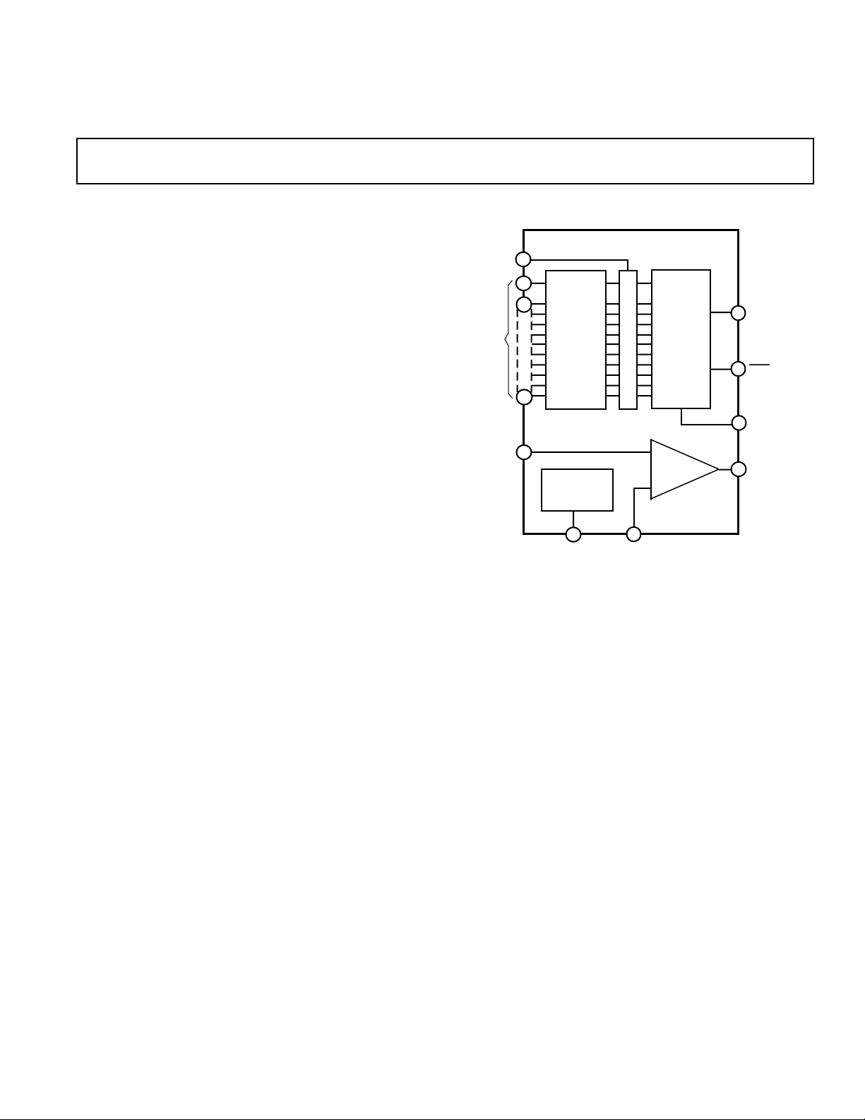
GENERAL DESCRIPTION
The AD9712B and AD9713B D/A converters are replacements
for the AD9712 and AD9713 units which offer improved ac and
dc performance. Like their predecessors, they are 12-bit, high
speed digital-to-analog converters fabricated in an advanced
oxide isolated bipolar process. The AD9712B is an ECLcompatible device featuring update rates of 100 MSPS minimum; the TTL-compatible AD9713B will update at 80 MSPS
minimum.
D/A Converters
AD9712B/AD9713B
FUNCTIONAL BLOCK DIAGRAM
REV. B
Information furnished by Analog Devices is believed to be accurate and
reliable. However, no responsibility is assumed by Analog Devices for its
use, nor for any infringements of patents or other rights of third parties
which may result from its use. No license is granted by implication or
otherwise under any patent or patent rights of Analog Devices.
Designed for direct digital synthesis, waveform reconstruction,
and high resolution imaging applications, both devices feature
low glitch impulse of 28 pV-s and fast settling times of 27 ns.
Both units are characterized for dynamic performance and have
excellent harmonic suppression.
The AD9712B and AD9713B are available in 28-pin plastic
DIPs and PLCCs, with an operating temperature range of
–25°C to +85°C. Both are also available for extended temperature ranges of –55°C to +125°C in cerdips and 28-pin LCC
packages.
One Technology Way, P.O. Box 9106, Norwood, MA 02062-9106, U.S.A.
Tel: 617/329-4700 Fax: 617/326-8703
Page 2

AD9712B/AD9713B–SPECIFICA TIONS
[–VS = –5.2 V; +VS = +5 V (AD9713B only); Reference Voltage = –1.2 V;
R
ELECTRICAL CHARACTERISTICS
= 7.5 kV; V
SET
AD9712B/AD9713B AD9712B/AD9713B AD9712B/AD9713B AD9712B/AD9713B
Test AN/AP BN/BP SE/SQ TE/TQ
Parameter (Conditions) Temp Level Min Typ Max Min Typ Max Min Typ Max Min Typ Max Units
RESOLUTION 12 12 12 12 Bits
DC ACCURACY
Differential Nonlinearity +25°C I –1.25 1.0 +1.25 –0.75 0.5 +0.75 –1.5 1.0 +1.5 –1.0 0.5 +1.0 LSB
Full VI –2.0 2.0 –1.5 1.5 –2.0 2.0 –1.5 1.5 LSB
Integral Nonlinearity +25°C I –1.5 1.0 1.5 –1.0 0.75 1.0 –1.75 1.5 1.75 –1.25 1.0 1.25 LSB
(“Best Fit” Straight Line) Full VI –2.0 2.0 –1.75 1.75 –2.0 2.0 –1.75 1.75 LSB
Test All Grades All Grades
Parameter (Conditions) Temp Level Min Typ Max Min Typ Max Units
INITIAL OFFSET ERROR
Zero-Scale Offset Error +25°C I 0.5 2.5 0.5 2.5 µA
Full VI 5.0 5.0 µA
+25°C I 1.0 5 1.0 5 %
Full-Scale Gain Error
1
Full VI 8 8 %
Offset Drift Coefficient +25°C V 0.01 0.01 µA/°C
REFERENCE/CONTROL AMP
Internal Reference Voltage +25°C I –1.14 –1.18 –1.22 –1.14 –1.18 –1.22 V
Full VI –1.12 –1.24 –1.12 –1.24 V
Internal Reference Voltage Drift Full V 50 50 ppm/°C
Internal Reference Output Current Full IV –50 +500 –50 +500 µA
Amplifier Input Impedance +25°C V 50 50 kΩ
Amplifier Bandwidth +25°C V 300 300 kHz
REFERENCE INPUT
Reference Input Impedance +25°CV 3 3 kΩ
Reference Multiplying Bandwidth
DYNAMIC PERFORMANCE
Full-Scale Output Current
2
3
4
+25°C V 40 40 MHz
+25°C V 20.48 20.48 mA
Output Compliance Range +25°C IV –1.2 +2 –1.2 +2 V
Output Resistance +25°C IV 2.0 2.5 3.0 2.0 2.5 3.0 kΩ
Output Capacitance +25°C V 15 15 pF
Output Update Rate
Output Settling Time (tST)
Output Propagation Delay (tPD)
Glitch Impulse
Output Rise Time
Output Fall Time
5
6
7
8
9
9
+25°C IV 100 110 80 100 MSPS
+25°C V 27 27 ns
+25°CV 6 7 ns
+25°C V 28 28 pV-s
+25°CV 2 2 ns
+25°CV 2 2 ns
DIGITAL INPUTS
Logic “1” Voltage Full VI –1.0 –0.8 2.0 V
Logic “0” Voltage Full VI –1.7 –1.5 0.8 V
Logic “1” Current Full VI 20 20 µA
Logic “0” Current Full VI 10 600 µA
Input Capacitance +25°CV 3 3 pF
Input Setup Time (tS)
Input Hold Time (tH)
10
11
+25°C IV 0.5 –0.3 0.5 –0.3 ns
Full IV 0.8 0.8 ns
+25°C IV 1.8 1.2 1.8 1.2 ns
Full IV 2.0 2.0 ns
Latch Pulse Width (t
) (LOW) +25°C IV 2.5 1.7 2.5 1.7 ns
LPW
(Transparent) Full 2.8 2.8 ns
AC LINEARITY
12
Spurious-Free Dynamic Range (SFDR)
1.23 MHz; 10 MSPS; 2 MHz Span +25 °C V 70 70 dB
5.055 MHz; 20 MSPS; 2 MHz Span +25°C V 72 72 dB
10.1 MHz; 50 MSPS; 2 MHz Span +25 °C V 68 68 dB
16 MHz; 40 MSPS; 10 MHz Span +25° C V 68 68 dB
= 0 V (virtual ground); unless otherwise noted]
OUT
AD9712B AD9713B
–2–
REV. B
Page 3

AD9712B/AD9713B
Test All Grades All Grades
AD9712B AD9713B
Parameter (Conditions) Temp Level Min Typ Max Min Typ Max Units
POWER SUPPLY
13
Positive Supply Current (+5.0 V) +25°CI 6 12 mA
Negative Supply Current (–5.2 V)
14
Full VI 14 mA
+25°C I 140 178 145 184 mA
Full VI 183 188 mA
Nominal Power Dissipation +25°C V 728 784 mW
Power Supply Rejection Radio (PSRR)15+25°C I 30 100 30 100 µA/V
NOTES
1
Measured as error in ratio of full-scale current to current through R
2
Full-scale variations among devices are higher when driving REFERENCE INPUT directly.
3
Frequency at which the gain is flat ±0.5 dB; RL = 50 Ω; 50% modulation at midscale.
4
Based on IFS = 128 (V
5
Data registered into DAC accurately at this rate; does not imply settling to 12-bit accuracy.
6
Measured as voltage settling at midscale transition to ±0.024%, RL = 50 Ω.
7
Measured as the time between the 50% point of the falling edge of LATCH ENABLE and the point where the output signal has left a 1 LSB error band
around its previous value.
8
Peak glitch impulse is measured as the largest area under a single positive or negative transient.
9
Measured with RL = 50 Ω and DAC operating in latched mode.
10
Data must remain stable for specified time prior to falling edge of LATCH ENABLE signal.
11
Data must remain stable for specified time after rising edge of LATCH ENABLE signal.
12
SFDR is defined as the difference in signal energy between the fundamental and worst case spurious frequencies in the output spectrum window, which is
centered at the fundamental frequency and covers the indicated span.
13
Supply voltages should remain stable within ±5% for normal operation.
14
108 mA typ on Digital –VS, 37 mA typ on Analog –VS.
15
Measured at ±5% of +VS (AD9713B only) and –VS (AD9712B or AD9713B) using external reference.
Specifications subject to change without notice.
ABSOLUTE MAXIMUM RATINGS
) when using internal amplifier.
REF/RSET
1
Positive Supply Voltage (+VS) (AD9713B Only) . . . . . . . +6 V
Negative Supply Voltage (–V
) . . . . . . . . . . . . . . . . . . . . . –7 V
S
Analog-to-Digital Ground Voltage Differential . . . . . . . . 0.5 V
Digital Input Voltages (D
, LATCH ENABLE)
1–D12
AD9712B . . . . . . . . . . . . . . . . . . . . . . . . . . . . . . . 0 V to –V
AD9713B . . . . . . . . . . . . . . . . . . . . . . . . . . . . .–0.5 V to +V
Internal Reference Output Current . . . . . . . . . . . . . . . .500 µA
Control Amplifier Input Voltage Range . . . . . . . . . 0 V to –4 V
Control Amplifier Output Current . . . . . . . . . . . . . . . ±2.5 mA
Reference Input Voltage Range (V
) . . . . . . . . . . . 0 V to –V
REF
Analog Output Current . . . . . . . . . . . . . . . . . . . . . . . . . 30 mA
Operating Temperature Range
AD9712B/AD9713BAN/AP/BN/BP . . . . . . .–25°C to +85°C
AD9712B/AD9713BSE/SQ/TE/TQ . . . . . .–55°C to +125°C
Maximum Junction Temperature
2
AD9712B/AD9713BAN/AP/BN/BP . . . . . . . . . . . . . +150°C
AD9712B/AD9713BSE/SQ/TE/TQ . . . . . . . . . . . . . +175°C
Lead Temperature (Soldering, 10 sec) . . . . . . . . . . . . . +300°C
(160 µA nominal); ratio is nominally 128.
SET
Model Range Description Option
AD9712BAN –25°C to +85°C 28-Pin PDIP N-28
AD9712BBN –25°C to +85°C 28-Pin PDIP N-28
S
AD9712BAP –25°C to +85°C 28-Pin PLCC P-28A
S
AD9712BBP –25°C to +85°C 28-Pin PLCC P-28A
AD9712BSQ/883B –55°C to +125°C 28-Pin Cerdip Q-28
AD9712BSE/883B –55°C to +125°C 28-Pin LCC E-28A
AD9712BTQ/883B –55°C to +125°C 28-Pin Cerdip Q-28
S
AD9712BTE/883B –55°C to +125°C 28-Pin LCC E-28A
AD9713BAN –25°C to +85°C 28-Pin PDIP N-28
AD9713BBN –25°C to +85°C 28-Pin PDIP N-28
AD9713BAP –25°C to +85°C 28-Pin PLCC P-28A
AD9713BBP –25°C to +85°C 28-Pin PLCC P-28A
AD9713BSQ/883B –55°C to +125°C 28-Pin Cerdip Q-28
AD9713BSE/883B –55°C to +125°C 28-Pin LCC E-28A
AD9713BTQ/883B –55°C to +125°C 28-Pin Cerdip Q-28
AD9713BTE/883B –55°C to +125°C 28-Pin LCC E-28A
ORDERING GUIDE
Temperature Package Package
Storage Temperature Range . . . . . . . . . . . . .–65°C to +150°C
NOTES
1
Absolute maximum ratings are limiting values to be applied individually, and
beyond which the serviceability of the circuit may be impaired. Functional
operability is not necessarily implied. Exposure to absolute maximum rating
conditions for an extended period of time may affect device reliability.
2
Typical thermal impedances with parts soldered in place: 28-pin plastic DIP:
θJA = 37°C/W, θJC = 10°C/W; 28-pin PLCC: θJA = 44°C/W, θJC = 14°C/W;
Cerdip: θJA = 32°C/W, θJC = 10°C/W; LCC: θJA = 41°C/W, θJC = 13°C/W. No air
flow.
EXPLANATION OF TEST LEVELS
Test Level
I – 100% production tested.
II – 100% production tested at +25°C, and sample tested at
specified temperatures.
III – Sample tested only.
IV – Parameter is guaranteed by design and characterization
testing.
V – Parameter is a typical value only.
VI – All devices are 100% tested at +25°C. 100% production
tested at temperature extremes for extended tempera-
ture devices; sample tested at temperature extremes for
commercial/industrial devices.
REV. B
–3–
Page 4
AD9712B/AD9713B
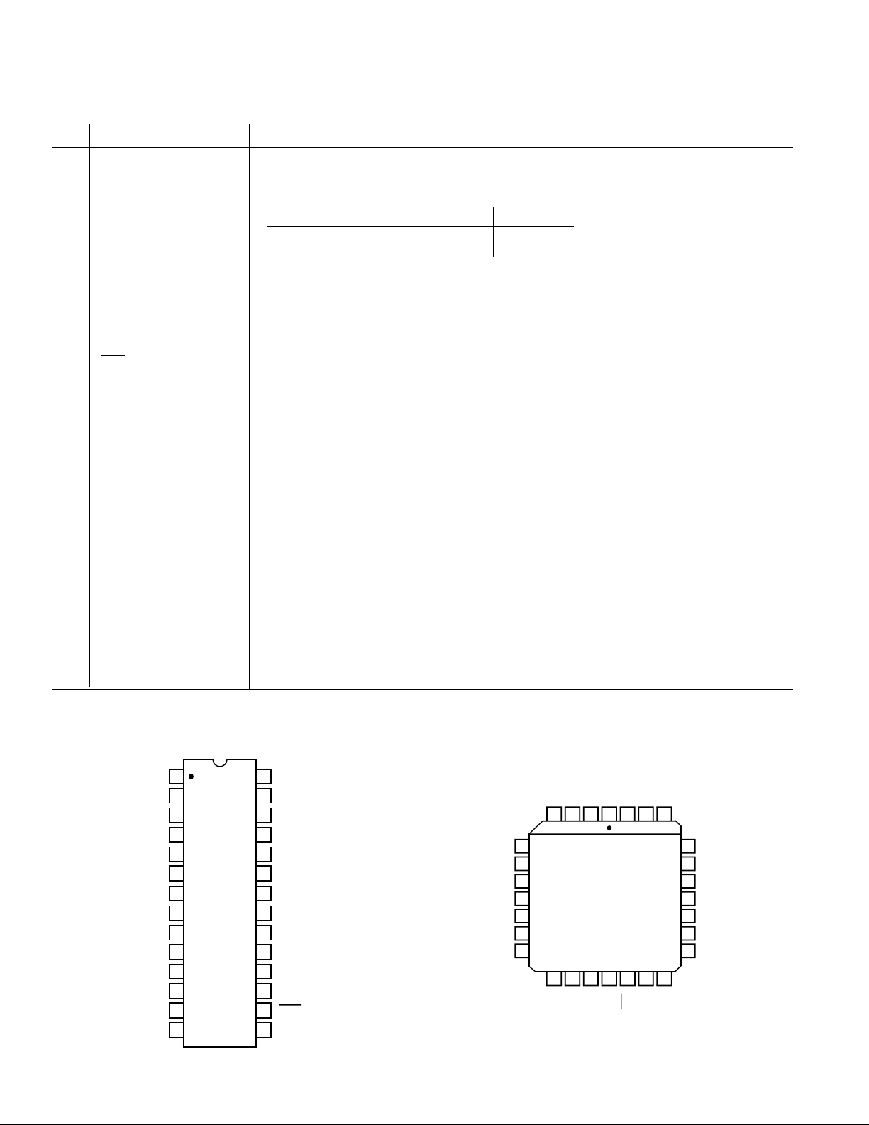
Pin # Name Function
PIN DESCRIPTIONS
1–10 D2–D
11 D
(LSB) Least Significant Bit (LSB) of digital input word.
12
11
Ten bits of twelve-bit digital input word.
Input Coding vs. Current Output
Input Code D
1–D12
I
(mA) I
OUT
OUT
(mA)
1111111111 –20.475 0
0000000000 0 –20.475
12 DIGITAL –V
S
One of two negative digital supply pins; nominally –5.2 V.
13 ANALOG RETURN Analog ground return. This point and the reference side of the DAC load resistors should be
connected to the same potential (nominally ground).
14 I
OUT
15 ANALOG –V
16 I
OUT
S
Analog current output; full-scale output occurs with digital inputs at all “1.”
One of two negative analog supply pins; nominally –5.2 V.
Complementary analog current output; zero scale output occurs with digital inputs at all “1.”
17 REFERENCE IN Normally connected to CONTROL AMP OUT (Pin 18). Direct line to DAC current source
network. Voltage changes at this point have a direct effect on the full-scale output value of
unit. Full-scale current output = 128 (Reference voltage/R
) when using internal amplifier.
SET
18 CONTROL AMP OUT Normally connected to REFERENCE INPUT (Pin 17). Output of internal control amplifier,
which provides a temperature-compensated drive level to the current switch network.
19 CONTROL AMP IN Normally connected to REFERENCE OUT (Pin 20) if not connected to external reference.
20 REFERENCE OUT Normally connected to CONTROL AMP IN (Pin 19). Internal voltage reference, nominally
–1.18 V.
21 DIGITAL –V
S
One of two negative digital supply pins; nominally –5.2 V.
22 REFERENCE GROUND Ground return for the internal voltage reference and amplifier.
23 DIGITAL +V
S
Positive digital supply pin, used only on the AD9713B; nominally +5 V. No connection to this
pin on AD9712B.
24 R
SET
25 ANALOG –V
S
Connection for external resistance reference. Full-scale current out = 128 (Reference voltage/
R
) when using internal amplifier. Nominally 7.5 kΩ.
SET
One of two negative analog supply pins; nominally –5.2 V.
26 LATCH ENABLE Transparent latch control line. Register is transparent when LATCH ENABLE is LOW.
27 DIGITAL GROUND Digital ground return.
28 D1 (MSB) Most Significant Bit (MSB) of digital input word.
D
D
D12 (LSB)
DIGITAL –V
ANALOG RETURN
I
OUT
D
D
D
D
D
D
D
D
10
11
2
3
4
5
6
7
8
9
S
1
2
3
4
5
AD9712B
6
AD9713B
7
8
(Not to Scale)
9
10
11
12
13
14
DIP
TOP VIEW
D1 (MSB0)
28
27
DIGITAL GROUND
26
LATCH ENABLE
25
ANALOG –V
R
24
SET
23
DIGITAL +V
REFERENCE GROUND
22
21
DIGITAL –V
20
REFERENCE OUT
CONTROL AMP IN
19
18
CONTROL AMP OUT
17
REFERENCE IN
I
16
OUT
15
ANALOG –V
PIN CONFIGURATIONS
S
S
S
S
–4–
D
D
D (LSB)
12
PLCC/LCC
4
5
D
4
5
D
6
6
D
7
7
D
8
8
D
9
9
10
10
11
11
12
13 141516 17 18
S
DIGITAL –V
3
D
D
D
1
23
AD9712B
AD9713B
TOP VIEW
(Not to Scale)
S
OUT
I
RETURN
ANALOG
ANALOG –V
2
1
D (MSB)
28 27
OUT
I
ENABLE
LATCH
GROUND
DIGITAL
26
25
24
23
22
21
20
19
AMP OUT
CONTROL
REFERENCE IN
ANALOG –V
R
SET
DIGITAL +V
REFERENCE
GROUND
DIGITAL –V
REFERENCE
OUT
CONTROL
AMP IN
S
S
S
REV. B
Page 5

AD9712B/AD9713B
DIE LAYOUT AND METALIZATION INFORMATION
Die Dimensions . . . . . . . . . . . . . . . . . 220 × 196 × 15 (± 2) mils
Pad Dimensions . . . . . . . . . . . . . . . . . . . . . . . . . . . . .4 × 4 mils
Metalization . . . . . . . . . . . . . . . . . . . . . . . . . . . . . . . Aluminum
Backing . . . . . . . . . . . . . . . . . . . . . . . . . . . . . . . . . . . . . . None
Substrate Potential . . . . . . . . . . . . . . . . . . . . . . . . . . . . . . . –V
S
Passivation . . . . . . . . . . . . . . . . . . . . . . . . . . . . . . . . . . .Nitride
THEORY AND APPLICATIONS
The AD9712B and AD9713B high speed digital-to-analog
converters utilize Most Significant Bit (MSB) decoding and
segmentation techniques to reduce glitch impulse and maintain 12-bit linearity without trimming.
As shown in the functional block diagram, the design is based
on four main subsections: the Decoder/Driver circuits, the
Transparent Latches, the Switch Network, and the Control Amplifier. An internal bandgap reference is also included to allow
operation with a minimum of external components.
Digital Inputs/Timing
The AD9712B employs single-ended ECL-compatible inputs
for data inputs D
and LATCH ENABLE. The internal
1–D12
ECL midpoint reference is designed to match 10K ECL device
thresholds. On the AD9713B, a TTL translator is added at each
input; with this exception, the AD9712B and AD9713B are
identical.
In the Decoder/Driver section, the four MSBs (D
1–D4
) are
decoded to 15 “thermometer code” lines. An equalizing delay is
included for the eight Least Significant Bits (LSBs) and
LATCH ENABLE. This delay minimizes data skew, and data
setup and hold times at the latch inputs; this is important when
operating the latches in the transparent mode. Without the
delay, skew caused by the decoding circuits would degrade
glitch impulse.
The latches operate in their transparent mode when LATCH
ENABLE (Pin 26) is at logic level “0.” The latches should be
used to synchronize data to the current switches by applying a
narrow LATCH ENABLE pulse with proper data setup and
hold times as shown in the Timing Diagram. An external latch
at each data input, clocked out of phase with the Latch Enable,
operates the AD9712B/AD9713B in a master slave (edgetriggered) mode. This is the optimum way to operate the DAC
because data is always stable at the DAC input. An external
latch eases timing constraints when using the converter.
Although the AD9712B/AD9713B chip is designed to provide
isolation from digital inputs to the outputs, some coupling of
digital transitions is inevitable, especially with TTL or CMOS
inputs applied to the AD9713B. Digital feedthrough can be reduced by forming a low-pass filter using a (200 Ω) series resistor
in series with the capacitance of each digital input; this rolls off
the slew rate of the digital inputs.
References
As shown in the functional block diagram, the internal bandgap
reference, control amplifier, and reference input are pinned out
for maximum user flexibility when setting the reference.
When using the internal reference, REFERENCE OUT (Pin 20)
should be connected to CONTROL AMP IN (Pin 19). CONTROL AMP OUT (Pin 18) should be connected to REFERENCE IN (Pin 17) through a 20 Ω resistor. A 0.1 µF ceramic
capacitor from Pin 17 to –V
(Pin 15) improves settling by
S
decoupling switching noise from the current sink base line. A
reference current cell provides feedback to the control amp by
sinking current through R
(Pin 24).
SET
REV. B
LATCH ENABLE
DATA INPUTS
OUTPUT
t
LPW
t
S
VALID DATA
t
PD
t
H
t
– LATCH PULSE WIDTH
LPW
t
– INPUT SETUP TIME
S
LATCH
ENABLE
OUTPUT
ERROR
t
t
– INPUT HOLD TIME
H
t
– OUTPUT SETTLING TIME
ST
t
– OUTPUT PROPAGATION DELAY
PD
ERROR
BAND
t
PD
ST
Timing Diagram
–5–
Page 6

AD9712B/AD9713B
Full-scale output current is determined by CONTROL AMP
IN and R
according to the equation:
SET
(FS) = (CONTROL AMP IN/R
I
OUT
SET
) × 128
The internal reference is nominally –1.18 V with a tolerance of
±3.5% and typical drift over temperature of 50 ppm/°C. If
greater accuracy or better temperature stability is required, an
external reference can be utilized. The AD589 reference shown
in Figure 1 features ±10 ppm/°C drift over temperatures from
0°C to +70°C.
AD9712B
19
AD9713B
CONTROL
AMP IN
AD589
+
–
R
1
~
11k
–
–V
S
Figure 1. Use of AD589 as External Reference
Two modes of multiplying operation are possible with the
AD9712B/AD9713B. Signals with small signal bandwidths up
to 300 kHz and input swings of 100 mV, or dc signals from
–0.6 V to –1.2 V can be applied to the CONTROL AMP input
as shown in Figure 2. Because the control amplifier is internally
compensated, the 0.1 µF capacitor at Pin 17 can be reduced to
0.01 µF to maximize the multiplying bandwidth. However, it
should be noted that settling time for changes to the digital inputs will be degraded.
R
SET
24
R
SET
–0.6V TO –1.2V
300 kHz MAX
R
T
19
CONTROL
AMP IN
AD9712B
AD9713B
The REFERENCE IN pin can also be driven directly for wider
bandwidth multiplying operation. The analog signal for this
mode of operation must have a signal swing in the range of
–3.75 V to –4.25 V. This can be implemented by capacitively
coupling into REFERENCE IN a signal with a dc bias of –3.75 V
to –4.25 V, as shown in Figure 3; or by driving REFERENCE
IN with a low impedance op amp whose signal swing is limited
to the stated range.
Outputs
As indicated earlier, D1–D4 (four MSBs) are decoded and drive
15 discrete current sinks. D5 and D6 are binarily weighted; and
D
are applied to the R-2R network. This segmented archi-
7–D12
tecture reduces frequency domain errors due to glitch impulse.
AD9712B
AD9713B
REFERENCE
IN
17
~
–4V
–
–V
S
–V
S
Figure 3. Wideband Multiplying Circuit
The Switch Network provides complementary current outputs
I
OUT
and I
. These current outputs are based on statistical
OUT
current source matching which provides 12-bit linearity without
trim. Current is steered to either I
OUT
or I
in proportion to
OUT
the digital input code. The sum of the two currents is always
equal to the full-scale output current minus one LSB.
The current output can be converted to a voltage by resistive
loading as shown in Figure 4. Both I
OUT
and I
should be
OUT
loaded equally for best overall performance. The voltage which
is developed is the product of the output current and the value
of the load resistor.
CONTROL
18
18
AMP OUT
REFERENCE
17
IN
Figure 2. Low Frequency Multiplying Circuit
–6–
REV. B
Page 7

0.01µF0.1µF
–5.2V
0.01µF
DIGITAL –V
28
D (MSB)
1
1
D
2
2
D
3
3
D
4
4
D
5
5
D
6
6
D
7
7
D
8
8
D
9
9
D
10
10
D
11
11
D (LSB)
12
26
LATCH ENABLE
ANALOG
RETURN
13
12,21
S
REFERENCE
GROUND
22 27
15,25
ANALOG –V
REFERENCE
CONTROL
AMP OUT
REFERENCE
OUT
CONTROL
AMP IN
R
SET
I
OUT
AD9712B
AD9713B
I
OUT
DIGITAL
GROUND
S
IN
0.1µF
17
20Ω
18
20
19
24
16
R
L
V
=
OUT
x R
I
R
FS
L
14
L
SYSTEM
GROUND
ECL
DRIVE
LOGIC
0.1µF
Figure 4. Typical Resistive Load Connection
An operational amplifier can also be used to perform the I to V
conversion of the DAC output. Figure 5 shows an example of a
circuit which uses the AD9617, a high speed, current feedback
amplifier.
10k
20
REF
OUT
AD9712B
AD9713B
10k
19
CONTROL
AMP IN
I
OUT
I
OUT
–
1/2 AD708
+
I
FS
14
16
12.5
200
R
1
100
I
OS
R
2
25
R
FF
25
R
L
400
R
FB
–
AD9617
+
V
OUT
±2.048V
+
1/2 AD708
–
Figure 5. I/VConversion Using Current Feedback
AD9712B/AD9713B
DAC current across feedback resistor RFB determines the
AD9617 output swing. A current divider formed by R
limits the current used in the I-to-V conversion, and provides an
output voltage swing within the specifications of the AD9617.
Current through R
AD9617. Adjusting the value of R
provides dc offset at the output of the
2
adjusts the value of offset
1
current. This offset current is based on the reference of the
AD9712B/AD9713B, to avoid coupling noise into the output
signal.
The resistor values in Figure 5 provide a 4.096 V swing, centered at ground, at the output of the AD9617 amplifier.
Power and Grounding
Maintaining low noise on power supplies and ground is critical
for obtaining optimum results with the AD9712B or AD9713B.
DACs are most often used in circuits which are predominantly
digital. To preserve 12-bit performance, especially at conversion
speeds up to 100 MSPS, special precautions are necessary for
power supplies and grounding.
Ideally, the DAC should have a separate analog ground plane.
All ground pins of the DAC, as well as reference and analog
output components, should be tied directly to this analog
ground plane. The DAC’s ground plane should be connected to
the system ground plane at a single point.
Ferrite beads such as the Stackpole 57-1392 or Amidon
FB-43B-101, along with high frequency, low-inductance decoupling capacitors, should be used for the supply connections to
isolate digital switching currents from the DAC supply pins.
Separate isolation networks for the digital and analog supply
connections will further reduce supply noise coupling to the
output.
Molded socket assemblies should be avoided even when
prototyping circuits with the AD9712B or AD9713B. When
the DAC cannot be directly soldered into the board, individual
pin sockets such as AMP #6-330808-0 (knock-out end), or
#60330808-3 (open end) should be used. These have much
less effect on inter-lead capacitance than do molded assemblies.
DDS Applications
Numerically controlled oscillators (NCOs) are digital devices
which generate samples of a sine wave. When the NCO is combined with a high performance D/A converter (DAC), the combination system is referred to as a Direct Digital Synthesizer
(DDS).
The digital samples generated by the NCO are reconstructed by
the DAC and the resulting sine wave is usable in any system
which requires a stable, spectrally pure, frequency-agile reference. The DAC is often the limiting factor in DDS applications,
since it is the only analog function in the circuit. The AD9712B/
AD9713B D/A converters offer the highest level of performance
available for DDS applications.
DC linearity errors of a DAC are the dominant effect in lowfrequency applications and can affect both noise and harmonic
content in the output waveform. Differential Nonlinearity
(DNL) errors determine the quantization error between adjacent codes, while Integral Nonlinearity (INL) is a measure of
how closely the overall transfer function of the DAC compares
with an ideal device. Together, these errors establish the limits
of phase and amplitude accuracy in the output waveform.
and R
L
FF
REV. B
–7–
Page 8

AD9712B/AD9713B
1ns/div
90
100
10
0%
200mV/div
SYSTEM
CLOCK
NUMERICALLY-CONTROLLED OSCILLATOR
WORD
32
PHASE
ACCUMULATOR
14
PHASE-TO-AMPLITUDE
CONVERSION
TUNING
Figure 6. Direct Digital Synthesizer Block Diagram
When the analog frequency (fA) is exactly fC/N and N is an even
integer, the DDS continually uses a small subset of the available
DAC codes. The DNL of the converter is effectively the DNL
error of the codes used, and is typically worse than the error
measured against all available DAC codes. This increase in
DNL is translated into higher harmonic and noise levels at the
output.
Glitch impulse, often considered a figure of merit in DDS applications, is simply the initial transient response of the DAC as it
moves between two output levels. This nonlinearity is commonly associated with external data skew, but this effect is minimized by using the on-board registers of the AD9712B/AD9713B
converters (see Digital Inputs/Timing section). The majority of
the glitch impulse, shown below, is produced as the current in
the R-2R ladder network settles, and is fairly constant over the
full-scale range of the DAC. The fast transients which form the
glitch impulse appear as high-frequency spurs in the output
spectrum.
While it is difficult to predict the effects of glitch on the output
waveform, slew rate limitations translate directly into harmonics.
This makes slew rate the dominant effect in ac linearity of the
DAC. Applications in which the ratio of analog frequency (f
to clock frequency (f
) is relatively high will benefit from the
C
)
A
high slew rate and low output capacitance of the AD9712B/
AD9713B devices.
Another concern in DDS applications is the presence of aliased
harmonics in the output spectrum. Aliased harmonics appear as
spurs in the output spectrum at frequencies which are determined by:
MfA ± Nf
C
where M and N are integers.
The effects of these spurs are most easily observed in applica-
tions where f
is nearly equal to an integer fraction of the clock
A
rate. This condition causes the aliased harmonics to fold near
the fundamental output frequency (see Performance Curves.)
D
1
OUTPUT
SINE DATA
12
5mV/div
TTL
REGISTER
100
90
10
0%
12
5ns/div
D
12
Figure 7. AD9712B/AD9713B Glitch Impulse
Figure 8. Rise and Fall Characteristics
LATCH
ENABLE
AD9712B
AD9713B
D/A CONVERTER
–8–
REV. B
Page 9

AD9712B/AD9713B
Figure 9a.
Figure 9b.
Figure 9d.
Figure 9e.
REV. B
Figure 9c.
Figure 9f.
Figure 9. Typical Spectral Performance
–9–
Page 10

AD9712B/AD9713B
Figure 10a.
Figure 10b.
Figure 10c.
Figure 10d.
Figure 10e.
Figure 10. Typical Spectral Performance
–10–
REV. B
Page 11

+5V
TTL
IN
TTL Input Buffer
10 kΩ
ECL
IN
–5.2 V
ECL Input Buffer
ECL V
MID
AD9712B/AD9713B
CONTROL
Control Amplifier Input
AMP IN
19
–5.2 V
±
REFERENCE
CONTROL
OUT
AMP IN
20
19
Full-Scale Current Control Loop
R
D
12
2R 2R 2R
R
D
R
11
D
10
24
R
SET
+
R
D
9
CONTROL
AMP
–
R
18
CONTROL
AMP OUT
2R
RR
D
8
R-2R DAC (for 6 LSBs)
D
7
17
REFERENCE
IN
2R
D1D
–
V
BIAS
–5.2 V
–5.2 V
18
CONTROL
AMP OUT
Control Amp Output
ANALOG
13
RETURN
14
I
OUT
or
16
I
6
OUT
REFERENCE
IN
17
–5.2 V
138 CURRENT SOURCES
Reference Input
REV. B
2.5kΩ
16pF
I
OUT
14
–V
S
Output Circuit
I
OUT
16
16pF
ANALOG
RETURN
13
2.5kΩ
Figure 11. Equivalent Circuits
–11–
–5.2 V
Reference Output
REFERENCE
20
OUT
Page 12

AD9712B/AD9713B
PIN 1
IDENTIFIER
4
26
5
11
25
19
12
18
0.430 (10.92)
0.390 (9.91)
0.050
(1.27)
BSC
0.021 (0.53)
0.013 (0.33)
0.032 (0.81)
0.026 (0.66)
0.456 (11.58)
0.450 (11.43)
0.495 (12.57)
0.485 (12.32)
0.456 (11.58)
0.450 (11.43)
0.048 (1.21)
0.042 (1.07)
0.048 (1.21)
0.042 (1.07)
0.048 (1.21)
0.042 (1.07)
0.495 (12.57)
0.485 (12.32)
0.025 (0.63)
0.015 (0.38)
0.040 (1.01)
0.025 (0.64)
0.110 (2.79)
0.085 (2.16)
0.180 (4.57)
0.165 (4.19)
OUTLINE DIMENSIONS
Dimensions shown in inches and (mm).
0.250 (6.35)
MAX
0.22
(5.59)
MAX
28
1
0.022 (0.558)
0.014 (0.356)
28
1
GLASS SEALANT
0.026 (0.660)
0.014 (0.356)
28-Pin Plastic DIP (Suffix N)
15
0.550 (13.97)
0.530 (13.46)
14
1.565 (39.70)
1.380 (35.10)
0.100 (2.54)
BSC
0.70 (1.77)
MAX
0.060 (1.52)
0.015 (0.38)
0.140
(3.56)
MIN
28-Pin Cerdip (Suffix Q)
1.490 (37.84) MAX
15
0.610 (15.49)
0.500 (12.70)
14
0.110 (2.79)
0.098 (2.45)
0.07 (1.78)
0.03 (0.76)
0.125
(3.175)
MIN
0.625 (15.8)
0.600 (15.24)
0.015 (0.381)
0.008 (0.204)
0.620 (15.74)
0.590 (14.93)
0.018 (0.45)
0.008 (0.20)
15
0
28-Pin Plastic Leaded Chip Carrier (Suffix P)
28-Pin LCC Package (Suffix E)
0.055 (1.40)
0.045 (1.14)
27 28
26
25
24
23
22
21
20
19
123
BOTTOM VIEW
0.458 (11.63)
0.442 (11.23)
1314151617
0.075
(1.91)
REF
4
1218
5
6
7
8
9
10
11
0.028 (0.71)
0.022 (0.56)
0.050 (1.27)
0.100 (2.54)
0.064 (1.63)
C1635–24–3/92
PRINTED IN U.S.A.
–12–
REV. B
 Loading...