

Page 1
250 MSPS Video
a
FEATURES
250 MSPS Update Rate
Low Glitch Impulse
Complete Composite Functions
Internal Voltage Reference
Single –5.2 V Supply
APPLICATIONS
Raster Scan Displays
Color Graphics
Automated Test Equipment
TV Video Reconstruction
GENERAL DESCRIPTION
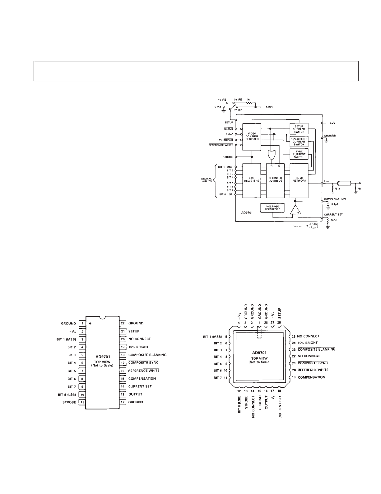
The AD9701 is a high speed, 8-bit digital-to-analog converter
with fully integrated composite video functions. High speed
ECL input registers provide synchronous operation of data and
control functions up to 250 MSPS.
The AD9701 incorporates onboard control functions including
horizontal sync, blanking, reference white level and a 10%
bright signal for highlighting. The setup level is also adjustable
from 0 IRE units to 20 IRE units through the control pin. An
internal voltage reference allows the AD9701 to operate as a
stand-alone video reconstruction DAC.
The AD9701 is available as an industrial temperature range
device, –25°C to +85°C, and as an extended temperature range
Digital-to-Analog Converter
AD9701
FUNCTIONAL BLOCK DIAGRAM
device, –55°C to +125°C. Both grades of the AD9701 are packaged in a 22-pin ceramic DIP with the extended temperature
device also available in a 28-pin LCC package.
PIN CONFIGURATIONS
REV. A
Information furnished by Analog Devices is believed to be accurate and
reliable. However, no responsibility is assumed by Analog Devices for its
use, nor for any infringements of patents or other rights of third parties
which may result from its use. No license is granted by implication or
otherwise under any patent or patent rights of Analog Devices.
One Technology Way, P.O. Box 9106, Norwood, MA 02062-9106, U.S.A.
Tel: 617/329-4700 World Wide Web Site: http://www.analog.com
Fax: 617/326-8703 © Analog Devices, Inc., 1996
Page 2
AD9701–SPECIFICATIONS
ABSOLUTE MAXIMUM RATINGS
Supply Voltage (–VS) . . . . . . . . . . . . . . . . . . . . . . . . . . . . –7 V
Digital Input Voltages (Including STROBE, SYNC,
BLANKING, 10% BRIGHT and REFERENCE
WHITE) . . . . . . . . . . . . . . . . . . . . . . . . . . . . . . .0 V to –V
Analog Output Current . . . . . . . . . . . . . . . . . . . . . . . . 37 mA
Power Dissipation (+25°C Free Air)
ELECTRICAL CHARACTERISTICS
1
2
. . . . . . . . . . . . 780 mW
(Supply Voltages = –5.2 V; RL = 37.5 V; Setup = 0 V, unless otherwise noted)
Operating Temperature Range
AD9701BQ . . . . . . . . . . . . . . . . . . . . . . . . –25°C to +85°C
AD9701SQ/SE . . . . . . . . . . . . . . . . . . . . . –55°C to +125°C
Storage Temperature Range . . . . . . . . . . . . –65°C to +150°C
Junction Temperature . . . . . . . . . . . . . . . . . . . . . . . . +175°C
S
Lead Soldering Temperature (10 sec) . . . . . . . . . . . . +300°C
AD9701BQ AD9701SQ/SE
Parameter Temp Min Typ Max Min Typ Max Units
RESOLUTION 8 8 Bits
DC ACCURACY
Differential Linearity +25°C 0.25 0.5 0.25 0.5 LSB
Full 1.0 1.0 LSB
Integral Linearity +25°C 0.25 0.5 0.25 0.5 LSB
Full 1.0 1.0 LSB
Monotonicity Full Guaranteed Guaranteed
INITIAL OFFSET ERROR
Zero-Scale Offset Error
3
4
+25°C 0.05 0.9 0.05 0.9 mV
Full 0.9 0.9 mV
Zero-Scale Offset Drift Coefficient Full 2 2 µV/°C
Full-Scale Drift Coefficient Full 50 50 µV/°C
ANALOG OUTPUT
Voltage Output
10% Bright
Reference White Full –67.45 –71 –74.55 –67.45 –71 –74.55 mV
Blanking (Setup = 0 IRE)
Sync (Setup = 0 IRE)
Current Output
10% Bright
Reference White Full –1.805 –1.9 –1.996 –1.805 –1.9 –1.995 mA
Blanking (Setup = 0 IRE)
Sync (Setup = 0 IRE)
5
6
7
8
5
6
7
8
Full –0.9 0 –0.9 0 mV
Full –698.55 –708.5 –718.45 –698.55 –708.5 –718.45 mV
Full –979.25 –993.5 –1007.75 –979.25 –993.5 –1007.75 mV
Full –0.024 0 –0.024 0 mA
Full –18.63 –18.9 –19.16 –18.63 –18.9 –19.16 mA
Full –26.11 –26.5 –26.87 –26.11 –26.5 –26.87 mA
Output Compliance Range Full –1.6; +0.1 –1.6; +0.1 V
Output Resistance +25°C 640 800 640 800 Ω
DYNAMIC PERFORMANCE
Update Rate +25°C 225 250 225 250 MSPS
Output Propagation Delay
Output Settling Time
9
10
+25°C56 56ns
Current +25°C8 8 ns
Voltage +25°C12 12 ns
Output Slew Rate
Output Rise Time
Output Fall Time
11
11
11
+25°C 255 300 255 300 V/µs
+25°C 1.7 2.0 1.7 2.0 ns
+25°C 1.7 2.0 1.7 2.0 ns
Glitch Impulse +25°C 60 70 60 70 pV-s
SETUP CONTROL
12
Setup Level (Grounded) Full 0 0 IRE
Setup Level (Open) Full 7.5 7.5 IRE
Setup Level
(Tied to –5.2 V with 1 kΩ) Full 10 10 IRE
Setup Level (–5.2 V) Full 20 20 IRE
DIGITAL INPUTS
Logic “1” Voltage Full –1.1 –1.1 V
Logic “0” Voltage Full –1.5 –1.5 V
Logic “1” Current Full 100 100 µA
Logic “0” Current Full 15 15 µA
Input Capacitance +25°C 4 5.5 4 5.5 pF
Data Setup Time +25°C 0.1 0.1 ns
Data Hold Time +25°C 1.4 1.4 ns
–2–
REV. A
Page 3

AD9701
AD9701
AD9701BQ AD9701SQ/SE
Parameter Temp Min Typ Max Min Typ Max Units
POWER SUPPLY
13
Supply Current (–5.2 V) +25°C 140 160 140 160 mA
Full 160 160 mA
Nominal Power Dissipation +25°C 728 728 mW
Power Supply Rejection Ratio
NOTES
1
Absolute maximum ratings are limiting values to be applied individually, and beyond which serviceability of the circuit may be impaired. Functional operability under
any of these conditions is not necessarily implied. Exposure to absolute maximum rating conditions for extended periods may affect device reliability.
2
Typical thermal impedance . . .
22-Pin Ceramic θJA = 64°C/W; θJC = 16°C/W
28-Pin Ceramic LCC θJA = 70°C/W θJC = 21°C/W
3
SYNC, BLANKING, and REFERENCE WHITE are inactive (Logic “1”). I
4
All bits at logic HIGH.
5
All values are relative to full-scale output after being normalized to nominal value. Typical variation in full-scale output from device to device can reach ±10%, for a
fixed R
6
The effect of 10% BRIGHT algebraically adds to the output waveform.
7
The output level with BLANKING active (Logic “0”) is determined by the setup control level.
8
In normal operation, the BLANKING input is activated (Logic “0”) prior to or in conjunction with the SYNC input. The effect of the SYNC output is relative to the
setup level.
9
Measured from edge of STROBE to 50% transition point of the output signal.
10
11
12
13
14
Specifications subject to change without notice.
resistor.
SET
Measured with full-scale change in output level, from the 10% transition level to within ±0.2% of the final output value.
Measured from 10% to 90% transition point for full-scale step output.
An IRE unit is 1% of the Grey Scale (GS range) with a 0 IRE setup level.
Supply Voltage should remain stable within ±5% for normal operation.
Measured at ±5% of –VS.
14
Full 3 6 3 6 mV/V
≈ 1.26 V/R
SET
SET
.
DIGITAL INPUTS VS. ANALOG OUTPUT
Bit Bit Bit Bit Bit Bit Bit Bit 10% Ref. Comp. Analog
12345678 Bright White Blanking Sync Output (mV)
11111111 0 1 1 1 0
11111111 1 1 1 1 –71
10000000 0 1 1 1 –320
00000000 0 1 1 1 –637.5
00000000 1 1 1 1 –708.5
XXXXXXXX 0 0 1 1 0
XXXXXXXX 1 0 1 1 –71
XXXXXXXX 0 1 0 1 –637.50
XXXXXXXX 0 1 0 1 –690.75
XXXXXXXX 0 1 0 1 –708.50
XXXXXXXX 0 1 0 1 –779.50
XXXXXXXX 0 1 0 0 –922.50
XXXXXXXX 0 1 0 0 –975.75
XXXXXXXX 0 1 0 0 –993.50
XXXXXXXX 0 1 0 0 –1064.50
XXXXXXXX 1 1 0 0 –993.50
XXXXXXXX 1 1 0 0 –1046.75
XXXXXXXX 1 1 0 0 –1064.50
XXXXXXXX 1 1 0 0 –1135.50
NOTES
1
Setup (Pin 21) grounded (0 IRE units).
2
Setup (Pin 21) open (7.5 IRE units).
3
Setup (Pin 21) to –5.2 V through 1 k (0 IRE units).
4
Setup (Pin 21) to –5.2 V (20 IRE units).
1
2
3
4
1
2
3
4
1
2
3
4
REV. A
ORDERING GUIDE
Temperature Package
Device Range Description Option*
AD9701BQ –25°C to +85°C 22-Pin DIP, Industrial Temperature Q-22
AD9701SE –55°C to +125°C 28-Pin LCC, Extended Temperature E-28A
AD9701SQ –55°C to +125°C 22-Pin DIP, Extended Temperature Q-22
*E = Leadless Ceramic Chip Carrier; Q = Cerdip.
–3–
Page 4

AD9701
FUNCTIONAL DESCRIPTION
Pin Name Description
GROUND One of three ground returns. All grounds should be connected together near the AD9701.
–V
S
BIT 1 (MSB) One of eight digital input bits. BIT 1 (MSB) is the most-significant-bit of the digital input word.
BIT 2–BIT 7 One of eight digital input bits.
BIT 8 (LSB) One of eight digital input bits. BIT 8 (LSB) is the least-significant-bit of the digital input word.
STROBE Data and control register strobe input. STROBE is leading edge triggered.
GROUND One of three ground returns. All grounds should be connected together near the AD9701.
SETUP The SETUP input determines the position of the blanking level relative to the “reference black”
10% BRIGHT 10% BRIGHT adds an additional current to the output level, equal to roughly 10% of the “grey
COMPOSITE BLANKING The COMPOSITE BLANKING input, active logic LOW, forces output to the blanking level set
COMPOSITE SYNC The COMPOSITE SYNC input, active LOW, creates a negative going horizontal synchronization
REFERENCE WHITE The REFERENCE WHITE input, active LOW, overrides the data inputs and forces the output to
COMPENSATION The COMPENSATION input insures adequate gain stability for the internal reference amplifier.
CURRENT SET The CURRENT SET input determines the full-scale or “grey scale” range. The effects of the video
OUTPUT Analog output.
GROUND One of three ground returns. All grounds should be connected together near the AD9701.
Negative supply pin, nominally –5.2 V.
level (all data bits at logic “0”). The setup level is adjustable from 0 IRE units to 20 IRE units below the reference black level (an IRE unit is 1% of the “grey scale” range).
SETUP LEVEL CONFIGURATION (PIN 21)
0 IRE Units Ground
7.5 IRE Units Open
10 IRE Units Connection to –5.2 V through 1 kΩ
20 IRE Units Connection to –5.2 V
scale” range. The
10% BRIGHT is active logic LOW and operates independently of all other inputs.
with the SETUP input.
pulse relative to the blanking level. Under normal operating conditions, the
COMPOSITE
BLANKING signal should precede and extend past the COMPOSITE SYNC signal. See SETUP
for additional information.
the maximum “grey scale” level.
Under normal operating conditions, the COMPENSATION input is decoupled to ground through
a 0.1 µF capacitor.
control functions are in addition to the “grey scale” range. (168 Ω ≤ R
I
OUTmax
≈ 4 I
= 4(1.26 V/R
SET
SET
)
≤ 600 Ω).
SET
SYSTEM TIMING DIAGRAMS
–4–
REV. A
Page 5

AD9701
DIE LAYOUT AND MECHANICAL INFORMATION
Die Dimensions . . . . . . . . . . . . . . . . 107 3 104 3 15 (±2) mils
Pad Dimensions . . . . . . . . . . . . . . . . . . . . . . . . . . . . 4 3 4 mils
Metalization . . . . . . . . . . . . . . . . . . . . . . . . . . . . . . . Aluminum
Backing . . . . . . . . . . . . . . . . . . . . . . . . . . . . . . . . . . . . . . None
Substrate Potential . . . . . . . . . . . . . . . . . . . . . . . . . . . . . . . .–V
Passivation . . . . . . . . . . . . . . . . . . . . . . . . . . . . . . . . Oxynitride
Die Attach . . . . . . . . . . . . . . . . . . . . . . . . . . . . . .Gold Eutectic
Bond Wire . . . . . . .1.25 mil Aluminum; Ultrasonic Bonding or
1 mil Gold; Gold Ball Bonding
APPLICATIONS INFORMATION
Raster scan video displays image data on a line by line basis,
with timing and control signals inserted between the lines. The
control signals include the horizontal synchronization pulses,
which are used to align the display circuitry at the beginning of
each line. After the complete video image is displayed on the
monitor, the process begins again with the next image. The vertical reset pulse(s) that initiate this timing sequence are located
between each video image.
S
signals are designed to fall below the blanking level so as not to
be seen on the monitor. The actual image data is located above
the blanking level and it may be further separated from the timing signal by the setup level. The setup level is simply a buffer
zone between the timing and image data.
Generation of the timing signals for the AD9701 is controlled
by the
COMPOSITE BLANKING and the COMPOSITE
SYNC inputs. In normal operation, the output level of the
AD9701 is forced to the blanking level (black) with the
POSITE BLANKING control so that when the synchronization
occurs, it will not interfere (be seen) with the monitor image.
The
COMPOSITE SYNC control forces the output level below
the blanking level, generating the synchronization pulse.
The “grey scale” is the image intensity range located above the
blanking level by the amount of the setup level. The setup level
is “reference black,” the darkest displayable picture intensity.
The top of the “grey scale” is “reference white” or the brightest
picture intensity. As an 8-bit device, the AD9701 divides the
“gray scale” into 256 individual levels.
Normal raster scan waveforms divide the region between the
blanking level and reference white into 100 IRE units (International Radio Engineers). The setup level can range from 0 to 20
IRE units but typically is around 10 IRE units, and the synchronization pulse level typically falls 40 IRE units below the blanking level. For the AD9701, the reference white level is 10 IRE
units below the full-scale output range (0 mA
In terms of priority, the
rides the data inputs, but both
COMPOSITE BLANKING override the data inputs and the
REFERENCE WHITE control. A fourth control is active at all
times,
10% BRIGHT, which adds approximately 10 IRE units
to the output level no matter what the input state of the
AD9701. The
light areas of the video image.
As with any high-speed device, the AD9701 requires a substantial low impedance ground plane and high quality ground connections to achieve the best performance. Performance can also
be improved with adequate power supply decoupling near the
supply pins of the AD9701. In ECL mode, the output of the
AD9701 is designed to drive 75 Ω cable directly, with 75 Ω terminations to ground at both ends of the cable. For TTL configurations, the output should be terminated to +5.0 V through
an 82 Ω resistor (see circuit below).
10% BRIGHT control is primarily used to high-
REFERENCE WHITE control over-
COMPOSITE SYNC and
OUT
COM-
).
Raster Graphics Configuration for TTL Systems
The image data is distinguished from the timing information by
its location relative to the blanking level. The blanking reference
level is at the blackest extreme of the image data and all timing
REV. A
–5–
Standard Reconstruction Configuration
Page 6

AD9701
OUTLINE DIMENSIONS
Dimensions shown in inches and (mm).
22-Pin Side-Brazed DIP 22-Pin Ceramic DIP
C1127–9–9/87
28-Pin LCC
PRINTED IN U.S.A.
–6–
REV. A
 Loading...