

Page 1
3-Channel Laser Diode Driver
FEATURES
Current-controlled current source
with 3 input channels
Output current for Channel 3—315 mA
Output current for other channels—210 mA
Rise time/fall time of 0.8 ns
On-chip oscillator
Single 5 V power supply (±10%)
Low output overshoot
Low power consumption
APPLICATIONS
CD-RW drives
DVD-RW, DVD+RW, MO drives
Laser diode current switching
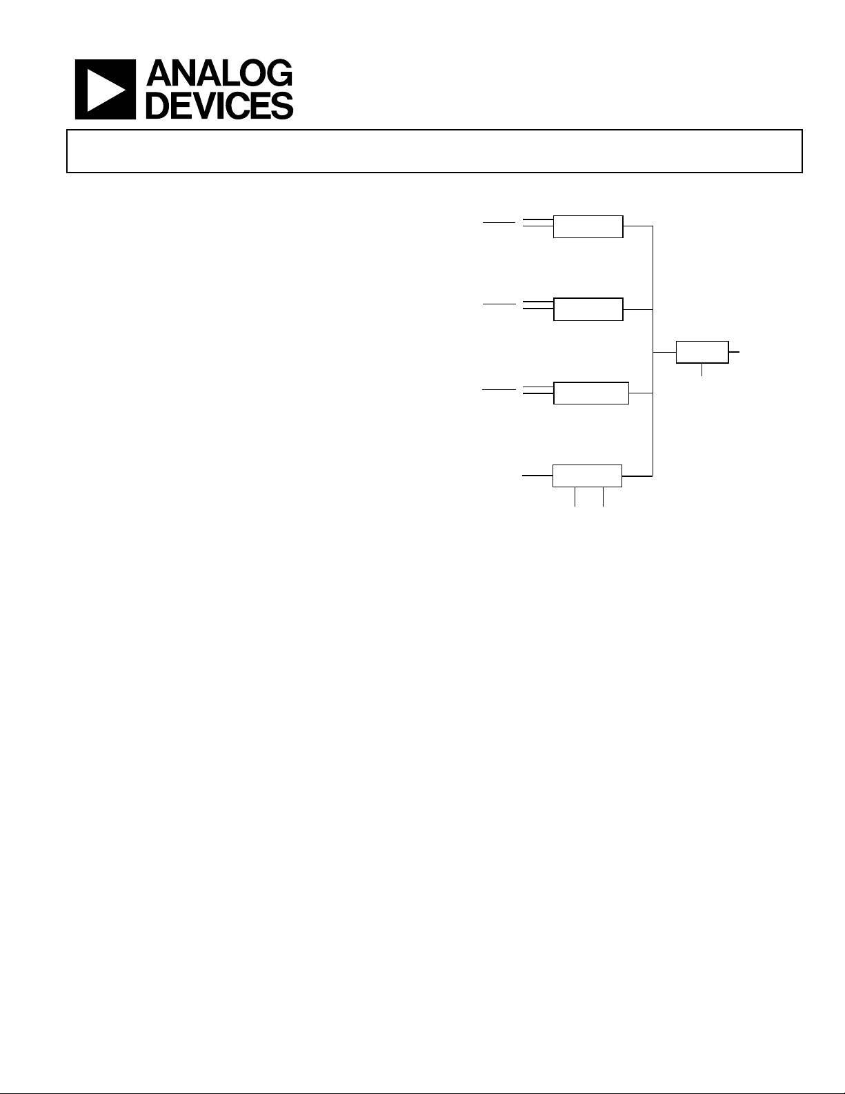
GENERAL DESCRIPTION
The AD9662 is a laser diode driver for high performance CD
and DVD recordable drives. It includes three channels for three
different optical power levels: the read channel generates a
continuous output power level, whereas Channel 2 and
Channel 3 are used as write channels having 0.8 ns rise/fall
times. All channel currents are summed at the I
channel’s output current is established by multiplying the
channel’s gain by the channel’s input current. The input current
for each of the input channels—INR, IN2, and IN3—can be set
either by using an external resistor that converts an input
voltage to a current or by directly using a current source.
pin. Each
OUT
with Oscillator
FUNCTIONAL BLOCK DIAGRAM
IN3
OUTEN3
IN2
OUTEN2
INR
OUTENR
OSCEN
CHANNEL 3
CHANNEL 2
READ CHANNEL
OSCILLATOR
R
R
S
F
Figure 1. AD9662 3-Channel Laser Diode Driver
AD9662
OUTPUT
ENABLE
I
OUT
04389-0-001
An on-chip oscillator is provided to allow output current
modulation (to reduce laser mode hopping). Two external
resistors control the frequency and the amplitude swing of the
oscillator. The push-pull oscillator can swing up to 100 mA p-p
and has a frequency range of 200 MHz to 500 MHz.
Rev. C
Information furnished by Analog Devices is believed to be accurate and reliable. However, no
responsibility is assumed by Anal og Devices for its use, nor for any infringements of patents or ot her
rights of third parties that may result from its use. Specifications subject to change without notice. No
license is granted by implication or otherwise under any patent or patent rights of Analog Devices.
Trademarks and registered trademarks are the property of their respective owners.
One Technology Way, P.O. Box 9106, Norwood, MA 02062-9106, U.S.A.
Tel: 781.329.4700 www.analog.com
Fax: 781.461.3113 © 2005 Analog Devices, Inc. All rights reserved.
Page 2

AD9662
TABLE OF CONTENTS
Features .............................................................................................. 1
Pin Configuration and Function Descriptions..............................6
Applications....................................................................................... 1
General Description......................................................................... 1
Functional Block Diagram .............................................................. 1
Revision History ............................................................................... 2
Specifications..................................................................................... 3
Absolute Maximum Ratings............................................................ 5
ESD Caution.................................................................................. 5
REVISION HISTORY
11/05—Rev. SpB to Rev. C
Changes to Format ............................................................. Universal
7/04—Rev. Sp0 to Rev. SpB
Changes to Note 2 in Specifications............................................... 4
Changes to Absolute Maximum Ratings....................................... 5
Changes to Figure 17...................................................................... 12
12/03—Rev. SpA: Initial 2-Page Web Version
Typical Perf or m an c e Character i st ic s ..............................................7
Applications..................................................................................... 10
Temperature Considerations .................................................... 10
Evaluation Board ............................................................................ 12
Outline Dimensions ....................................................................... 13
Ordering Guide .......................................................................... 13
12/03—Rev. Sp0: Initial Full Version
Rev. C | Page 2 of 16
Page 3

AD9662
SPECIFICATIONS
At T
, VCC = 5 V, ENABLE = 1, OSCEN = 0,
AMB
Table 1.
Parameter Conditions Min Typ Max Unit
LASER AMPLIFIER
Output Current Read Channel
Output Current Channel 2
Output Current Channel 3
Total Output Current
Output Current Linearity
Output Current Linearity
Output Current Linearity
Best-Fit Current Gain
Best-Fit Current Gain
Best-Fit Current Gain
Best-Fit Current Offset
Best-Fit Current Offset
Best-Fit Current Offset
I
Series Resistance Total R
OUT
1
1
1
1
1
1
1
1
1
Input Impedance (RIN), Channel R, Channel 2 RIN to GND 160 200 240 Ω
Input Impedance (RIN), Channel 3 RIN to GND 80 100 120 Ω
I
Supply Sensitivity (PSRR) I
OUT
Read Mode
I
Supply Sensitivity (PSRR) I
OUT
Write Mode
Output Current Noise
I
Temperature Sensitivity I
OUT
Read Mode
I
Temperature Sensitivity I
OUT
Write Mode Channel 2
I
Temperature Sensitivity I
OUT
Write Mode Channel 3
LASER AMPLIFIER AC SPECIFICATIONS
Write Rise Time
2
Write Fall Time
2
Output Current Overshoot I
I
ON Propagation Delay
OUT
I
OFF Propagation Delay
OUT
Disable Time ENABLE 50% H-L to I
Enable Time ENABLE 50% L-H to I
OSCILLATOR SPECIFICATIONS
Oscillator Frequency RF = 9.53 kΩ, RS = 23.7 kΩ 265 300 325 MHz
Oscillator Frequency Temperature Coefficient RF = 9.53 kΩ, RS = 23.7 kΩ 600 ppm/°C
Disable Time Oscillator OSCEN 50% H-L to amplitude at 50% of initial value 4 ns
Enable Time Oscillator OSCEN 50% L-H to amplitude at 50% of final value 6 ns
OUTENx
= 1, unless otherwise stated.
Output is sourcing,
Output is sourcing,
Output is sourcing,
Output is sourcing,
OUTENR
(
= 0 and/or
Read Channel,
Write2 Channel,
Write3 Channel,
Read Channel,
Write2 Channel,
Write3 Channel,
Read Channel,
Write2 Channel,
Write3 Channel,
to VCC rail 6.5 10 Ω
OUT
= 50 mA (read-only), VCC = 5 V ± 10% 10 15 %/V
OUT
OUTENR
OUT
= 0
= 100 mA (50 mA read, 50 mA write) 10 15 %/V
VCC = 5 V ± 10%,
OUTEN2
(
I
OUT
OUT
OUTENR
OUT
OUTENR
OUT
OUTENR
I
OUT
OUTENR
I
OUT
OUTENR
OUT
OUTENR
OUTENx
OUTENx
OUTENR
= 0 or
= 50 mA (Read),
= 50 mA (read-only) 100 ppm/°C
= 0
= 100 mA (50 mA Read, 50 mA Write2) 100 ppm/°C
= 0,
= 100 mA (50 mA Read, 50 mA Write3) 100 ppm/°C
= 0,
= 50 mA dc (Read), 50 mA pulse W2 or W3 0.8 1.8 ns
= 0 and (
= 50 mA dc (Read), 50 mA pulse W2 or W3 0.6 1.8 ns
= 0
= 50 mA dc (Read), 50 mA pulse W2 or W3 13 %
= 0 and (
50% H-L to I
50% L-H to I
= 0
OUTENR
OUTEN2
OUTEN3
OUTEN3
OUTENR
OUTEN2
OUTEN3
OUTENR
OUTEN2
OUTEN3
OUTENR
OUTEN2
OUTEN3
OUTENR
OUTEN3
OUTENR
OUTEN2
OUTEN3
OUTEN2
OUTEN2
OUT
OUT
OUT
OUT
= 0
= 0
= 0
= 0 and
OUTEN2
= 0)
= 0
= 0
= 0
= 0
= 0
= 0
= 0
= 0
= 0
= 0 and
= 0)
= 0, f = 300 MHz
= 0
= 0
OUTEN3
= 0 or
= 0 or
OUTEN3
= 0)
= 0)
at 50% of final value
at 50% of initial value
at 50% of initial value 5.4 ns
at 50% of final value 13.5 ns
210 235 mA
210 235 mA
315 340 mA
>550 mA
−4 ±0.6 +4 %
−4 ±0.6 +4 %
−4 ±0.1 +4 %
125 135 145 mA/mA
120 130 140 mA/mA
240 260 280 mA/mA
−7 ±0.6 +7 mA
−7 ±0.6 +7 mA
−30 −2 +15 mA
150 pA/√Hz
2.7 ns
2.7 ns
Rev. C | Page 3 of 16
Page 4

AD9662
Parameter Conditions Min Typ Max Unit
LOGIC SPECIFICATIONS
Logic HI Threshold 2.0 V
Logic LO Threshold 0.8 V
Input Impedance
Input Leakage Current
SUPPLY CURRENT ENABLE OSCEN
OUTENx
OUTENx
, ENABLE, OSCEN
, ENABLE, OSCEN
OUTENR OUTEN2 OUTEN3
Power-Down 0 0 1 1 1 8.5 10 mA
Power-Up
Inputs Disabled 1 0 1 1 1 18 22 mA
Inputs Disabled, OSC Enabled 1 1 1 1 1 52 62 mA
Read Mode, OSC Enabled
I
= 50 mA
OUT
Write Mode
I
OUT
3
= 100 mA (50 mA W2, 50 mA W3)
3
1 1 0 1 1 55 65 mA
1 0 1 0 0 29 35 mA
OPERATING CONDITIONS
Supply Voltage Range 4.5 5.5 V
Operating Temperature Range 0 85 °C
1
Output linearity, offset current, and gain are calculated using a best-fit method at 30 mA, 45 mA, 60 mA, 75 mA, and 90 mA for the Read and Write2 Channels and
90 mA, 105 mA, 120 mA, 135 mA, and 150 mA for Write Channel 3. Each channel’s output current is given by I
2
This parameter is guaranteed by design and characterization using six sigma. Rise and fall times are measured electrically from the 10% to 90% points using a Sharp
GH0781JA2C diode as a load.
3
The values specified do not include the output current.
= (IIN × Gain) + IOS.
OUT
>10 MΩ
<1 μA
Rev. C | Page 4 of 16
Page 5

AD9662
ABSOLUTE MAXIMUM RATINGS
Table 2.
Parameter Range
Supply Voltage +V
Pin 9, Pin 15, and Pin 16 5.5 V
Input Pins
Pin 1 and Pin 2 2.2 mA
Pin 5 1.6 mA
Pin 6, Pin 7, Pin 8, Pin 10, and Pin 11 −0.8 V to +5.5 V
Internal Power Dissipation
16-Lead QSOP 620 mW
Operating Temperature Range 0°C to +85°C
Storage Temperature Range −65°C to +150°C
Lead Temperature, Soldering 60 sec 300°C
1
Power dissipation is specified on SEMI standard 4-layer board.
S
1
Stresses above those listed under Absolute Maximum Ratings
may cause permanent damage to the device. This is a stress
rating only; functional operation of the device at these or any
other conditions above those indicated in the operational
section of this specification is not implied. Exposure to absolute
maximum rating conditions for extended periods may affect
device reliability.
ESD CAUTION
ESD (electrostatic discharge) sensitive device. Electrostatic charges as high as 4000 V readily accumulate on the
human body and test equipment and can discharge without detection. Although this product features
proprietary ESD protection circuitry, permanent damage may occur on devices subjected to high energy
electrostatic discharges. Therefore, proper ESD precautions are recommended to avoid performance
degradation or loss of functionality.
Rev. C | Page 5 of 16
Page 6

AD9662
PIN CONFIGURATION AND FUNCTION DESCRIPTIONS
INR
1
IN2
2
GND
3
R
4
F
AD9662
IN3
5
OUTENR
OUTEN2
OUTEN3
6
7
8
Figure 2. Pin Configuration
Table 3. Pin Function Descriptions
Pin No. Mnemonic Description
1 INR Input Current Pin for the Read Channel. Has a typical input impedance of 200 Ω.
2 IN2 Input Current Pin for Write Channel 2. Has a typical input impedance of 200 Ω.
3, 13 GND Common External Ground Reference.
4 R
F
Pin Used to Set Oscillator Frequency by Connecting a Resistor from This Pin to Ground.
5 IN3 Input Current Pin for Write Channel 3. Has a typical input impedance of 100 Ω.
6
7
8
9, 15, 16 V
OUTENR
OUTEN2
OUTEN3
CC
TTL-Compatible Enable for the Read Channel. Logic low active.
TTL-Compatible Enable for Write Channel 2. Logic low active.
TTL-Compatible Enable for Write Channel 3. Logic low active.
Power Supply Pins for the AD9662. Each pin needs to be decoupled with a 0.1 μF capacitor to ground.
10 OSCEN TTL-Compatible Enable for the Oscillator. Logic high active.
11 ENABLE TTL-Compatible Enable for the Device. Logic high active.
12 R
14 I
S
OUT
Pin Used to Set Oscillator Amplitude by Connecting a Resistor from This Pin to Ground.
Output Current Pin. This pin is connected to the anode of a laser diode.
16
15
14
13
12
11
10
9
V
CC
V
CC
I
OUT
GND
R
S
ENABLE
OSCEN
V
CC
04389-0-002
Rev. C | Page 6 of 16
Page 7

AD9662
TYPICAL PERFORMANCE CHARACTERISTICS
RS = 23.7 kΩ, RF = 9.53 kΩ, and read channel output current is 50 mA, unless otherwise noted.
500
400
300
200
100
OSCILLATOR FREQUENCY (MHz)
0
0
RF RESISTANCE (kΩ)
Figure 3. Oscillator Frequency vs. R
105
15 20
F
04389-0-003
150
140
130
120
110
100
90
80
70
60
50
40
30
20
OSCILLATOR AMPLITUDE (mA p-p)
10
0
0
RS RESISTANCE (kΩ)
100 12060 8020 40
Figure 6. Oscillator Amplitude vs. R
S
140 160
04389-0-006
70
60
50
40
30
20
10
OSCILLATOR AMPLITUDE (mA p-p)
0
200
1.40
1.20
1.00
0.80
0.60
0.40
CURRENT NOISE (nA/ Hz)
0.20
0.00
0.1
300
FREQUENCY (MHz)
400 500
Figure 4. Oscillator Amplitude vs. Frequency
FREQUENCY (MHz)
Figure 5. I
10
Current Noise
OUT
1001
1000
04389-0-004
04389-0-005
130
120
110
100
90
80
SUPPLY CURRENT (mA)
70
60
0
10 14020 30 40 50 60 70 80 90
OSCILLATOR AMPLITUDE (mA p-p)
110
120100
Figure 7. Supply Current vs. Oscillator Amplitude
–20
–30
–40
–50
–60
DISTORTION (dBc)
–70
FIFTH HARMONIC
–80
200 250 300 350 400 450 500
OSCILLATOR FREQUENCY (MHz)
THIRD HARMONIC
SECOND HARMONIC
FOURTH HARMONIC
Figure 8. Oscillator Harmonic Distortion vs. Frequency
130 150
04389-0-007
04389-0-008
Rev. C | Page 7 of 16
Page 8

AD9662
55
50
305
300
295
45
40
OSCILLATOR AMPLITUDE (mA p-p)
35
–40
–20 40 800
20 60 100
TEMPERATURE (°C)
Figure 9. Oscillator Amplitude vs. Temperature
μW
10ns/DIV
Figure 10. Optical Response 50 mA Read, 50 mA Write2,
Sharp GH0781JA2C Diode
225
200
175
150
125
(mA)
100
OUT
I
75
50
25
0
0.50 1.0 1.5 2.0 2.5 3.0 3.5 4.0 4.5 5.0
(VCC– V (I
OUT
)) (Volts)
Figure 11. Output Current vs. Voltage Compliance
04389-0-009
04389-0-010
04389-0-011
290
285
OSCILLATOR FREQUENCY (MHz)
280
275
μW
WRITE PULSE
ZERO LEVEL
OUTEN3
OUTEN2
OUTENR
–40
–20 40 800
20 60 100
TEMPERATURE (°C)
Figure 12. Oscillator Frequency vs. Temperature
10ns/DIV
Figure 13. Optical Response 50 mA Read, 200 mA Write3,
Sharp GH0781JA2C Diode
P
w
BIAS LEVEL
OUTPUT WAVEFORM
P
b
T
ERASE LEVEL
Figure 14. Typical Waveform
04389-0-012
04389-0-013
P
e
04389-0-017
Rev. C | Page 8 of 16
Page 9

AD9662
Table 4. I
ENABLE
0 X X X Off
1 1 1 1 Off
1 0 1 1 (I
1 1 0 1 (I
1 1 1 0 (I
Table 5. Oscillator Control
ENABLE OSCEN
0 X X X X Off
1 0 X X X Off
1 1 1 1 1 On
1 1 0 X X On
1 1 X 0 X On
1 1 X X 0 On
Control
OUT
OUTENR OUTEN2 OUTEN3
OUTENR OUTEN2 OUTEN3
I
OUT
× GainR) + I
INR
× Gain2) + I
IN2
× Gain3) + I
IN3
OSR
OS2
OS3
OSCILLATOR
Rev. C | Page 9 of 16
Page 10

AD9662
APPLICATIONS
The AD9662 uses the current at one or more of its three
, I
inputs—I
INR
IN2
, and I
proportional to the input currents. Channel R has a typical gain
of 135 mA/mA, Channel 2 has a typical gain of 130 mA/mA,
and Channel 3 has a typical gain of 260 mA/mA. The input
impedance of Channel R and Channel 2 is typically 200 Ω, and
the input impedance of Channel 3 is typically 100 Ω. In most
cases, a voltage output DAC is used to set the dc current of
these channels. A series resistor should be placed between each
DAC’s output and its respective input channel. These resistors
should be chosen to properly scale the input current while not
excessively loading the output of the DAC.
Channel R is used to provide bias current to the laser diode, and
Channel 2 and Channel 3 are used to set the amplitudes of the
current pulses that are required to write or erase the media. The
output pulses are created by applying TTL level pulses to the
channel enable pins while dc current is flowing into the input
pins. Channel 2 and Channel 3 are turned on and off according
to a predetermined write strategy (see
Due to the fast rise and fall time (<1 ns) required for the
operation of higher speed drives, trace lengths carrying high
speed signals, such as ENR, EN2, EN3, and the output current,
should be kept as short as possible to minimize series inductance.
A decoupling capacitor should be located near each V
and the ground return for the cathode of the laser diode should
be kept as short as possible.
Rise time, t
, is defined as the time a pulse requires to transition
r
from 10% of its final value to 90% of its final value. Appropriately,
fall time, t
, is defined as the time a pulse requires to go from
f
90% of its initial value to 10% of its initial value.
Propagation delay is defined as the time when a transitioning
logic signal reaches 50% of its amplitude to when the output
current, I
, reaches 50% of its amplitude.
OUT
TEMPERATURE CONSIDERATIONS
The AD9662 is in a 16-lead QSOP. JEDEC methods were used
to determine the θ
efficient thermally conductive test board (or 4-layer board).
This board is made of FR4, is 1.60 mm thick, and consists of
four copper layers. The two internal layers are solid copper
(1 ounce/in
(containing the component and back side traces) use
2 ounces/in
construction yields a θ
105°C/W. An integrated circuit dissipating 500 mW and
packaged in a QSOP, while operating in an ambient
environment of 85°C, has an internal junction temperature
of approximately 138°C.
2
or 0.35 mm thick). The two surface layers
2
(0.70 mm thick) copper. This method of
85°C + 0.500 W × 105°C/W = 138°C
—and generates an output current
IN3
Figure 14).
pin,
CC
of the QSOP when mounted on a highly
JA
for the AD9662 of approximately
JA
This junction temperature is within the maximum recommended
operating junction temperature of 150°C. Of course, this is not
a realistic method for mounting a laser diode driver in an
optical storage device. In an actual application, the laser diode
driver would most likely be mounted to a flexible circuit board.
The θ
of a system is highly dependent on board layout and
JA
material. The user must consider these conditions carefully.
Some of the circuitry of the AD9662 can be used to monitor the
internal junction temperature. The AD9662 uses diodes to
protect it from electrostatic discharge (ESD). Every input pin
has a diode between it and ground, with the anode connected to
ground and the cathode connected to the particular input pin.
The base-emitter junction of a PNP transistor is used for ESD
protection from each pin to V
connected to the substrate of the die (see
. The collector is electrically
CC
Figure 15). The baseemitter junction of this transistor can be used to monitor the
internal die temperature of the IC.
Using a 10 V source at the enable pin to forward-bias the
base-emitter junction and a 1 MΩ resistor to limit the current, a
2-point measurement can be used to calculate the junction
temperature of the IC. Because the enable pin (ENABLE) needs
to be a logic high for normal operation, the AD9662 can be
operated with the 10 V applied through the 1 MΩ resistor.
The first point is obtained by measuring the voltage, V1, with
= 0 immediately after the AD9662 is turned on. The case
I
OUT
temperature, T1, can be measured using a thermocouple. The
temperature of the case is measured immediately after the IC is
turned on, and that temperature is the temperature of the
transistor junction and of the die itself. Through characterization
of the AD9662, it was determined that the forward-bias voltage
of the base-emitter junction of the transistor decreases by
1.9 mV for every 1°C rise in junction temperature.
The second point of the 2-point measurement is obtained when
the AD9662 is operated under load. I
is adjusted until the
OUT
increase in supply current is 200 mA. The AD9662 is allowed to
reach thermal equilibrium, and then the voltage, V2, is measured.
The voltage measurements taken with the IC running are lower
than the actual base-emitter drop across the transistor due to
the voltage drops across the internal resistance that is in series
with the supply current (see
Figure 15). This finite resistance
was calculated to be approximately 120 mΩ. Therefore, for a
supply current change of 200 mA, the ΔV
calculation is
BE
24 mV too low. Therefore, 24 mV must be added to the
difference in measured voltages. The change in the baseemitter voltage is then calculated.
= (V2 + 24 mV – V1)
ΔV
BE
Rev. C | Page 10 of 16
Page 11

AD9662
The change in junction temperature can then be determined.
T
= T1 + ΔVBE/(1.9 mV/°C)
J
AD9662
I
CC
V
CC
R
S
5V
10V
1MΩ
–
V1, V2
+
ENR
GND
I
BE
04389-0-015
Figure 15. Junction Temperature Measurement Circuit
This 2-point measurement allows the rise in die temperature to
be calculated for any given power dissipation. The θ
of the
JA
system can be calculated using the power dissipation of the LDD.
= VCC × ICC – V
P
D
θJA = (TJ – T1)/P
D
DIODE
× I
DIODE
Using the preceding method, actual data was taken to
determine the θ
Immediately after
of the AD9662 in the evaluation board.
JA
power-up, V1 was measured to be 593 mV.
The supply current was 27 mA. The AD9662 was adjusted to
deliver 200 mA into a 10 Ω load. This resulted in a total supply
current of 244 mA. After allowing the part to reach thermal
equilibrium, V2 measured 412 mV. The voltage drop across the
120 mΩ internal resistor due to the change in supply current
was then calculated.
(244 mA – 27 mA) × 120 mΩ = 26 mV
This 26 mV internal voltage drop was then added to the
measured voltage reduction to determine the actual ΔV
BE.
ΔVBE = (593 mV – 412 mV + 26 mV) = 207 mV
The die temperature change measured 82.4°C. The output of
the AD9662 was at a voltage of 2 V. The part dissipated an
additional 600 mW of power (3 V × 200 mA). The θ
for the
JA
AD9962 mounted on its 2-layer board was calculated to be:
600 mW/82.4°C = 137°C/W.
0.7
0.6
Figure 16 shows a graph of the measured voltage between ENR
(V
and V
− VCC) vs. the die temperature. This graph was
CC
ENR
constructed using a 2-layer evaluation board for the AD9662
Figure 17).
(see
(V)
– V
V
0.5
0.4
CC
0.3
ENR
0.2
0.1
0
4020 60 80 100 120 140 160
Figure 16. V
TEMPERATURE (°C)
− VCC vs. Internal Temperature
ENR
04389-0-014
Rev. C | Page 11 of 16
Page 12

AD9662
EVALUATION BOARD
VINR
ENR
EN2
EN3
50Ω
50Ω
50Ω
C3
0.1μF
C2
0.1μF
C4
0.1μF
R8
R7
R6
VINR
VINW2
VIN2
VINW3
VIN3
W1
DNI
W2
DNI
W3
DNI
R2
4.32kΩ
R3
4.32kΩ
R5
4.32kΩ
5V
5V
5V
R4
9.53kΩ
V
S
DUT1
INR
1
IN2
2
GND
3
R
4
IN3
5
OUTENR
6
7
OUTEN2
8
OUTEN3
F
V
V
I
OUT
GND
ENABLE
OSCEN
V
16
CC
15
CC
14
13
12
R
S
11
10
9
CC
AD9662
V
5V
D
R13
5kΩ
C9
0.1μF
GND
V
S
C7
10μF
C1
0.1μF
R9
23.7kΩ
C5
0.1μF
R1
3.1Ω
DNI
D1
R10
DNI
R11
50Ω
R12
46.4Ω
V_OUT
CHIP_EN
OSCEN
R17
DNI
C8
DNI
5V
W5
5V
W4
DNI
Figure 17. AD9662 QSOP-16 Evaluation Board Schematic
Note: If dc logic levels are desired on the enable pins, then Jumper W1 through Jumper W5 should be used, and Resistor R6 through
Resistor R11 should not be installed. If the enable pins are driven from external signal sources, then these resistors should be
installed, and the jumpers are not necessary.
04389-0-016
Rev. C | Page 12 of 16
Page 13

AD9662
OUTLINE DIMENSIONS
0.197
0.193
0.189
0.012
0.008
9
8
0.158
0.154
0.150
0.069
0.053
SEATING
PLANE
0.244
0.236
0.228
0.010
0.006
8°
0°
0.050
0.016
0.065
0.049
0.010
0.004
COPLANARITY
0.004
16
1
PIN 1
0.025
BSC
COMPLIANT TO JEDEC STANDARDS MO-137-AB
Figure 18.16-Lead Shrink Small Outline Package [QSOP]
(RQ-16)
Dimensions shown in inches
ORDERING GUIDE
Model Temperature Range Package Description Package Option
AD9662ARQZ
AD9662ARQZ-REEL
AD9662ARQZ-REEL7
1
Z = Pb-free part.
1
1
1
0°C to 85°C 16-Lead QSOP RQ-16
0°C to 85°C 16-Lead QSOP RQ-16
0°C to 85°C 16-Lead QSOP RQ-16
Rev. C | Page 13 of 16
Page 14

AD9662
NOTES
Rev. C | Page 14 of 16
Page 15

AD9662
NOTES
Rev. C | Page 15 of 16
Page 16

AD9662
NOTES
© 2005 Analog Devices, Inc. All rights reserved. Trademarks and
registered trademarks are the property of their respective owners.
C04389-0-11/05(C)
Rev. C | Page 16 of 16
 Loading...