

Page 1
14-Bit, 80 MSPS/155 MSPS, 1.8 V Dual
A
A
Serial Output Analog-to-Digital Converter (ADC)
FEATURES
JESD204A coded serial digital outputs
SNR = 73.7 dBFS at 70 MHz and 80 MSPS
SNR = 71.7 dBFS at 70 MHz and 155 MSPS
SFDR = 92 dBc at 70 MHz and 80 MSPS
SFDR = 92 dBc at 70 MHz and 155 MSPS
Low power: 423 mW at 80 MSPS, 567 mW at 155 MSPS
1.8 V supply operation
Integer 1-to-8 input clock divider
IF sampling frequencies to 250 MHz
−148.6 dBFS/Hz input noise at 180 MHz and 80 MSPS
−150.3 dBFS/Hz input noise at 180 MHz and 155 MSPS
Programmable internal ADC voltage reference
Flexible analog input range: 1.4 V p-p to 2.1 V p-p
ADC clock duty cycle stabilizer
Serial port control
User-configurable, built-in self-test (BIST) capability
Energy-saving power-down modes
APPLICATIONS
Communications
Diversity radio systems
Multimode digital receivers (3G and 4G)
GSM, EDGE, W-CDMA, LTE,
CDMA2000, WiMAX, TD-SCDMA
I/Q demodulation systems
Smart antenna systems
General-purpose software radios
Broadband data applications
Ultrasound equipment
AD9644
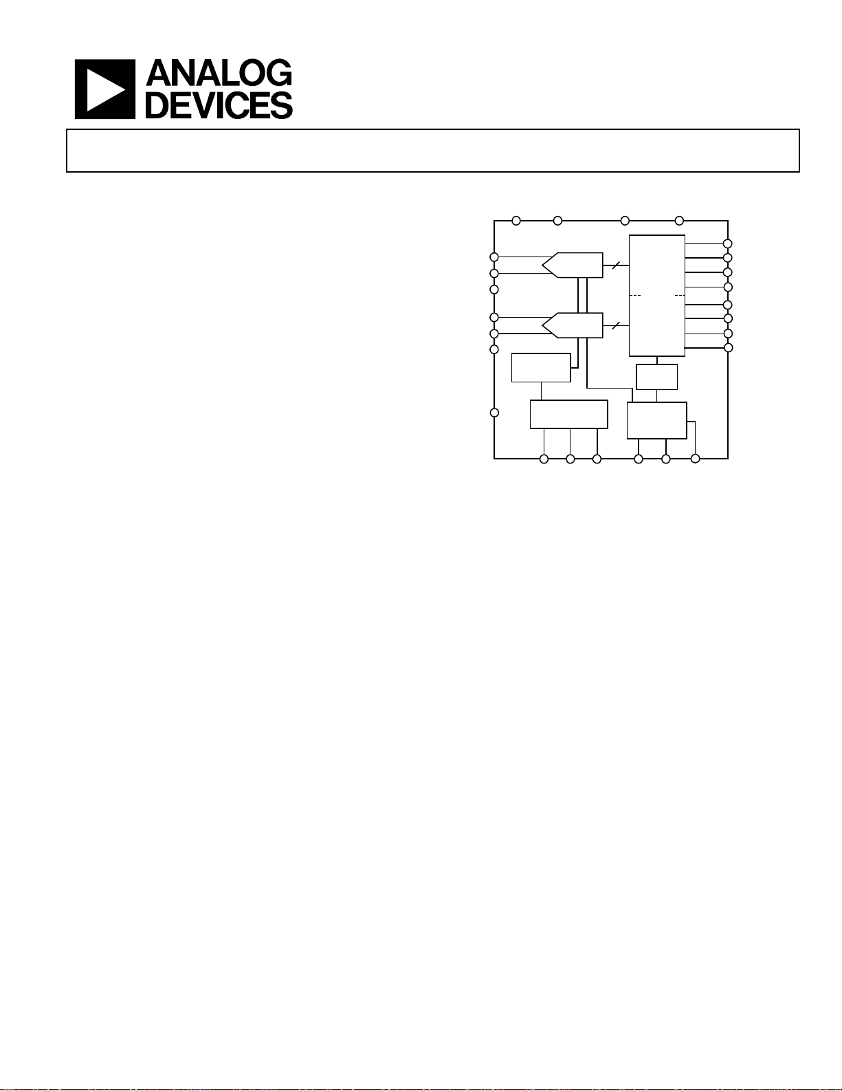
FUNCTIONAL BLOCK DIAGRAM
VDD
GND
AD9644
VIN+A
VIN–A
VCMA
VIN+B
VIN–B
VCMB
PDWN
PIPELINE
14-BIT ADC
PIPELINE
14-BIT ADC
REFERENCE
SERIAL PORT
(SPI)
SCLK SDIO CSB
Figure 1. 48-Lead 7 mm × 7 mm LFCSP
PRODUCT HIGHLIGHTS
1. An on-chip PLL allows users to provide a single ADC
sampling clock; the PLL multiplies the ADC sampling
clock to produce the corresponding JESD204A data rate
clock.
2. The configurable JESD204A output block supports up to
1.6 Gbps per channel data rate when using a dedicated
data link per ADC or 3.2 Gbps data rate when using a
single shared data link for both ADCs.
3. Proprietary differential input that maintains excellent SNR
performance for input frequencies up to 250 MHz.
4. Operation from a single 1.8 V power supply.
5. Standard serial port interface (SPI) that supports various
product features and functions, such as data formatting
(offset binary, twos complement, or gray coding),
controlling the clock DCS, power-down, test modes,
voltage reference mode, and serial output configuration.
DRVDD DRGND
14
14
JESD204A 8-BIT/ 10-BIT
CODING, SE RIALIZER AND
PLL
1 TO 8
CLOCK
DIVIDER
CLK+ CLK–
CML DRIVERS
DOUT+A
DOUT–A
DSYNC+A
DSYNC–A
DOUT+B
DOUT–B
DSYNC+B
DSYNC–B
SYNC
9180-001
Rev. B
Information furnished by Analog Devices is believed to be accurate and reliable. However, no
responsibility is assumed by Anal og Devices for its use, nor for any infringements of patents or ot her
rights of third parties that may result from its use. Specifications subject to change without notice. No
license is granted by implication or otherwise under any patent or patent rights of Analog Devices.
Trademarks and registered trademarks are the property of their respective owners.
One Technology Way, P.O. Box 9106, Norwood, MA 02062-9106, U.S.A.
Tel: 781.329.4700 www.analog.com
Fax: 781.461.3113 ©2010–2011 Analog Devices, Inc. All rights reserved.
Page 2

AD9644
TABLE OF CONTENTS
Features.............................................................................................. 1
Applications....................................................................................... 1
Functional Block Diagram .............................................................. 1
Product Highlights ........................................................................... 1
Revision History ............................................................................... 2
General Description ......................................................................... 3
Specifications..................................................................................... 4
ADC DC Specifications................................................................. 4
ADC AC Specifications ................................................................. 5
Digital Specifications ................................................................... 6
Switching Specifications................................................................ 8
Timing Specifications .................................................................. 9
Absolute Maximum Ratings.......................................................... 10
Thermal Characteristics ................................................................ 10
ESD Caution................................................................................ 10
Pin Configuration and Function Descriptions........................... 11
Typical Performance Characteristics ........................................... 13
Equivalent Circuits......................................................................... 19
Theory of Operation ...................................................................... 20
ADC Architecture ......................................................................20
Analog Input Considerations.................................................... 20
Voltage Reference ....................................................................... 22
Clock Input Considerations...................................................... 22
Channel/Chip Synchronization................................................ 24
Power Dissipation and Standby Mode .................................... 24
Digital Outputs........................................................................... 24
Built-In Self-Test (BIST) and Output Test .................................. 29
Built-In Self-Test (BIST)............................................................ 29
Output Test Modes..................................................................... 29
Serial Port Interface (SPI).............................................................. 31
Configuration Using the SPI..................................................... 31
Hardware Interface..................................................................... 32
SPI Accessible Features.............................................................. 32
Memory Map .................................................................................. 33
Reading the Memory Map Register Table............................... 33
Memory Map Register Table..................................................... 34
Memory Map Register Descriptions........................................ 38
Applications Information.............................................................. 42
Design Guidelines ...................................................................... 42
Outline Dimensions....................................................................... 43
Ordering Guide .......................................................................... 43
REVISION HISTORY
6/11—Rev. A to Rev. B
Added Figure 23 to Figure 40; Renumbered Sequentially ........ 16
Changes to Clock Input Considerations Section........................ 22
Added Figure 61.............................................................................. 24
Changes to Digital Outputs and Timing Section ....................... 27
Added Figure 69.............................................................................. 28
Changes to Output Test Modes Section ...................................... 29
Changes to SPI Accessible Features Section ............................... 32
4/11—Rev. 0 to Rev. A
Added Model -155......................................................... Throughout
Changes to Features Section and Figure 1 .....................................1
Changes to General Description Section .......................................3
Changes to Table 1.............................................................................4
Changes to Table 2.............................................................................5
Changes to Table 4.............................................................................8
Additions to TPC Introductory Statement ................................. 13
Changes to Speed Grade ID Bits in Table 17 .............................. 31
Changes to Ordering Guide.......................................................... 40
6/10—Revision 0: Initial Version
Rev. B | Page 2 of 44
Page 3

AD9644
GENERAL DESCRIPTION
The AD9644 is a dual, 14-bit, analog-to-digital converter (ADC)
with a high speed serial output interface and sampling speeds
of either 80 MSPS or 155 MSPS.
The AD9644 is designed to support communications applications where high performance, combined with low cost, small
size, and versatility, is desired. The JESD204A high speed serial
interface reduces board routing requirements and lowers pin count
requirements for the receiving device.
The dual ADC core features a multistage, differential pipelined
architecture with integrated output error correction logic. Each
ADC features wide bandwidth differential sample-and-hold
analog input amplifiers that support a variety of user-selectable
input ranges. An integrated voltage reference eases design considerations. A duty cycle stabilizer is provided to compensate for
variations in the ADC clock duty cycle, allowing the converters
to maintain excellent performance.
By default the ADC output data is routed directly to the two
external JESD204A serial output ports. These outputs are at CML
voltage levels. Two modes are supported such that output coded
data is either sent through one data link or two. (L = 1; F = 4 or
L = 2; F = 2). Independent synchronization inputs (DSYNC) are
provided for each channel.
Flexible power-down options allow significant power savings,
when desired.
Programming for setup and control is accomplished using a 3-wire
SPI-compatible serial interface.
The AD9644 is available in a 48-lead LFCSP and is specified over
the industrial temperature range of −40°C to +85°C.
Rev. B | Page 3 of 44
Page 4

AD9644
SPECIFICATIONS
ADC DC SPECIFICATIONS
AVDD = 1.8 V, DRVDD = 1.8 V, maximum sample rate, 1.75 V p-p differential input, VIN = −1.0 dBFS differential input, DCS enabled,
unless otherwise noted.
Table 1.
AD9644-80 AD9644-155
Parameter Temperature Min Typ Max Min Typ Max Unit
RESOLUTION Full 14 14 Bits
ACCURACY
No Missing Codes Full Guaranteed Guaranteed
Offset Error Full ±2 ±10 ±2.2 ±11 mV
Gain Error Full −7 −2.5 +1 −6 −1.5 +4 % FSR
Differential Nonlinearity (DNL)1 Full ±0.55 ±0.55 LSB
25°C ±0.3 ±0.3 LSB
Integral Nonlinearity (INL)1 Full ±1.1 ±1.25 LSB
25°C ±0.5 ±0.55 LSB
MATCHING CHARACTERISTIC
Offset Error Full −7 +1.5 +10 −6 +1.5 +9 mV
Gain Error Full −1.5 +0.6 +2.75 −3.1 +0.75 +5 % FSR
TEMPERATURE DRIFT
Offset Error Full ±2 ±2 ppm/°C
Gain Error Full ±35 ±144 ppm/°C
INPUT REFERRED NOISE 25°C 0.7 0.7 LSB rms
ANALOG INPUT
Input Span Full 1.383 1.75 2.087 1.383 1.75 2.087 V p-p
Input Capacitance2 Full 7 5 pF
Input Resistance Full 20 20 kΩ
VCM OUTPUT LEVEL Full 0.88 0.9 0.92 0.87 0.9 0.93 V
POWER SUPPLIES
Supply Voltage
AVDD Full 1.7 1.8 1.9 1.7 1.8 1.9 V
DRVDD Full 1.7 1.8 1.9 1.7 1.8 1.9 V
Supply Current
IAVDD1 Full 175 190 226 242 mA
IDRVDD1 Full 60 67 89 97 mA
POWER CONSUMPTION
Sine Wave Input1 Full 423 460 567 610 mW
Standby Power3 Full 85 168 mW
Power-Down Power Full 15 27 18 27 mW
1
Measured with a low input frequency, full-scale sine wave.
2
Input capacitance refers to the effective capacitance between one differential input pin and AGND.
3
Standby power is measured with a dc input and with the CLK pins inactive (set to AVDD or AGND).
Rev. B | Page 4 of 44
Page 5

AD9644
ADC AC SPECIFICATIONS
AVDD = 1.8 V, DRVDD = 1.8 V, maximum sample rate, 1.75 V p-p differential input, VIN = −1.0 dBFS differential input, DCS enabled,
unless otherwise noted.
Table 2.
AD9644-80 AD9644-155
Parameter1 Temperature Min Typ Max Min Typ Max Unit
SIGNAL-TO-NOISE-RATIO (SNR)
fIN = 10 MHz 25°C 73.8 71.9 dBFS
fIN = 70 MHz 25°C 73.7 71.7 dBFS
fIN = 180 MHz
AD9644BCPZ-80
AD9644CCPZ-80
AD9644BCPZ-155
fIN = 220 MHz 25°C 72.0 71.0 dBFS
SIGNAL-TO-NOISE AND DISTORTION (SINAD)
fIN = 10 MHz 25°C 72.7 70.8 dBFS
fIN = 70 MHz 25°C 72.6 70.7 dBFS
fIN = 180 MHz 25°C 71.5 70.3 dBFS
AD9644BCPZ-80
AD9644CCPZ-80
AD9644BCPZ-155
fIN = 220 MHz 25°C 71.1 69.9 dBFS
EFFECTIVE NUMBER OF BITS (ENOB)
fIN = 10 MHz
fIN = 70 MHz
fIN = 180 MHz
fIN = 220 MHz
WORST SECOND OR THIRD HARMONIC
fIN = 10 MHz
fIN = 70 MHz
fIN = 180 MHz
AD9644BCPZ-80
AD9644CCPZ-80
AD9644BCPZ-155
fIN = 220 MHz
SPURIOUS-FREE DYNAMIC RANGE (SFDR)
fIN = 10 MHz
fIN = 70 MHz
fIN = 180 MHz
AD9644BCPZ-80
AD9644CCPZ-80
AD9644BCPZ-155
fIN = 220 MHz
WORST OTHER (HARMONIC OR SPUR)
fIN = 10 MHz
fIN = 70 MHz
fIN = 180 MHz
AD9644BCPZ-80
AD9644CCPZ-80
AD9644BCPZ-155
fIN = 220 MHz
25°C 72.6 71.4 dBFS
Full 71.8 dBFS
Full 70.0 dBFS
Full 69.8 dBFS
Full 70.4 dBFS
Full 68.6 dBFS
Full 68.7 dBFS
25°C
25°C
25°C
25°C
25°C
25°C
25°C
Full
−94
−92
−87
−80
Full −73
Full
25°C
25°C
25°C
25°C
Full
−85
94
92
87
80
Full 73
Full
25°C
25°C
25°C
25°C
Full
Full
Full
25°C
85
−98
−98
−96
−90
−87
−95
11.8
11.8
11.6
11.5
11.5 Bits
11.5 Bits
11.4 Bits
11.3 Bits
−94 dBc
−92
−92 dBc
dBc
dBc
dBc
−90
−80
dBc
dBc
94 dBc
92 dBc
92 dBc
dBc
dBc
80 dBc
90 dBc
−97
−97
−95
dBc
dBc
dBc
dBc
dBc
−94
−89
dBc
dBc
Rev. B | Page 5 of 44
Page 6

AD9644
AD9644-80 AD9644-155
Parameter1 Temperature Min Typ Max Min Typ Max Unit
TWO-TONE SFDR
fIN = +30 MHz (−7 dBFS ), +33 MHz (−7 dBFS )
fIN = +169 MHz (−7 dBFS ), +172 MHz (−7 dBFS )
CROSSTALK2
ANALOG INPUT BANDWIDTH3
1
See the AN-835 Application Note, Understanding High Speed ADC Testing and Evaluation, for a complete set of definitions.
2
Crosstalk is measured at 100 MHz with −1.0 dBFS on one channel and no input on the alternate channel.
3
Analog input bandwidth specifies the −3 dB input BW of the AD9644 input. The usable full-scale BW of the part with good performance is 250 MHz.
25°C
25°C
Full
25°C
93
89
−105
780
DIGITAL SPECIFICATIONS
AVDD = 1.8 V, DRVDD = 1.8 V, maximum sample rate, 1.75 V p-p differential input, VIN = −1.0 dBFS differential input, and DCS enabled,
unless otherwise noted.
Table 3.
AD9644-80/AD9644-155
Parameter Temperature Min Typ Max Unit
DIFFERENTIAL CLOCK INPUTS (CLK+, CLK−)
Logic Compliance CMOS/LVDS/LVPECL
Internal Common-Mode Bias Full 0.9 V
Differential Input Voltage Full 0.3 3.6 V p-p
Input Voltage Range Full AGND AVDD V
Input Common-Mode Range Full 0.9 1.4 V
High Level Input Current Full −100 +100 μA
Low Level Input Current Full −100 +100 μA
Input Capacitance Full 4 pF
Input Resistance Full 8 10 12 kΩ
SYNC INPUT
Logic Compliance CMOS
Internal Bias Full 0.9 V
Input Voltage Range Full AGND AVDD V
High Level Input Voltage Full 1.2 AVDD V
Low Level Input Voltage Full AGND 0.6 V
High Level Input Current Full −100 +100 μA
Low Level Input Current Full −100 +100 μA
Input Capacitance Full 1 pF
Input Resistance Full 12 16 20 kΩ
DSYNC INPUT
Logic Compliance CMOS/LVDS
Internal Bias Full 0.9 V
Input Voltage Range Full AGND AVDD V
High Level Input Voltage Full 1.2 AVDD V
Low Level Input Voltage Full AGND 0.6 V
High Level Input Current Full −100 +100 μA
Low Level Input Current Full −100 +100 μA
Input Capacitance Full 1 pF
Input Resistance Full 12 16 20 kΩ
90 dBc
89 dBc
−105 dB
780 MHz
Rev. B | Page 6 of 44
Page 7

AD9644
AD9644-80/AD9644-155
Parameter Temperature Min Typ Max Unit
LOGIC INPUT (CSB)1
Logic Compliance CMOS
High Level Input Voltage Full 1.22 2.1 V
Low Level Input Voltage Full 0 0.6 V
High Level Input Current Full −10 +10 μA
Low Level Input Current Full 40 132 μA
Input Resistance Full 26 kΩ
Input Capacitance Full 2 pF
LOGIC INPUT (SCLK, PDWN)2
Logic Compliance CMOS
High Level Input Voltage Full 1.22 2.1 V
Low Level Input Voltage Full 0 0.6 V
High Level Input Current (VIN = 1.8 V) Full −92 −135 μA
Low Level Input Current Full −10 +10 μA
Input Resistance Full 26 kΩ
Input Capacitance Full 2 pF
LOGIC INPUT/OUTPUT (SDIO)1
Logic Compliance CMOS
High Level Input Voltage Full 1.22 2.1 V
Low Level Input Voltage Full 0 0.6 V
High Level Input Current Full −10 +10 μA
Low Level Input Current Full 38 128 μA
Input Resistance Full 26 kΩ
Input Capacitance Full 5 pF
DIGITAL OUTPUTS
Logic Compliance Full CML
Differential Output Voltage (VOD) Full 0.6 0.8 1.1 V
Output Offset Voltage (VOS) Full 0.75 DRVDD/2 1.05 V
1
Pull up.
2
Pull down.
Rev. B | Page 7 of 44
Page 8

AD9644
SWITCHING SPECIFICATIONS
AVDD = 1.8 V, DRVDD = 1.8 V, maximum sample rate, 1.75 V p-p differential input, VIN = −1.0 dBFS differential input, and DCS enabled,
unless otherwise noted.
Table 4.
AD9644-80 AD9644-155
Parameter Temperature Min Typ Max Min Typ Max Unit
CLOCK INPUT PARAMETERS
Input Clock Rate Full 640 640 MHz
Conversion Rate1 Full 40 80 40 155 MSPS
CLK Period—Divide-by-1 Mode (t
CLK Pulse Width High (tCH)
Divide-by-1 Mode, DCS Enabled Full 3.75 6.25 8.75 1.935 3.225 4.515 ns
Divide-by-1 Mode, DCS Disabled Full 5.95 6.25 6.55 3.065 3.225 3.385 ns
Divide-by-2 Mode Through Divide-by-8
Mode
Aperture Delay (tA) Full 0.78 0.78 ns
Aperture Uncertainty (Jitter, tJ) Full 0.125 0.125 ps rms
DATA OUTPUT PARAMETERS
Data Output Period or UI (Unit Interval) Full 1/(20 × f
Data Output Duty Cycle
Data Valid Time
PLL Lock Time (t
LOCK
)
Wake Up Time (Standby)
Wake Up Time (Power-Down)2 25°C 2.5 2.5 ms
Pipeline Delay (Latency) Full 23 24 23 24
Data Rate per Channel (NRZ)
Deterministic Jitter
Random Jitter at 1.6 Gbps
Random Jitter at 3.2 Gbps
Output Rise/Fall Time
TERMINATION CHARACTERISTICS
Differential Termination Resistance
OUT-OF-RANGE RECOVERY TIME
1
Conversion rate is the clock rate after the divider.
2
Wake-up time is defined as the time required to return to normal operation from power-down mode.
) Full 12.5 6.45 ns
CLK
Full 0.8 0.8 ns
25°C
25°C
25°C
25°C
) 1/(20 × f
CLK
50
50 %
0.78 0.74 UI
4 4 μs
5
5 μs
) Seconds
CLK
CLK
cycles
25°C
25°C
25°C
25°C
25°C
25°C
25°C
1.6 3.1 Gbps
40 40 ps
9.5 ps rms
5.2 5.2 ps rms
50 50 ps
100 100 Ω
2 2
CLK
cycles
Rev. B | Page 8 of 44
Page 9
AD9644
A
G
TIMING SPECIFICATIONS
Table 5.
Parameter Conditions Limit
SYNC TIMING REQUIREMENTS
t
SYNC to rising edge of CLK+ setup time 0.30 ns typ
SSYNC
t
SYNC to rising edge of CLK+ hold time 0.30 ns typ
HSYNC
SPI TIMING REQUIREMENTS
tDS Setup time between the data and the rising edge of SCLK 2 ns min
tDH Hold time between the data and the rising edge of SCLK 2 ns min
t
Period of the SCLK 40 ns min
CLK
tS Setup time between CSB and SCLK 2 ns min
tH Hold time between CSB and SCLK 2 ns min
t
SCLK pulse width high 10 ns min
HIGH
t
SCLK pulse width low 10 ns min
LOW
t
EN_SDIO
t
DIS_SDIO
Timing Diagrams
NALO
INPUT
SIGNAL
N – 23
Time required for the SDIO pin to switch from an input to an output relative to the SCLK
falling edge
Time required for the SDIO pin to switch from an output to an input relative to the SCLK
rising edge
SAMPLE
N – 22
N – 21
N – 20
N
N + 1
N – 1
10 ns min
10 ns min
CLK–
CLK+
CLK–
CLK+
DOUT+
DOUT–
SAMPLE N – 23
ENCODED INTO 2
8b/10b SYMBOLS
SAMPLE N – 22
ENCODED INTO 2
8b/10b SYMBOLS
SAMPLE N – 21
ENCODED INTO 2
8b/10b SYMBOLS
09180-002
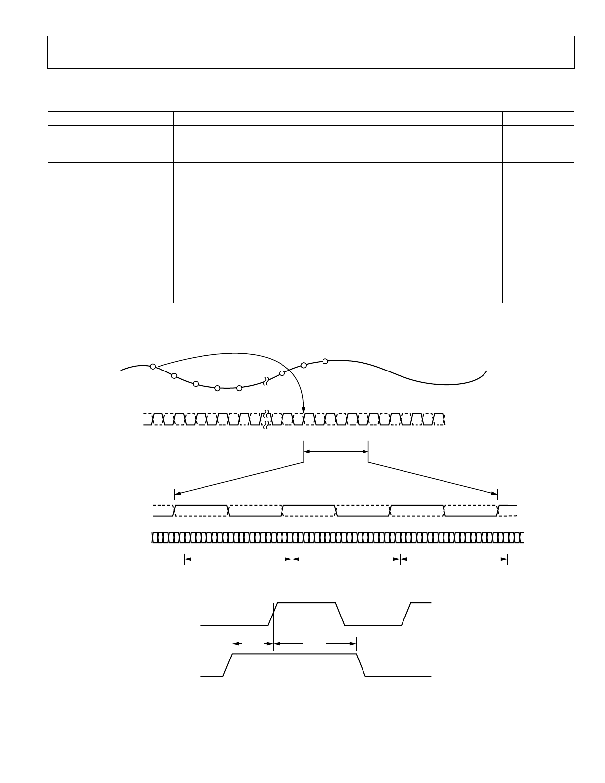
Figure 2. Data Output Timing
CLK+
t
HSYNC
09180-004
SYNC
t
SSYNC
Figure 3. SYNC Input Timing Requirements
Rev. B | Page 9 of 44
Page 10

AD9644
ABSOLUTE MAXIMUM RATINGS
Table 6.
Parameter Rating
ELECTRICAL
AVDD to AGND −0.3 V to +2.0 V
DRVDD to AGND −0.3 V to +2.0V
VIN+A/VIN+B, VIN−A/VIN−B to AGND −0.3 V to AVDD + 0.2 V
CLK+, CLK− to AGND −0.3 V to AVDD + 0.2 V
SYNC to AGND −0.3 V to AVDD + 0.2 V
VCMA, VCMB to AGND −0.3 V to AVDD + 0.2 V
CSB to AGND −0.3 V to DRVDD + 0.2 V
SCLK to AGND −0.3 V to DRVDD + 0.2 V
SDIO to AGND −0.3 V to DRVDD + 0.2 V
PDWN to AGND −0.3 V to DRVDD + 0.2 V
DOUT+A, DOUT0−A, DOUT0+B,
DOUT−B to AGND
DSYNC+A, DSYNC−A, DSYNC+B,
DSYNC−B to AGND
−0.3 V to DRVDD + 0.2 V
−0.3 V to DRVDD + 0.2 V
ENVIRONMENTAL
Operating Temperature Range
−40°C to +85°C
(Ambient)
Maximum Junction Temperature
150°C
Under Bias
Storage Temperature Range
−65°C to +150°C
(Ambient)
Stresses above those listed under Absolute Maximum Ratings
may cause permanent damage to the device. This is a stress
rating only; functional operation of the device at these or any
other conditions above those indicated in the operational
section of this specification is not implied. Exposure to absolute
maximum rating conditions for extended periods may affect
device reliability.
THERMAL CHARACTERISTICS
The exposed paddle must be soldered to the ground plane for
the LFCSP package. Soldering the exposed paddle to the PCB
increases the reliability of the solder joints and maximizes the
thermal capability of the package.
Table 7. Thermal Resistance
Airflow
Veloc ity
Packa ge Type
48-Lead LFCSP
7 mm × 7 mm
(CP-48-8)
1
Per JEDEC 51-7, plus JEDEC 25-5 2S2P test board.
2
Per JEDEC JESD51-2 (still air) or JEDEC JESD51-6 (moving air).
3
Per MIL-STD 883, Method 1012.1.
4
Per JEDEC JESD51-8 (still air).
(m/sec) θ
0 25 2 14 °C/W
1.0 22 °C/W
2.5 20 °C/W
1, 2
JA
1, 3
θ
JC
1, 4
θ
Unit
JB
Typical θJA is specified for a 4-layer PCB with a solid ground
plane. As shown Tabl e 7, airflow improves heat dissipation,
which reduces θ
. In addition, metal in direct contact with the
JA
package leads from metal traces, through holes, ground, and
power planes, reduces θ
.
JA
ESD CAUTION
Rev. B | Page 10 of 44
Page 11
AD9644
B
A
A
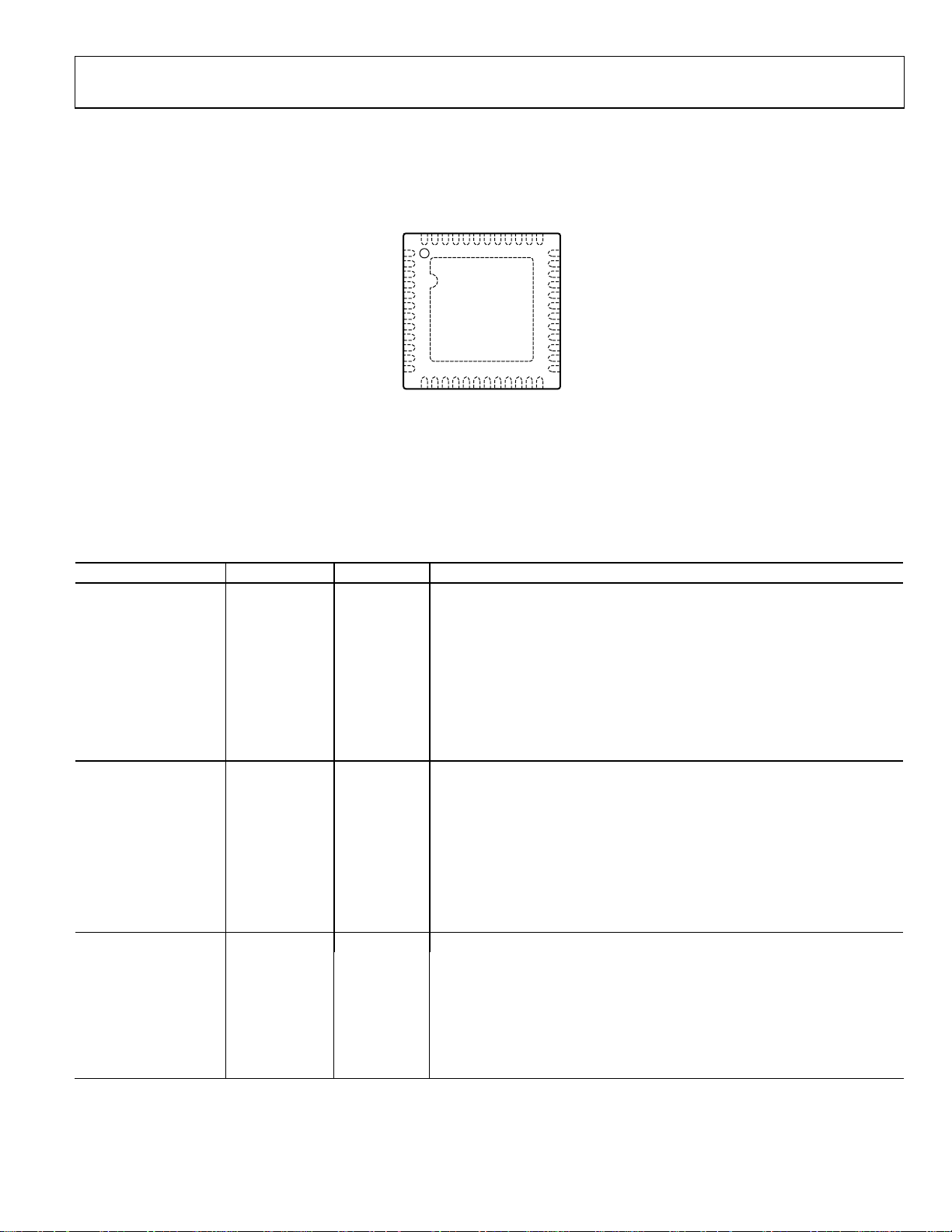
PIN CONFIGURATION AND FUNCTION DESCRIPTIONS
D
AVDD
84
AVDD
AVDD
74
AVDD
VIN–B
VIN+
AVD
64
54
44
VIN–
AVDD
AVDD
AVDD
VIN+
93
14
34
24
73
83
04
1
VCMB
2
AVDD
3
DNC
4
AVDD
5
CLK+
6
CLK–
7
AVDD
8
SYNC
9
AVDD
10
DRGND
11
DRVDD
12
DNC
NOTES
1. DNC = DO NOT CO NNECT.
2. THE EXPO SED THERMAL PAD ON THE BOTTOM OF THE PACKAGE
PROVIDES THE ANALOG GROUND FOR THE PART. THIS EXPOSED PAD
MUST BE CONNECTED TO GROUND FOR PROPER OPERATION.
51
41
31
DRVDD
DSYNC–B
DSYNC+B
AD9644
TOP
VIEW
(Not to Scale)
91
81
71
61
DRGND
DOUT–A
DOUT–B
DOUT+B
32
22
12
02
DRVDD
DRGND
DOUT+A
DSYNC–A
VCMA
36
DNC
35
DNC
34
PDWN
33
32
DNC
CSB
31
SCLK
30
SDIO
29
28
DRVDD
27
DRVDD
DRGND
26
25
DNC
42
DSYNC+A
09180-104
Figure 4. LFCSP Pin Configuration (Top View)
Table 8. Pin Function Descriptions
Pin No. Mnemonic Type Description
ADC Power Supplies
11, 15, 22, 27, 28 DRVDD Supply Digital Output Driver Supply (1.8 V Nominal).
2, 4, 7, 9, 37, 38, 41,
AVDD Supply Analog Power Supply (1.8 V Nominal).
42, 43, 44, 47, 48
3, 12, 25, 32, 34, 35 DNC Do Not Connect.
10, 16, 21, 26 DRGND
Driver
Digital Driver Supply Ground.
Ground
0
AGND,
Exposed Pad
Ground
The exposed thermal pad on the bottom of the package provides the analog
ground for the part. This exposed pad must be connected to ground for
proper operation.
ADC Analog
40 VIN+A Input Differential Analog Input Pin (+) for Channel A.
39 VIN−A Input Differential Analog Input Pin (−) for Channel A.
45 VIN+B Input Differential Analog Input Pin (+) for Channel B.
46 VIN−B Input Differential Analog Input Pin (−) for Channel B.
36 VCMA Output Common-Mode Level Bias Output for Channel A Analog Input.
1 VCMB Output Common-Mode Level Bias Output for Channel B Analog Input.
5 CLK+ Input ADC Clock Input—True.
6 CLK− Input ADC Clock Input—Complement.
Digital Input
8 SYNC Input Input Clock Divider Synchronization Pin.
24 DSYNC+A Input
Active Low JESD204A LVDS Channel A SYNC Input—True/JESD204A CMOS
Channel A SYNC Input.
23 DSYNC−A Input Active Low JESD204A LVDS Channel A SYNC Input—Complement.
14 DSYNC+B Input
Active Low JESD204A LVDS Channel B SYNC Input—True/JESD204A CMOS
Channel A SYNC Input.
13 DSYNC−B Input Active Low JESD204A LVDS Channel B SYNC Input—Complement.
Rev. B | Page 11 of 44
Page 12

AD9644
Pin No. Mnemonic Type Description
Digital Outputs
20 DOUT+A Output Channel A CML Output Data—True.
19 DOUT−A Output Channel A CML Output Data—Complement.
18 DOUT+B Output Channel B CML Output Data—True.
17 DOUT−B Output Channel B CML Output Data—Complement.
SPI Control
30 SCLK Input SPI Serial Clock.
29 SDIO Input/Output SPI Serial Data Input/Output.
31 CSB Input SPI Chip Select (Active Low).
ADC Configuration
33 PDWN Input
Power-Down Input. Using the SPI interface, this input can be configured as
power-down or standby.
Rev. B | Page 12 of 44
Page 13
AD9644
TYPICAL PERFORMANCE CHARACTERISTICS
AVDD = 1.8 V, DRVDD = 1.8 V, DCS enabled, 1.75 V p-p differential input, VIN = −1.0 dBFS, and 32k sample,
T
= 25°C, unless otherwise noted.
A
–20
–40
0
80MSPS
10.1MHz @ –1dBFS
SNR = 73.0dB ( 74.0dBFS)
SFDR = 95dBc
0
80MSPS
140.3MHz @ –1dBF S
–20
SNR = 72.2dB (73.2dBFS)
SFDR = 94.0dBc
–40
–60
–80
AMPLITUDE (dBFS)
–100
–120
–140
0 102030
THIRD HARMONIC
FREQUENCY (M Hz)
Figure 5. AD9644-80 Single-Tone FFT with f
0
80MSPS
30.1MHz @ –1dBFS
–20
SNR = 72.7dB (73.7dBFS)
SFDR = 94dBc
–40
–60
–80
AMPLITUDE (dBFS)
THIRD HARMONI C
–100
–120
–140
0 102030
SECOND HARMONIC
FREQUENCY (M Hz)
Figure 6. AD9644-80 Single-Tone FFT with f
0
–20
–40
80MSPS
70.1MHz @ –1dBF S
SNR = 72.5dB (73.5dBFS)
SFDR = 94.0dBc
= 10.1 MHz
IN
= 30.1 MHz
IN
40
09180-005
40
09180-106
–60
–80
AMPLITUDE (dBFS)
–100
–120
–140
0 102030
Figure 8. AD9644-80 Single-Tone FFT with f
0
80MSPS
180.1MHz @ –1dBF S
–20
SNR = 71.6dB (72.6dBFS)
SFDR = 93dBc
–40
–60
–80
AMPLITUDE (dBFS)
–100
–120
–140
0 1020304
Figure 9. AD9644-80 Single-Tone FFT with f
0
80MSPS
220.1MHz @ –1dBF S
–20
SNR = 71.1dB (72.1dBFS)
SFDR = 92dBc
–40
FREQUENCY (M Hz)
FREQUENCY (M Hz)
= 140.1 MHz
IN
SECOND HARMONI C
= 180.1 MHz
IN
40
09180-108
0
09180-109
–60
–80
AMPLITUDE (dBFS)
–100
–120
–140
0 102030
SECOND HARMONI C
THIRD HARMONI C
FREQUENCY (M Hz)
Figure 7. AD9644-80 Single-Tone FFT with f
= 70.1 MHz
IN
40
09180-107
Rev. B | Page 13 of 44
–60
THIRD HARMONI C
–80
AMPLITUDE (dBFS)
–100
–120
–140
0 102030
FREQUENCY (M Hz)
SECOND HARMONI C
Figure 10. AD9644-80 Single-Tone FFT with f
= 220.1 MHz
IN
40
09180-110
Page 14
AD9644
120
100
100
80
60
40
SNR/SFDR (d Bc/dBFS)
20
SFDR (dBFS)
SFDR (dBc)
SNR (dBFS)
SNR (dBc)
0
–100
–95
–90
–85
–80
–75
–70
–65
–60
–55
–50
–45
–40
–35
–30
INPUT AMPLITUDE (dBFS)
–25
–5
–20
–15
–10
Figure 11. AD9644-80 Single-Tone SNR/SFDR vs. Input Amplitude (A
= 10.1 MHz, fS = 80 MSPS
with f
IN
120
100
80
SFDR (dBFS)
60
SFDR (dBc)
SNR (dBFS)
SNR (dBc)
40
SNR/SFDR (dBc/dBFS)
20
95
90
85
80
SNR/SFDR (dBFS/dBc)
75
70
0
09180-111
)
IN
65
Figure 14. AD9644-80 Single-Tone SNR/SFDR vs. Input Frequency (f
–20
–40
–60
–80
SFDR/IMD3 (dBc/dBFS )
–100
SNR @ –40°C
SFDR @ –40°C
SNR @ +25°C
SFDR @ +25°C
SNR @ +85°C
SFDR @ +85°C
0 50 100 150 200 250
Temperature with 2.0 V p-p Full-Scale, f
0
SFDR (dBc)
IMD3 (d Bc)
SFDR (dBFS)
IMD3 (d BFS)
INPUT FREQUENCY (MHz)
= 80 MSPS
S
) and
IN
09180-114
0
–95
–90
–85
–80
–75
–70
–65
–60
–55
–50
–45
–40
–35
–30
–100
INPUT AMPLITUDE (dBFS)
–25
–5
–20
–15
–10
Figure 12. AD9644-80 Single-Tone SNR/SFDR vs. Input Amplitude (A
with f
= 180 MHz, fS = 80 MSPS
IN
100
95
90
85
80
SNR/SFDR (dBFS/dBc)
75
70
65
SNR @ –40°C
SFDR @ –40°C
SNR @ +25°C
SFDR @ +25°C
SNR @ +85°C
SFDR @ +85°C
0 50 100 150 200 250
INPUT FREQUENCY (MHz)
Figure 13. AD9644-80 Single-Tone SNR/SFDR vs. Input Frequency (f
Temperature with 1.75 V p-p Full-Scale, f
= 80 MSPS
S
0
) and
IN
–120
–90 –78 –66 –54 –42 –30 –18 –6
9180-112
)
IN
Figure 15. AD9644-80 Two-Tone SFDR/IMD3 vs. Input Amplitude (A
with f
0
–20
–40
–60
–80
SFDR/IMD3 ( dBc/dBFS)
–100
–120
09180-113
SFDR (dBc)
IMD3 (dBc)
SFDR (dBFS)
IMD3 (dBFS)
–90 –78 –66 –54 –42 –30 –18 –6
Figure 16. AD9644-80 Two-Tone SFDR/IMD3 vs. Input Amplitude (A
with f
IN1
INPUT AMPLITUDE (dBFS)
= 29.9 MHz, f
IN1
INPUT AMPLITUDE (dBFS)
= 169.1 MHz, f
= 32.9 MHz, fS = 80 MSPS
IN2
= 172.1 MHz, fS = 80 MSPS
IN2
09180-015
)
IN
09180-116
)
IN
Rev. B | Page 14 of 44
Page 15

AD9644
0
80MSPS
29.9MHz @ –7dBFS
–20
32.9MHz @ –7dBFS
SFDR = 94.4d Bc (101.4dBFS)
–40
14,000
12,000
10,000
–60
–80
AMPLITUDE (dBFS)
–100
–120
–140
0 102030
Figure 17. AD9644-80 Two-Tone FFT with f
0
–20
–40
–60
–80
AMPLITUDE (dBFS)
–100
–120
–140
0 102030
FREQUENCY (M Hz)
= 29.9 MHz and f
IN1
80MSPS
169.1MHz @ –7dBF S
172.1MHz @ –7dBF S
SFDR = 91.9d Bc (98.9dBF S)
FREQUENCY (M Hz)
Figure 18. AD9644-80 Two-Tone FFT with f
= 172.1 MHz
f
IN2
100
IN2
= 169.1 MHz and
IN1
40
= 32.9 MHz
40
8000
6000
NUMBER OF HITS
4000
2000
0
N – 4 N – 3 N – 2 N – 1 N N + 1 N + 2 N + 3 N + 4
09180-117
OUTPUT CO DE
09180-020
Figure 20. AD9644-80 Grounded Input Histogram
1.0
0.8
0.6
0.4
0.2
0
–0.2
INL ERROR (L SB)
–0.4
–0.6
–0.8
–1.0
0 200 400 600 800 1000 1200 1400 1600
09180-118
Figure 21. AD9644-80 INL with f
OUTPUT CODE
= 30.3 MHz
IN
09180-121
0.50
95
90
SNR CHANNEL B
85
80
SNR/SFDR (dBFS/dBc)
75
70
SFDR CHANNEL B
SNR CHANNEL A
SFDR CHANNEL A
45 50 55 60 65 70 75 80
SAMPLE RATE (MSPS)
Figure 19. AD9644-80 Single-Tone SNR/SFDR vs. Sample Rate (f
= 70. MHz
with f
IN
09180-119
)
S
Rev. B | Page 15 of 44
0.25
0
DNL ERROR (LSB)
–0.25
–0.50
0 2000 4000 6000 8000 10,000 12,000 14,000 16,000
Figure 22. AD9644-80 DNL with f
OUTPUT CODE
= 30.3 MHz
IN
09180-122
Page 16

AD9644
AMPLIT UDE (dBFS)
–20
–40
–60
–80
–100
0
THIRD HARMO NIC
155MSPS
10.1MHz @ –1d BFS
SNR = 70.9dB (71.9dBFS)
SFDR = 94dBc
AMPLIT UDE (dBFS)
–20
–40
–60
–80
–100
0
SECOND HARMO NIC
155MSPS
140.1MHz @ –1d BFS
SNR = 70.5dB (71.5dBFS)
SFDR = 92dBc
THIRD HARMO NIC
–120
–140
0 7.75 15.50 23.25 31.00 38.75 46. 50 54.25 62.00 69. 75 77. 50
Figure 23. AD9644-155 Single-Tone FFT with f
FREQUENCY (MHz)
= 10.1 MHz
IN
0
–20
–40
–60
–80
AMPLIT UDE (dBFS)
–100
–120
–140
0 7.75 15.50 23.25 31.00 38.75 46. 50 54.25 62.00 69. 75 77. 50
FREQUENCY (MHz)
Figure 24. AD9644-155 Single-Tone FFT with f
155MSPS
30.1MHz @ –1d BFS
SNR = 70.8dB (71.8dBFS)
SFDR = 93dBc
SECOND
HARMONIC
HARMONIC
= 30.1 MHz
IN
0
155MSPS
70.1MHz @ –1dBFS
–20
SNR = 70.7dB (71.7dBF S)
SFDR = 92dBc
–40
THIRD
–120
–140
0 7.75 15.50 23.25 31.00 38.75 46. 50 54.25 62.00 69. 75 77. 50
09180-123
Figure 26. AD9644-155 Single-Tone FFT with f
FREQUENCY (MHz)
= 140.1 MHz
IN
09180-126
0
–20
–40
–60
–80
AMPLIT UDE (dBFS)
–100
–120
–140
0 7.75 15.50 23.25 31.00 38.75 46. 50 54.25 62.00 69. 75 77. 50
09180-124
FREQUENCY (MHz)
Figure 27. AD9644-155 Single-Tone FFT with f
155MSPS
180.1MHz @ –1d BFS
SNR = 70.4dB (71.4dBFS)
SFDR = 92dBc
THIRD HARMO NIC
= 180.1 MHz
IN
09180-127
0
155MSPS
220.1MHz @ –1dBFS
–20
SNR = 70.0dB (71.0dBFS)
SFDR = 90dBc
–40
–60
–80
AMPLIT UDE (dBFS)
–100
–120
–140
0 7.75 15.50 23.25 31.00 38.75 46. 50 54.25 62.00 69. 75 77. 50
Figure 25. AD9644-155 Single-Tone FFT with f
FREQUENCY (MHz)
= 70.1 MHz
IN
09180-125
Rev. B | Page 16 of 44
–60
–80
AMPLIT UDE (dBFS)
–100
–120
–140
0 7.75 15.50 23.25 31.00 38.75 46. 50 54.25 62.00 69. 75 77. 50
Figure 28. AD9644-155 Single-Tone FFT with f
THIRD HARMO NIC
FREQUENCY (MHz)
= 220.1 MHz
IN
09180-128
Page 17

AD9644
120
SFDR (dBFS)
100
80
60
40
SNR/SFDR (dBc AND dBFS)
20
0
–90 –80 –70 –60 –50 –40 –30 –20 –10 0
SNR (dBFS)
SFDR (dBc)
SNR (dBc)
INPUT AMPLITUDE (dBFS)
Figure 29. AD9644-155 Single-Tone SNR/SFDR vs. Input Amplitude (A
= 10.1 MHz, fS = 80 MSPS
with f
IN
120
SFDR (d BFS)
100
80
60
40
SNR/SFDR (dBc AND dBFS)
20
0
–90 –80 –70 –60 –50 –40 –30 –20 –10 0
SNR (dBFS)
SFDR (dBc)
SNR (dBc)
INPUT AMPLITUDE (dBFS)
Figure 30. AD9644-155 Single-Tone SNR/SFDR vs. Input Amplitude (A
= 180 MHz, fS = 80 MSPS
with f
IN
100
100
95
90
85
80
75
SNR/SFDR (d BFS/dBc)
70
65
09180-129
)
IN
0 50 100 150 200 250 300
Figure 32. AD9644-155 Single-Tone SNR/SFDR vs. Input Frequency (f
INPUT FREQUENCY (MHz)
Temperature with 2.0 V p-p Full-Scale, f
0
–20
–40
SFDR (dBc)
–60
–80
SFDR/IMD3 (d Bc AND dBFS)
–100
–120
09180-130
)
IN
–90 –78 –66 –54 –42 –30 –18 –6
Figure 33. AD9644-155 Two-Tone SFDR/IMD3 vs. Input Amplitude (A
= 29.9 MHz, f
with f
IN1
0
IMD3 (dBc)
SFDR (d BFS)
IMD3 (dBFS)
INPUT AMPLITUDE (dBFS)
= 32.9 MHz, fS = 80 MSPS
IN2
SNR @ –40°C
SFDR @ –40°C
SNR @ +25°C
SFDR @ +25°C
SNR @ +85°C
SFDR @ +85°C
= 80 MSPS
S
) and
IN
09180-132
09180-133
)
IN
95
90
SNR @ –40°C
SFDR @ –40°C
85
SNR @ +25°C
SFDR @ +25°C
SNR @ +85°C
80
SFDR @ +85°C
75
SNR/SFDR (d BFS/dBc)
70
65
0 50 100 150 200 250 300
INPUT FREQUENCY (MHz)
Figure 31. AD9644-155 Single-Tone SNR/SFDR vs. Input Frequency (f
Temperature with 1.75 V p-p Full-Scale, f
= 80 MSPS
S
09180-131
) and
IN
Rev. B | Page 17 of 44
–20
–40
–60
–80
SFDR/IMD3 (d Bc AND dBFS)
–100
–120
IMD3 (dBFS)
–90 –78 –66 –54 –42 –30 –18 –6
INPUT AMPLITUDE (dBFS)
SFDR (d Bc)
IMD3 (dBc)
SFDR (d BFS)
Figure 34. AD9644-155 Two-Tone SFDR/IMD3 vs. Input Amplitude (A
with f
= 169.1 MHz, f
IN1
= 172.1 MHz, fS = 80 MSPS
IN2
09180-134
)
IN
Page 18

AD9644
AMPLIT UDE (dBFS)
–20
–40
–60
–80
–100
–120
0
155MSPS
29.9MHz @ –7dBFS
32.9MHz @ –7dBFS
SFDR = 89.8dBc (96.8dBFS)
NUMBER OF HI TS
4000
3500
3000
2500
2000
1500
1000
500
–140
0 7.75 15.50 23.25 31.00 38.75 46.50 54. 25 62.00 69.75 77.50
Figure 35. AD9644-155 Two-Tone FFT with f
FREQUENCY (MHz)
= 29.9 MHz and f
IN1
0
–20
–40
–60
–80
AMPLIT UDE (dBFS)
–100
–120
–140
0 7.75 15.50 23.25 31.00 38.75 46.50 54. 25 62.00 69.75 77.50
FREQUENCY (MHz)
155MSPS
169.1MHz @ –7dBFS
172.1MHz @ –7dBFS
SFDR = 89.1dBc (96.1dBFS)
Figure 36. AD9644-155 Two-Tone FFT with f
= 172.1 MHz
f
IN2
100
95
90
IN2
= 169.1 MHz and
IN1
09180-135
= 32.9 MHz
09180-136
0
N – 5N – 4N – 3N – 2N – 1 N N + 1N + 2N + 3N + 4N + 5
OUTPUT CODE
Figure 38. AD9644-155 Grounded Input Histogram
1
0.8
0.6
0.4
0.2
0
–0.2
INL ERROR (LSB)
–0.4
–0.6
–0.8
–1
0 2000 4000 6000 8000 10000 12000 14000 16000
Figure 39. AD9644-155 INL with f
OUTPUT CO DE
= 30.3 MHz
IN
0.5
0.25
09180-138
09180-139
85
SNR, CHANNEL B
80
SNR/SF DR (dBFS /dBc
75
70
50 65 80 95 110 125 140 155
SAMPLE RATE (MSPS)
SFDR, CHANNEL B
SNR, CHANNEL A
SFDR, CHANNEL A
Figure 37. AD9644-155 Single-Tone SNR/SFDR vs. Sample Rate (f
with f
= 70. MHz
IN
09180-137
)
S
Rev. B | Page 18 of 44
0
DNL ERROR (LSB)
–0.25
–0.5
0 2000 4000 6000 8000 10000 12000 14000 16000
Figure 40. AD9644-155 DNL with f
OUTPUT CODE
= 30.3 MHz
IN
09180-140
Page 19

AD9644
V
C
A
EQUIVALENT CIRCUITS
AVDD
SCLK
IN
OR
PDWN
350Ω
30kΩ
Figure 41. Equivalent Analog Input Circuit
AVDD
AVDD AVDD
LK+
0.9V
15kΩ 15kΩ
Figure 42. Equivalent Clock Input Circuit
DRVDD
4mA
DOUT±A/B DOUT±A/ B
4mA
R
TERM
V
CM
4mA
4mA
Figure 43. Digital CML Output
09180-008
09180-012
Figure 45. Equivalent SCLK or PDWN Input Circuit
AVDD
30kΩ
350Ω
09180-014
CLK–
CSB
09180-009
Figure 46. Equivalent CSB Input Circuit
VDD AVDD
DSYNC ±A/ B
OR SYNC
16kΩ
0.9V
09180-089
0.9V
09180-025
Figure 47. Equivalent SYNC and DSYNC Input Circuit
SDIO
DRVDD
30kΩ
350Ω
09180-011
Figure 44. Equivalent SDIO Circuit
Rev. B | Page 19 of 44
Page 20

AD9644
V
V
THEORY OF OPERATION
The AD9644 dual-core analog-to-digital converter (ADC) can
be used for diversity reception of signals, in which the ADCs are
operating identically on the same carrier but from two separate
antennae. The ADCs can also be operated with independent
analog inputs. The user can sample any f
/2 frequency segment
S
from dc to 250 MHz, using appropriate low-pass or band-pass
filtering at the ADC inputs with little loss in ADC performance.
In nondiversity applications, the AD9644 can be used as a baseband or direct downconversion receiver, in which one ADC is
used for I input data, and the other is used for Q input data.
Synchronization capability is provided to allow synchronized
timing between multiple devices.
Programming and control of the AD9644 are accomplished
using a 3-wire SPI-compatible serial interface.
ADC ARCHITECTURE
The AD9644 architecture consists of a dual front-end sampleand-hold circuit, followed by a pipelined, switched-capacitor
ADC. The quantized outputs from each stage are combined into
a final 14-bit result in the digital correction logic. The pipelined
architecture permits the first stage to operate on a new input
sample and the remaining stages to operate on the preceding
samples. Sampling occurs on the rising edge of the clock.
Each stage of the pipeline, excluding the last, consists of a low
resolution flash ADC connected to a switched-capacitor digitalto-analog converter (DAC) and an interstage residue amplifier
(MDAC). The MDAC magnifies the difference between the reconstructed DAC output and the flash input for the next stage in
the pipeline. One bit of redundancy is used in each stage to
facilitate digital correction of flash errors. The last stage simply
consists of a flash ADC.
The input stage of each channel contains a differential sampling
circuit that can be ac- or dc-coupled in differential or singleended modes. The output staging block aligns the data, corrects
errors, and passes the data to the output buffers. The output buffers
are powered from a separate supply, allowing digital output noise to
be separated from the analog core. During power-down, the
output buffers go into a high impedance state.
ANALOG INPUT CONSIDERATIONS
The analog input to the AD9644 is a differential switchedcapacitor circuit that has been designed for optimum performance
while processing a differential input signal.
The clock signal alternatively switches the input between sample
mode and hold mode (see Figure 48). When the input is switched
into sample mode, the signal source must be capable of charging
the sample capacitors and settling within ½ of a clock cycle.
A small resistor in series with each input can help reduce the
peak transient current required from the output stage of the
driving source. A shunt capacitor can be placed across the
inputs to provide dynamic charging currents. This passive
network creates a low-pass filter at the ADC input; therefore,
the precise values are dependent on the application.
In intermediate frequency (IF) undersampling applications, any
shunt capacitors or series resistors should be reduced since the
input sample capacitor is unbuffered. In combination with the
driving source impedance, the shunt capacitors limit the input
bandwidth. Refer to the AN-742 Application Note, Frequency
Domain Response of Switched-Capacitor ADCs; the AN-827
Application Note, A Resonant Approach to Interfacing Amplifiers to
Switched-Capacitor ADCs; and the Analog Dialog article,
“Transformer-Coupled Front-End for Wideband A/D Converters,”
for more information on this subject (refer to www.analog.com).
BIAS
IN+
IN–
S
C
S
C
PAR1
C
PAR1
C
PAR2
H
C
S
C
PAR2
S
Figure 48. Switched-Capacitor Input
BIAS
S
C
FB
S
C
S
FB
S
For best dynamic performance, the source impedances driving
VIN+ and VIN− should be matched, and the inputs should be
differentially balanced.
Input Common Mode
The analog inputs of the AD9644 are not internally dc biased.
In ac-coupled applications, the user must provide this bias
externally. Setting the device so that VCM = 0.5 × AVDD (or
0.9 V) is recommended for optimum performance. An onboard common-mode voltage reference is included in the
design and is available from the VCMA and VCMB pins. Using
the VCMA and VCMB outputs to set the input common mode
is recommended. Optimum performance is achieved when the
common-mode voltage of the analog input is set by the VCMA
and VCMB pin voltages (typically 0.5 × AVDD). The VCMA
and VCMB pins must be decoupled to ground by a 0.1 µF
capacitor. This decoupling capacitor should be placed close
to the pin to minimize the series resistance and inductance
between the part and this capacitor.
09180-034
Rev. B | Page 20 of 44
Page 21

AD9644
V
F
2
p
Differential Input Configurations
Optimum performance is achieved while driving the AD9644 in a
differential input configuration. For baseband applications, the
AD8138, ADA4937-2, and ADA4938-2 differential drivers provide
excellent performance and a flexible interface to the ADC.
The output common-mode voltage of the ADA4938-2 is easily
set with the VCM pin of the AD9644 (see Figure 49), and the
driver can be configured in a Sallen-Key filter topology to provide
band limiting of the input signal.
15p
200Ω
76.8Ω
IN
0.1µF
90Ω
ADA4938-2
120Ω
200Ω
33Ω
33Ω
5pF
15pF
15Ω
15Ω
VIN–
VIN+
AVDD
ADC
VCM
Figure 49. Differential Input Configuration Using the ADA4938-2
For baseband applications in which SNR is a key parameter,
differential transformer coupling is the recommended input
configuration. An example is shown in Figure 50. To bias the
analog input, the VCM voltage can be connected to the center
tap of the secondary winding of the transformer.
C2
R3
R2
R1
2V p-p
49.9Ω
0.1µF
C1
R1
R3
C2
Figure 50. Differential Transformer-Coupled Configuration
VIN+
ADC
R2
VIN–
VCM
09180-039
09180-040
The signal characteristics must be considered when selecting
a transformer. Most RF transformers saturate at frequencies
below a few megahertz (MHz). Excessive signal power can also
cause core saturation, which leads to distortion.
At input frequencies in the second Nyquist zone and above, the
noise performance of most amplifiers is not adequate to achieve
the true SNR performance of the AD9644. For applications in
which SNR is a key parameter, differential double balun coupling
is the recommended input configuration (see Figure 51). In this
configuration, the input is ac-coupled and the VCM is provided
to each input through a 33 Ω resistor. These resistors compensate
for losses in the input baluns to provide a 50 Ω impedance to
the driver.
In the double balun and transformer configurations, the value of
the input capacitors and resistors is dependent on the input frequency and source impedance. Based on these parameters the
value of the input resistors and capacitors may need to be
adjusted or some components may need to be removed. Tabl e 9
displays recommended values to set the RC network for different
input frequency ranges. However, these values are dependent on
the input signal and bandwidth and should be used only as a
starting guide. Note that the values given in Tab l e 9 are for each
R1, R2, C2, and R3 component shown in Figure 50 and Figure 51.
Table 9. Example RC Network
Frequency
Range
(MHz)
R1
Series
(Ω)
C1
Differential
(pF)
R2
Series
(Ω)
C2
Shunt
(pF)
0 to 100 33 8.2 0 8.2 49.9
100 to 250 15 3.9 0 Open Open
R3
Shunt
(Ω)
An alternative to using a transformer-coupled input at frequencies
in the second Nyquist zone is to use the AD8376 variable gain
amplifier. An example drive circuit including a band-pass filter
is shown in Figure 52. See the AD8376 data sheet for more
information.
C2
R3
R1
C1
R1R2R2
R3
C2
VIN+
VIN–
ADC
VCM
09180-041
V p-
0.1µF
0.1µF
0.1µF
33Ω
33Ω
0.1µF
SP
A
P
S
Figure 51. Differential Double Balun Input Configuration
Rev. B | Page 21 of 44
Page 22

AD9644
F
C
1µH
AD8376
1µH
NOTES
1. ALL INDUCTORS ARE COIL CRAFT 0603CS COMPONENTS
WITH T HE EXCEPTI ON OF T HE 1µH CHOKE INDU
VPOS
1nF
1000pF
180nH1000p
301Ω
180nH
Figure 52. Differential Input Configuration Using the AD8376 (Filter Values Shown Are for a 20 MHz Bandwidth Filter Centered at 140 MHz)
VOLTAGE REFERENCE
A stable and accurate voltage reference is built into the AD9644.
The input full scale range can be adjusted through the SPI port by
adjusting Bit 0 through Bit 4 of Register 0x18. These bits can be
used to change the full scale between 1.383 V p-p and 2.087 V p-p
in 0.022 V steps, as shown in Tab l e 1 7 .
CLOCK INPUT CONSIDERATIONS
For optimum performance, the AD9644 sample clock inputs,
CLK+ and CLK−, should be clocked with a differential signal.
The signal is typically ac-coupled into the CLK+ and CLK− pins by
means of a transformer or a passive component configuration.
These pins are biased internally (see Figure 53) and require no
external bias. If the inputs are floated, the CLK− pin is pulled low
to prevent inadvertent clocking.
AVDD
220nH
165Ω
5.1pF 3.9pF
165Ω
220nH
15pF
VCM
1nF
68nH
AD9644
TORS (0603LS).
09180-115
secondary limit clock excursions into the AD9644 to
approximately 0.8 V p-p differential.
This limit helps prevent the large voltage swings of the clock
from feeding through to other portions of the AD9644 while
preserving the fast rise and fall times of the signal that are critical
to a low jitter performance.
XFMR
0.1µF
®
0.1µF0.1µF
0.1µF
SCHOTTKY
DIODES:
HSMS2822
ADC
CLK+
CLK–
Mini-Circuits
ADT1-1W T, 1:1 Z
CLOCK
INPUT
50Ω
100Ω
Figure 54. Transformer-Coupled Differential Clock (Up to 200 MHz)
9180-048
0.9V
CLK+
CLK–
2pF2pF
9180-044
Figure 53. Equivalent Clock Input Circuit
Clock Input Options
The AD9644 has a very flexible clock input structure. Clock input
can be a CMOS, LVDS, LVPECL , or s i n e w ave sig n a l . R egard less of
the type of signal being used, clock source jitter is of the most
concern, as described in the Jitter Considerations section. The
minimum conversion rate of the AD9644 is 40 MSPS. At clock
rates below 40 MSPS, dynamic performance of the AD9644 can
degrade.
Figure 54 and Figure 55 show two preferred methods for clocking
the AD9644 (at clock rates up to 640 MHz). A low jitter clock
source is converted from a single-ended signal to a differential
signal using either an RF balun or an RF transformer.
The RF balun configuration is recommended for clock frequencies
between 125 MHz and 640 MHz, and the RF transformer is recommended for clock frequencies from 40 MHz to 200 MHz. The
back-to-back Schottky diodes across the transformer/balun
ADC
CLOCK
INPUT
50Ω
1nF
0.1µF1nF
0.1µF
SCHOTTKY
DIODES:
HSMS2822
CLK+
CLK–
09180-049
Figure 55. Balun-Coupled Differential Clock (Up to 640 MHz)
If a low jitter clock source is not available, another option is to
ac couple a differential PECL signal to the sample clock input
pins, as shown in Figure 56. The AD9510/AD9511/AD9512/
AD9513/AD9514/AD9515/AD9516/AD9517/AD9518/AD9520
/AD9522 clock drivers offer excellent jitter performance.
240Ω240Ω
0.1µF0.1µF
0.1µF
100Ω
CLK+
ADC
CLK–
CLOCK
INPUT
CLOCK
INPUT
AD95xx
PECL DRIVER
0.1µF
50kΩ 50kΩ
Figure 56. Differential PECL Sample Clock (Up to 640 MHz)
09180-050
Rev. B | Page 22 of 44
Page 23

AD9644
A third option is to ac-couple a differential LVDS signal to the
sample clock input pins, as shown in Figure 57. The AD9510/
AD9511/AD9512/AD9513/AD9514/AD9515/AD9516/AD9517/
AD9518/AD9520/AD9522 clock drivers offer excellent jitter
performance.
CLOCK
INPUT
CLOCK
INPUT
0.1µF
AD95xx
LVDS DRIVER
0.1µF
50kΩ 50kΩ
Figure 57. Differential LVDS Sample Clock (Up to 640 MHz)
0.1µF
100Ω
0.1µF
CLK+
ADC
CLK–
In some applications, it may be acceptable to drive the sample
clock inputs with a single-ended CMOS signal. In such applications, the CLK+ pin should be driven directly from a CMOS gate,
and the CLK− pin should be bypassed to ground with a 0.1 F
capacitor (see Figure 58).
V
CC
0.1µF
CLOCK
INPUT
1
50Ω RESISTOR IS OPTIONAL.
50Ω
1kΩ
1
1kΩ
AD95xx
CMOS DRIVER
OPTIO NAL
100Ω
0.1µF
0.1µF
CLK+
ADC
CLK–
Figure 58. Single-Ended 1.8 V CMOS Input Clock (Up to 200 MHz)
Input Clock Divider
The AD9644 contains an input clock divider with the ability to
divide the input clock by integer values between 1 and 8. For
divide ratios other than 1 the duty cycle stabilizer is automatically
enabled.
The AD9644 clock divider can be synchronized using the external
SYNC input. Bit 1 and Bit 2 of Register 0x3A allow the clock
divider to be resynchronized on every SYNC signal or only on
the first SYNC signal after the register is written. A valid SYNC
causes the clock divider to reset to its initial state. This synchronization feature allows multiple parts to have their clock dividers
aligned to guarantee simultaneous input sampling.
Clock Duty Cycle
Typical high speed ADCs use both clock edges to generate
a variety of internal timing signals and, as a result, may be
sensitive to clock duty cycle. The AD9644 requires a tight
tolerance on the clock duty cycle to maintain dynamic
performance characteristics.
The AD9644 contains a duty cycle stabilizer (DCS) that retimes
the nonsampling (falling) edge, providing an internal clock signal
with a nominal 50% duty cycle. This allows the user to provide
a wide range of clock input duty cycles without affecting the performance of the AD9644. Noise and distortion performance are
nearly flat for a wide range of duty cycles with the DCS enabled.
09180-051
09180-052
Jitter in the rising edge of the input is still of paramount concern
and is not easily reduced by the internal stabilization circuit. The
loop has a time constant associated with it that must be considered
in applications in which the clock rate can change dynamically.
A wait time of 1.5 µs to 5 µs is required after a dynamic clock
frequency increase or decrease before the DCS loop is relocked to
the input signal. During the time period that the loop is not locked,
the DCS loop is bypassed, and internal device timing is dependent
on the duty cycle of the input clock signal. In such applications, it
may be appropriate to disable the duty cycle stabilizer. In all other
applications, enabling the DCS circuit is recommended to
maximize ac performance.
Jitter Considerations
High speed, high resolution ADCs are sensitive to the quality
of the clock input. For inputs near full scale, the degradation in
SNR from the low frequency SNR (SNR
frequency (f
SNR
) due to jitter (t
INPUT
= −10 log[(2π × f
HF
INPUT
JRMS
× t
) at a given input
LF
) can be calculated by
)2 + 10 ]
JRMS
)10/(LFSNR−
In the equation, the rms aperture jitter represents the clock input
jitter specification. IF undersampling applications are particularly
sensitive to jitter, as illustrated in Figure 59. The measured curve in
Figure 59 was taken using an ADC clock source with approximately 65 fs of jitter, which combines with the 125 fs of jitter
inherent in the AD9644 to produce the result shown.
75
70
65
60
SNR (dBFS)
55
50
0.05ps
0.2ps
0.5ps
1ps
1.5ps
MEASURED
1 10 100 1000
INPUT FREQ UENCY (MHz)
09180-043
Figure 59. SNR vs. Input Frequency and Jitter
The clock input should be treated as an analog signal in cases in
which aperture jitter may affect the dynamic range of the AD9644.
Power supplies for clock drivers should be separated from the
ADC output driver supplies to avoid modulating the clock signal
with digital noise. Low jitter, crystal-controlled oscillators make
the best clock sources. If the clock is generated from another type of
source (by gating, dividing, or another method), it should be
retimed by the original clock at the last step.
Refer to the AN-501 Application Note and the AN-756 Appli cation
Note (visit www.analog.com) for more information about jitter
performance as it relates to ADCs.
Rev. B | Page 23 of 44
Page 24

AD9644
CHANNEL/CHIP SYNCHRONIZATION
The AD9644 has a SYNC input that offers the user flexible
synchronization options for synchronizing the clock divider.
The clock divider sync feature is useful for guaranteeing synchronized sample clocks across multiple ADCs. The input clock
divider can be enabled to synchronize on a single occurrence of
the SYNC signal or on every occurrence.
The SYNC input is internally synchronized to the sample clock;
however, to ensure that there is no timing uncertainty between
multiple parts, the SYNC input signal should be externally synchronized to the input clock signal, meeting the setup and hold
times shown in Tabl e 5. The SYNC input should be driven using
a single-ended CMOS-type signal.
POWER DISSIPATION AND STANDBY MODE
As shown in Figure 60 and Figure 61 the power dissipated by
the AD9644 varies with its sample rate (AD9644-80 shown).
The data in Figure 60 and Figure 61 was taken in JESD204A
serial output mode, using the same operating conditions as those
used for the Typical Performance Characteristics.
0.5
0.4
0.3
0.2
TOTAL POWER ( W)
0.1
0
40 50 60 70 80
Figure 60. AD9644-80 Power and Current vs. Encode Frequency with f
0.60
0.50
0.40
0.30
0.20
TOTAL POWER (W)
0.10
0
80 90 100 110 120 130 140 150
Figure 61.AD9644-155 Power and Current vs. Encode Frequency
TOTAL POWER
IAVDD
IDRVDD
ENCODE FREQUENC Y (MSPS)
10.1 MHz
TOTAL POWER
I
AVDD
I
DRVDD
ENCODE FREQUENCY (MSPS)
with f
= 10.1 MHz
IN
0.25
0.20
0.15
0.10
SUPPLY CURRENT (A)
0.05
0
=
IN
0.35
0.30
0.25
0.20
0.15
SUPPLY CURRENT (A)
0.10
0.05
0
09180-061
Rev. B | Page 24 of 44
09180-144
By asserting PDWN (either through the SPI port or by asserting
the PDWN pin high), the AD9644 is placed in power-down mode.
In this state, the ADC typically dissipates 15 mW. During powerdown, the output drivers are placed in a high impedance state.
Asserting the PDWN pin low returns the AD9644 to its normal
operating mode.
Low power dissipation in power-down mode is achieved by
shutting down the reference, reference buffer, biasing networks,
clock, and JESD204A outputs . Internal capacitors are discharged
when entering power-down mode and then must be recharged
when returning to normal operation.
When using the SPI port interface, the user can place the ADC
in power-down mode or standby mode. Standby mode allows
the user to keep the internal reference circuitry powered and
the JESD204A outputs running when faster wake-up times are
required.
DIGITAL OUTPUTS
JESD204A Transmit Top Level Description
The AD9644 digital output complies with the JEDEC Standard
No. 204A (JESD204A), which describes a serial interface for
data converters. JESD204A uses 8B/10B encoding as well as
optional scrambling. K28.5 and K28.7 comma symbols are used
for frame synchronization and the K28.3 control symbol is used
for lane synchronization. The receiver is required to lock onto
the serial data stream and recover the clock with the use of a
PLL. For details on the output interface, users are encouraged to
refer to the JESD204A standard.
The JESD204A transmit block is used to multiplex data from
the two analog-to-digital converters onto two independent
JESD204A Links. Each JESD204A Link is considered a separate
instance of the JESD204A specification, has an independent
DSYNC signal, and contains one or more lanes. Note that the
JESD204 specification only allows one lane per link, while the
JESD204A specification adds multilane support through an
alignment procedure.
Each JESD204A Link is described according to the following
nomenclature:
• S = samples transmitted/single converter/frame cycle
• M = number of converters/converter device (link)
• L = number of lanes/converter device (link)
• N = converter resolution
• N’ = total number of bits per sample
• CF = number of control words/frame clock cycle/converter
device (link)
• CS = number of control bits/conversion sample
• K = number of frames per multiframe
• HD = high density mode
• F = octets/frame
• C = control bit (overrange, overflow, underflow)
• T = tail bit
• SCR = scrambler enable/disable
• FCHK = checksum
Page 25

AD9644
C
C
A
Figure 62 shows a simplified block diagram of the AD9644
JESD204A links. The two links each have a primary and a
secondary converter input and lane output. By default, the
primary Input 0 of Link A is ADC Converter A and its primary
lane Output 0 is sent on output Lane A. The primary Input 0 of
Link B is ADC Converter B and its primary lane Output 0 is
sent on output Lane B. Muxes throughout the design are used to
enable secondary inputs/outputs and swap lane outputs for other
configurations. The JESD204A block for AD9644 is designed to
support the configurations described in Ta b le 1 0 via a quick
configuration register at Address 0x5E accessible via the SPI bus.
In addition to the default mode, the user can program the AD9644
to output both ADC channels on a single lane (F = 4). This mode
allows use of a single high speed data lane which simplifies board
layout and connector requirements. In Figure 64 the ADC A
output is represented by Word 0 and the ADC B output by Word 1.
The third output mode utilizes a single link to support both
channels. In single link mode, the DSYNCA pin is used to support
both outputs. This mode is useful for optimal alignment between
the output channels.
The 8B/10B encoding works by taking eight bits of data (an octet)
and encoding them into a 10-bit symbol. By default in the
AD9644, the 14-bit converter word is broken into two octets.
Bit 13 through Bit 6 are in the first octet. The second octet
contains Bit 5 through Bit 0 and two tail bits. The MSB of the tail
bits can also be used to indicate an out-of-range condition. The
tail bits are configured using the JESD204A link control
Register 1, Address 0x60, Bit 6.
The two resulting octets are optionally scrambled and encoded
into their corresponding 10-bit code. The scrambling function
is controlled by the JESD204A scrambling and lane configuration
register, Address 0x06E, Bit 7. Figure 63 shows how the 14-bit
data is taken from the ADC, the tail bits are added, the two octets
are scrambled, and how the octets are encoded into two 10-bit
symbols. Figure 63 illustrates the default data format.
The scrambler uses a self-synchronizing polynomial-based
algorithm defined by the equation 1 + x
14
+ x15. The descrambler
in the receiver should be a self-synchronizing version of the
scrambler polynomial. Figure 65 shows the corresponding
receiver data path.
Refer to JEDEC Standard No. 204A-April 2008, Section 5.1, for
complete transport layer and data format details and Section 5.2
for a complete explanation of scrambling and descrambling.
AD9644
ONVERTER
INPUT
ONVERTER B
INPUT
CONVERTER A
CONVERTER B
CONVERTER A
SAMPLE
CONVERTER B
SAMPLE
DUAL ADC
PRIMARY
A
CONVERT ER
INPUT [0]
SECONDARY
B
CONVERT ER
INPUT [1]
A
SECONDARY
CONVERT ER
INPUT [1]
PRIMARY
B
CONVERT ER
INPUT [0]
JESD204A LINK A
(M = 0, 1, 2; L = 0, 1, 2)
SECONDARY
SECONDARY
JESD204A LINK B
(M = 0, 1, 2; L = 0, 1, 2)
PRIMARY
LANE
OUTPUT [0]
LANE
OUTPUT [1]
LANE
OUTPUT [1]
PRIMARY
LANE
OUTPUT [0]
LANE 0
LANE 1
LANE 1
LANE 0
LANE
MUX
(SPI
REGISTER
0x5F)
LINK A
~SYNC
LANE A
LANE B
LINK B
~SYNC
09180-045
Figure 62. AD9644 Transmit Link Simplified Block Diagram
Rev. B | Page 25 of 44
Page 26

AD9644
T
Table 10. AD9644 JESD204A Typical Configurations
AD9644 Configuration JESK204A Link A Settings JESD204A Link B Settings Comments
M = 1; L = 1; S = 1; F = 2 M = 1; L = 1; S = 1; F = 2 Maximum sample rate = 80 MSPS or 155 MSPS
Two Converters N’ = 16; CF = 0 N’ = 16; CF = 0
Two JESD204A Links CS = 0, 1, 2; K = N/A CS = 0, 1, 2; K = N/A
One Lane Per Link SCR = 0, 1; HD = 0 SCR = 0, 1; HD = 0
M = 2; L = 2; S = 1; F = 2 Disabled Maximum sample rate = 80 MSPS or 155 MSPS
Two Converters N’ = 16
One JESD204A Link CF = 0; CS = 0, 1, 2
Two Lanes Per Link
K = 16; SCR = 0, 1;
HD = 0
M = 2; L = 1; S = 1; F = 4 Disabled Maximum sample rate = 80 MSPS
Two Converters N’ = 16
One JESD204A Link CF = 0; CS = 0, 1, 2
One Lane Per Link K = 8; SCR = 0, 1; HD = 0
Required for applications needing two aligned
samples (I/Q applications)
DATA
FROM
ADC
FRAME
ASSEMBL ER
(ADD TAIL BIT S)
Figure 63. AD9644 ADC Output Data Path
WORD 0[13:6] SYMBOL 0[9:0]
WORD 0[5:0], TAIL BI TS[1:0] SYMBOL 1[9:0]
IME
WORD 1[13:6] SYMBOL 2[9:0]
WORD 1[5:0], TAIL BITS[1:0] SYMBOL 3[9:0]
Figure 64. AD9644 14-Bit Data Transmission with Tail Bits
FROM
TRANSMITT ER
8B/10B
DECODER
DESCRAMBLER
Figure 65. Required Receiver Data Path
Initial Frame Synchronization
The serial interface must synchronize to the frame boundaries
before data can be properly decoded. The JESD204A standard
has a synchronization routine to identify the frame boundary.
When the DSYNC pin is taken low for at least two clock cycles,
the AD9644 enters the code group synchronization mode. The
AD9644 transmits the K28.5 comma symbol until the receiver
achieves synchronization. The receiver should then deassert the
sync signal (take DSYNC high) and the AD9644 begins the
initial lane alignment sequence (when enabled through Bits[3:2]
of Address 0x60) and subsequently begins transmitting sample
data. The first non-K28.5 symbol corresponds to the first octet
in a frame.
Rev. B | Page 26 of 44
OPTIONAL
SCRAMBLER
1 + x
OPTIO NAL
14
1 + x
+ x
8B/10B
14
15
+ x
15
ENCODER
FRAME
ALIGN MENT
TO
RECEIVE R
FRAME 0
FRAME 1
DATA
OUT
09180-201
09180-200
09180-202
The DSYNC input can be driven either from a differential
LVDS source or by using a single-ended CMOS driver circuit.
The DSYNC input default to LVDS mode but can be set to
CMOS mode by setting Bit 4 in SPI Address 0x61. If it is driven
differentially from an LVDS source, then an external 100 Ω
termination resistor should be provided. If the DSYNC input is
driven single-ended then the CMOS signal should be connected
to the DSYNC+ signal and the DSYNC− signal should be left
disconnected.
Page 27

AD9644
Table 11. AD9644 JESD204A Frame Alignment Monitoring and Correction Replacement Characters
Last Octet in
Scrambling Lane Synchronization Character to be Replaced
Off On Last octet in frame repeated from previous frame No K28.7 (0xFC)
Off On Last octet in frame repeated from previous frame Yes K28.3 (0x7C)
Off Off Last octet in frame repeated from previous frame Not applicable K28.7 (0xFC)
On On Last octet in frame equals D28.7 (0xFC) No K28.7 (0xFC)
On On Last octet in frame equals D28.3 (0x7C) Yes K28.3 (0x7C)
On Off Last octet in frame equals D28.7 (0x7C) Not applicable K28.7 (0xFC)
Frame and Lane Alignment Monitoring and Correction
Frame alignment monitoring and correction is part of the
JESD204A specification. The 14-bit word requires two octets to
transmit all the data. The two octets (MSB and LSB), where
F = 2, make up a frame. During normal operating conditions
frame alignment is monitored via alignment characters, which
are inserted under certain conditions at the end of a frame.
Tabl e 1 1 summarizes the conditions for character insertion
along with the expected characters under the various operation
modes. If lane synchronization is enabled, the replacement
character value depends on whether the octet is at the end of a
frame or at the end of a multiframe.
Based on the operating mode, the receiver can ensure that it is
common mode of the digital output automatically biases itself
to half the supply of the receiver (that is, the common-mode
voltage is 0.9 V for a receiver supply of 1.8 V) if dc-coupled
connecting is used (see Figure 67). For receiver logic that is not
within the bounds of the DRVDD supply, an ac-coupled
connection should be used. Simply place a 0.1 µF capacitor on
each output pin and derive a 100 Ω differential termination
close to the receiver side.
If there is no far-end receiver termination or if there is poor
differential trace routing, timing errors may result. To avoid
such timing errors, it is recommended that the trace length be
less than six inches and that the differential output traces be
close together and at equal lengths.
still synchronized to the frame boundary by correctly receiving
the replacement characters.
Digital Outputs and Timing
The AD9644 has differential digital outputs that power up
by default. The driver current is derived on chip and sets the
output current at each output equal to a nominal 4 mA. Each
DRVDD
DOUT+x
DOUT–x
output presents a 100 Ω dynamic internal termination to reduce
unwanted reflections.
A 100 Ω differential termination resistor should be placed at
each receiver input to result in a nominal 400 mV peak-to-peak
OUTPUT SWING = 400mV p-p
Figure 66. AC-Coupled Digital Output Termination Example
DRVDD
swing at the receiver (see Figure 66). Alternatively, single-ended
50 Ω termina-tion can be used. When single-ended termination
DOUT+x
is used, the termination voltage should be DRVDD/2; otherwise,
ac coupling capacitors can be used to terminate to any single-
DOUT–x
ended voltage.
The AD9644 digital outputs can interface with custom ASICs
and FPGA receivers, providing superior switching performance
in noisy environments. Single point-to-point network topologies
are recommended with a single differential 100 Ω termination
OUTPUT SWING = 400mV p-p
Figure 67. DC-Coupled Digital Output Termination Example
resistor placed as close to the receiver logic as possible. The
Multiframe Replacement Character
V
RXCM
100Ω
DIFFERENTIAL
TRACE PAIR
0.1µF
RECEIVER
VCM = Rx V
RECEIVER
VCM = DRVDD/2
CM
09180-093
09180-092
0.1µF
DIFFERE NTIAL
TRACE PAIR
100Ω OR
100Ω
100Ω
Rev. B | Page 27 of 44
Page 28

AD9644
400
200
VOLTAGE (mV)
–200
–400
HEIGHT1: EYE DIAGRAM PERIOD1: HISTOGRAM
0
EYE: TRANSITION BITS
OFFSET: –0. 004
ULS: 8000; 639999, TOTAL: 8000; 639999
–600 –200–400 0 200 400 600 610 620 0635 –0.5 0.5
TIME (ps) TIME (ps) ULS
1
25,000
–
20,000
15,000
HITS
10,000
5000
0
615 625 630
Figure 68. AD9644-80 Digital Outputs Data Eye, Histogram and Bathtub, External 100 Ω Terminations
HEIGHT1: EYE DIAGRAM PERIOD1: HISTOGRAM
500
400
300
200
100
0
–100
VOLTAGE (mV)
–200
–300
–400
EYE: TRANSITION BITS
–500
OFFSET: –0. 004
ULS: 8000; 124,0001, TOTAL: 8000; 124,0001
–300 –100–200 0 100 200 300 305 315 0330 335 –0.5 0.5
TIME (ps) TIME (ps) ULS
Figure 69. AD9644-155 Digital Outputs Data Eye, Histogram and Bathtub, External 100 Ω Terminations
1
50,000
–
45,000
40,000
35,000
30,000
HITS
25,000
20,000
15,000
10,000
5000
0
310 320 325
Figure 68 and Figure 69 s
(defau
lt) data eye and a time interval error (TIE) jitter histogram.
hows an example of the digital output
Additional SPI options allow the user to further increase the
output driver voltage swing of all four outputs to drive longer
trace lengths (see Address 0x15 in Tab le 1 7). Even though this
produces sharper rise and fall times on the data edges and is less
prone to bit errors, the power dissipation of the DRVDD supply
increases when this option is used. See the Memory Map section
for more details.
The format of the output data is twos complement by default.
Tabl e 1 2 provides an example of this output coding format.
To change the output data format to offset binary or gray code,
see the Memory Map section (Address 0x14 in Tab l e 1 7 ).
10
4
+
–2
10
–4
10
–6
10
BER
–8
10
–10
10
–12
10
–14
10
0
10
4
–
–2
10
–4
10
–6
10
BER
–8
10
–10
10
–12
10
–14
10
0.781
WIDTH@BER1: BATHTUB
0.742
3
+
09180-094
3
–
09180-069
WIDTH@BER1: BATHTUB
0
Table 12. Digital Output Coding
Digital Output
Code
(VIN+ ) − (VIN− ),
Input Span = 1.75 V p-p (V)
Twos Complement
([D13:D0])
8191 +0.875 01 1111 1111 1111
0 0.00 00 0000 0000 0000
−1 −0.000107 11 1111 1111 1111
−8192 −0.875 10 0000 0000 0000
The lowest typical clock rate is 40 MSPS. For clock rates slower
than 60 MSPS, the user should set Bit 3 to 0 in the serial control
register (Address 0x21 in Tabl e 1 7 ). This option sets the PLL
loop bandwidth to use clock rates between 40 MSPS and
60 MSPS.
Setting Bit 2 in the output mode register (Address 0x14) allows
the user to invert the digital samples from their nominal state.
As shown in Figure 64, the MSB is transmitted first in the data
output serial stream.
Rev. B | Page 28 of 44
Page 29

AD9644
BUILT-IN SELF-TEST (BIST) AND OUTPUT TEST
The AD9644 includes built-in test features designed to enable
verification of the integrity of each channel as well as facilitate
board level debugging. A BIST (built-in self-test) feature is included
that verifies the integrity of the digital datapath of the AD9644.
Various output test options are also provided to place predictable
values on the outputs of the AD9644.
BUILT-IN SELF-TEST (BIST)
The BIST is a thorough test of the digital portion of the selected
AD9644 signal path. When enabled, the test runs from an internal
pseudorandom noise (PN) source through the digital datapath
starting at the ADC block output. The BIST sequence runs for
512 cycles and stops. The BIST signature value for Channel A
and/or Channel B is placed in Register 0x24 and Register 0x25.
The outputs are not disconnected during this test, so the PN
sequence can be observed as it runs. The PN sequence can be
continued from its last value or reset from the beginning, based
on the value programmed in Register 0x0E, Bit 2. The BIST
signature result varies based on the channel configuration.
OUTPUT TEST MODES
Digital Test patterns can be inserted at various points along the
signal path within the AD9644 as shown in Figure 70. The
ability to inject these signals at several locations facilitates
debugging of the JESD204A serial communication link.
The Register 0x0D allows test signals generated at the output of
the ADC core to be fed directly into the input of the serial Link.
The output test options available from Register 0x0D are shown
in Tab l e 1 7 . When an output test mode is enabled, the analog
section of the ADC is disconnected from the digital back end
blocks and the test pattern is run through the output formatting
block. Some of the test patterns are subject to output formatting,
and some are not. The seed value for the PN sequence tests can be
forced if the PN reset bits are used to hold the generator in reset
mode by setting Bit 4 or Bit 5 of Register 0x0D. These tests can
be performed with or without an analog signal (if present, the
analog signal is ignored), but they do require an encode clock.
For more information, see the AN-877 Application Note,
Interfacing to High Speed ADCs via SPI.
There are nine digital output test pattern options available that
can be initiated through the SPI (see Tabl e 1 4 for the output bit
sequencing options). This feature is useful when validating
receiver capture and timing. Some test patterns have two serial
sequential words and can be alternated in various ways, depending
on the test pattern selected. Note that some patterns do not
adhere to the data format select option. In addition, custom
user-defined test patterns can be assigned in the user pattern
registers (Address 0x19 through Address 0x20).
The PN sequence short pattern produces a pseudorandom bit
sequence that repeats itself ever y 2
of the PN sequence short and how it is generated can be found
in Section 5.1 of the ITU-T O.150 (05/96) recommendation.
The only difference is that the starting value must be a specific
value instead of all 1s (see Table 13 for the initial values).
The PN sequence long pattern produces a pseudorandom bit
sequence that repeats itself ever y 2
description of the PN sequence long and how it is generated can
be found in Section 5.6 of the ITU-T O.150 (05/96) standard.
The only differences are that the starting value must be a specific
value instead of all 1s (see Table 13 for the initial values) and
that the AD9644 inverts the bit stream with relation to the ITU-T
standard.
Table 13. PN Sequence
Initial
Sequence
PN Sequence Short 0x0092 0x125B, 0x3C9A, 0x2660
PN Sequence Long 0x3AFF 0x3FD7, 0x0002, 0x36E0
The Register 0x62 allows patterns similar to those described in
Tabl e 1 4 to be input at different points along the data path. This
allows the user to provide predictable output data on the serial
link without it having been manipulated by the internal
formatting logic. Refer to Ta ble 1 7 for additional information
on the test modes available in Register 0x62.
Value
9
− 1 (511) bits. A description
23
− 1 (8,388,607) bits. A
First Three Output Samples
(MSB First)
Rev. B | Page 29 of 44
Page 30

AD9644
Table 14. Flexible Output Test Modes from SPI Register 0x0D
Digital Output Word 1
Output Test Mode
Bit Sequence
Pattern Name
(Default Twos Complement
Format)
0000 Off (default) Not applicable Not applicable Yes
0001 Midscale short 00 0000 0000 0000 Same Yes
0010 +Full-scale short 01 1111 1111 1111 Same Yes
0011 −Full-scale short 10 0000 0000 0000 Same Yes
0100 Checkerboard 10 1010 1010 1010 01 0101 0101 0101 No
0101 PN sequence long Not applicable Not applicable Yes
0110 PN sequence short Not applicable Not applicable Yes
0111 One-/zero-word toggle 1111 1111 1111 0000 0000 0000 No
1000 User test mode
User data from Register 0x19 to
Register 0x20
1001 to 1110 Not used Not applicable Not applicable
1111 Ramp output N N + 1 No
Digital Output Word 2
(Default Twos Complement
Format)
User data from Register 0x19 to
Register 0x20
Subject to Data
Format Select
Yes
ADC TEST PAT TERNS
SPI REGISTER 0x0D
BITS 3:0 ≠ 0000
14-BIT
ADC CORE
JESD204A TEST PATTERNS
SPI REGISTER 0x62 BITS 5:4 =
TAIL BITS
16-BIT
00 AND BITS 2:0 ≠ 000
JESD204A
SAMPLE
CONSTRUCTION
FRAME
CONSTRUCTION
JESD204A TEST PATTERNS
SPI REGIST ER 0x62 BITS 5:4 =
SCRAMBLER
(OPTIONAL)
FRAMER
10-BIT
01 AND BITS 2:0 ≠ 000
Figure 70. Block Diagram Showing Digital Test Modes
8-BIT/10- BIT
ENCODER
SERALIZER
OUTPUT
09180-149
Rev. B | Page 30 of 44
Page 31

AD9644
SERIAL PORT INTERFACE (SPI)
The AD9644 serial port interface (SPI) allows the user to configure
the converter for specific functions or operations through a
structured register space provided inside the ADC. The SPI
gives the user added flexibility and customization, depending on
the application. Addresses are accessed via the serial port and
can be written to or read from via the port. Memory is organized
into bytes that can be further divided into fields, which are documented in the Memor y Map section. For detailed operational
information, see the AN-877 Application Note, Interfacing to
High Speed ADCs via SPI.
CONFIGURATION USING THE SPI
Three pins define the SPI of this ADC: the SCLK pin, the SDIO
pin, and the CSB pin (see Tabl e 1 5 ). The SCLK (a serial clock) is
used to synchronize the read and write data presented from and
to the ADC. The SDIO (serial data input/output) is a dualpurpose pin that allows data to be sent to and read from the
internal ADC memory map registers. The CSB (chip select bar)
is an active-low control that enables or disables the read and
write cycles.
Table 15. Serial Port Interface Pins
Pin Function
SCLK
SDIO
CSB
Serial Clock. The serial shift clock input is used to
synchronize serial interface reads and writes.
Serial Data Input/Output. A dual-purpose pin that
typically serves as an input or an output, depending on
the instruction being sent and the relative position in the
timing frame.
Chip Select Bar. An active-low control that gates the read
and write cycles.
The falling edge of the CSB, in conjunction with the rising edge
of the SCLK, determines the start of the framing. An example of
the serial timing and its definitions can be found in Figure 71
and Tabl e 5.
Other modes involving the CSB are available. The CSB can be
held low indefinitely, which permanently enables the device;
this is called streaming. The CSB can stall high between bytes to
allow for additional external timing. When CSB is tied high, SPI
functions are placed in high impedance mode.
During an instruction phase, a 16-bit instruction is transmitted.
Data follows the instruction phase, and its length is determined
by the W0 and W1 bits.
In addition to word length, the instruction phase determines
whether the serial frame is a read or write operation, allowing
the serial port to be used both to program the chip and to read
the contents of the on-chip memory. The first bit of the first byte in
a multibyte serial data transfer frame indicates whether a read
command or a write command is issued. If the instruction is a
readback operation, performing a readback causes the serial
data input/output (SDIO) pin to change direction from an input to
an output at the appropriate point in the serial frame.
All data is composed of 8-bit words. Data can be sent in MSBfirst mode or in LSB-first mode. MSB first is the default on
power-up and can be changed via the SPI port configuration
register. For more information about this and other features,
see the AN-877 Application Note, Interfacing to High Speed
ADCs via SPI.
CSB
SCLK
SDIO
DON’T CARE
t
t
DS
t
S
R/W W1 W0 A12 A11 A10 A9 A8 A7
t
DH
HIGH
t
LOW
Figure 71. Serial Port Interface Timing Diagram
t
CLK
Rev. B | Page 31 of 44
D5 D4 D3 D2 D1 D0
t
H
DON’T CARE
DON’T C AREDON’T CARE
09180-152
Page 32

AD9644
HARDWARE INTERFACE
The pins described in Ta b l e 15 comprise the physical interface
between the user programming device and the serial port of the
AD9644. The SCLK pin and the CSB pin function as inputs
when using the SPI interface. The SDIO pin is bidirectional,
functioning as an input during write phases and as an output
during readback.
The SPI interface is flexible enough to be controlled by either
FPGAs or microcontrollers. One method for SPI configuration
is described in detail in the AN-812 Application Note, Micro-
controller-Based Serial Port Interface (SPI) Boot Circuit.
The SPI port should not be active during periods when the full
dynamic performance of the converter is required. Because the
SCLK signal, the CSB signal, and the SDIO signal are typically
asynchronous to the ADC clock, noise from these signals can
degrade converter performance. If the on-board SPI bus is used for
other devices, it may be necessary to provide buffers between
this bus and the AD9644 to prevent these signals from transitioning at the converter inputs during critical sampling periods.
SPI ACCESSIBLE FEATURES
Tabl e 1 6 provides a brief description of the general features that
are accessible via the SPI. These features are described in detail
in the AN-877 Application Note, Interfacing to High Speed ADCs
via SPI. The AD9644 part-specific features are described in detail in
the Memory Map Register Descriptions section.
Table 16. Features Accessible Using the SPI
Feature Name Description
Mode
Clock
Offset
Tes t I /O
Full Scale
JESD204A Allows user to configure the JESD204A output
Allows the user to set either power-down mode
or standby mode
Allows the user to access the DCS, set the
clock divider, set the clock divider phase, and
enable the sync
Allows the user to digitally adjust the
converter offset
Allows the user to set test modes to have
known data on output bits
Allows the user to set the input full scale
voltage
Rev. B | Page 32 of 44
Page 33

AD9644
MEMORY MAP
READING THE MEMORY MAP REGISTER TABLE
Each row in the memory map register table has eight bit locations.
The memory map is roughly divided into four sections: the chip
configuration registers (Address 0x00 to Address 0x02); the
channel index and transfer registers (Address 0x05 and
Address 0xFF); the ADC functions registers, including setup,
control, and test (Address 0x08 to Address 0x3A); and the
JESD204A configuration registers (Address 0x5E to Address 0x79).
The memory map register table (see Tab l e 1 7 ) lists the default
hexadecimal value for each hexadecimal address shown. The
column with the heading Bit 7 (MSB) is the start of the default
hexadecimal value given. For example, Address 0x18, the input
span select register, has a hexadecimal default value of 0x00. This
means that Bit 0 through Bit 4 = 0, and the remaining bits are 0s.
This setting is the default reference selection setting. The default
value uses a 1.75 V p-p reference. For more information on this
function and others, see the AN-877 Application Note, Interfacing
to High Speed ADCs via SPI. This application note details the
functions con-trolled by Register 0x00 to Register 0xFF.
Open Locations
All address and bit locations that are not included in Tab l e 1 7
are not currently supported for this device. Unused bits of a
valid address location should be written with 0s. Writing to these
locations is required only when part of an address location is
open (for example, Address 0x18). If the entire address location
is open (for example, Address 0x13), this address location should
not be written.
Default Values
After the AD9644 is reset, critical registers are loaded with
default values. The default values for the registers are given in
the memory map register table, Tab l e 1 7 .
Logic Levels
An explanation of logic level terminology follows:
• “Bit is set” is synonymous with “bit is set to Logic 1” or
“writing Logic 1 for the bit.”
• “Clear a bit” is synonymous with “bit is set to Logic 0” or
“writing Logic 0 for the bit.”
Transfer Register Map
Address 0x08 through Address 0x79 are shadowed. Writes to
these addresses do not affect part operation until a transfer
command is issued by writing 0x01 to Address 0xFF, setting the
transfer bit. This allows these registers to be updated internally
and simultaneously when the transfer bit is set. The internal
update takes place when the transfer bit is set, and the bit
autoclears.
Channel-Specific Registers
Some channel setup functions, such as the channel output
mode, can be programmed differently for each ADC or link
channel. In these cases, channel address locations are internally
duplicated for each channel. These registers and bits are
designated in Table 1 7 as local. These local registers and bits can
be accessed by setting the appropriate Channel A/Link A or
Channel B/Link B bits in Register 0x05.
If both bits are set in register 0x05, the subsequent write affects
the registers of both channels/links. In a SPI read cycle, only
Channel A/Link A or Channel B/Link B should be set to read
one of the two registers. If both bits are set during an SPI read
cycle, the part returns the value for Channel A/Link A. Registers
and bits designated as global in Table 17 affect the entire part or the
channel features for which independent settings are not allowed
between channels. The settings in Register 0x05 do not affect
the global registers and bits.
Rev. B | Page 33 of 44
Page 34

AD9644
MEMORY MAP REGISTER TABLE
All address and bit locations that are not included in Tab l e 1 7 are not currently supported for this device.
Table 17. Memory Map Registers
Addr
Register
(Hex)
Name
Chip Configuration Registers
0x00
SPI port
configuration
(global)1
0x01 Chip ID
(global)
0x02 Chip grade
(global)
Channel Index and Transfer Registers
0x05
Channel index
(global)
0xFF Transfer
(global)
ADC Functions
0x08 Power modes
(local)
0x09 Global clock
(global)
0x0A
PLL status
(global)
0x0B Clock divide
(global)
Bit 7
(MSB)
0 LSB first Soft reset 1 1 Soft reset LSB first 0 0x18
Open Open Speed grade ID
Open Open Open Open Open Open
Open Open Open Open Open Open Open Transfer 0x00
Open Open
Open Open Open Open Open Open Open
PLL
Locked
Open Open Input clock divider phase adjust
Bit 6 Bit 5 Bit 4 Bit 3 Bit 2 Bit 1
8-bit chip ID[7:0]
(AD9644 = 0x7E)
(default)
00 = 80 MSPS
10 = 155 MSPS
External powerdown pin
function (local)
0 = powerdown
1 = standby
Open Open Open Open Open Open Open 0x00 Read Only
Open Open Open
000 = no delay
001 = 1 input clock cycle
010 = 2 input clock cycles
011 = 3 input clock cycles
100 = 4 input clock cycles
101 = 5 input clock cycles
110 = 6 input clock cycles
111 = 7 input clock cycles
Rev. B | Page 34 of 44
Open Open Open Open
ADC B and
Link B
(default)
Internal power-down mode
00 = normal operation
01 = full power-down
Clock divide ratio
000 = divide by 1
001 = divide by 2
010 = divide by 3
011 = divide by 4
100 = divide by 5
101 = divide by 6
110 = divide by 7
111 = divide by 8
Bit 0
(LSB)
ADC A and
Link A
(default)
(local)
10 = standby
11 = reserved
Duty cycle
stabilizer
(default)
Default
Value
(Hex)
0x7E Read only
0x03
0x00
0x01
0x00
Default/
Comments
Nibbles are
mirrored so
that LSB-first
or MSB-first
mode is set
correctly,
regardless of
shift mode.
To control
this register,
all channel
index bits in
Register
0x05 must
be set.
Speed grade
ID
differentiates
devices;
read only
Bits set to
determine
which
device on
the chip
receives
next write
command;
local
registers
only
Synchronously
transfers
data from
master shift
register to
slave
Determines
various
generic
modes of
chip
operation
Clock divide
values other
than 000
automatically
causes duty
cycle
stabilizer to
become
active
Page 35

AD9644
Default
Addr
(Hex)
0x0D
0x0E BIST enable
0x10 Offset adjust
0x14 Output mode Open Open Open
0x15
0x18
0x19
0x1A
0x1B
0x1C
0x1D
0x1E
0x1F
0x20
0x21
Register
Name
Test mode
(local)
(global)
(local)
Output adjust
(global)
Input span
select
(global)
User Test
Pattern 1 LSB
(global)
User Test
Pattern 1 MSB
(global)
User Test
Pattern 2 LSB
(global)
User Test
Pattern 2 MSB
(global)
User Test
Pattern 3 LSB
(global)
User Test
Pattern 3 MSB
(global)
User Test
Pattern 4 LSB
(global)
User Test
Pattern 4 MSB
(global)
PLL Control
(global)
Bit 7
(MSB)
User test
mode
control
0 =
continuo
us/repeat
pattern
1 = single
pattern
Open Open Open Open Open
Open Open
Open Open Open Open Open Open
Open Open Open Full-scale input voltage selection
Open Open Open Open
Bit 6 Bit 5 Bit 4 Bit 3 Bit 2 Bit 1
Open
Reset PN long
generator
Reset
PN
short
generat
or
Reset BIST
sequence
Offset adjust in LSBs from +31 to −32
(twos complement format)
Output
disable
(local)
User Test Pattern 1 [7:0]
User Test Pattern 1 [15:8]
User Test Pattern 2 [7:0]
User Test Pattern 2 [15:8]
User Test Pattern 3 [7:0]
User Test Pattern 3 [15:8]
User Test Pattern 4 [7:0]
User Test Pattern 4 [15:8]
Open
PLL Low
encode
rate
enable
Output
invert
(local)
01111 = 2.087 V p-p
00001 = 1.772 V p-p
00000 = 1.75 V p-p (default)
11111 = 1.727 V p-p
10000 = 1.383 V p-p
Bit 0
(LSB)
Output test mode
0000 = off (default)
0001 = midscale short
0010 = positive FS
0011 = negative FS
0100 = alternating checkerboard
0101 = PN long sequence
0110 = PN short sequence
0111 = one/zero word toggle
1000 = user test mode
1001 to 1110 = unused
1111 = ramp output
Open BIST enable 0x00
Output format
00 = offset binary
01 = twos complement
(default)
10 = gray code
11 = offset binary
(local)
Output drive level
adjust
11 = 320 mV
00 = 400 mV
10 = 440 mV
01 = 500 mV
…
…
Open Open Open 0x00
Value
(Hex)
0x00
0x00
0x01
0x00
0x00
0x00
0x00
0x00
0x00
0x00
0x00
0x00
0x00
Default/
Comments
When this
register is
set, test data
is used in
place of
normal ADC
data
Configures
outputs and
the format
of the data
Full-scale
input
adjustment
in 0.022 V
steps
Bit 3 must be
enabled if
ADC clock
rate is less
than 60 MSPS
Rev. B | Page 35 of 44
Page 36

AD9644
Default
Addr
Register
(Hex)
Name
0x24
BIST signature
LSB (local)
0x25
BIST signature
MSB (local)
0x3A Sync control
(global)
JESD204A Configuration Registers
0x5E
JESD204A
quick
configure
(global)
0x5F
JESD204A
lane
assignment
(global)
0x60
JESD204A
Link Control
Register 1
(local)
0x61
JESD204A
Link Control
Register 2
(local)
0x62
JESD204A
Link Control
Register 3
(local)
0x63
JESD204A
Link Control
Register 4
(local)
0x64
JESD204A
device
identification
number (DID)
(local)
Bit 7
(MSB)
Open Open Open Open Open
Open Open Open Open Open
Open Open Open Open JESD204A serial lane control
Open
Local DSYNC mode
00 = individual mode
10 = DSYNC active
Disable
CHKSUM
Bit 6 Bit 5 Bit 4 Bit 3 Bit 2 Bit 1
Serial
tail bit
enable
01 = global mode
mode
11 = DSYNC pin
disabled
Open
Bit 0
(LSB)
BIST signature[7:0] 0x00 Read only
BIST signature[15:8] 0x00 Read only
Clock
divider
next sync
only
001 = two converters using two links
010 = two converters using one link with
011 = two converters using one link and
0000 = one lane per link. Link A: Lane 0 sent on Lane A,
0001 = one lane per link. Link A: Lane 0 sent on Lane B,
0010 = two lanes per link. Link A: Lane 0, Lane 1 sent on
0011 = two lanes per link. Link A: Lane 0, Lane 1 sent on
0100 = two lanes per link. Link B: Lane 0, Lane 1 sent on
0101 = two lanes per link. Link B: Lane 0, 1 sent on
Serial test
sample enable
DSYNC pin
input inverted
Link test generation input
selection
00 = 16-bit data injected at
sample input to the link
01 = 10-bit data injected at
output of 8b/10b encoder
10 = reserved
11 = reserved
Initial lane assignment sequence repeat count 0x00
JESD204A serial device identification (DID) number 0x00
Serial
lane
synchro
nization
enable
CMOS
DSYNC
input
0 =
LVDS
1 =
CMOS
Serial lane alignment
11 = always on test
Open
Open Link test generation mode
Link B: Lane 0 Sent on Lane B
Link B: Lane 0 Sent on Lane A.
Lane A, LaneB. Link B disabled.
Lane B, Lane A. Link B disabled.
Lane A, Lane B. Link A disabled.
Lane B, Lane A. Link A disabled.
0110 to 1111: reserved
sequence mode
00 = disabled
01 = enabled
10 = reserved
mode
Bypass
8b/10b
encoding
001 = alternating checker board
101 = user test pattern data continuous
110 = user test pattern data single
Clock
divider
sync
enable
000 = default—configuration
determined by other registers
with one lane per link
two lanes per link
a single lane
100 to 111: reserved
Frame
alignment
character
insertion
disable
Invert
transmit
bits
000 = normal operation
010 = 1/0 word toggle
011 = PN sequence—long
100 = PN sequence—short
111 = ramp output
Master sync
buffer
enable
Serial
transmit link
powered
down
Mirror serial
output bits
Value
(Hex)
0x00
0x00
0x00
0x00
0x00
0x00
Default/
Comments
Changes
settings of
Address
0x5F to
Address
0x60 and
Address
0x6E to
Address
0x72
(self
clearing)
Rev. B | Page 36 of 44
Page 37

AD9644
Default
Addr
(Hex)
0x65
0x66
0x67
0x6E
0x6F
0x70
0x71
0x72
0x73
0x74
0x75
Register
Name
JESD204A
bank
identification
number (BID)
(local)
JESD204A
lane
identification
number (LID)
for Lane 0
(local)
JESD204A
lane
identification
number (LID)
for Lane 1
(local)
JESD204A
scrambler
(SCR) and lane
(L)
configuration
register
JESD204A
number of
octets per
frame (F)
(global)
JESD204A
number of
frames per
multiframe (K)
(local)
JESD204A
number of
converters per
link (M)
(global)
JESD 204A
ADC
resolution (N)
and control
bits per
sample (CS)
(local)
JESD204A
total bits per
sample (N’)
(global)
JESD204A
samples per
converter (S)
frame cycle
(global)
JESD204A HD
and CF
configuration
(global)
Bit 7
(MSB)
Open Open Open Open JESD204A serial bank identification number (BID) 0x00
Open Open Open JESD204A serial lane identification (LID) number for Lane 0 0x00
Open Open Open JESD204A serial lane identification (LID) number for Lane 1 0x01
Enable
serial
scrambler
mode
(SCR)
(local)
JESD204A number of octets per frame (F)—these bits are calculated based on the equation: F = M × (2 ÷ L) 0x01 Read only
Open Open Open JESD204A number of frames per multiframe (K) 0x0F
Open Open Open Open Open Open Open
Number of control bits
per sample (CS)
00 = no control bits
01 = one control bit
10 = two control bits
Open Open Open Total bits per sample (N’) (read only) 0x0F Read only
Open Open Open Samples per converter (S) frame cycle (read only)
Enable
high
density
format
(HD = 0,
read only)
Bit 6 Bit 5 Bit 4 Bit 3 Bit 2 Bit 1
Open Open Open Open Open Open
Open Converter resolution (N) (read only) 0x4D
(CS = 0)
(CS = 1)
(CS = 2)
11 = unused
Always 1 for the AD9644
Open Open
Number of control words per frame clock cycle per Link (CF) –
always 0 for the AD9644 (read only)
Bit 0
(LSB)
Lane control
(global)
0 = one lane
per link (L = 1)
1 = two lanes
per link (L = 2)
Number of
converters
per link (M)
0 = link
connected
to one ADC
(M = 1)
1 = link
connected
to two ADCs
(M = 2)
Value
(Hex)
0x80
0x00
0x00 Read only
0x00 Read only
Default/
Comments
Rev. B | Page 37 of 44
Page 38

AD9644
Default
Addr
Register
(Hex)
Name
0x76
JESD204A
serial reserved
Field 1 (RES1)
0x77
JESD204A
serial reserved
Field 2 (RES2)
0x78
JESD204A
checksum
value (FCHK)
for Lane 0
(local)
0x79
JESD204A
checksum
value (FCHK)
for lane 1
(local)
1
The channel index register at Address 0x05 should be set to 0x03 (default) when writing to Address 0x00.
MEMORY MAP REGISTER DESCRIPTIONS
For additional information about functions controlled in
Register 0x00 to Register 0x25, see the AN-877 Application Note,
Interfacing to High Speed ADCs via SPI.
Sync Control (Register 0x3A)
Bits[7:3]—Open
Bit 2—Clock Divider Next Sync Only
If the master sync buffer enable bit (Address 0x3A, Bit 0) and
the clock divider sync enable bit (Address 0x3A, Bit 1) are high, Bit
2 allows the clock divider to sync to the first sync pulse it receives
and to ignore the rest. The clock divider sync enable bit (Address
0x3A, Bit 1) resets after it syncs.
Bit 1—Clock Divider Sync Enable
Bit 1 gates the sync pulse to the clock divider. The sync signal is
enabled when Bit 1 is high and Bit 0 is high. This is continuous
sync mode.
Bit 0—Master Sync Buffer Enable
Bit 0 must be high to enable any of the sync functions. If the
sync capability is not used this bit should remain low to
conserve power.
JESD204A Quick Configure (Register 0x5E)
Bits[7:3]—Reserved
Bits[2:0]—Register Quick Configuration
Writes to Bits[2:0] of this register configure the part for the
most popular modes of operation for the JESD204A link. The
intent of this register is to simplify the part setup for typical
serial link operation modes. Writing values other than 0x0 to
this register causes registers throughout the JESD204A memory
map to be updated. Once these registers have been written the
affected JESD204A configuration register reads back with their
new values and can be updated. These bits are self clearing and
always read back as 0b000.
Bit 7
(MSB)
Bit 6 Bit 5 Bit 4 Bit 3 Bit 2 Bit 1
Serial Reserved Field 1 (RES1) – these registers are available for customer use 0x00
Serial Reserved Field 2 (RES2) – these registers are available for customer use 0x00
Serial checksum value for Lane 0 (FCHK) 0x00 Read only
Serial checksum value for Lane 1 (FCHK) 0x00 Read only
000: default—configuration determined by other registers
001: two converters using two links with one lane per link
(maximum sample rate = 80 MHz or 155 MHz) Each link
configuration:
M = 1; N’ = 16; CF = 0; K = 16; S = 1; F = 2; L = 1; HD = 0;
010 = two converters using one link with two lanes per link
(Maximum sample rate = 80 MHz or 155 MHz). Each link
configuration:
M = 2; N’ = 16; CF = 0; K = 16; S = 1; F = 2; L = 2; HD = 0;
uses DSYNCA pin for synchronization. Setting this mode sets
Address 0x5F = 0x02 and sets Address 0x60 = 0x14 for Link A
and sets Address 0x60 = 0x01 for Link B.
011 = two converters using one link and a single lane (maximum sample rate = 78.125 MHz). Each link configuration: M = 2;
N’ = 16; CF = 0; K = 8;S = 1; F = 4; L = 1; HD = 0; uses DSYNCA
pin for synchronization and DOUTA for output signals.
100 to 111: reserved.
JESD204A Lane Assignment (Register 0x5F)
Bits[7:4]—Reserved
Bits[3:0]—JESD204A Serial Lane Control
These bits set the lane usage. See Figure 62.
0000: one lane per link. Link A: Lane 0 sent on Lane A,
Link B: Lane 0 sent on Lane B.
0001: one lane per link. Link A: Lane 0 sent on Lane B,
Link B: Lane 0 sent on Lane A.
0010: two lanes per link. Link A: Lane 0, one sent on Lane A,
Link B disabled.
0011: two lanes per link. Link A: Lane 0, one sent on Lane B,
Lane A. Link B disabled.
0100: two lanes per link. Link B: Lane 0, one sent on Lane A,
Lane B. Link A disabled.
0101: two lanes per link. Link B: Lane 0, one sent on Lane B,
Lane A. Link A disabled.
0110 to 1111: reserved for future use.
Rev. B | Page 38 of 44
Bit 0
(LSB)
Value
(Hex)
Default/
Comments
Page 39

AD9644
JESD204A Link Control Register 1 (Register 0x60)
Bit 7—Reserved
Bit 6—Serial Tail Bit Enable
If this bit is set, the unused tail bits are padded with a pseudo
random number sequence from a 31-bit LFSR (see JESD204A
5.1.4).
Bit 5—Serial Test Sample Enable
If this bit is set, JESD204A test samples are enabled—transport
layer test sample sequence (as specified in JESD204A section
5.1.6.2) is sent on all link lanes.
Bit 4—Serial Lane Synchronization Enable
If this bit is set, lane synchronization is enabled. Both sides
perform lane sync. Frame alignment character insertion uses
either /K28.3/ or /K28.7/ control characters (see JESD204A
5.3.3.4).
Bits[3:2]—Serial Lane Alignment Sequence Mode
00: initial lane alignment sequence disabled.
01: initial lane alignment sequence enabled.
10: reserved.
11: initial lane alignment sequence always on test mode—
JESD204A data link layer test mode where repeated lane alignment
sequence is sent on all lanes.
Bit 1—Frame Alignment Character Insertion Disable
If Bit 1 is set, the frame alignment character insertion is
disabled per JESD204A section 5.3.3.4.
Bit 0—Serial Transmit Link Powered Down
If Bit 0 is set high, the serial transmit link is held in reset with its
clock gated off. The JESD204A transmitter should be powered
down when changing any of the link configuration bits.
JESD204A Link Control Register 2 (Register 0x61)
Bits[7:6]—Local DSYNC Mode
00: individual/separate mode. Each link is controlled by a
separate DSYNC pin which independently controls code group
synchronization.
01: global mode. Any DSYNC signal causes the link to begin
code group synchronization.
10: sync active mode. DSYNC signal is active—force code group
synchronization.
11: DSYNC pin disabled.
Bit 5—DSYNC Pin Input Inverted
If this bit is set, the DSYNC pin of the link is inverted (active high).
Bit 4—CMOS DSYNC Input
0: LVDS differential pair DSYNC input (default)
1: CMOS single ended DSYNC input
Bit 3—Open
Bit 2—Bypass 8b/10b Encoding
If this bit is set the 8b/10b encoding is bypassed and the most
significant bits are set to 0.
Bit 1—Invert Transmit Bits
Setting this bit inverts the 10 serial output bits. This effectively
inverts the output signals.
Bit 0—Mirror Serial Output Bits
Setting this bit reverses the order of the the 10b outputs.
JESD204A Link Control Register 3 (Register 0x62)
Bit 7—Disable CHKSUM
Setting this bit high disables the CHKSUM configuration
parameter (for testing purposes only).
Bit 6—Open
Bits[5:4]—Link Test Generation Input Selection
00: 16-bit test generation data injected at sample input to
the link.
01: 10-bit test generation data injected at output of 8b/10b
encoder (at input to PHY).
10: reserved.
11: reserved.
Bit 3—Open
Bits[2:0]—Link Test Generation Mode
000: normal operation (test mode disabled).
001: alternating checker board.
010: 1/0 word toggle.
011: PN sequence—long.
100: PN sequence—short.
101: continuous/repeat user test mode—most significant bits
from user pattern (1, 2, 3, 4) placed on the output for 1 clock
cycle and then repeat. (output user pattern 1, 2, 3, 4, 1, 2, 3, 4, 1,
2, 3, 4…).
110: single user test mode—most significant bits from user
pattern (1, 2, 3, 4) placed on the output for 1 clock cycle and
then output all zeros. (output user pattern 1, 2, 3, 4, then output
all zeros).
111: ramp output.
JESD204A Link Control Register 4 (Register 0x63)
Bits[7:0]—Initial Lane Alignment Sequence Repeat Count
Specifies the number of times the initial lane alignment
sequence (ILAS) is repeated. If 0 is programmed the ILAS does
not repeat. If 1 is programmed the ILAS repeat one time and so
on. See Register 0x60, Bits[3:2] to enable the ILAS and for a test
mode to continuously enable the initial lane alignment
sequence.
Rev. B | Page 39 of 44
Page 40

AD9644
JESD204A Device Identification Number (DID) (Register 0x64)
Bits[7:0]—Serial Device Identification (DID) Number
JESD204A Bank Identification Number (BID) (Register 0x65)
Bits[7:4]—Open
Bits[3:0]—Serial Bank Identification (DID) Number
JESD204A Lane Identification Number (LID) for Lane 0 (Register 0x66)
Bits[7:5]—Open
Bits[4:0]—Serial Lane Identification (LID) Number for Lane 0.
JESD204A Lane Identification Number (LID) for Lane 1 (Register 0x67)
Bits[7:5]—Open
Bits[4:0]—Serial Lane Identification (LID) Number for Lane 1.
JESD204A Scrambler (SCR) and Lane Configuration Registers (Register 0x6E)
Bit 7—Enable Serial Scrambler Mode
Setting this bit high enables the scrambler (SCR = 1).
Bits[6:1]—Open
Bit[0]—Serial Lane Control.
00000: one lane per link (L = 1).
00001: two lanes per link (L = 2).
00010: 11111—reserved.
JESD204A Number of Octets Per Frame (F) (Register 0x6F—Read Only)
Bits[7:0]—Number of Octets per Frame (F)
The readback from this register is calculated from the following
equation: F = (M × 2)/L
Valid values for F for the AD9644 are:
F = 2, with M = 1 and L = 1
F = 4, with M = 2 and L = 1
F = 2, with M = 2 and L = 2
JESD204A Number of Frames Per Multiframe (Register 0x70)
Bits[7:5]—Reserved
Bits[4:0]—Number of Frames per Multiframe (K).
Rev. B | Page 40 of 44
JESD204A Number of Converters Per Link (M) (Register 0x71)
Bits[7:1]—Reserved
Bit 0—Number of Converters per Link per Device (M).
0: link connected to one ADC. Only primary input used (M = 1).
1: link connected to two ADCs. Primary and secondary inputs
used (M = 2).
JESD204A ADC Resolution (N) and Control Bits Per Sample (CS) (Register 0x72)
Bits[7:6]—Number of Control Bits per Sample (CS)
00: no control bits sent per sample (CS = 0).
01: one control bits sent per sample—overrange bit enabled.
(CS = 1).
10: two control bits sent per sample—overflow/underflow bits
enabled (CS = 2).
11: unused.
Bit 5—Open
Bits[4:0]—Converter Resolution (N)
Read only bits showing the converter resolution (reads back 13
(0xD) for 14-bit resolution).
JESD204A Total Bits Per Sample (N’) (Register 0x73)
Bits[7:5]—Open
Bits[4:0]—Total Number of Bits per Sample (N’)
Read only bits showing the total number of bits per sample—1
(reads back 15 (0xF) for 16 bits per sample).
JESD204A Samples Per Converter (S) Frame Cycle (Register 0x74)
Bits[7:5]—Open
Bits[4:0]—Samples per Converter Frame Cycle (S)
Read only bits showing the number of samples per converter
frame cycle −1 (reads back 0 (0x0) for 1 sample per converter
frame).
JESD204A HD and CF Configuration (Register 0x75)
Bit 7—Enable High Density Format (Read Only)
Read only bit—always 0 in the AD9644.
Bits[6:5]—Reserved
Bits[4:0]—Number of Control Words per Frame Clock Cycle per Link (CF)
Read only bits—reads back 0x0 for the AD9644.
Page 41

AD9644
JESD204A Serial Reserved Field 1 (Register 0x76)
Bits[7:0]—Serial Reserved Field 1 (RES1)
This read/write register is available for customer use.
JESD204A Serial Reserved Field 2 (Register 0x77)
Bits[7:0]—Serial Reserved Field 2 (RES2)
This read/write register is available for customer use.
JESD204A Serial Checksum Value for Lane 0 (Register 0x78)
Bits[7:0]—Serial Checksum Value for Lane 0
This read only register is automatically calculated for each lane.
Sum (all link configuration parameters for Lane 0) mode 256.
JESD204A Serial Checksum Value for Lane 1 (Register 0x79)
Bits[7:0]—Serial Checksum Value for Lane 1
This read only register is automatically calculated for each lane.
Sum (all link configuration parameters for Lane 1) mode 256.
Rev. B | Page 41 of 44
Page 42

AD9644
APPLICATIONS INFORMATION
DESIGN GUIDELINES
Before starting design and layout of the AD9644 as a system,
it is recommended that the designer become familiar with these
guidelines, which discuss the special circuit connections and
layout requirements that are needed for certain pins.
Power and Ground Recommendations
When connecting power to the AD9644, it is recommended that
two separate 1.8 V supplies be used. Use one supply for analog
(AVDD); use a separate supply for the digital outputs (DRVDD).
For both AVDD and DRVDD several different decoupling capacitors should be used to cover both high and low frequencies.
Place these capacitors close to the point of entry at the PCB level
and close to the pins of the part, with minimal trace length.
A single PCB ground plane should be sufficient when using the
AD9644. With proper decoupling and smart partitioning of the
PCB analog, digital, and clock sections, optimum performance
is easily achieved.
Exposed Paddle Thermal Heat Slug Recommendations
It is mandatory that the exposed paddle on the underside of the
ADC be connected to analog ground (AGND) to achieve the
best electrical and thermal performance. A continuous, exposed
(no solder mask) copper plane on the PCB should mate to the
AD9644 exposed paddle, Pin 0.
The copper plane should have several vias to achieve the lowest
possible resistive thermal path for heat dissipation to flow through
the bottom of the PCB. These vias should be filled or plugged to
prevent solder wicking through the vias, which can compromise
the connection.
To maximize the coverage and adhesion between the ADC and
the PCB, a silkscreen should be overlaid to partition the continuous
plane on the PCB into several uniform sections. This provides
several tie points between the ADC and the PCB during the reflow
process. Using one continuous plane with no partitions guarantees
only one tie point between the ADC and the PCB. For detailed
information about packaging and PCB layout of chip scale
packages, see the AN-772 Application Note, A Design and
Manufacturing Guide for the Lead Frame Chip Scale Package
(LFCSP), at www.analog.com.
VCMA and VCMB
The VCMA and VCMB pins should be decoupled to ground
with a 0.1 F capacitor, as shown in Figure 50.
SPI Port
The SPI port should not be active during periods when the full
dynamic performance of the converter is required. Because the
SCLK, CSB, and SDIO signals are typically asynchronous to the
ADC clock, noise from these signals can degrade converter
performance. If the on-board SPI bus is used for other devices,
it may be necessary to provide buffers between this bus and the
AD9644 to keep these signals from transitioning at the converter
inputs during critical sampling periods.
Rev. B | Page 42 of 44
Page 43

AD9644
OUTLINE DIMENSIONS
PIN 1
INDICATOR
7.10
7.00 SQ
6.90
6.85
6.75 SQ
6.65
0.60 MAX
0.50
REF
0.60 MAX
36
37
EXPOSED
(BOTTOM VIEW)
PAD
0.30
0.23
0.18
PIN 1
1
INDICATOR
*
5.55
5.50 SQ
5.45
48
1.00
0.85
0.80
SEATING
PLANE
12° MAX
TOP VIEW
25
0.50
0.40
0.05 MAX
0.02 NOM
COPLANARITY
0.08
0.30
0.80 MAX
0.65 TYP
0.20 REF
*
COMPLIANT TO JEDEC STANDARDS MO-220-VKKD-2
WITH EXCEPTION TO EXPOSED PAD DIMENSION.
24
5.50 REF
FORPROPERCONNECTIONOF
THE EXPOSED PAD, REFER TO
THE PIN CONFIGURATION AND
FUNCTION DESCRIPTIONS
SECTION OF THIS DATA SHEET.
12
13
0.22 MIN
02-23-2010-C
Figure 72. 48-Lead Lead Frame Chip Scale Package [LFCSP_VQ]
7 mm × 7 mm Body, Very Thin Quad
(CP-48-8)
Dimensions shown in millimeters
ORDERING GUIDE
Model1 Temperature Range Package Description Package Option
AD9644BCPZ-80 −40°C to +85°C 48-Lead Lead Frame Chip Scale Package [LFCSP_VQ] CP-48-8
AD9644BCPZRL7-80 −40°C to +85°C 48-Lead Lead Frame Chip Scale Package [LFCSP_VQ] CP-48-8
AD9644CCPZ-80 −40°C to +85°C 48-Lead Lead Frame Chip Scale Package [LFCSP_VQ] CP-48-8
AD9644CCPZRL7-80 −40°C to +85°C 48-Lead Lead Frame Chip Scale Package [LFCSP_VQ] CP-48-8
AD9644BCPZ-155 −40°C to +85°C 48-Lead Lead Frame Chip Scale Package [LFCSP_VQ] CP-48-8
AD9644BCPZRL7-155 −40°C to +85°C 48-Lead Lead Frame Chip Scale Package [LFCSP_VQ] CP-48-8
AD9644-80KITZ Evaluation Board
AD9644-155KITZ Evaluation Board
1
Z = RoHS Compliant Part.
Rev. B | Page 43 of 44
Page 44

AD9644
NOTES
©2010–2011 Analog Devices, Inc. All rights reserved. Trademarks and
registered trademarks are the property of their respective owners.
D09180-0-6/11(B)
Rev. B | Page 44 of 44
 Loading...