

Page 1
12-Bit, 80 MSPS/105 MSPS/125 MSPS/150 MSPS,
www.BDTIC.com/ADI
FEATURES
SNR = 69.4 dBc (70.4 dBFS) to 70 MHz @ 125 MSPS
SFDR = 85 dBc to 70 MHz @ 125 MSPS
Low power: 750 mW @ 125 MSPS
SNR = 69.2 dBc (70.2 dBFS) to 70 MHz @ 150 MSPS
SFDR = 84 dBc to 70 MHz @ 150 MSPS
Low power: 820 mW @ 150 MSPS
1.8 V analog supply operation
1.8 V to 3.3 V CMOS output supply or 1.8 V LVDS
ou
tput supply
Integer 1-to-8 input clock divider
IF sampling frequencies to 450 MHz
Internal ADC voltage reference
Integrated ADC sample-and-hold inputs
Flexible analog input range: 1 V p-p to 2 V p-p
Differential analog inputs with 650 MHz bandwidth
ADC clock duty cycle stabilizer
95 dB channel isolation/crosstalk
Serial port control
User-configurable, built-in self-test (BIST) capability
Energy-saving power-down modes
Integrated receive features
Fast detect/threshold bits
Composite signal monitor
APPLICATIONS
Communications
Diversity radio systems
Multimode digital receivers (3G)
GSM, EDGE, WCDMA,
CDMA2000, WiMAX, TD-SCDMA
I/Q demodulation systems
Smart antenna systems
General-purpose software radios
Broadband data applications
1.8 V Dual Analog-to-Digital Converter
AD9627
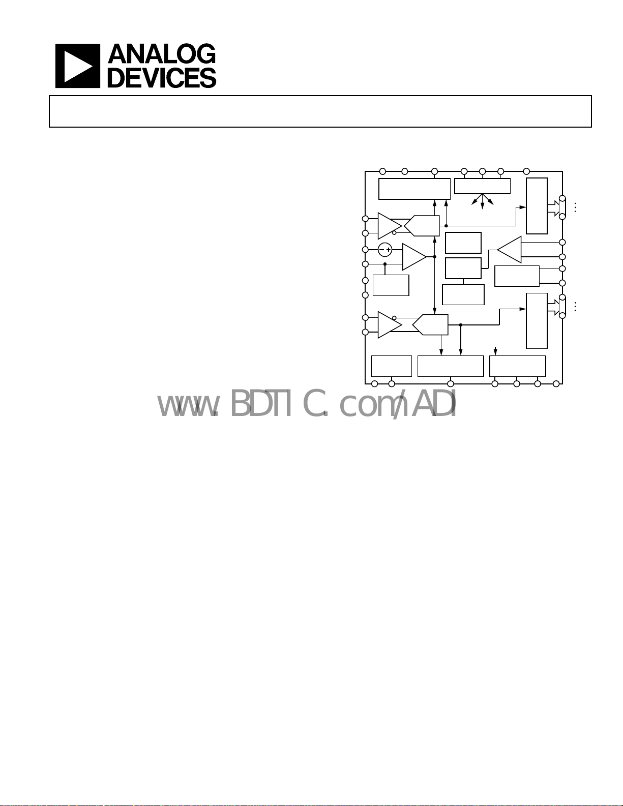
FUNCTIONAL BLOCK DIAGRAM
SCLK/
AVDD
FD BITS/THRESHOLD
VIN+A
VIN–A
VREF
SENSE
CML
RBIAS
VIN–B
VIN+B
SHA
REF
SELECT
SHA
AD9627
MULTICHI P
SYNC
AGND SYNC FD(0:3)B
NOTES
1. PIN NAMES ARE F OR THE CMO S PIN CONFIGURATION ONLY;
SEE FIGURE 7 FOR LVDS PI N NAMES.
FD(0:3)A
DVDD
DETECT
ADC
FD BITS/THRESHOLD
PRODUCT HIGHLIGHTS
1. Integrated dual, 12-bit, 80 MSPS/105 MSPS/125 MSPS/
150 MSPS ADC.
2. F
ast overrange detect and signal monitor with serial output.
3. Si
gnal monitor block with dedicated serial output mode.
4. P
roprietary differential input that maintains excellent SNR
performance for input frequencies up to 450 MHz.
5. O
peration from a single 1.8 V supply and a separate digital
output driver supply to accommodate 1.8 V to 3.3 V logic
families.
tandard serial port interface (SPI) that supports various
6. S
product features and functions, such as data formatting
(offset binary, twos complement, or gray coding), enabling
the clock DCS, power-down, test modes, and voltage
reference mode.
in compatibility with the AD9640, AD9627-11, and AD9600
7. P
for a simple migration from 12 bits to 14 bits, 11 bits, or
10 bits.
SDIO/
DCS
PROGRAMMING DATA
SIGNAL
MONITOR
DIVIDE
1 TO 8
DUTY CYCLE
STABILIZER
ADC
DETECT
Figure 1.
CSB
DFS
SPI
DCO
GENERATIO N
SIGNAL MO NITOR
DATA
SIGNAL MONITOR
INTERFACE
SMI
SMI
SCLK/
SDFS
PDWN
DRVDD
CMOS
CMOS
SMI
SDO/
OEB
D11A
D0A
OUTPUT BUFFER
CLK+
CLK–
DCOA
DCOB
D11B
D0B
OUTPUT BUF FER
DRGND
06571-001
Rev. 0
Information furnished by Analog Devices is believed to be accurate and reliable. However, no
responsibility is assumed by Anal og Devices for its use, nor for any infringements of patents or ot her
rights of third parties that may result from its use. Specifications subject to change without notice. No
license is granted by implication or otherwise under any patent or patent rights of Analog Devices.
Trademarks and registered trademarks are the property of their respective owners.
One Technology Way, P.O. Box 9106, Norwood, MA 02062-9106, U.S.A.
Tel: 781.329.4700 www.analog.com
Fax: 781.461.3113 ©2007 Analog Devices, Inc. All rights reserved.
Page 2

AD9627
www.BDTIC.com/ADI
TABLE OF CONTENTS
Features.............................................................................................. 1
Applications....................................................................................... 1
Functional Block Diagram .............................................................. 1
Product Highlights ........................................................................... 1
Revision History ............................................................................... 2
General Description ......................................................................... 3
Specifications..................................................................................... 4
ADC DC Specifications—AD9627BCPZ-80/
AD9627BCPZ-105......................................................................... 4
ADC DC Specifications—AD9627BCPZ-125/
AD9627BCPZ-150......................................................................... 5
ADC AC Specifications—AD9627BCPZ-80/
AD9627BCPZ-105......................................................................... 6
ADC AC Specifications—AD9627BCPZ-125/
AD9627BCPZ-150......................................................................... 7
Digital Specifications ................................................................... 8
Switching Specifications—AD9627BCPZ-80/
AD9627BCPZ-105....................................................................... 10
Switching Specifications—AD9627BCPZ-125/
AD9627BCPZ-150....................................................................... 11
Timing Specifications ................................................................12
Absolute Maximum Ratings.......................................................... 14
Thermal Characteristics ............................................................14
ESD Caution................................................................................ 14
Pin Configurations and Function Descriptions ......................... 15
Equivalent Circuits......................................................................... 19
Typical Performance Characteristics ........................................... 20
Theory of Operation ...................................................................... 25
ADC Architecture ......................................................................25
Analog Input Considerations.................................................... 25
Voltage Reference....................................................................... 27
Clock Input Considerations...................................................... 28
Power Dissipation and Standby Mode..................................... 30
Digital Outputs ........................................................................... 31
Timing.......................................................................................... 31
ADC Overrange and Gain Control.............................................. 32
Fast Detect Overview ................................................................. 32
ADC Fast Magnitude................................................................. 32
ADC Overrange (OR)................................................................ 33
Gain Switching............................................................................ 33
Signal Monitor................................................................................ 35
Peak Detector Mode................................................................... 35
RMS/MS Magnitude Mode......................................................... 35
Threshold Crossing Mode......................................................... 36
Additional Control Bits ............................................................. 36
DC Correction ............................................................................ 36
Signal Monitor SPORT Output ................................................ 37
Built-In Self-Test (BIST) and Output Test .................................. 38
Built-In Self-Test (BIST)............................................................ 38
Output Test Modes..................................................................... 38
Channel/Chip Synchronization.................................................... 39
Serial Port Interface (SPI).............................................................. 40
Configuration Using the SPI..................................................... 40
Hardware Interface..................................................................... 40
Configuration Without the SPI................................................ 41
SPI Accessible Features.............................................................. 41
Memory Map .................................................................................. 42
Reading the Memory Map Register Table............................... 42
Memory Map Register Table..................................................... 43
Memory Map Register Descriptions ....................................... 46
Applications Information.............................................................. 49
Design Guidelines ...................................................................... 49
Evaluation Board............................................................................ 50
Power Supplies............................................................................ 50
Input Signals................................................................................ 50
Output Signals ............................................................................ 50
Default Operation and Jumper Selection Settings................. 51
Alternative Clock Configurations............................................ 51
Alternative Analog Input Drive Configuration...................... 52
Schematics................................................................................... 53
Evaluation Board Layouts ......................................................... 63
Bill of Materials........................................................................... 71
Outline Dimensions....................................................................... 73
Ordering Guide .......................................................................... 73
REVISION HISTORY
10/07—Revision 0: Initial Version
Rev. 0 | Page 2 of 76
Page 3

AD9627
www.BDTIC.com/ADI
GENERAL DESCRIPTION
The AD9627 is a dual, 12-bit, 80 MSPS/105 MSPS/125 MSPS/
150 MSPS analog-to-digital converter (ADC). The AD9627 is
designed to support communications applications where low
cost, small size, and versatility are desired.
The dual ADC core features a multistage, differential pipelined
a
rchitecture with integrated output error correction logic. Each
ADC features wide bandwidth differential sample-and-hold
analog input amplifiers supporting a variety of user-selectable
input ranges. An integrated voltage reference eases design considerations. A duty cycle stabilizer is provided to compensate for
variations in the ADC clock duty cycle, allowing the converters
to maintain excellent performance.
The AD9627 has several functions that simplify the automatic
ga
in control (AGC) function in the system receiver. The fast detect
feature allows fast overrange detection by outputting four bits of
input level information with very short latency.
In addition, the programmable threshold detector allows monit
oring of the incoming signal power, using the four fast detect
bits of the ADC with very low latency. If the input signal level
exceeds the programmable threshold, the coarse upper threshold
cator goes high. Because this threshold indicator has very
indi
low latency, the user can quickly turn down the system gain to
avoid an overrange condition.
The second AGC-related function is the signal monitor. This block
al
lows the user to monitor the composite magnitude of the
incoming signal, which aids in setting the gain to optimize the
dynamic range of the overall system.
The ADC output data can be routed directly to the two external
12-b
it output ports. These outputs can be set from 1.8 V to 3.3 V
CMOS or 1.8 V LVDS.
Flexible power-down options allow significant power savings,
en desired.
wh
Programming for setup and control is accomplished using a 3-bit
S
PI-compatible serial interface.
The AD9627 is available in a 64-lead LFCSP and is specified over
t
he industrial temperature range of −40°C to +85°C.
Rev. 0 | Page 3 of 76
Page 4
AD9627
www.BDTIC.com/ADI
SPECIFICATIONS
ADC DC SPECIFICATIONS—AD9627BCPZ-80/AD9627BCPZ-105
AVDD = 1.8 V, DVDD = 1.8 V, DRVDD = 3.3 V, maximum sample rate, VIN = −1.0 dBFS differential input, 1.0 V internal reference, DCS
enabled, fast detect output pins disabled, and signal monitor disabled, unless otherwise noted.
Table 1.
AD9627BCPZ-80 AD9627BCPZ-105
Parameter Temperature
Min Typ Max Min Typ Max
RESOLUTION Full 12 12 Bits
ACCURACY
No Missing Codes Full Guaranteed Guaranteed
Offset Error Full ±0.2 ±0.6 ±0.3 ±0.7 % FSR
Gain Error Full +0.1 −1.8 −3.7 −0.5 −2.2 −3.7 % FSR
Differential Nonlinearity (DNL)
1
Full ±0.4 ±0.4 LSB
25°C ±0.2 ±0.2 LSB
Integral Nonlinearity (INL)
1
Full ±0.9 ±0.9 LSB
25°C ±0.4 ±0.4 LSB
MATCHING CHARACTERISTIC
Offset Error Full ±0.2 ±0.6 ±0.3 ±0.7 % FSR
Gain Error Full ±0.2 ±0.75 ±0.2 ±0.75 % FSR
TEMPERATURE DRIFT
Offset Error Full ±15 ±15 ppm/°C
Gain Error Full ±95 ±95 ppm/°C
INTERNAL VOLTAGE REFERENCE
Output Voltage Error (1 V Mode) Full ±5 ±16 ±5 ±16 mV
Load Regulation @ 1.0 mA Full 7 7 mV
INPUT REFERRED NOISE
VREF = 1.0 V 25°C 0.3 0.3 LSB rms
ANALOG INPUT
Input Span, VREF = 1.0 V Full 2 2 V p-p
Input Capacitance
2
Full 8 8 pF
VREF INPUT RESISTANCE Full 6 6 kΩ
POWER SUPPLIES
Supply Voltage
AVDD, DVDD Full 1.7 1.8 1.9 1.7 1.8 1.9 V
DRVDD (CMOS Mode) Full 1.7 3.3 3.6 1.7 3.3 3.6 V
DRVDD (LVDS Mode) Full 1.7 1.8 1.9 1.7 1.8 1.9 V
Supply Current
1, 3
I
AVDD
1, 3
I
DVDD
1
I
(3.3 V CMOS) Full 23 34 mA
DRVDD
1
I
(1.8 V CMOS) Full 11 15 mA
DRVDD
1
I
(1.8 V LVDS) Full 47 47 mA
DRVDD
Full 233 310 mA
Full 26
278
34
365
POWER CONSUMPTION
DC Input Full 452 490 600 650 mW
Sine Wave Input1 (DRVDD = 1.8 V) Full 495 657 mW
Sine Wave Input1 (DRVDD = 3.3 V) Full 550 740 mW
Standby Power
4
Full 52 68 mW
Power-Down Power Full 2.5 6 2.5 6 mW
1
Measured with a low input frequency, full-scale sine wave, with approximately 5 pF loading on each output bit.
2
Input capacitance refers to the effective capacitance between one differential input pin and AGND. See Figure 8 for the equivalent analog input structure.
3
The maximum limit applies to the combination of I
4
Standby power is measured with a dc input and with the CLK pins inactive (set to AVDD or AGND).
AVDD
and I
currents.
DVDD
Unit
mA
Rev. 0 | Page 4 of 76
Page 5
AD9627
www.BDTIC.com/ADI
ADC DC SPECIFICATIONS—AD9627BCPZ-125/AD9627BCPZ-150
AVDD = 1.8 V, DVDD = 1.8 V, DRVDD = 3.3 V, maximum sample rate, VIN = −1.0 dBFS differential input, 1.0 V internal reference, DCS
enabled, fast detect output pins disabled, and signal monitor disabled, unless otherwise noted.
Table 2.
AD9627BCPZ-125 AD9627BCPZ-150
Parameter Temperature
Min Typ Max Min Typ Max
RESOLUTION Full 12 12 Bits
ACCURACY
No Missing Codes Full Guaranteed Guaranteed
Offset Error Full ±0.3 ±0.6 ±0.2 ±0.6 % FSR
Gain Error Full −0.7 −2.7 −3.9 −0.9 −3.2 −5.2 % FSR
Differential Nonlinearity (DNL)
1
Full ±0.4 ±0.9 LSB
25°C ±0.2 ±0.2 LSB
Integral Nonlinearity (INL)
1
Full ±0.9 ±1.3 LSB
25°C ±0.4 ±0.5 LSB
MATCHING CHARACTERISTIC
Offset Error 25°C ±0.3 ±0.6 ±0.2 ±0.7 % FSR
Gain Error 25°C ±0.1 ±0.75 ±0.2 ±0.8 % FSR
TEMPERATURE DRIFT
Offset Error Full ±15 ±15 ppm/°C
Gain Error Full ±95 ±95 ppm/°C
INTERNAL VOLTAGE REFERENCE
Output Voltage Error (1 V Mode) Full ±5 ±16 ±5 ±16 mV
Load Regulation @ 1.0 mA Full 7 7 mV
INPUT REFERRED NOISE
VREF = 1.0 V 25°C 0.3 0.3 LSB rms
ANALOG INPUT
Input Span, VREF = 1.0 V Full 2 2 V p-p
Input Capacitance2 Full 8 8 pF
VREF INPUT RESISTANCE Full 6 6 kΩ
POWER SUPPLIES
Supply Voltage
AVDD, DVDD Full 1.7 1.8 1.9 1.7 1.8 1.9 V
DRVDD (CMOS Mode) Full 1.7 3.3 3.6 1.7 3.3 3.6 V
DRVDD (LVDS Mode) Full 1.7 1.8 1.9 1.7 1.8 1.9 V
Supply Current
1, 3
I
AVDD
1, 3
I
DVDD
1
I
(3.3 V CMOS) Full 36 42 mA
DRVDD
1
I
(1.8 V CMOS) Full 18 22 mA
DRVDD
1
I
(1.8 V LVDS) Full 48 49 mA
DRVDD
Full 385 419 mA
Full 42
455
50
495
POWER CONSUMPTION
DC Input Full 750 800 820 890 mW
Sine Wave Input1 (DRVDD = 1.8 V) Full 814 895 mW
Sine Wave Input1 (DRVDD = 3.3 V) Full 900 995 mW
Standby Power
4
Full 77 77 mW
Power-Down Power Full 2.5 6 2.5 6 mW
1
Measured with a low input frequency, full-scale sine wave, with approximately 5 pF loading on each output bit.
2
Input capacitance refers to the effective capacitance between one differential input pin and AGND. See Figure 8 for the equivalent analog input structure.
3
The maximum limit applies to the combination of I
4
Standby power is measured with a dc input and with the CLK pins inactive (set to AVDD or AGND).
AVDD
and I
DVDD
currents.
Unit
mA
Rev. 0 | Page 5 of 76
Page 6

AD9627
www.BDTIC.com/ADI
ADC AC SPECIFICATIONS—AD9627BCPZ-80/AD9627BCPZ-105
AVDD = 1.8 V, DVDD = 1.8 V, DRVDD = 3.3 V, maximum sample rate, VIN = −1.0 dBFS differential input, 1.0 V internal reference, DCS
enabled, fast detect output pins disabled, and signal monitor disabled, unless otherwise noted.
Table 3.
Parameter
SIGNAL-TO-NOISE RATIO (SNR)
fIN = 2.3 MHz 25°C 69.7 69.6 dB
fIN = 70 MHz 25°C 69.5 69.4 dB
Full 68.1 68.6 dB
fIN = 140 MHz 25°C 69.2 69.1 dB
fIN = 220 MHz 25°C 68.5 68.4 dB
SIGNAL-TO-NOISE AND DISTORTION (SINAD)
fIN = 2.3 MHz 25°C 69.6 69.5 dB
fIN = 70 MHz 25°C 69.4 69.3 dB
Full 67.4 68.0 dB
fIN = 140 MHz 25°C 69.0 69.0 dB
fIN = 220 MHz 25°C 68.3 68.1 dB
EFFECTIVE NUMBER OF BITS (ENOB)
fIN = 2.3 MHz 25°C 11.5 11.4 Bits
fIN = 70 MHz 25°C 11.4 11.4 Bits
fIN = 140 MHz 25°C 11.4 11.4 Bits
fIN = 220 MHz 25°C 11.3 11.2 Bits
WORST SECOND OR THIRD HARMONIC
fIN = 2.3 MHz 25°C −87 −87 dBc
fIN = 70 MHz 25°C −85 −85 dBc
Full −74 −74 dBc
fIN = 140 MHz 25°C −84 −84 dBc
fIN = 220 MHz 25°C −83 −83 dBc
SPURIOUS-FREE DYNAMIC RANGE (SFDR)
fIN = 2.3 MHz 25°C 87 87 dBc
fIN = 70 MHz 25°C 85 85 dBc
Full 74 74 dBc
fIN = 140 MHz 25°C 84 84 dBc
fIN = 220 MHz 25°C 83 83 dBc
WORST OTHER HARMONIC OR SPUR
fIN = 2.3 MHz 25°C −92 −92 dBc
fIN = 70 MHz 25°C −89 −88 dBc
Full −82 −82 dBc
fIN = 140 MHz 25°C −89 −87 dBc
fIN = 220 MHz 25°C −89 −86 dBc
TWO-TONE SFDR
fIN = 29.1 MHz, 32.1 MHz (−7 dBFS ) 25°C 85 85 dBc
fIN = 169.1 MHz, 172.1 MHz (−7 dBFS ) 25°C 82 82 dBc
CROSSTALK
ANALOG INPUT BANDWIDTH 25°C 650 650 MHz
1
See Application Note AN-835, Understanding High Speed ADC Testing and Evaluation, for a complete set of definitions.
2
Crosstalk is measured at 100 MHz with −1 dBFS on one channel and with no input on the alternate channel.
1
2
Temperature
Full −95 −95 dB
AD9627BCPZ-80 AD9627BCPZ-105
Min Typ Max Min Typ Max
Unit
Rev. 0 | Page 6 of 76
Page 7
AD9627
www.BDTIC.com/ADI
ADC AC SPECIFICATIONS—AD9627BCPZ-125/AD9627BCPZ-150
AVDD = 1.8 V, DVDD = 1.8 V, DRVDD = 3.3 V, maximum sample rate, VIN = −1.0 dBFS differential input, 1.0 V internal reference, DCS
enabled, fast detect output pins disabled, and signal monitor disabled, unless otherwise noted.
Table 4.
Parameter
SIGNAL-TO-NOISE RATIO (SNR)
fIN = 2.3 MHz 25°C 69.5 69.4 dB
fIN = 70 MHz 25°C 69.4 69.2 dB
Full 68.1 67.1 dB
fIN = 140 MHz 25°C 69.1 68.8 dB
fIN = 220 MHz 25°C 68.8 68.2 dB
SIGNAL-TO-NOISE AND DISTORTION (SINAD)
fIN = 2.3 MHz 25°C 69.4 69.3 dB
fIN = 70 MHz 25°C 69.3 69.1 dB
Full 67.9 65.9 dB
fIN = 140 MHz 25°C 69.0 68.7 dB
fIN = 220 MHz 25°C 68.3 67.8 dB
EFFECTIVE NUMBER OF BITS (ENOB)
fIN = 2.3 MHz 25°C 11.4 11.4 Bits
fIN = 70 MHz 25°C 11.4 11.4 Bits
fIN = 140 MHz 25°C 11.3 11.3 Bits
fIN = 220 MHz 25°C 11.3 11.2 Bits
WORST SECOND OR THIRD HARMONIC
fIN = 2.3 MHz 25°C −86.5 −86.5 dBc
fIN = 70 MHz 25°C −85 −84 dBc
Full −74 −73 dBc
fIN = 140 MHz 25°C −84 −83.5 dBc
fIN = 220 MHz 25°C −83 −77 dBc
SPURIOUS-FREE DYNAMIC RANGE (SFDR)
fIN = 2.3 MHz 25°C 86.5 86.5 dBc
fIN = 70 MHz 25°C 85 84 dBc
Full 74 73 dBc
fIN = 140 MHz 25°C 84 83.5 dBc
fIN = 220 MHz 25°C 83 77 dBc
WORST OTHER HARMONIC OR SPUR
fIN = 2.3 MHz 25°C −92 −92 dBc
fIN = 70 MHz 25°C −89 −88 dBc
Full −81 −80 dBc
fIN = 140 MHz 25°C −89 −88 dBc
fIN = 220 MHz 25°C −89 −88 dBc
TWO-TONE SFDR
fIN = 29.1 MHz, 32.1 MHz (−7 dBFS ) 25°C 85 85 dBc
fIN = 169.1 MHz, 172.1 MHz (−7 dBFS ) 25°C 82 82 dBc
CROSSTALK
ANALOG INPUT BANDWIDTH 25°C 650 650 MHz
1
See Application Note AN-835, Understanding High Speed ADC Testing and Evaluation, for a complete set of definitions.
2
Crosstalk is measured at 100 MHz with −1 dBFS on one channel and with no input on the alternate channel.
1
2
Temperature
Full −95 −95 dB
AD9627BCPZ-125 AD9627BCPZ-150
Min Typ Max Min Typ Max
Unit
Rev. 0 | Page 7 of 76
Page 8
AD9627
www.BDTIC.com/ADI
DIGITAL SPECIFICATIONS
AVDD = 1.8 V, DVDD = 1.8 V, DRVDD = 3.3 V, maximum sample rate, VIN = −1.0 dBFS differential input, 1.0 V internal reference, and DCS
enabled, unless otherwise noted.
Table 5.
Parameter Temperature Min Typ Max Unit
DIFFERENTIAL CLOCK INPUTS (CLK+, CLK−)
Logic Compliance CMOS/LVDS/LVPECL
Internal Common-Mode Bias Full 1.2 V
Differential Input Voltage Full 0.2 6 V p-p
Input Voltage Range Full GND − 0.3 AVDD + 1.6 V
Input Common-Mode Range Full 1.1 AVDD V
High Level Input Voltage Full 1.2 3.6 V
Low Level Input Voltage Full 0 0.8 V
High Level Input Current Full −10 +10 μA
Low Level Input Current Full −10 +10 μA
Input Capacitance Full 4 pF
Input Resistance Full 8 10 12 kΩ
SYNC INPUT
Logic Compliance CMOS
Internal Bias Full 1.2 V
Input Voltage Range Full GND − 0.3 AVDD + 1.6 V
High Level Input Voltage Full 1.2 3.6 V
Low Level Input Voltage Full 0 0.8 V
High Level Input Current Full −10 +10 μA
Low Level Input Current Full −10 +10 μA
Input Capacitance Full 4 pF
Input Resistance Full 8 10 12 kΩ
LOGIC INPUT (CSB)1
High Level Input Voltage Full 1.22 3.6 V
Low Level Input Voltage Full 0 0.6 V
High Level Input Current Full −10 +10 μA
Low Level Input Current Full 40 132 μA
Input Resistance Full 26 kΩ
Input Capacitance Full 2 pF
LOGIC INPUT (SCLK/DFS)2
High Level Input Voltage Full 1.22 3.6 V
Low Level Input Voltage Full 0 0.6 V
High Level Input Current (VIN = 3.3 V) Full −92 −135 μA
Low Level Input Current Full −10 +10 μA
Input Resistance Full 26 kΩ
Input Capacitance Full 2 pF
LOGIC INPUTS/OUTPUTS (SDIO/DCS, SMI SDFS)
High Level Input Voltage Full 1.22 3.6 V
Low Level Input Voltage Full 0 0.6 V
High Level Input Current Full −10 +10 μA
Low Level Input Current Full 38 128 μA
Input Resistance Full 26 kΩ
Input Capacitance Full 5 pF
LOGIC INPUTS/OUTPUTS (SMI SDO/OEB, SMI SCLK/PDWN)
High Level Input Voltage Full 1.22 3.6 V
Low Level Input Voltage Full 0 0.6 V
High Level Input Current (VIN = 3.3 V) Full −90 −134 μA
Low Level Input Current Full −10 +10 μA
1
2
Rev. 0 | Page 8 of 76
Page 9
AD9627
www.BDTIC.com/ADI
Parameter Temperature Min Typ Max Unit
Input Resistance Full 26 kΩ
Input Capacitance Full 5 pF
DIGITAL OUTPUTS
CMOS Mode—DRVDD = 3.3 V
High Level Output Voltage
IOH = 50 μA Full 3.29 V
IOH = 0.5 mA Full 3.25 V
Low Level Output Voltage
IOL = 1.6 mA Full 0.2 V
IOL = 50 μA Full 0.05 V
CMOS Mode—DRVDD = 1.8 V
High Level Output Voltage
IOH = 50 μA Full 1.79 V
IOH = 0.5 mA Full 1.75 V
Low Level Output Voltage
IOL = 1.6 mA Full 0.2 V
IOL = 50 μA Full 0.05 V
LVDS Mode—DRVDD = 1.8 V
Differential Output Voltage (VOD), ANSI Mode Full 250 350 450 mV
Output Offset Voltage (VOS), ANSI Mode Full 1.15 1.25 1.35 V
Differential Output Voltage (VOD), Reduced Swing Mode Full 150 200 280 mV
Output Offset Voltage (VOS), Reduced Swing Mode Full 1.15 1.25 1.35 V
1
Pull up.
2
Pull down.
Rev. 0 | Page 9 of 76
Page 10
AD9627
www.BDTIC.com/ADI
SWITCHING SPECIFICATIONS—AD9627BCPZ-80/AD9627BCPZ-105
AVDD = 1.8 V, DVDD = 1.8 V, DRVDD = 3.3 V, maximum sample rate, VIN = −1.0 dBFS differential input, 1.0 V internal reference, and
DCS enabled, unless otherwise noted.
Table 6.
AD9627BCPZ-80 AD9627BCPZ-105
Parameter Temperature
Min Typ Max Min Typ Max
CLOCK INPUT PARAMETERS
Input Clock Rate Full 625 625 MHz
Conversion Rate
DCS Enabled
DCS Disabled
CLK Period—Divide-by-1 Mode (t
1
1
Full 20 80 20 105 MSPS
Full 10 80 10 105 MSPS
) Full 12.5 9.5 ns
CLK
CLK Pulse Width High
Divide-by-1 Mode, DCS Enabled Full 3.75 6.25 8.75 2.85 4.75 6.65 ns
Divide by-1-Mode, DCS Disabled Full 5.63 6.25 6.88 4.28 4.75 5.23 ns
Divide-by-2 Mode, DCS Enabled Full 1.6 1.6 ns
Divide-by-3 Through Divide-by-8
Full 0.8 0.8 ns
Modes, DCS Enabled
DATA OUTPUT PARAMETERS (DATA, FD)
CMOS Mode—DRVDD = 3.3 V
Data Propagation Delay (tPD)
DCO Propagation Delay (t
2
) Full 3.8 5.0 6.8 3.8 5.0 6.8 ns
DCO
Full 2.2 4.5 6.4 2.2 4.5 6.4 ns
Setup Time (tS) Full 6.25 5.25 ns
Hold Time (tH) Full 5.75 4.25 ns
CMOS Mode—DRVDD = 1.8 V
Data Propagation Delay (tPD)
DCO Propagation Delay (t
2
) Full 4.0 5.6 7.3 4.0 5.6 7.3 ns
DCO
Full 2.4 5.2 6.9 2.4 5.2 6.9 ns
Setup Time (tS) Full 6.65 5.15 ns
Hold Time (tH) Full 5.85 4.35 ns
LVDS Mode—DRVDD = 1.8 V
Data Propagation Delay (tPD)
DCO Propagation Delay (t
2
) Full 5.2 7.3 9.0 5.2 7.3 9.0 ns
DCO
Full 2.0 4.8 6.3 2.0 4.8 6.3 ns
CMOS Mode Pipeline Delay (Latency) Full 12 12 Cycles
LVDS Mode Pipeline Delay (Latency)
Full 12/12.5 12/12.5 Cycles
Channel A/Channel B
Aperture Delay (tA) Full 1.0 1.0 ns
Aperture Uncertainty (Jitter, tJ) Full 0.1 0.1 ps rms
Wake-Up Time
3
Full 350 350 μs
OUT-OF-RANGE RECOVERY TIME Full 2 2 Cycles
1
Conversion rate is the clock rate after the divider.
2
Output propagation delay is measured from CLK 50% transition to DATA 50% transition, with 5 pF load.
3
Wake-up time is dependent on the value of the decoupling capacitors.
Unit
Rev. 0 | Page 10 of 76
Page 11
AD9627
www.BDTIC.com/ADI
SWITCHING SPECIFICATIONS—AD9627BCPZ-125/AD9627BCPZ-150
AVDD = 1.8 V, DVDD = 1.8 V, DRVDD = 3.3 V, maximum sample rate, VIN = −1.0 dBFS differential input, 1.0 V internal reference, and
DCS enabled, unless otherwise noted.
Table 7.
AD9627BCPZ-125 AD9627BCPZ-150
Parameter Temperature
Min Typ Max Min Typ Max
CLOCK INPUT PARAMETERS
Input Clock Rate Full 625 625 MHz
Conversion Rate
DCS Enabled
DCS Disabled
CLK Period—Divide-by-1 Mode (t
1
1
CLK
Full 20 125 20 150 MSPS
Full 10 125 10 150 MSPS
) Full 8 6.66 ns
CLK Pulse Width High
Divide-by-1 Mode, DCS Enabled Full 2.4 4 5.6 2.0 3.33 4.66 ns
Divide-by-1 Mode, DCS Disabled Full 3.6 4 4.4 3.0 3.33 3.66 ns
Divide-by-2 Mode, DCS Enabled Full 1.6 1.6 ns
Divide-by-3 Through Divide-by-8
Full 0.8 0.8 ns
Modes, DCS Enabled
DATA OUTPUT PARAMETERS (DATA, FD)
CMOS Mode—DRVDD = 3.3 V
Data Propagation Delay (tPD)
DCO Propagation Delay (t
2
) Full 3.8 5.0 6.8 3.8 5.0 6.8 ns
DCO
Full 2.2 4.5 6.4 2.2 4.5 6.4 ns
Setup Time (tS) Full 4.5 3.83 ns
Hold Time (tH) Full 3.5 2.83 ns
CMOS Mode—DRVDD = 1.8 V
Data Propagation Delay (tPD)
DCO Propagation Delay (t
2
) Full 4.0 5.6 7.3 4.0 5.6 7.3 ns
DCO
Full 2.4 5.2 6.9 2.4 5.2 6.9 ns
Setup Time (tS) Full 4.4 3.73 ns
Hold Time (tH) Full 3.6 2.93 ns
LVDS Mode—DRVDD = 1.8 V
Data Propagation Delay (tPD)
DCO Propagation Delay (t
2
) Full 5.2 7.3 9.0 5.2 7.3 9.0 ns
DCO
Full 2.0 4.8 6.3 2.0 4.8 6.3 ns
CMOS Mode Pipeline Delay (Latency) Full 12 12 Cycles
LVDS Mode Pipeline Delay (Latency)
Full 12/12.5 12/12.5 Cycles
Channel A/Channel B
Aperture Delay (tA) Full 1.0 1.0 ns
Aperture Uncertainty (Jitter, tJ) Full 0.1 0.1 ps rms
Wake-Up Time
3
Full 350 350 μs
OUT-OF-RANGE RECOVERY TIME Full 3 3 Cycles
1
Conversion rate is the clock rate after the divider.
2
Output propagation delay is measured from CLK 50% transition to DATA 50% transition, with 5 pF load.
3
Wake-up time is dependent on the value of the decoupling capacitors.
Unit
Rev. 0 | Page 11 of 76
Page 12
AD9627
C
A
www.BDTIC.com/ADI
TIMING SPECIFICATIONS
Table 8.
Parameter Conditions Min Typ Max Unit
SYNC TIMING REQUIREMENTS
t
SSYNC
t
HSYNC
SPI TIMING REQUIREMENTS
t
DS
t
DH
t
CLK
t
S
t
H
t
HIGH
t
LOW
t
EN_SDIO
t
DIS_SDIO
SPORT TIMING REQUIREMENTS
t
CSSCLK
t
SSCLKSDO
t
SSCLKSDFS
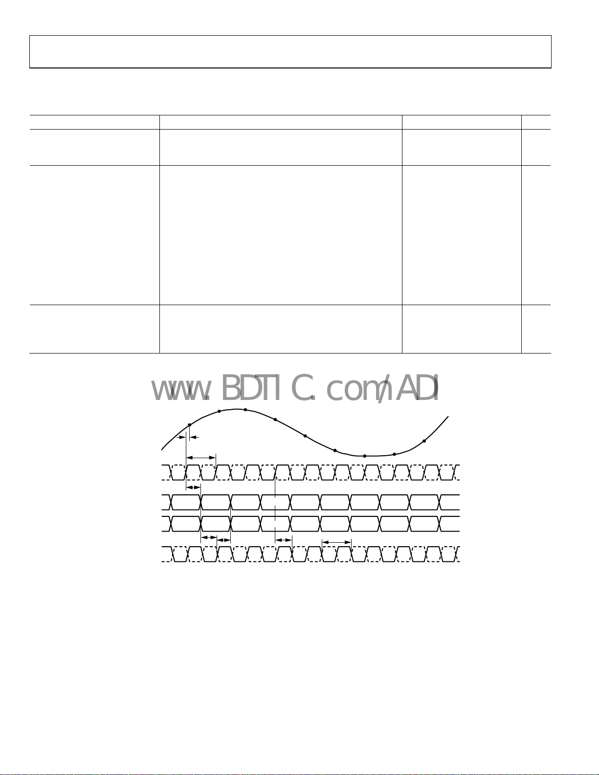
Timing Diagrams
H A/CH B DAT
SYNC to rising edge of CLK setup time 0.24 ns
SYNC to rising edge of CLK hold time 0.40 ns
Setup time between the data and the rising edge of SCLK 2 ns
Hold time between the data and the rising edge of SCLK 2 ns
Period of the SCLK 40 ns
Setup time between CSB and SCLK 2 ns
Hold time between CSB and SCLK 2 ns
SCLK pulse width high 10 ns
SCLK pulse width low 10 ns
Time required for the SDIO pin to switch from an input to an
10 ns
output relative to the SCLK falling edge
Time required for the SDIO pin to switch from an output to an
10 ns
input relative to the SCLK rising edge
Delay from rising edge of CLK+ to rising edge of SMI SCLK 3.2 4.5 6.2 ns
Delay from rising edge of SMI SCLK to SMI SDO −0.4 0 0.4 ns
Delay from rising edge of SMI SCLK to SMI SDFS −0.4 0 0.4 ns
N+2
CLK+
CLK–
N+ 1
N
t
A
t
CLK
t
PD
N – 12 N – 11 N – 9 N – 8 N – 7 N – 6 N – 5 N – 4
N – 13
N+ 3
N – 10
N+ 4
N+ 5
N+ 6
N+ 8
N+ 7
CH A/CH B FAST
DETECT
t
S
DCOA/DCOB
Figure 2. CMOS Output Mode Data an
N – 1 N + 2 N + 3 N + 4 N + 5 N + 6N – 3 N – 2
t
H
N
d Fast Detect Output Timing (Fast Detect Mode Select Bits = 000)
Rev. 0 | Page 12 of 76
t
N + 1
DCO
t
CLK
06571-002
Page 13
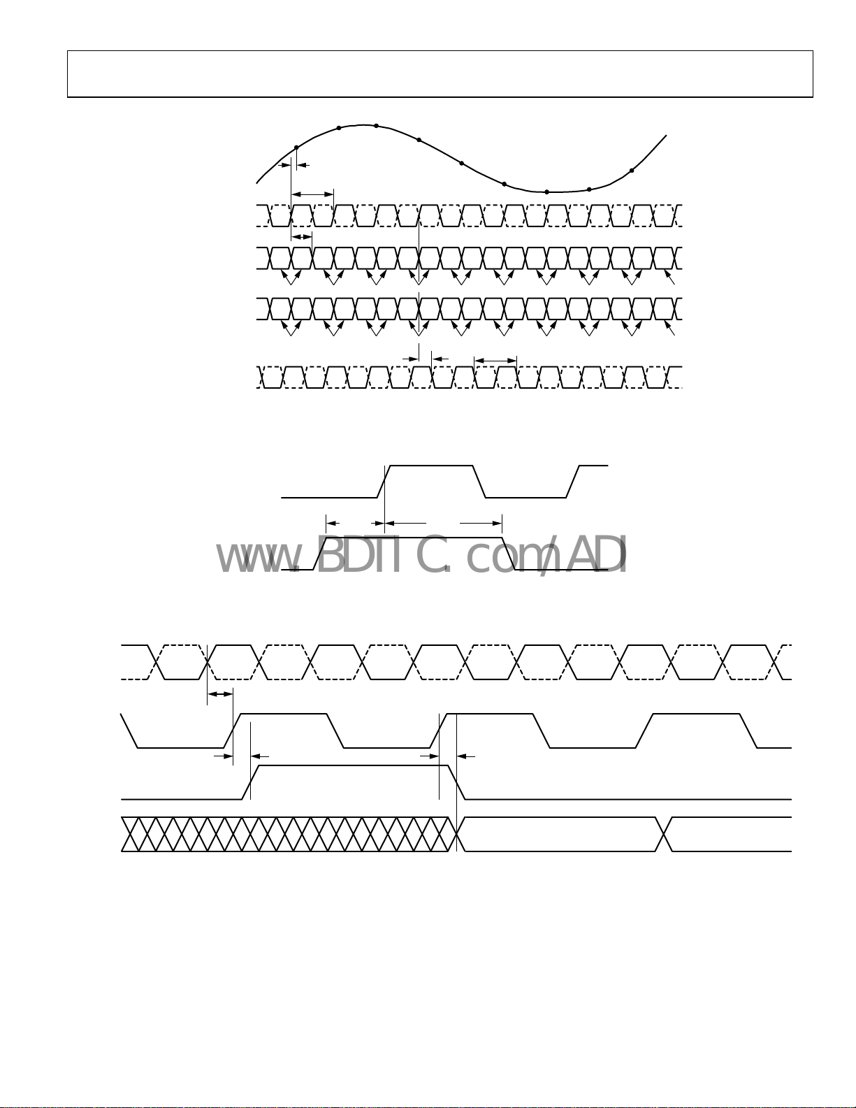
AD9627
C
A
www.BDTIC.com/ADI
N
t
A
CLK+
CLK–
H A/CH B DAT
CH A/CH B F AST
DETECT
DCO+
DCO–
t
PD
ABABABABABABABABA AB
N – 13
N – 12 N – 11 N – 9 N – 8 N – 7 N – 6 N – 5 N – 4
ABABABABABABABABA AB
N – 6 N – 5 N – 3 N – 2 N – 1 N N + 1 N + 2N – 7
Figure 3. LVDS Mode Data and Fast Detect Output Timing (Fast Detect M
N+ 1
t
CLK
N+2
N+ 3
N – 10
N – 4
t
DCO
N+ 4
N+ 5
t
N+ 6
CLK
N+ 8
N+ 7
ode Select Bits = 001 Through Fast Detect Mode Select Bits = 100)
06571-003
CLK+
CLK+
CLK–
SMI SCLK
SMI SDFS
t
CSSCLK
t
SSYNC
SYNC
Figure 4. SYNC Input Timing Requirements
t
SSCLKSDFS
Figure 5. Signal Monitor SPORT Outpu
t
HSYNC
t
SSCLKSDO
DATA DATASMI SDO
t Timing (Divide-by-2 Mode)
06571-004
06571-005
Rev. 0 | Page 13 of 76
Page 14
AD9627
www.BDTIC.com/ADI
ABSOLUTE MAXIMUM RATINGS
Table 9.
Parameter Rating
ELECTRICAL
AVDD, DVDD to AGND −0.3 V to +2.0 V
DRVDD to DRGND −0.3 V to +3.9 V
AGND to DRGND −0.3 V to +0.3 V
AVDD to DRVDD −3.9 V to +2.0 V
VIN+A/VIN+B, VIN−A/VIN−B to AGND −0.3 V to AVDD + 0.2 V
CLK+, CLK− to AGND −0.3 V to +3.9 V
SYNC to AGND −0.3 V to +3.9 V
VREF to AGND −0.3 V to AVDD + 0.2 V
SENSE to AGND −0.3 V to AVDD + 0.2 V
CML to AGND −0.3 V to AVDD + 0.2 V
RBIAS to AGND −0.3 V to AVDD + 0.2 V
CSB to AGND −0.3 V to +3.9 V
SCLK/DFS to DRGND −0.3 V to +3.9 V
SDIO/DCS to DRGND −0.3 V to DRVDD + 0.3 V
SMI SDO/OEB −0.3 V to DRVDD + 0.3 V
SMI SCLK/PDWN −0.3 V to DRVDD + 0.3 V
SMI SDFS −0.3 V to DRVDD + 0.3 V
D0A/D0B through D11A/D11B to
DRGND
FD0A/FD0B through FD3A/FD3B to
DRGND
DCOA/DCOB to DRGND
−0.3 V to DRVDD + 0.3 V
−0.3 V to DRVDD + 0.3 V
−0.3 V to DRVDD + 0.3 V
ENVIRONMENTAL
Operating Temperature Range
−40°C to +85°C
(Ambient)
Maximum Junction Temperature
150°C
Under Bias
Storage Temperature Range
−65°C to +150°C
(Ambient)
Stresses above those listed under Absolute Maximum Ratings
y cause permanent damage to the device. This is a stress
ma
rating only; functional operation of the device at these or any
other conditions above those indicated in the operational
section of this specification is not implied. Exposure to absolute
maximum rating conditions for extended periods may affect
device reliability.
THERMAL CHARACTERISTICS
The exposed paddle must be soldered to the ground plane for
the LFCSP package. Soldering the exposed paddle to the customer
board increases the reliability of the solder joints and maximizes
the thermal capability of the package.
Table 10. Thermal Resistance
Airflow
Package
Typ e
64-Lead LFCSP
9 mm × 9 mm
(CP-64-3)
1
Per JEDEC 51-7, plus JEDEC 25-5 2S2P test board.
2
Per JEDEC JESD51-2 (still air) or JEDEC JESD51-6 (moving air).
3
Per MIL-Std 883, Method 1012.1.
4
Per JEDEC JESD51-8 (still air).
Ve
lo city
(m/s) θ
1, 2
JA
1, 3
θ
JC
1, 4
θ
Unit
JB
0 18.8 0.6 6.0 °C/W
1.0 16.5 °C/W
2.0 15.8 °C/W
Typical θJA is specified for a 4-layer PCB with a solid ground
plane. As shown, airflow improves heat dissipation, which
reduces θ
. In addition, metal in direct contact with the package
JA
leads from metal traces, through holes, ground, and power
planes, reduces the θ
.
JA
ESD CAUTION
Rev. 0 | Page 14 of 76
Page 15
AD9627
www.BDTIC.com/ADI
PIN CONFIGURATIONS AND FUNCTION DESCRIPTIONS
DRGND
D3B
D2B
D1B
D0B (LSB)
DNC
DNC
DVDD
FD3B
FD2B
FD1B
FD0B
SYNC
CSB
CLK–
CLK+
49
48
SCLK/DFS
47
SDIO/DCS
46
AVDD
45
AVDD
44
VIN+B
43
VIN–B
42
RBIAS
41
CML
40
SENSE
39
VREF
38
VIN–A
37
VIN+A
36
AVDD
35
SMI SDFS
34
SMI SCLK/PDWN
33
SMI SDO/OEB
DRVDD
D4B
D5B
D6B
D7B
D8B
D9B
D10B
D11B (MSB)
DCOB
DCOA
DNC
DNC
D0A (LSB)
D1A
D2A
646362616059585756555453525150
PIN 1
1
2
3
4
5
6
7
8
9
10
11
12
13
14
15
16
INDICATO R
EXPOSED PADDLE, PIN 0
(BOTTOM OF PACKAGE)
AD9627
PARALLEL CMOS
TOP VIEW
(Not to Scale)
DNC = DO NOT CONNECT
171819202122232425262728293031
D3A
D4A
D5A
D6A
D7A
D8A
D9A
D10A
FD0A
DRGND
DRVDD
DVDD
FD1A
D11A (MSB)
32
FD2A
FD3A
06571-006
Figure 6. LFCSP Parallel CMOS Pin Configuration (Top View)
Table 11. Pin Function Descriptions (Parallel CMOS Mode)
Pin No. Mnemonic Type Description
ADC Power Supplies
20, 64 DRGND Ground Digital Output Ground.
1, 21 DRVDD Supply Digital Output Driver Supply (1.8 V to 3.3 V).
24, 57 DVDD Supply Digital Power Supply (1.8 V Nominal).
36, 45, 46 AVDD Supply Analog Power Supply (1.8 V Nominal).
0 AGND Ground Analog Ground. Pin 0 is the exposed thermal pad on the bottom of the package.
12, 13, 58, 59 DNC Do Not Connect.
ADC Analog
37 VIN+A Input Differential Analog Input Pin (+) for Channel A.
38 VIN−A Input Differential Analog Input Pin (−) for Channel A.
44 VIN+B Input Differential Analog Input Pin (+) for Channel B.
43 VIN−B Input Differential Analog Input Pin (−) for Channel B.
39 VREF Input/Output Voltage Reference Input/Output.
40 SENSE Input Voltage Reference Mode Select. See Tab le 14 for details.
42 RBIAS Input/Output External Reference Bias Resistor.
41 CML Output Common-Mode Level Bias Output for Analog Inputs.
49 CLK+ Input ADC Clock Input—True.
50 CLK− Input ADC Clock Input—Complement.
ADC Fast Detect Outputs
29 FD0A Output Channel A Fast Detect Indicator. See Tab le 17 for details.
30 FD1A Output Channel A Fast Detect Indicator. See Tab le 17 for details.
31 FD2A Output Channel A Fast Detect Indicator. See Tab le 17 for details.
32 FD3A Output Channel A Fast Detect Indicator. See Tab le 17 for details.
53 FD0B Output Channel B Fast Detect Indicator. See Table 17 for details.
54 FD1B Output Channel B Fast Detect Indicator. See Table 17 for details.
55 FD2B Output Channel B Fast Detect Indicator. See Table 17 for details.
56 FD3B Output Channel B Fast Detect Indicator. See Table 17 for details.
Digital Input
52 SYNC Input Digital Synchronization Pin. Slave mode only.
Rev. 0 | Page 15 of 76
Page 16
AD9627
www.BDTIC.com/ADI
Pin No. Mnemonic Type Description
Digital Outputs
14 D0A (LSB) Output Channel A CMOS Output Data.
15 D1A Output Channel A CMOS Output Data.
16 D2A Output Channel A CMOS Output Data.
17 D3A Output Channel A CMOS Output Data.
18 D4A Output Channel A CMOS Output Data.
19 D5A Output Channel A CMOS Output Data.
22 D6A Output Channel A CMOS Output Data.
23 D7A Output Channel A CMOS Output Data.
25 D8A Output Channel A CMOS Output Data.
26 D9A Output Channel A CMOS Output Data.
27 D10A Output Channel A CMOS Output Data.
28 D11A (MSB) Output Channel A CMOS Output Data.
60 D0B (LSB) Output Channel B CMOS Output Data.
61 D1B Output Channel B CMOS Output Data.
62 D2B Output Channel B CMOS Output Data.
63 D3B Output Channel B CMOS Output Data.
2 D4B Output Channel B CMOS Output Data.
3 D5B Output Channel B CMOS Output Data.
4 D6B Output Channel B CMOS Output Data.
5 D7B Output Channel B CMOS Output Data.
6 D8B Output Channel B CMOS Output Data.
7 D9B Output Channel B CMOS Output Data.
8 D10B Output Channel B CMOS Output Data.
9 D11B (MSB) Output Channel B CMOS Output Data.
11 DCOA Output Channel A Data Clock Output.
10 DCOB Output Channel B Data Clock Output.
SPI Control
48 SCLK/DFS Input SPI Serial Clock/Data Format Select Pin in External Pin Mode.
47 SDIO/DCS Input/Output SPI Serial Data I/O/Duty Cycle Stabilizer Pin in External Pin Mode.
51 CSB Input SPI Chip Select (Active Low).
Signal Monitor Port
33 SMI SDO/OEB Input/Output Signal Monitor Serial Data Output/Output Enable Input (Active Low) in External Pin Mode.
35 SMI SDFS Output Signal Monitor Serial Data Frame Sync.
34 SMI SCLK/PDWN Input/Output Signal Monitor Serial Clock Output/Power-Down Input in External Pin Mode.
Rev. 0 | Page 16 of 76
Page 17
AD9627
www.BDTIC.com/ADI
DRGND
DNC
DNC
FD3+
FD3–
FD2+
FD2–
DVDD
FD1+
FD1–
FD0+
FD0–
SYNC
CSB
CLK–
CLK+
49
48
SCLK/DFS
47
SDIO/DCS
46
AVDD
45
AVDD
44
VIN+B
43
VIN–B
42
RBIAS
41
CML
40
SENSE
39
VREF
38
VIN–A
37
VIN+A
36
AVDD
35
SMI SDFS
34
SMI SCLK/PDWN
33
SMI SDO/OEB
DRVDD
DNC
DNC
D0– (LSB)
D0+ (LSB)
D1–
D1+
D2–
D2+
DCO–
DCO+
D3–
D3+
D4–
D4+
D5–
646362616059585756555453525150
PIN 1
1
2
3
4
5
6
7
8
9
10
11
12
13
14
15
16
INDICATO R
EXPOSED PADDLE, PIN 0
(BOTTOM OF PACKAGE)
AD9627
PARALLEL LVDS
TOP VIEW
(Not to Scale)
DNC = DO NOT CONNECT
171819202122232425262728293031
D6–
D7–
D8–
D5+
D6+
DRGND
DRVDD
D7+
DVDD
D8+
D9–
D9+
D10–
D10+
32
D11– (MSB)
D11+ (MSB)
06571-007
Figure 7. LFCSP Interleaved Parallel LVDS Pin Configuration (Top View)
Table 12. Pin Function Descriptions (Interleaved Parallel LVDS Mode)
Pin No. Mnemonic Type Description
ADC Power Supplies
20, 64 DRGND Ground Digital Output Ground.
1, 21 DRVDD Supply Digital Output Driver Supply (1.8 V to 3.3 V).
24, 57 DVDD Supply Digital Power Supply (1.8 V Nominal).
36, 45, 46 AVDD Supply Analog Power Supply (1.8 V Nominal).
0 AGND Ground Analog Ground. Pin 0 is the exposed thermal pad on the bottom of the package.
2, 3, 62,
DNC Do Not Connect.
63
ADC Analog
37 VIN+A Input Differential Analog Input Pin (+) for Channel A.
38 VIN−A Input Differential Analog Input Pin (−) for Channel A.
44 VIN+B Input Differential Analog Input Pin (+) for Channel B.
43 VIN−B Input Differential Analog Input Pin (−) for Channel B.
39 VREF Input/Output Voltage Reference Input/Output.
40 SENSE Input Voltage Reference Mode Select. See Table 14 for details.
42 RBIAS Input/Output External Reference Bias Resistor.
41 CML Output Common-Mode Level Bias Output for Analog Inputs.
49 CLK+ Input ADC Clock Input—True.
50 CLK− Input ADC Clock Input—Complement.
ADC Fast Detect Outputs
54 FD0+ Output Channel A/Channel B LVDS Fast Detect Indicator 0—True. See Table 17 for details.
53 FD0− Output Channel A/Channel B LVDS Fast Detect Indicator 0—Complement. See Table 17 for details.
56 FD1+ Output Channel A/Channel B LVDS Fast Detect Indicator 1—True. See Table 17 for details.
55 FD1− Output Channel A/Channel B LVDS Fast Detect Indicator 1—Complement. See Table 17 for details.
59 FD2+ Output Channel A/Channel B LVDS Fast Detect Indicator 2—True. See Table 17 for details.
58 FD2− Output Channel A/Channel B LVDS Fast Detect Indicator 2—Complement. See Table 17 for details.
61 FD3+ Output Channel A/Channel B LVDS Fast Detect Indicator 3—True. See Table 17 for details.
60 FD3− Output Channel A/Channel B LVDS Fast Detect Indicator 3—Complement. See Table 17 for details.
Digital Input
52 SYNC Input Digital Synchronization Pin. Slave mode only.
Rev. 0 | Page 17 of 76
Page 18
AD9627
www.BDTIC.com/ADI
Pin No. Mnemonic Type Description
Digital Outputs
5 D0+ (LSB) Output Channel A/Channel B LVDS Output Data 0—True.
4 D0− (LSB) Output Channel A/Channel B LVDS Output Data 0—Complement.
7 D1+ Output Channel A/Channel B LVDS Output Data 1—True.
6 D1− Output Channel A/Channel B LVDS Output Data 1—Complement.
9 D2+ Output Channel A/Channel B LVDS Output Data 2—True.
8 D2− Output Channel A/Channel B LVDS Output Data 2—Complement.
13 D3+ Output Channel A/Channel B LVDS Output Data 3—True.
12 D3− Output Channel A/Channel B LVDS Output Data 3—Complement.
15 D4+ Output Channel A/Channel B LVDS Output Data 4 —True.
14 D4− Output Channel A/Channel B LVDS Output Data 4—Complement.
17 D5+ Output Channel A/Channel B LVDS Output Data 5—True.
16 D5− Output Channel A/Channel B LVDS Output Data 5—Complement.
19 D6+ Output Channel A/Channel B LVDS Output Data 6—True.
18 D6− Output Channel A/Channel B LVDS Output Data 6—Complement.
23 D7+ Output Channel A/Channel B LVDS Output Data 7—True.
22 D7− Output Channel A/Channel B LVDS Output Data 7—Complement.
26 D8+ Output Channel A/Channel B LVDS Output Data 8—True.
25 D8− Output Channel A/Channel B LVDS Output Data 8—Complement.
28 D9+ Output Channel A/Channel B LVDS Output Data 9—True.
27 D9− Output Channel A/Channel B LVDS Output Data 9—Complement.
30 D10+ Output Channel A/Channel B LVDS Output Data 10—True.
29 D10− Output Channel A/Channel B LVDS Output Data 10—Complement.
32 D11+ (MSB) Output Channel A/Channel B LVDS Output Data 11—True.
31 D11− (MSB) Output Channel A/Channel B LVDS Output Data 11—Complement.
11 DCO+ Output Channel A/Channel B LVDS Data Clock Output—True.
10 DCO− Output Channel A/Channel B LVDS Data Clock Output—Complement.
SPI Control
48 SCLK/DFS Input SPI Serial Clock/Data Format Select Pin in External Pin Mode.
47 SDIO/DCS Input/Output SPI Serial Data I/O/Duty Cycle Stabilizer Pin in External Pin Mode.
51 CSB Input SPI Chip Select (Active Low).
Signal Monitor Port
33 SMI SDO/OEB Input/Output Signal Monitor Serial Data Output/Output Enable Input (Active Low) in External Pin Mode.
35 SMI SDFS Output Signal Monitor Serial Data Frame Sync.
34 SMI SCLK/PDWN Input/Output Signal Monitor Serial Clock Output/Power-Down Input in External Pin Mode.
Rev. 0 | Page 18 of 76
Page 19
AD9627
V
C
S
V
www.BDTIC.com/ADI
EQUIVALENT CIRCUITS
LK+
IN
06571-008
Figure 8. Equivalent Analog Input Circuit
AVDD
1.2V
10kΩ 10kΩ
Figure 9. Equivalent Clock Input Circuit
DRVDD
CLK–
SCLK/DFS
26kΩ
1kΩ
06571-012
Figure 12. Equivalent SCLK/DFS Input Circuit
SENSE
06571-009
1kΩ
06571-013
Figure 13. Equivalent SENSE Circuit
AVDD
26kΩ
CSB
1kΩ
DRGND
6571-010
Figure 10. Digital Output
DRVDD
DRVDD
26kΩ
DIO/DCS
1kΩ
06571-011
Figure 11. Equivalent SDIO/DCS or SMI SDFS Circuit
Rev. 0 | Page 19 of 76
Figure 14. Equivalent CSB Input Circuit
AVDD
REF
6kΩ
06571-015
Figure 15. Equivalent VREF Circuit
06571-014
Page 20
AD9627
www.BDTIC.com/ADI
TYPICAL PERFORMANCE CHARACTERISTICS
AVDD = 1.8 V, DVDD = 1.8 V, DRVDD = 3.3 V, sample rate = 150 MSPS, DCS enabled, 1.0 V internal reference, 2 V p-p differential input,
VIN = −1.0 dBFS, and 64k sample, T
0
–20
–40
= 25°C, unless otherwise noted.
A
150MSPS
2.3MHz @ –1dBF S
SNR = 69.4dBc (70.4dBFS)
ENOB = 11.4 BI TS
SFDR = 86.5dBc
–20
–40
0
150MSPS
140MHz @ –1dBFS
SNR = 68.8dBc (69.8dBFS)
ENOB = 11.3 BITS
SFDR = 83.5d Bc
–60
–80
AMPLITUDE ( dBFS)
–100
–120
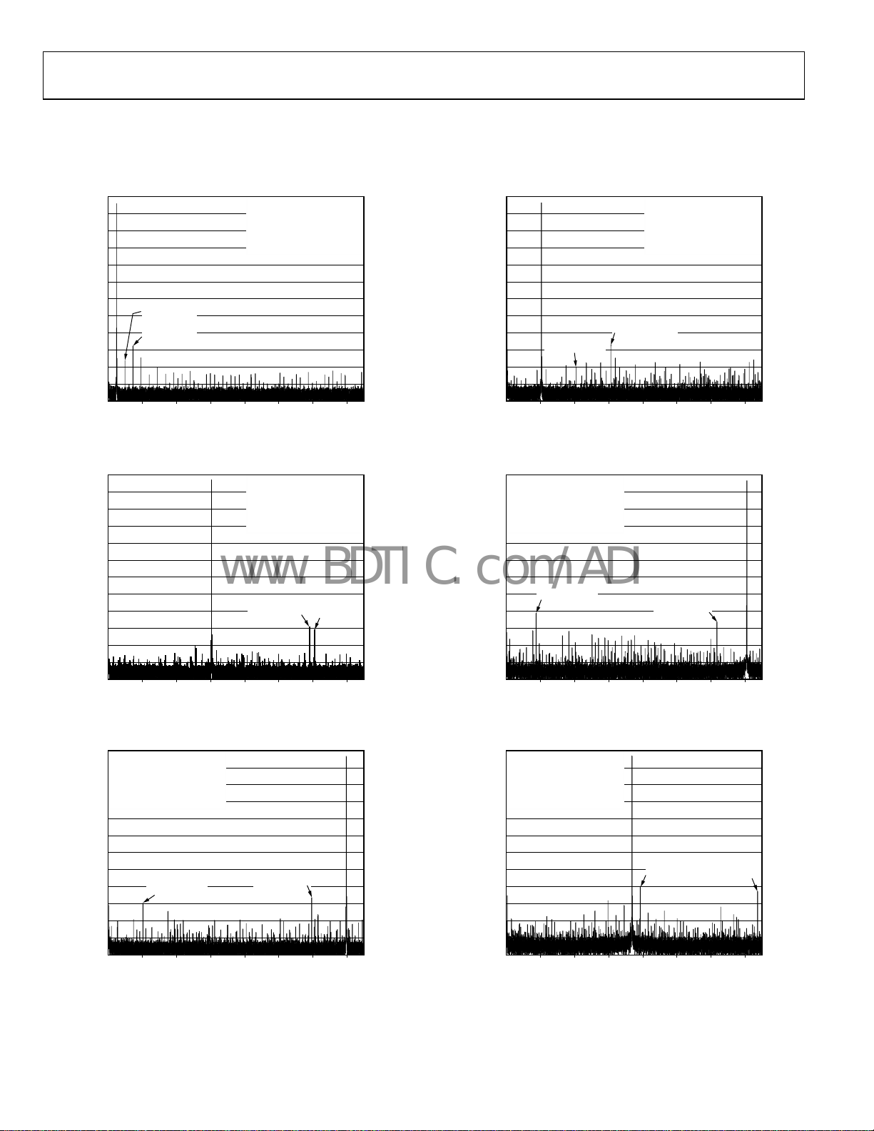
Figure 16. AD9627-150 Single-Tone FFT with f
0
–20
–40
–60
–80
AMPLITUDE ( dBFS)
–100
–120
Figure 17. AD9627-150 Single-Tone FFT with f
SECOND
HARMONIC
THIRD
HARMONIC
07
07
FREQUENCY (MHz)
150MSPS
30.3MHz @ –1dBF S
SNR = 69.3dBc (70.3dBFS)
ENOB = 11.4 BITS
SFDR = 84.0d Bc
HARMONIC
FREQUENCY (MHz)
THIRD
605040302010
= 2.3 MHz
IN
SECOND
HARMONIC
605040302010
= 30.3 MHz
IN
0
06571-016
0
06571-017
–60
–80
AMPLITUDE ( dBFS)
–100
–120
070605040302010
Figure 19. AD9627-150 Single-Tone FFT with f
0
–20
–40
–60
–80
AMPLITUDE ( dBFS)
–100
–120
070605040302010
Figure 20. AD9627-150 Single-Tone FFT with f
SECOND
HARMONIC
FREQUENCY (MHz)
150MSPS
220MHz @ –1dBFS
SNR = 68.2dBc (69. 2dBFS)
ENOB = 11.2 BITS
SFDR = 77.0dBc
SECOND
HARMONIC
FREQUENCY (MHz)
THIRD
HARMONIC
THIRD
HARMONIC
= 140 MHz
IN
= 220 MHz
IN
06571-019
06571-020
0
150MSPS
70MHz @ –1dBFS
SNR = 69.2dBc (70. 2dBFS)
–20
ENOB = 11.4 BITS
SFDR = 84.0dBc
–40
–60
–80
AMPLITUDE ( dBFS)
–100
–120
07
SECOND
HARMONIC
FREQUENCY (MHz)
Figure 18. AD9627-150 Single-Tone FFT with f
THIRD
HARMONIC
605040302010
= 70 MHz
IN
0
06571-018
Rev. 0 | Page 20 of 76
0
150MSPS
337MHz @ –1dBFS
SNR = 67.6dBc (68. 6dBFS)
–20
ENOB = 11.1 BITS
SFDR = 74.0dBc
–40
–60
–80
AMPLITUDE ( dBFS)
–100
–120
070605040302010
FREQUENCY (MHz)
THIRD
HARMONIC
Figure 21. AD9627-150 Single-Tone FFT with f
SECOND
HARMONIC
= 337 MHz
IN
06571-021
Page 21
AD9627
www.BDTIC.com/ADI
0
125MSPS
70MHz @ –1dBFS
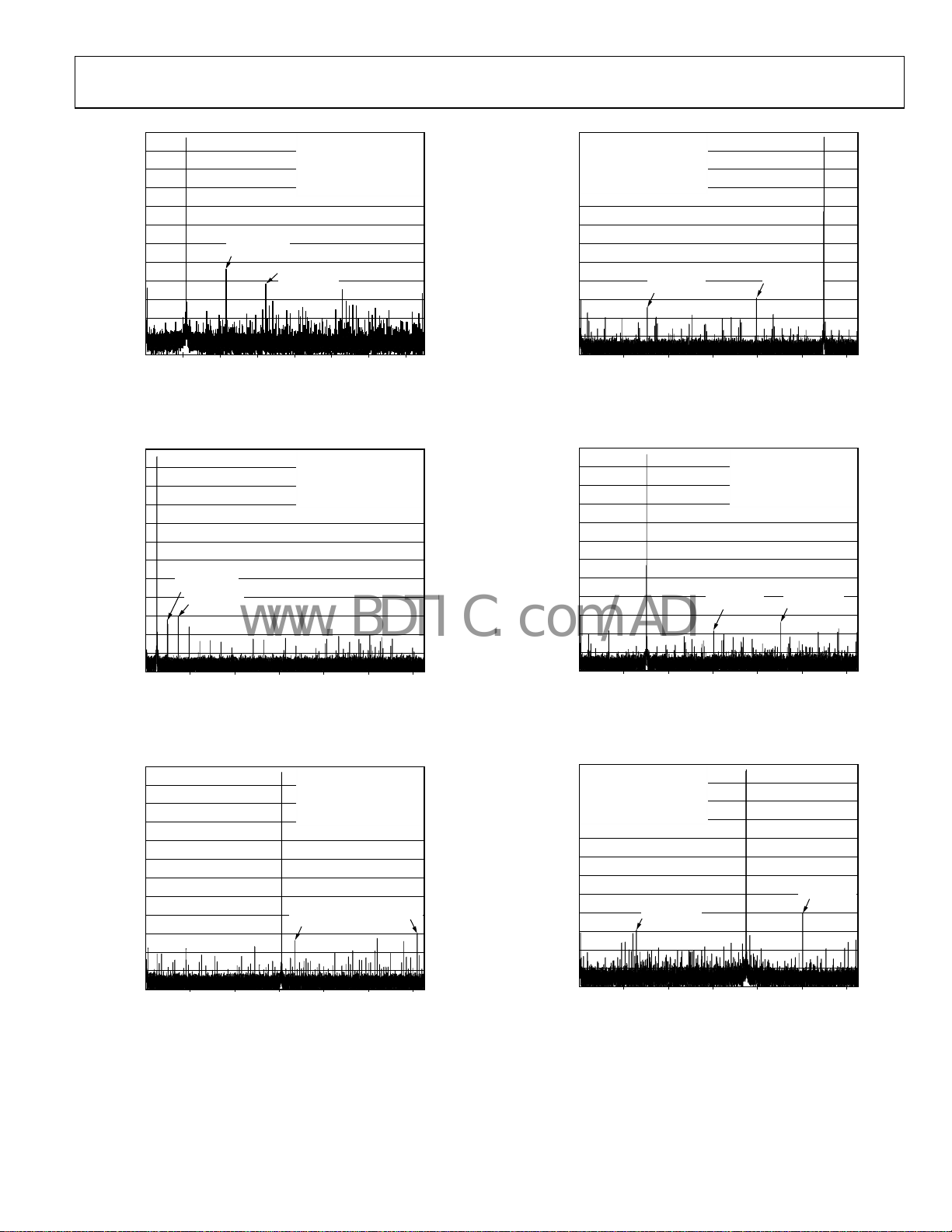
SNR = 69.4dBc (70. 4dBFS)
–20
ENOB = 11.4 BITS
SFDR = 85dBc
–40
–20
–40
0
150MSPS
440MHz @ –1dBFS
SNR = 65.7dBc (66.7dBFS)
ENOB = 10.4 BITS
SFDR = 70.0d Bc
–60
–80
AMPLITUDE ( dBFS)
100
–
–120
07
Figure 22. AD9627-150 Single-Tone FFT with f
0
–20
–40
–60
–80
AMPLITUDE ( dBFS)
–100
–120
SECOND
HARMONIC
06
Figure 23. AD9627-125 Single-Tone FFT with f
SECOND
HARMONIC
THIRD
HARMONIC
THIRD
HARMONIC
FREQUENCY (MHz)
125MSPS
2.3MHz @ –1dBF S
SNR = 69.5dBc (70.5dBFS)
ENOB = 11.4 BITS
SFDR = 86.5d Bc
FREQUENCY (MHz)
605040302010
= 440 MHz
IN
5040302010
= 2.3 MHz
IN
0
06571-022
0
06571-023
–60
–80
AMPLITUDE ( dBFS)
–100
–120
0605040302010
Figure 25. AD9627-125 Single-Tone FFT with f
0
–20
–40
–60
–80
AMPLITUDE ( dBFS)
–100
–120
0605040302010
Figure 26. AD9627-125 Single-Tone FFT with f
SECOND
HARMONIC
FREQUENCY (MHz)
FREQUENCY (MHz)
THIRD
HARMONIC
125MSPS
140MHz @ –1dBFS
SNR = 69.1dBc (70.1dBFS)
ENOB = 11.3 BITS
SFDR = 84dBc
SECOND
HARMONIC
= 70 MHz
IN
THIRD
HARMONIC
= 140 MHz
IN
06571-025
06571-026
0
–20
–40
–60
–80
AMPLITUDE ( dBFS)
–100
–120
06
FREQUENCY (MHz)
Figure 24. AD9627-125 Single-Tone FFT with f
125MSPS
30.3MHz @ –1dBF S
SNR = 69.4dBc (70.4dBFS)
ENOB = 11.4 BITS
SFDR = 85dBc
THIRD
HARMONIC
SECOND
HARMONIC
5040302010
= 30.3 MHz
IN
0
06571-024
0
125MSPS
337MHz @ –1dBFS
SNR = 67.6dBc (68. 6dBFS)
–20
ENOB = 11.1 BITS
SFDR = 74dBc
–40
–60
–80
AMPLITUDE ( dBFS)
–100
–120
0605040302010
Figure 27. AD9627-125 Single-Tone FFT with f
Rev. 0 | Page 21 of 76
THIRD
HARMONIC
FREQUENCY (MHz)
SECOND
HARMONIC
= 337 MHz
IN
06571-027
Page 22
AD9627
–
www.BDTIC.com/ADI
120
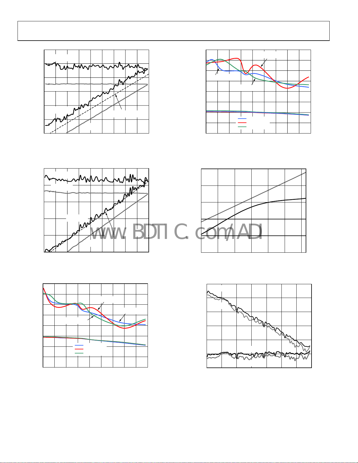
SFDR (dBFS)
100
80
SNR (dBFS)
60
40
SNR/SFDR (dBc AND dBFS)
20
0
–90 0–10–20–30–40–50–60–70–80
SFDR (dBc)
SNR (dBc)
INPUT AMPLITUDE (dBFS)
85dB REFERENCE L INE
Figure 28. AD9627-150 Single-Tone SNR/SFDR vs. Input Amplitude (A
= 2.4 MHz
with f
IN
100
SFDR (dBFS)
06571-028
)
IN
SNR/SFDR (dBc)
95
90
85
SFDR = +25°C
80
75
70
65
60
55
0440035030025020015010050
SFDR = –40°C
INPUT FREQ UENCY (MHz)
SFDR = +85°C
SNR = +25°C
SNR = +85°C
SNR = –40°C
Figure 31. AD9627-150 Single-Tone SNR/SFDR vs.
Input Frequ
2.5
) and Temperature with 1 V p-p Full Scale
ency (f
IN
50
06571-031
0.5
80
SNR (dBFS)
60
SFDR (dBc)
SNR (dBc)
INPUT AMPLITUDE (dBFS)
SNR/SFDR (dBc AND dBFS)
40
20
0
–90 0–10–20–30–40–50–60–70–80
Figure 29. AD9627-150 Single-Tone S
= 98.12 MHz
f
IN
95
90
85
80
75
70
SNR/SFDR (dBc)
65
60
55
04
SFDR = –40°C
SNR = +25°C
SNR = +85°C
SNR = –40°C
INPUT FREQ UENCY (MHz)
Figure 30. AD9627-150 Single-Tone SNR/SFDR vs.
Input Frequ
) and Temperature with 2 V p-p Full Scale
ency (f
IN
85dB REFERENCE LINE
NR/SFDR vs. Input Amplitude (A
SFDR = +85°C
SFDR = +25°C
25020015010050
50400350300
) with
IN
–3.0
–3.5
–4.0
GAIN ERROR (%F SR)
–4.5
–5.0
–40 806040
06571-029
TEMPERATURE ( °C)
GAIN
OFFSET
200–20
0.4
0.3
0.2
0.1
0
OFFSET ERROR (%FSR)
06571-032
Figure 32. AD9627-150 Gain and Offset vs. Temperature
0
SFDR (dBc)
–20
IMD3 (dBc)
–40
–60
–80
SFDR/IMD3 (dBc AND dBFS )
–100
–120
–90 –78 –66 –54 –42 –30 –18 –6
06571-030
Figure 33. AD9627-150 Two-Tone SFDR/IMD3 vs. Input Amplitude (A
with f
= 29.1 MHz, f
IN1
SFDR (dBFS)
IMD3 (dBFS)
INPUT AMPLI TUDE (dBFS)
= 32.1 MHz, fS = 150 MSPS
IN2
06571-033
)
IN
Rev. 0 | Page 22 of 76
Page 23
AD9627
www.BDTIC.com/ADI
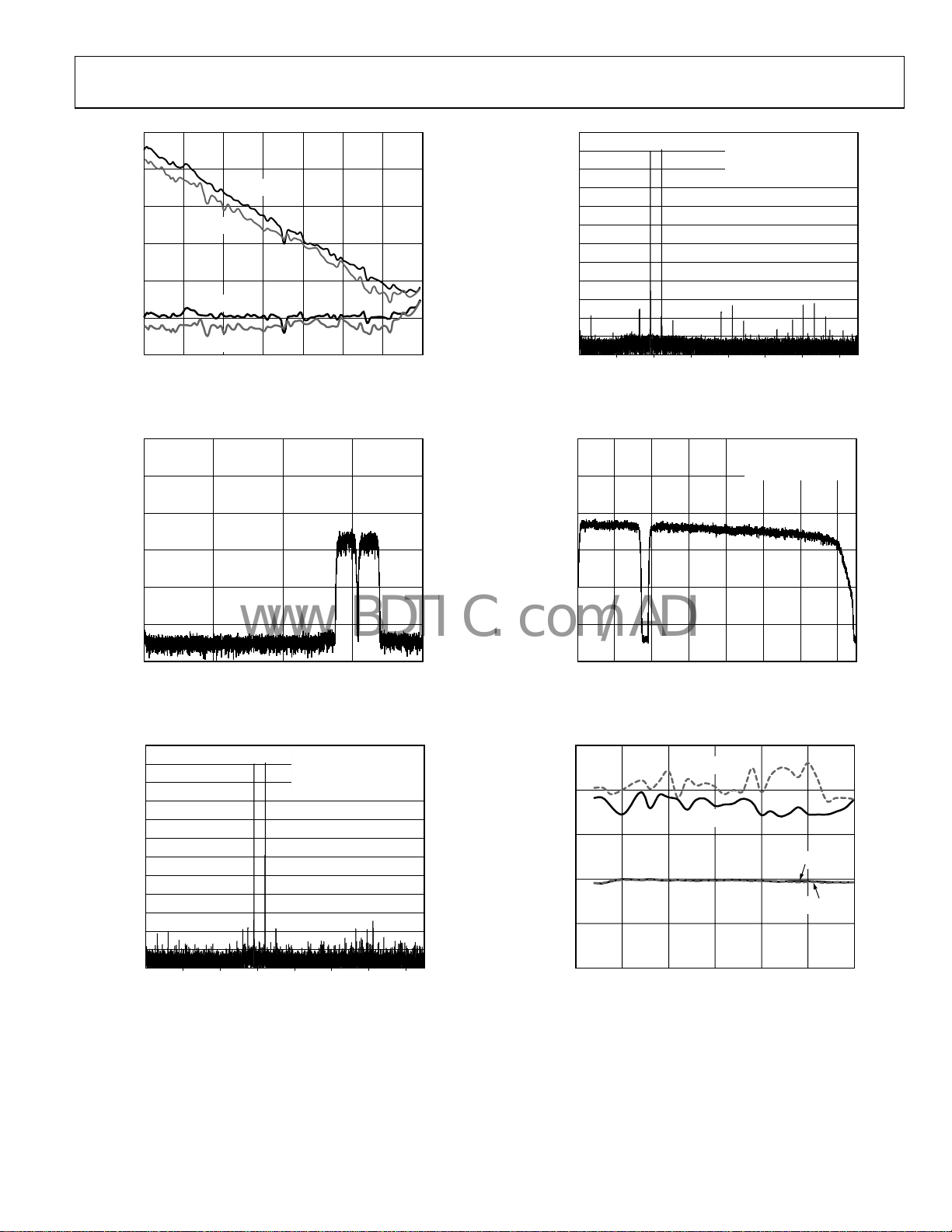
0
–20
SFDR (dBc)
–40
IMD3 (dBc)
–60
–20
–40
–60
0
150MSPS
169.1MHz @ –7dBF S
172.1MHz @ –7dBF S
SFDR = 83.8d Bc (90.8dBFS )
–80
SFDR/IMD3 (dBc AND dBFS )
–100
–120
–90 –78 –66 –54 –42 –30 –18 –6
SFDR (dBFS)
IMD3 (dBFS)
INPUT AMPLITUDE (dBFS)
Figure 34. AD9627-150 Two-Tone SFDR/IMD3 vs. Input Amplitude (A
= 169.1 MHz, f
with f
IN1
0
–20
–40
–60
–80
AMPLITUDE ( dBFS)
–100
–120
0 15.36 30.72 46.08 61. 44
= 172.1 MHz, fS = 150 MSPS
IN2
FREQUENCY (MHz )
Figure 35. AD9627-125, Two 64k WCDMA Carriers
= 170 MHz, fS = 122.88 MSPS
with f
IN
0
–20
150MSPS
29.1MHz @ –7dBF S
32.1MHz @ –7dBF S
SFDR = 86.1d Bc (93.1dBFS )
–80
AMPLITUDE ( dBFS)
–100
–120
07605040302010
06571-034
)
IN
06571-035
Figure 37. AD9627-150 Two-Tone FFT with f
0
–20
–40
–60
–80
AMPLITUDE ( dBFS)
–100
–120
07605040302010
FREQUENCY (MHz)
= 172.1 MHz
f
IN2
FREQUENCY (MHz )
= 169.1 MHz and
IN1
NPR = 61.5dBc
NOTCH @ 18.5MHz
NOTCH WIDT H = 3MHz
0
06571-037
0
06571-038
Figure 38. AD9627-150 Noise Power Ratio (NPR)
100
SFDR - SIDE B
90
–40
–60
–80
AMPLITUDE ( dBFS)
–100
–120
07
FREQUENCY (MHz)
Figu re 36. AD9627-150 Two-Tone FFT with f
= 29.1 MHz and f
IN1
605040302010
0
06571-036
= 32.1 MHz
IN2
Rev. 0 | Page 23 of 76
SFDR - SIDE A
SNR - SIDE B
SNR - SIDE A
SAMPLE RATE (MSPS)
SNR/SFDR (dBc)
80
70
60
50
0150125100755025
Figure 39. AD9627-150 Single-Tone SNR/SFDR vs. Sample Rate (f
with f
= 2.3 MHz
IN
06571-039
)
S
Page 24

AD9627
www.BDTIC.com/ADI
12
10
8
0.3 LSB rms
100
95
90
85
SFDR DCS ON
INL ERROR (LS B)
NUMBER OF HIT S (1M)
6
4
2
0
OUTPUT CODE
Figure 40. AD9627 Grounded Input Histogram
0.4
0.3
0.2
0.1
0
–0.1
–0.2
–0.3
–0.4
0 4096358430722560204815361024512
OUTPUT CODE
Figure 41. AD9627 INL with f
0.25
0.15
= 10.3 MHz
IN
80
75
SNR/SFDR (dBc)
N + 3N + 2N + 1NN – 1N – 2N – 3
06571-040
SNR DCS ON
70
65
60
20 806040
Figure 43. AD9627-150 SNR/SFDR vs. Duty Cycle with f
95
90
85
80
75
SNR/SFDR (dBc)
70
65
60
0.2 0.3 0. 4 0. 5 0.6 0.7 0.8 0.9 1.0 1.1 1. 2 1.3
06571-041
INPUT COMMON-MODE VOLTAGE (V)
SFDR DCS OFF
SNR DCS OFF
DUTY CYCLE (%)
SFDR
SNR
= 10.3 MHz
IN
06571-043
06571-044
Figure 44. AD9627-150 SNR/SFDR vs. Input Common Mode (VCM)
= 30 MHz
with f
IN
0.05
–0.05
DNL ERRO R (LSB)
–0.15
–0.25
0 4096358430722560204815361024512
Figure 42. AD9627 DNL with f
OUTPUT CODE
= 10.3 MHz
IN
06571-042
Rev. 0 | Page 24 of 76
Page 25

AD9627
www.BDTIC.com/ADI
THEORY OF OPERATION
The AD9627 dual ADC design can be used for diversity reception
of signals, where the ADCs are operating identically on the same
carrier but from two separate antennae. The ADCs can also be
operated with independent analog inputs. The user can sample
any f
/2 frequency segment from dc to 200 MHz, using appropriate
S
low-pass or band-pass filtering at the ADC inputs with little loss
in ADC performance. Operation to 450 MHz analog input is
permitted but occurs at the expense of increased ADC noise and
distortion.
In nondiversity applications, the AD9627 can be used as a base-
and or direct downconversion receiver, where one ADC is
b
used for I input data, and the other is used for Q input data.
Synchronizaton capability is provided to allow synchronized
g between multiple channels or multiple devices.
timin
Programming and control of the AD9627 are accomplished
usin
g a 3-bit SPI-compatible serial interface.
ADC ARCHITECTURE
The AD9627 architecture consists of a dual front-end sampleand-hold amplifier (SHA), followed by a pipelined, switched
capacitor ADC. The quantized outputs from each stage are
combined into a final 12-bit result in the digital correction logic.
The pipelined architecture permits the first stage to operate on
a new input sample and the remaining stages to operate on the
preceding samples. Sampling occurs on the rising edge of the clock.
Each stage of the pipeline, excluding the last, consists of a low
re
solution flash ADC connected to a switched capacitor digitalto-analog converter (DAC) and an interstage residue amplifier
(MDAC). The residue amplifier magnifies the difference between
the reconstructed DAC output and the flash input for the next
stage in the pipeline. One bit of redundancy is used in each stage
to facilitate digital correction of flash errors. The last stage simply
consists of a flash ADC.
The input stage of each channel contains a differential SHA that
ca
n be ac- or dc-coupled in differential or single-ended modes.
The output staging block aligns the data, corrects errors, and passes
the data to the output buffers. The output buffers are powered from
a separate supply, allowing adjustment of the output voltage swing.
During power-down, the output buffers go into a high impedance
state.
ANALOG INPUT CONSIDERATIONS
The analog input to the AD9627 is a differential switched
capacitor SHA that has been designed for optimum performance
while processing a differential input signal.
The clock signal alternatively switches the SHA between sample
m
ode and hold mode (see Figure 45). When the SHA is switched
to sample mode, the signal source must be capable of charging
in
the sample capacitors and settling within 1/2 of a clock cycle.
A small resistor in series with each input can help reduce the
p
eak transient current required from the output stage of the
driving source. A shunt capacitor can be placed across the
inputs to provide dynamic charging currents. This passive
network creates a low-pass filter at the ADC input; therefore,
the precise values are dependent on the application.
In intermediate frequency (IF) undersampling applications, any
sh
unt capacitors should be reduced. In combination with the
driving source impedance, the shunt capacitors limit the input
bandwidth. Refer to Application Note AN-742, Frequency
Domain Response of Switched-Capacitor ADCs; Application Note
AN-827, A Resonant Approach to Interfacing Amplifiers to
Switched-Capacitor ADCs; and the Analog Dialogue article,
“
Transformer-Coupled Front-End for Wideband A/D Converters,”
r more information on this subject (see www.analog.com).
fo
S
C
H
C
H
S
06571-045
VIN+
VIN–
C
PIN, PAR
C
PIN, PAR
Figure 45. Switched-Capac
S
S
C
S
H
C
S
itor SHA Input
For best dynamic performance, the source impedances driving
VIN+ and VIN− should be matched.
An internal differential reference buffer creates positive and
ne
gative reference voltages that define the input span of the ADC
core. The span of the ADC core is set by this buffer to 2 × VREF.
Input Common Mode
The analog inputs of the AD9627 are not internally dc biased.
In ac-coupled applications, the user must provide this bias
externally. Setting the device so that V
= 0.55 × AVDD
CM
is recommended for optimum performance, but the device
functions over a wider range with reasonable performance
(see
Figure 44). An on-board common-mode voltage reference
cluded in the design and is available from the CML pin.
is in
Optimum performance is achieved when the common-mode
voltage of the analog input is set by the CML pin voltage
(typically 0.55 × AVDD). The CML pin must be decoupled to
ground by a 0.1 µF capacitor, as described in the
formation section.
In
Applications
Differential Input Configurations
Optimum performance is achieved while driving the AD9627 in a
differential input configuration. For baseband applications, the
AD8138, ADA4937-2, and ADA4938-2 differential drivers provide
exce
llent performance and a flexible interface to the ADC.
Rev. 0 | Page 25 of 76
Page 26

AD9627
Ω
A
V
F
F
V
www.BDTIC.com/ADI
The output common-mode voltage of the AD8138 is easily set
with the CML pin of the AD9627 (see Figure 46), and the driver
ca
n be configured in a Sallen-Key filter topology to provide
band limiting of the input signal.
499
1V p-p
0.1µF
49.9Ω
499Ω
AD8138
523Ω
499Ω
Figure 46. Differential Input Configuration Using the AD8138
R
C
R
VIN+
AD9627
VIN–
AVDD
CML
For baseband applications where SNR is a key parameter,
differential transformer coupling is the recommended input
configuration. An example is shown in Figure 47. To bias the
a
nalog input, the CML voltage can be connected to the center
tap of the secondary winding of the transformer.
R
2V p-p
49.9Ω
0.1µF
C
R
Figure 47. Differential Transformer-Coupled Configuration
VIN+
AD9627
VIN–
CML
06571-047
The signal characteristics must be considered when selecting
a transformer. Most RF transformers saturate at frequencies
below a few megahertz (MHz). Excessive signal power can also
cause core saturation, which leads to distortion.
At input frequencies in the second Nyquist zone and above, the
n
oise performance of most amplifiers is not adequate to achieve
the true SNR performance of the AD9627. For applications where
SNR is a key parameter, differential double balun coupling is the
recommended input configuration (see
2V p-p
Figure 49).
0.1µ
A
0.1µ
S
SP
P
0.1µF
Figure 49. Differential Double Balun Input Configuration
CC
06571-046
An alternative to using a transformer-coupled input at frequencies
in t
he second Nyquist zone is to use the AD8352 differential driver.
An example is shown in
r more information.
fo
Figure 50. See the AD8352 data sheet
In any configuration, the value of Shunt Capacitor C is dependent
o
n the input frequency and source impedance and may need to
be reduced or removed. Tab l e 1 3 displays recommended values to
s
et the RC network. However, these values are dependent on the
input signal and should be used only as a starting guide.
Table 13. Example RC Network
R Series
Frequency Range (MHz)
(Ω Each)
C Differential (pF)
0 to 70 33 15
70 to 200 33 5
200 to 300 15 5
>300 15 Open
Single-Ended Input Configuration
A single-ended input can provide adequate performance in cost
sensitive applications. In this configuration, SFDR and distortion
performance degrade due to the large input common-mode swing.
If the source impedances on each input are matched, there should
be little effect on SNR performance.
gle-ended input configuration.
sin
10µF
0.1µF
0.1µF
Figure 48. Single-Ended Input Configuration
VIN+
VIN–
25Ω
25Ω
0.1µF
1V p-p
49.9Ω
10µF
R
C
R
1kΩ
1kΩ
AVD D
1kΩ
1kΩ
AD9627
Figure 48 shows a typical
DD
R
C
R
CML
06571-049
VIN+
AD9627
VIN–
06571-048
0.1µF
0Ω
ANALOG INPUT
R
C
D
ANALOG INPUT
0.1µF
Figure 50. Differential Input Configuration Using the AD8352
16
1
2
R
D
G
3
4
5
0Ω
8, 13
11
AD8352
10
14
0.1µF
Rev. 0 | Page 26 of 76
0.1µF
0.1µF
200Ω
200Ω
0.1µF
R
C
R
0.1µF
VIN+
AD9627
VIN–
CML
06571-050
Page 27

AD9627
www.BDTIC.com/ADI
VOLTAGE REFERENCE
A stable and accurate voltage reference is built into the AD9627.
The input range can be adjusted by varying the reference voltage
applied to the AD9627, using either the internal reference or an
externally applied reference voltage. The input span of the ADC
tracks reference voltage changes linearly. The various reference
modes are summarized in the sections that follow. The
Deco
upling section describes the best practices PCB layout of
t
he reference.
Internal Reference Connection
A comparator within the AD9627 detects the potential at the
SENSE pin and configures the reference into four possible
modes, which are summarized in Tabl e 14. If SENSE is grounded,
t
he reference amplifier switch is connected to the internal resistor
divider (see
ENSE pin to VREF switches the reference amplifier output
S
Figure 51), setting VREF to 1.0 V. Connecting the
to the SENSE pin, completing the loop and providing a 0.5 V
reference output.
VIN+A/ VIN+B
VIN–A/VIN–B
ADC
CORE
VREF
0.1µF1.0µF
SENSE
SELECT
LOGIC
0.5V
Reference
The input range of the ADC always equals twice the voltage at
t
he reference pin for either an internal or an external reference.
VIN+A/VIN+ B
VIN–A/ VIN–B
ADC
CORE
VREF
0.1µF1.0µF
Figure 52. Programmable Reference Configuration
R2
SENSE
R1
SELECT
LOGIC
0.5V
AD9627
6571-052
If the internal reference of the AD9627 is used to drive multiple
converters to improve gain matching, the loading of the reference
by the other converters must be considered. Figure 53 shows
ow the internal reference voltage is affected by loading.
h
0
VREF = 0.5V
–0.25
VREF = 1.0V
–0.50
–0.75
AD9627
Figure 51. Internal Reference Configuration
6571-051
If a resistor divider is connected external to the chip, as shown
in Figure 52, the switch again sets to the SENSE pin. This puts
he reference amplifier in a noninverting mode with the VREF
t
output defined as follows:
R2
⎞
⎛
VREF 15.0
+×=
⎟
⎜
R1
⎠
⎝
–1.00
REFERENCE VOL TAGE ERROR ( %)
–1.25
02
0.5 1.0 1.5
LOAD CURRENT (mA)
Figure 53. VREF Accuracy vs. Load
Table 14. Reference Configuration Summary
Selected Mode SENSE Voltage Resulting VREF (V) Resulting Differential Span (V p-p)
External Reference AVDD N/A 2 × external reference
Internal Fixed Reference VREF 0.5 1.0
R2
Programmable Reference 0.2 V to VREF
⎛
⎜
⎝
⎞
(see Figure 52)
+×
10.5
⎟
R1
⎠
2 × VREF
Internal Fixed Reference AGND to 0.2 V 1.0 2.0
Rev. 0 | Page 27 of 76
.0
6571-053
Page 28

AD9627
www.BDTIC.com/ADI
External Reference Operation
The use of an external reference may be necessary to enhance
the gain accuracy of the ADC or improve thermal drift characteristics. Figure 54 shows the typical drift characteristics of the
nternal reference in 1.0 V mode.
i
2.5
2.0
1.5
1.0
0.5
0
–0.5
–1.0
–1.5
REFERENCE VOL TAGE ERROR ( mV)
–2.0
–2.5
–40
–200 20406080
TEMPERATURE (° C)
Figure 54. Typical VREF Drift
06571-054
When the SENSE pin is tied to AVDD, the internal reference is
disabled, allowing the use of an external reference. An internal
reference buffer loads the external reference with an equivalent
6 kΩ load (see Figure 15). The internal buffer generates the
ositive and negative full-scale references for the ADC core.
p
Therefore, the external reference must be limited to a maximum
of 1.0 V.
CLOCK INPUT CONSIDERATIONS
For optimum performance, the AD9627 sample clock inputs,
CLK+ and CLK−, should be clocked with a differential signal.
The signal is typically ac-coupled into the CLK+ and CLK− pins
via a transformer or capacitors. These pins are biased internally
(see Figure 55) and require no external bias.
AVDD
1.2V
CLK–CLK+
2pF 2pF
6571-055
Figure 55. Equivalent Clock Input Circuit
Clock Input Options
The AD9627 has a very flexible clock input structure. Clock input
can be a CMOS, LVDS, LVPECL, or sine wave signal. Regardless of
the type of signal being used, clock source jitter is of the most
concern, as described in the
Jitter Considerations section.
Figure 56 and Figure 57 show two preferred methods for clocking
th
e AD9627 (at clock rates up to 625 MHz). A low jitter clock
source is converted from a single-ended signal to a differential
signal using either an RF balun or an RF transformer.
Rev. 0 | Page 28 of 76
The RF balun configuration is recommended for clock
f
requencies between 125 MHz and 625 MHz, and the RF
transformer is recommended for clock frequencies from 10 MHz
to 200 MHz. The back-to-back Schottky diodes across the
transformer/balun secondary limit clock excursions into the
AD9627 to approximately 0.8 V p-p differential.
This helps prevent the large voltage swings of the clock from
f
eeding through to other portions of the AD9627 while preserving
the fast rise and fall times of the signal that are critical to a low
jitter performance.
XFMR
0.1µF
®
0.1µF0.1µF
0.1µF
0.1µF1nF
0.1µF
SCHOTTKY
DIODES:
HSMS2822
SCHOTTKY
DIODES:
HSMS2822
CLK+
AD9627
CLK–
CLK+
ADC
AD9627
CLK–
ADC
06571-057
Mini-Circuits
ADT1–1WT, 1:1Z
CLOCK
INPUT
50Ω
100Ω
Figure 56. Transformer-Coupled Differential Clock (Up to 200 MHz)
CLOCK
INPUT
50Ω
1nF
Figure 57. Balun-Coupled Differential Clock (Up to 625 MHz)
If a low jitter clock source is not available, another option is to
ac couple a differential PECL signal to the sample clock input
pins, as shown in Figure 58. The AD9510/AD9511/AD9512/
AD9513/AD9514/AD9515/AD9516 clock drivers offer excellent
tter performance.
ji
CLOCK
INPUT
CLOCK
INPUT
0.1µF
0.1µF
50kΩ 50kΩ
AD951x
PECL DRIVER
0.1µF
CLK+
100Ω
0.1µF
240Ω240Ω
ADC
AD9627
CLK–
Figure 58. Differential PECL Sample Clock (Up to 625 MHz)
A third option is to ac-couple a differential LVDS signal to the
sample clock input pins, as shown in Figure 59. The AD9510/
AD9511/AD9512/AD9513/AD9514/AD9515/AD9516 clock
rivers offer excellent jitter performance.
d
CLOCK
INPUT
CLOCK
INPUT
50kΩ 50kΩ
0.1µF
0.1µF
AD951x
LVDS DRIVER
Figure 59. Differential LVDS Sample Clock (Up to 625 MHz)
0.1µF
100Ω
0.1µF
CLK+
ADC
AD9627
CLK–
06571-056
06571-058
06571-059
Page 29

AD9627
www.BDTIC.com/ADI
In some applications, it may be acceptable to drive the sample
clock inputs with a single-ended CMOS signal. In such applications, the CLK+ pin should be driven directly from a CMOS gate,
and the CLK− pin should be bypassed to ground with a 0.1 F
capacitor in parallel with a 39 k resistor (see
Figure 60).
CLK+ can be driven directly from a CMOS gate. Although the
CLK+ in
put circuit supply is AVDD (1.8 V), this input is designed
to withstand input voltages of up to 3.6 V, making the selection
of the drive logic voltage very flexible.
V
CC
0.1µF
1kΩ
V
CC
1kΩ
1kΩ
1kΩ
AD951x
CMOS DRIVE R
AD951x
CMOS DRIVE R
CLOCK
INPUT
Figure 60. Single-Ended 1.8 V CMOS Sample Clock (Up to 150 MSPS)
CLOCK
INPUT
Figure 61. Single-Ended 3.3 V CMOS Sample Clock (Up to 150 MSPS)
1
50Ω
1
50Ω RESISTO R IS OP TIONAL .
0.1µF
1
50Ω
1
50Ω RESISTOR IS OPTIONAL.
0.1µF
OPTIONAL
100Ω
OPTIONAL
100Ω
39kΩ
0.1µF
0.1µF
0.1µF
CLK+
ADC
AD9627
CLK–
CLK+
ADC
AD9627
CLK–
Input Clock Divider
The AD9627 contains an input clock divider with the ability to
divide the input clock by integer values between 1 and 8. If a
divide ratio other than 1 is selected, the duty cycle stabilizer is
automatically enabled.
The AD9627 clock divider can be synchronized using the external
YNC input. Bit 1 and Bit 2 of Register 0x100 allow the clock
S
divider to be resynchronized on every SYNC signal or only on
the first SYNC signal after the register is written. A valid SYNC
causes the clock divider to reset to its initial state. This synchronization feature allows multiple parts to have their clock dividers
aligned to guarantee simultaneous input sampling.
Clock Duty Cycle
Typical high speed ADCs use both clock edges to generate
a variety of internal timing signals and, as a result, may be
sensitive to clock duty cycle. Commonly, a ±5% tolerance is
required on the clock duty cycle to maintain dynamic
performance characteristics.
The AD9627 contains a duty cycle stabilizer (DCS) that retimes
t
he nonsampling (falling) edge, providing an internal clock
signal with a nominal 50% duty cycle. This allows the user to
provide a wide range of clock input duty cycles without affecting
the performance of the AD9627. Noise and distortion performance
are nearly flat for a wide range of duty cycles with the DCS on,
as shown in
Figure 43.
Rev. 0 | Page 29 of 76
06571-060
06571-061
Jitter in the rising edge of the input is still of paramount concern
a
nd is not easily reduced by the internal stabilization circuit.
The duty cycle control loop does not function for clock rates
less than 20 MHz nominally. The loop has a time constant
associated with it thatmust be considered where the clock rate
can change dynamically. A wait time of 1.5 µs to 5 µs is required
after a dynamic clock frequency increase or decrease before the
DCS loop is relocked to the input signal. During the time period
that the loop is not locked, the DCS loop is bypassed, and internal
device timing is dependent on the duty cycle of the input clock
signal. In such applications, it may be appropriate to disable the
duty cycle stabilizer. In all other applications, enabling the DCS
circuit is recommended to maximize ac performance.
Jitter Considerations
High speed, high resolution ADCs are sensitive to the quality
of the clock input. The degradation in SNR from the low
frequency SNR (SNR
to jitter (t
SNR
) can be calculated by
JRMS
= −10 log[(2π × f
HF
) at a given input frequency (f
LF
× t
INPUT
)2 + 10 ]
JRMS
INPUT
) due
)10/(LFSNR−
In the equation, the rms aperture jitter represents the clock input
jitter specification. IF undersampling applications are particularly
sensitive to jitter, as illustrated in
75
70
MEASURED
65
60
SNR (dBc)
55
50
45
1 10 100 1000
Figure 62. SNR vs. Input Frequency and Jitter
Figure 62.
INPUT FREQ UENCY (MHz)
0.05ps
0.20ps
0.5ps
1.0ps
1.50ps
2.00ps
2.50ps
3.00ps
06571-062
The clock input should be treated as an analog signal in cases
where aperture jitter may affect the dynamic range of the AD9627.
Power supplies for clock drivers should be separated from the
ADC output driver supplies to avoid modulating the clock
signal with digital noise. Low jitter, crystal-controlled oscillators
make the best clock sources. If the clock is generated from another
type of source (by gating, dividing, or another method), it should
be retimed by the original clock at the last step.
Refer to Application Note AN-501 and Application Note AN-756
(see www.analog.com) for more information about jitter perform-
anc
e as it relates to ADCs.
Page 30

AD9627
www.BDTIC.com/ADI
POWER DISSIPATION AND STANDBY MODE
As shown in Figure 63 through Figure 66, the power dissipated
by the AD9627 is proportional to its sample rate. In CMOS
output mode, the digital power dissipation is determined
primarily by the strength of the digital drivers and the load
on each output bit.
The maximum DRVDD current (I
I
DRVDD
where N is t
= V
DRVDD
× C
LOAD
× f
CLK
he number of output bits (26, in the case of the
AD9627, with the fast detect output pins disabled).
This maximum current occurs when every output bit switches on
e
very clock cycle, that is, a full-scale square wave at the Nyquist
frequency of f
/2. In practice, the DRVDD current is
CLK
established by the average number of output bits switching,
which is determined by the sample rate and the characteristics
of the analog input signal.
Reducing the capacitive load presented to the output drivers can
mize digital power consumption. The data in Figure 63 was
mini
en using the same operating conditions as those used for the
tak
Typical Performance Characteristics, with a 5 pF load on each
driver.
output
1.25
1.00
0.75
0.50
TOTAL POWER (W)
0.25
0
0255075100125150
TOTAL POWER
I
DVDD
SAMPLE RATE (MSPS)
Figure 63. AD9627-150 Power and Current vs. Sample Rate
1.25
1.00
0.75
0.50
TOTAL POWER (W)
0.25
0
0 25 50 75 100 125
Figure 64. AD9627-125 Power and Current vs. Sample Rate
I
AVDD
TOTAL POWER
I
DVDD
SAMPLE RATE (MSPS)
) can be calculated as
DRVDD
× N
I
AVDD
I
DRVDD
I
DRVDD
0.5
0.4
0.3
0.2
SUPPLY CURRENT (A)
0.1
0
0.5
0.4
0.3
0.2
SUPPLY CURRENT (A)
0.1
0
Rev. 0 | Page 30 of 76
1.00
I
0.75
0.50
TOTAL POWER (W)
0.25
I
DVDD
0
0255075100
AVDD
TOTAL POWER
SAMPLE RATE (MSPS)
I
DRVDD
0.4
0.3
0.2
0.1
0
SUPPLY CURRENT (A)
06571-065
Figure 65. AD9627-105 Power and Current vs. Sample Rate
0.75
I
AVDD
0.50
TOTAL POWER
0.25
TOTAL POWER (W)
I
I
DVDD
0
0 20406080
SAMPLE RATE (MSPS)
DRVDD
Figure 66. AD9627-80 Power and Current vs. Sample Rate
0.3
0.2
0.1
0
SUPPLY CURRENT (A)
06571-066
By asserting PDWN (either through the SPI port or by asserting
the PDWN pin high), the AD9627 is placed in power-down
mode. In this state, the ADC typically dissipates 2.5 mW.
During power-down, the output drivers are placed in a high
06571-063
impedance state. Asserting the PDWN pin low returns the
AD9627 to its normal operating mode. Note that PDWN is
referenced to the digital output driver supply (DRVDD) and
should not exceed that supply voltage.
Low power dissipation in power-down mode is achieved by
utting down the reference, reference buffer, biasing networks,
sh
and clock. Internal capacitors are discharged when entering powerdown mode and then must be recharged when returning to normal
operation. As a result, wake-up time is related to the time spent
in power-down mode, and shorter power-down cycles result in
proportionally shorter wake-up times.
When using the SPI port interface, the user can place the ADC
in p
ower-down mode or standby mode. Standby mode allows
the user to keep the internal reference circuitry powered when
faster wake-up times are required. See the Memory Map Register
scription
De
06571-064
s section for more details.
Page 31

AD9627
www.BDTIC.com/ADI
DIGITAL OUTPUTS
The AD9627 output drivers can be configured to interface with
1.8 V to 3.3 V CMOS logic families by matching DRVDD to the
digital supply of the interfaced logic. The AD9627 can also be
configured for LVDS outputs using a DRVDD supply voltage
of 1.8 V.
In CMOS output mode, the output drivers are sized to provide
s
ufficient output current to drive a wide variety of logic families.
However, large drive currents tend to cause current glitches on
the supplies that may affect converter performance.
Applications requiring the ADC to drive large capacitive loads
r large fanouts may require external buffers or latches.
o
The output data format can be selected for either offset binary
r twos complement by setting the SCLK/DFS pin when operating
o
in the external pin mode (see
As detailed in A
Speed ADCs via SPI, the data format can be selected for offset
binary, twos complement, or gray code when using the SPI control.
Table 15. SCLK/DFS Mode Selection (External Pin Mode)
Voltage at Pin SCLK/DFS SDIO/DCS
AGND (default) Offset binary DCS disabled
AVDD Twos complement DCS enabled
pplication Note AN-877, Interfacing to High
Table 1 5).
Digital Output Enable Function (OEB)
The AD9627 has a flexible three-state ability for the digital output
pins. The three-state mode is enabled using the SMI SDO/OEB
pin or through the SPI interface. If the SMI SDO/OEB pin is low,
the output data drivers are enabled. If the SMI SDO/OEB pin is
high, the output data drivers are placed in a high impedance state.
This OEB function is not intended for rapid access to the data
bus. Note that OEB is referenced to the digital output driver supply
(DRVDD) and should not exceed that supply voltage.
When using the SPI interface, the data and fast detect outputs
f each channel can be independently three-stated by using the
o
output enable bar bit in Register 0x14.
TIMING
The AD9627 provides latched data with a pipeline delay of
12 clock cycles. Data outputs are available one propagation
delay (t
The length of the output data lines and loads placed on them
s
hould be minimized to reduce transients within the AD9627.
These transients can degrade converter dynamic performance.
The lowest typical conversion rate of the AD9627 is 10 MSPS.
A
Data Clock Output (DCO)
The AD9627 provides two data clock output (DCO) signals
intended for capturing the data in an external register. The data
outputs are valid on the rising edge of DCO, unless the DCO clock
polarity has been changed via the SPI. See Figure 2 and Figure 3
fo
) after the rising edge of the clock signal.
PD
t clock rates below 10 MSPS, dynamic performance can degrade.
r a graphical timing description.
Table 16. Output Data Format
Input (V) Condition (V) Offset Binary Output Mode Twos Complement Mode OR
VIN+ − VIN− < −VREF − 0.5 LSB 0000 0000 0000 1000 0000 0000 1
VIN+ − VIN− = −VREF 0000 0000 0000 1000 0000 0000 0
VIN+ − VIN− = 0 1000 0000 0000 0000 0000 0000 0
VIN+ − VIN− = +VREF − 1.0 LSB 1111 1111 1111 0111 1111 1111 0
VIN+ − VIN− > +VREF − 0.5 LSB 1111 1111 1111 0111 1111 1111 1
Rev. 0 | Page 31 of 76
Page 32

AD9627
www.BDTIC.com/ADI
ADC OVERRANGE AND GAIN CONTROL
In receiver applications, it is desirable to have a mechanism to
reliably determine when the converter is about to be clipped.
The standard overflow indicator provides after-the-fact information on the state of the analog input that is of limited usefulness.
Therefore, it is helpful to have a programmable threshold below
full scale that allows time to reduce the gain before the clip
actually occurs. In addition, because input signals can have
significant slew rates, latency of this function is of major concern.
Highly pipelined converters can have significant latency. A good
compromise is to use the output bits from the first stage of the
ADC for this function. Latency for these output bits is very low,
and overall resolution is not highly significant. Peak input signals
are typically between full scale and 6 dB to 10 dB below full
scale. A 3-bit or 4-bit output provides adequate range and
resolution for this function.
Using the SPI port, the user can provide a threshold above which
n overrange output is active. As long as the signal is below that
a
threshold, the output should remain low. The fast detect outputs
can also be programmed via the SPI port so that one of the pins
functions as a traditional overrange pin for customers who
currently use this feature. In this mode, all 12 bits of the converter
are examined in the traditional manner, and the output is high for
the condition normally defined as overflow. In either mode, the
magnitude of the data is considered in the calculation of the
condition (but the sign of the data is not considered). The threshold
detection responds identically to positive and negative signals
outside the desired range (magnitude).
FAST DETECT OVERVIEW
The AD9627 contains circuitry to facilitate fast overrange detection, allowing very flexible external gain control implementations.
Each ADC has four fast detect (FD) output pins that are used
to output information about the current state of the ADC input
level. The function of these pins is programmable via the fast detect
mode select bits and the fast detect enable bits in Register 0x104,
allowing range information to be output from several points in
the internal datapath. These output pins can also be set up to
indicate the presence of overrange or underrange conditions,
according to programmable threshold levels.
nfigurations available for the fast detect pins.
six co
Tabl e 17 shows the
Table 17. Fast Detect Mode Select Bits Settings
Fast Detect
Mode Select Bits
(Register 0x104[3:1])
000
001
010
011
100 OR C_UT F_UT F_LT
101 OR F_UT IG DG
1
The fast detect pins are FD0A/FD0B to FD9A/FD9B for the CMOS mode
configuration and FD0+/FD0− to FD9+/FD9− for the LVDS mode
configuration.
2
See the ADC Overrange (OR) and Gain Switching sections for more
information about OR, C_UT, F_UT, F_LT, IG, and DG.
Information Presented on
Fast Detect (FD) Pins of Each ADC
FD[3] FD[2] FD[1] FD[0]
ADC fast magnitude
(see Tab le 18)
ADC fast magnitude
(see Tab le 19)
ADC fast magnitude
ee Table 20)
(s
ADC fast magnitude
ee Table 20)
(s
OR F_LT
C_UT F_LT
1, 2
OR
ADC FAST MAGNITUDE
When the fast detect output pins are configured to output the ADC
fast magnitude (that is, when the fast detect mode select bits are
set to 0b000), the information presented is the ADC level from
an early converter stage with a latency of only two clock cycles
(when in CMOS output mode). Using the fast detect output pins
in this configuration provides the earliest possible level indication
information. Because this information is provided early in the
datapath, there is significant uncertainty in the level indicated.
The nominal levels, along with the uncertainty indicated by the
ADC fast magnitude, are shown in
Table 18. ADC Fast Magnitude Nominal Levels with Fast Detect
Mode Select Bits = 000
ADC Fast
Magnitude on
FD[3:0] Pins
0000 <−24 Minimum to −18.07
0001 −24 to −14.5 −30.14 to −12.04
0010 −14.5 to −10 −18.07 to −8.52
0011 −10 to −7 −12.04 to −6.02
0100 −7 to −5 −8.52 to −4.08
0101 −5 to −3.25 −6.02 to −2.5
0110 −3.25 to −1.8 −4.08 to −1.16
0111 −1.8 to −0.56 −2.5 to FS
1000 −0.56 to 0 −1.16 to 0
Nominal Input
Magnitude
Below FS (dB)
Tabl e 18 .
Nominal Input
Magnitude
Unc
ertainty (dB)
Rev. 0 | Page 32 of 76
Page 33

AD9627
www.BDTIC.com/ADI
When the fast detect mode select bits are set to 0b001, 0b010, or
0b011, a subset of the fast detect output pins is available. In these
modes, the fast detect output pins have a latency of six clock cycles.
Tabl e 1 9 shows the corresponding ADC input levels when the
fas
t detect mode select bits are set to 0b001 (that is, when ADC fast
magnitude is presented on the FD[3:1] pins).
Table 19. ADC Fast Magnitude Nominal Levels with
Fast Detect Mode Select Bits = 001
Nominal Input
ADC Fast Magnitude
on FD[3:1] Pins
000 <−24 Minimum to −18.07
001 −24 to −14.5 −30.14 to −12.04
010 −14.5 to −10 −18.07 to −8.52
011 −10 to −7 −12.04 to −6.02
100 −7 to −5 −8.52 to −4.08
101 −5 to −3.25 −6.02 to −2.5
110 −3.25 to −1.8 −4.08 to −1.16
111 −1.8 to 0 −2.5 to 0
Magnitude
Be
low FS (dB)
Nominal Input
Magnitude
Uncertainty (dB)
When the fast detect mode select bits are set to 0b010 or 0b011
(that is, when ADC fast magnitude is presented on the FD[3:2]
pins), the LSB is not provided. The input ranges for this mode
are shown in Ta ble 20 .
Table 20. ADC Fast Magnitude Nominal Levels with
Fast Detect Mode Select Bits = 010 or 011
ADC Fast
Magnitude on
FD[2:1] Pins
00 <−14.5 Minimum to −12.04
01 −14.5 to −7 −18.07 to −6.02
10 −7 to −3.25 −8.52 to −2.5
11 −3.25 to 0 −4.08 to 0
Nominal Input
Magnitude
Below FS (dB)
Nominal Input
Magnitude
Uncertainty (dB)
ADC OVERRANGE (OR)
The ADC overrange indicator is asserted when an overrange is
detected on the input of the ADC. The overrange condition is
determined at the output of the ADC pipeline and, therefore, is
subject to a latency of 12 ADC clock cycles. An overrange at the
input is indicated by this bit 12 clock cycles after it occurs.
GAIN SWITCHING
The AD9627 includes circuitry that is useful in applications either
where large dynamic ranges exist or where gain ranging converters
are employed. This circuitry allows digital thresholds to be set
such that an upper threshold and a lower threshold can be
programmed. Fast detect mode select bit = 010 through fast
detect mode select bit = 101 support various combinations of the
gain switching options.
One such use is to detect when an ADC is about to reach full
s
cale with a particular input condition. The result is to provide
an indicator that can be used to quickly insert an attenuator that
prevents ADC overdrive.
Coarse Upper Threshold (C_UT)
The coarse upper threshold indicator is asserted if the ADC fast
magnitude input level is greater than the level programmed in
the coarse upper threshold register (Address 0x105[2:0]). This
value is compared with the ADC Fast Magnitude Bits[2:0]. The
coarse upper threshold output is output two clock cycles after the
level is exceeded at the input and, therefore, it provides a fast
indication of the input signal level. The coarse upper threshold
levels are shown in
a
minimum of two ADC clock cycles or until the signal drops
Tabl e 2 1 . This indicator remains asserted for
below the threshold level.
Table 21. Coarse Upper Threshold Levels
C_UT Is Active When Signal
Coarse Upper Threshold
Register 0x105[2:0]
000 <−24
001 −24
010 −14.5
011 −10
100 −7
101 −5
110 −3.25
111 −1.8
Magnitude B
Is Greater Than (dB)
elow FS
Fine Upper Threshold (F_UT)
The fine upper threshold indicator is asserted if the input
magnitude exceeds the value programmed in the fine upper
threshold register located in Register 0x106 and Register 0x107.
The 13-bit threshold register is compared with the signal magnitude at the output of the ADC. This comparison is subject to the
ADC clock latency but is accurate in terms of the converter
resolution. The fine upper threshold magnitude is defined by
the following equation:
13
dBFS = 20 log(Th
reshold Magnitude/2
)
Fine Lower Threshold (F_LT)
The fine lower threshold indicator is asserted if the input
magnitude is less than the value programmed in the fine lower
threshold register located at Register 0x108 and Register 0x109.
The fine lower threshold register is a 13-bit register that is
compared with the signal magnitude at the output of the ADC.
This comparison is subject to ADC clock latency but is accurate
in terms of the converter resolution. The fine lower threshold
magnitude is defined by the following equation:
dBFS = 20 log(Th
reshold Magnitude/2
13
)
The operation of the fine upper threshold indicators and fine
wer threshold indicators is shown in Figure 67.
lo
Rev. 0 | Page 33 of 76
Page 34

AD9627
www.BDTIC.com/ADI
Increment Gain (IG) and Decrement Gain (DG)
The increment gain and decrement gain indicators are intended
to be used together to provide information to enable external
gain control. The decrement gain indicator works in conjunction
with the coarse upper threshold bits, asserting when the input
magnitude is greater than the 3-bit value in the coarse upper
threshold register (Address 0x105). The increment gain indicator,
similarly, corresponds to the fine lower threshold bits, except
that it is asserted only if the input magnitude is less than the
value programmed in the fine lower threshold register after the
dwell time elapses. The dwell time is set by the 16-bit dwell time
value located at Address 0x10A and Address 0x10B and is set in
units of ADC input clock cycles ranging from 1 to 65,535. The
fine lower threshold register is a 13-bit register that is compared
TIMER RESET BY
RISE ABOVE F_LT
with the magnitude at the output of the ADC. This comparison
is subject to the ADC clock latency but allows a finer, more
accurate comparison. The fine upper threshold magnitude is
defined by the following equation:
dBFS = 20 log(Th
reshold Magnitude/2
13
)
The decrement gain output works from the ADC fast detect
pins, providing a fast indication of potential overrange
output
conditions. The increment gain uses the comparison at the
output of the ADC, requiring the input magnitude to remain
below an accurate, programmable level for a predefined period
before signaling external circuitry to increase the gain.
The operation of the increment gain output and the decrement
ga
DWELL TIME
in output is shown in
UPPER THRESHOL D (COARSE OR F INE)
Figure 67.
FINE LOWER THRESHOL D
C_UT OR F _UT*
F_LT
DG
IG
*C_UT AND F_UT DIFFER ONLY I N ACCURACY AND LATENCY.
NOTE: OUT PUTS FO LLOW T HE INSTANTANEOUS SIGNAL LEVEL AND NOT THE ENVE LOPE BUT ARE GUARANTEED ACTI VE FOR A MI NIMUM OF 2 ADC CLOCK CYCLE S.
Figure 67. Threshold Settings for C_UT
, F_UT, IG, DG, and F_LT
DWELL TIME
TIMER COMPLETES BEFORE
SIGNAL RI SES ABOVE F_LT
6571-067
Rev. 0 | Page 34 of 76
Page 35

AD9627
www.BDTIC.com/ADI
SIGNAL MONITOR
The signal monitor block provides additional information
about the signal being digitized by the ADC. The signal monitor
computes the rms input magnitude, the peak magnitude,
and/or the number of samples by which the magnitude exceeds
a particular threshold. Together, these functions can be used to
gain insight into the signal characteristics and to estimate the
peak/average ratio or even the shape of the complementary
cumulative distribution function (CCDF) curve of the input signal.
This information can be used to drive an AGC loop to optimize
the range of the ADC in the presence of real-world signals.
The signal monitor result values can be obtained from the part by
r
eading back internal registers at Address 0x116 to Address 0x11B,
using the SPI port or the signal monitor SPORT output. The output
contents of the SPI-accessible signal monitor registers are set via
the two signal monitor mode bits of the signal monitor control
register. Both ADC channels must be configured for the same
signal monitor mode. Separate SPI-accessible, 20-bit signal monitor
result (SMR) registers are provided for each ADC channel. Any
combination of the signal monitor functions can also be output
to the user via the serial SPORT interface. These outputs are
enabled using the peak detector output enable, the rms magnitude
output enable, and the threshold crossing output enable bits in
the signal monitor SPORT control register.
For each signal monitor measurement, a programmable signal
itor period register (SMPR) controls the duration of the
mon
measurement. This time period is programmed as the number of
input clock cycles in a 24-bit signal monitor period register
located at Address 0x113, Address 0x114, and Address 0x115.
This register can be programmed with a period from 128 samples
24
to 16.78 (2
) million samples.
Because the dc offset of the ADC can be significantly larger
han the signal of interest (affecting the results from the signal
t
monitor), a dc correction circuit is included as part of the signal
monitor block to null the dc offset before measuring the power.
PEAK DETECTOR MODE
The magnitude of the input port signal is monitored over a
programmable time period (determined by SMPR) to give the
peak value detected. This function is enabled by programming
a Logic 1 in the signal monitor mode bits of the signal monitor
control register or by setting the peak detector output enable bit
in the signal monitor SPORT control register. The 24-bit SMPR
must be programmed before activating this mode.
After enabling this mode, the value in the SMPR is loaded into
tor period timer and the countdown is started. The magni-
a moni
tude of the input signal is compared with the value in the internal
peak level holding register (not accessible to the user), and the
greater of the two is updated as the current peak level. The initial
value of the peak level holding register is set to the current ADC
input signal magnitude. This comparison continues until the
monitor period timer reaches a count of 1.
When the monitor period timer reaches a count of 1, the 13-bit
eak level value is transferred to the signal monitor holding register
p
(not accessible to the user), which can be read through the SPI port
or output through the SPORT serial interface. The monitor period
timer is reloaded with the value in the SMPR, and the countdown is
restarted. In addition, the magnitude of the first input sample is
updated in the peak level holding register, and the comparison and
update procedure, as explained previously, continues.
Figure 68 is a block diagram of the peak detector logic. The SMR
egister contains the absolute magnitude of the peak detected by
r
the peak detector logic.
FROM
MEMORY
MAP
FROM
INPUT
PORTS
SIGNAL MO NITOR
PERIOD REGISTER
MAGNITUDE
STORAGE
REGISTER
LOAD LOAD
COMPARE
A>B
Figure 68. ADC Input Peak Detector Block Diagram
LOAD
CLEAR
DOWN
COUNTER
IS COUNT = 1?
SIGNAL MONITOR
HOLDING
REGISTER (SMR)
TO
MEMORY
MAP/SPORT
RMS/MS MAGNITUDE MODE
In this mode, the root-mean-square (rms) or mean-square (ms)
magnitude of the input port signal is integrated (by adding an
accumulator) over a programmable time period (determined by
SMPR) to give the rms or ms magnitude of the input signal.
This mode is set by programming Logic 0 in the signal monitor
mode bits of the signal monitor control register or by setting the
rms magnitude output enable bit in the signal monitor SPORT
control register. The 24-bit SMPR, representing the period over
which integration is performed, must be programmed before
activating this mode.
After enabling the rms/ms magnitude mode, the value in the SMPR
s loaded into a monitor period timer, and the countdown is started
i
immediately. Each input sample is converted to floating-point
format and squared. It is then converted to 11-bit, fixed-point
format and added to the contents of the 24-bit accumulator.
The integration continues until the monitor period timer reaches
a count of 1.
When the monitor period timer reaches a count of 1, the square
r
oot of the value in the accumulator is taken and transferred,
after some formatting, to the signal monitor holding register, which
can be read through the SPI port or output through the SPORT
serial port. The monitor period timer is reloaded with the value
in the SMPR, and the countdown is restarted. In addition, the
first input sample signal power is updated in the accumulator,
and the accumulation continues with the subsequent input
samples.
06571-068
Rev. 0 | Page 35 of 76
Page 36

AD9627
www.BDTIC.com/ADI
Figure 69 illustrates the rms magnitude monitoring logic.
FROM
MEMORY
MAP
SIGNAL MO NITOR
PERIOD REGI STER
FROM
INPUT
PORTS
Figure 69. ADC Input RMS Magnitude Monitoring Block Diagram
ACCUMULATOR
DOWN
COUNTER
LOAD
CLEAR L OAD
IS COUNT = 1?
SIGNAL MONITOR
HOLDI NG
REGISTER (SMR)
TO
MEMORY
MAP/SPORT
For rms magnitude mode, the value in the signal monitoring result
(SMR) register is a 20-bit fixed-point number. The following
equation can be used to determine the rms magnitude in dBFS
from the MAG value in the register. Note that if the signal monitor
period (SMP) is a power of 2, the second term in the equation
becomes 0.
RMS Magnitude = 20 log
SMPMAG
⎞
⎛
⎜
⎝
−
⎟
2
⎠
⎡
log10
[]
⎢
2
⎣
⎤
)(logceil20
SMP
⎥
2
⎦
For ms magnitude mode, the value in the SMR is a 20-bit fixedp
oint number. The following equation can be used to determine
the ms magnitude in dBFS from the MAG value in the register.
Note that if the SMP is a power of 2, the second term in the
equation becomes 0.
MS Magnitude
= 10 log
SMPMAG
⎞
⎛
⎜
⎝
−
⎟
2
⎠
⎡
log10
[]
⎢
2
⎣
⎤
)(logceil20
SMP
⎥
2
⎦
THRESHOLD CROSSING MODE
In the threshold crossing mode of operation, the magnitude of
the input port signal is monitored over a programmable time
period (given by SMPR) to count the number of times it crosses
a certain programmable threshold value. This mode is set by
programming Logic 1x (where x is a don’t care bit) in the signal
monitor mode bits of the signal monitor control register or by
setting the threshold crossing output enable bit in the signal
monitor SPORT control register. Before activating this mode,
the user needs to program the 24-bit SMPR and the 13-bit
upper threshold register for each individual input port. The
same upper threshold register is used for both signal monitoring
and gain control (see the
secti
on).
After entering this mode, the value in the SMPR is loaded into
tor period timer, and the countdown is started. The magni-
a moni
tude of the input signal is compared with the upper threshold
register (programmed previously) on each input clock cycle.
If the input signal has a magnitude greater than the upper
threshold register, the internal count register is incremented by 1.
The initial value of the internal count register is set to 0. This
co
mparison and incrementing of the internal count register
continues until the monitor period timer reaches a count of 1.
ADC Overrange and Gain Control
06571-069
When the monitor period timer reaches a count of 1, the value
he internal count register is transferred to the signal monitor
in t
holding register, which can be read through the SPI port or output
through the SPORT serial port.
The monitor period timer is reloaded with the value in the SMPR
r
egister, and the countdown is restarted. The internal count
register is also cleared to a value of 0. Figure 70 illustrates the
hreshold crossing logic. The value in the SMR register is the
t
number of samples that have a magnitude greater than the
threshold register.
FROM
MEMORY
MAP
FROM
INPUT
PORTS
FROM
MEMORY
MAP
SIGNAL MONITOR
PERIOD REGISTER
A
COMPARE
A > B
UPPER
THRESHOLD
REGISTER
Figure 70. ADC Input Threshold Crossing Block Diagram
B
DOWN
COUNTER
LOAD
CLEAR
COMPARE
A > B
IS COUNT = 1?
LOAD
SIGNAL MONI TOR
HOLDING
REGISTER (SM R)
TO
MEMORY
MAP/SPORT
ADDITIONAL CONTROL BITS
For additional flexibility in the signal monitoring process, two
control bits are provided in the signal monitor control register.
They are the signal monitor enable bit and the complex power
calculation mode enable bit.
Signal Monitor Enable Bit
The signal monitor enable bit, located in Bit 0 of Register 0x112,
enables operation of the signal monitor block. If the signal monitor
function is not needed in a particular application, this bit should
be cleared (default) to conserve power.
Complex Power Calculation Mode Enable Bit
When this bit is set, the part assumes that Channel A is digitizing
the I data and Channel B is digitizing the Q data for a complex
input signal (or vice versa). In this mode, the power reported is
equal to
22
QI +
This result is presented in the Signal Monitor DC Value Channel A
r
egister if the signal monitor mode bits are set to 00. The Signal
Monitor DC Value Channel B register continues to compute the
Channel B value.
DC CORRECTION
Because the dc offset of the ADC may be significantly larger
than the signal being measured, a dc correction circuit is included
to null the dc offset before measuring the power. The dc correction
circuit can also be switched into the main signal path, but this
may not be appropriate if the ADC is digitizing a time-varying
signal with significant dc content, such as GSM.
06571-070
Rev. 0 | Page 36 of 76
Page 37

AD9627
S
www.BDTIC.com/ADI
DC Correction Bandwidth
The dc correction circuit is a high-pass filter with a programmable
bandwidth (ranging between 0.15 Hz and 1.2 kHz at 125 MSPS).
The bandwidth is controlled by writing the 4-bit dc correction
register located at Register 0x10C, Bits[5:2].
The following equation can be used to compute the bandwidth
v
alue for the dc correction circuit:
f
−−
14
k
CLK
BWCorrDC
2__
×=
π×
2
where:
he 4 bit value programmed in Register 0x10C, Bits[5:2]
k is t
(values between 0 and 13 are valid for k; programming 14 or
15 provides the same result as programming 13).
is the AD9627 ADC sample rate in hertz (Hz).
f
CLK
DC Correction Readback
The current dc correction value can be read back in Register 0x10D
and Register 0x10E for Channel A and Register 0x10F and
Register 0x110 for Channel B. The dc correction value is a 12-bit
value that can span the entire input range of the ADC.
DC Correction Freeze
Setting Bit 6 of Register 0x10C freezes the dc correction at its
current state and continues to use the last updated value as the
dc correction value. Clearing this bit restarts dc correction and
adds the currently calculated value to the data.
DC Correction Enable Bits
Setting Bit 0 of Register 0x10C enables dc correction for use in
the signal monitor calculations. The calculated dc correction
value can be added to the output data signal path by setting Bit 1
of Register 0x10C.
SIGNAL MONITOR SPORT OUTPUT
The SPORT is a serial interface with three output pins:
I SCLK (SPORT clock), SMI SDFS (SPORT frame sync), and
SM
SMI SDO (SPORT data output). The SPORT is the master and
drives all three SPORT output pins on the chip.
SMI SCLK
The data and frame sync are driven on the positive edge of the
SMI SCLK. The SMI SCLK has three possible baud rates: 1/2, 1/4,
or 1/8 the ADC clock rate, based on the SPORT controls. The SMI
SCLK can also be gated off when not sending any data, based on
the SPORT SMI SCLK sleep bit. Using this bit to disable the SMI
SCLK when it is not needed can reduce any coupling errors back
into the signal path, if these prove to be a problem in the system.
Doing so, however, has the disadvantage of spreading the frequency
content of the clock. If desired, the SMI SCLK can be left running
to ease frequency planning.
SMI SDFS
The SMI SDFS is the serial data frame sync, and it defines the
start of a frame. One SPORT frame includes data from both
datapaths. The data from Datapath A is sent just after the frame
sync, followed by data from Datapath B.
SMI SDO
The SMI SDO is the serial data output of the block. The data
is sent MSB first on the next positive edge after the SMI SDFS.
Each data output block includes one or more rms magnitude, peak
level, and threshold crossing values from each datapath in the
stated order. If enabled, the data is sent, rms first, followed by peak
and threshold, as shown in
GATED, BASED O N CONTROL
Figure 71.
MI SCLK
SMI SDFS
SMI SDO
MSB MSB
RMS/M S CH A
20 CYCLES 16 CYCLES16 CYCLES 20 CYCLES 16 CYCLES 16 CYCLES
LSB
Figure 71. Signal Monitor SPORT Output Timing
PK CH A PK CH B
THR CH A
SMI SCLK
SMI SDFS
SMI SDO
MSB MSBRMS/MS CH A RMS/MS CH ALSB THR CH A RMS/MS CH B L SB THR CH B
20 CYCLES 16 CYCLES 20 CYCLES 16 CY CLES
Figure 72. Signal Monitor SPORT Output Ti
Rev. 0 | Page 37 of 76
RMS/M S CH B
LSB
(RMS, Peak, and Threshold Enabled)
GATED, BASED O N CONTRO L
ming (RMS and Threshold Enabled)
THR CH B
RMS/MS CH A
06571-071
06571-072
Page 38

AD9627
www.BDTIC.com/ADI
BUILT-IN SELF-TEST (BIST) AND OUTPUT TEST
The AD9627 includes built-in test features designed to enable
verification of the integrity of each channel as well as facilitate
board level debugging. A BIST (built-in self-test) feature is included
that verifies the integrity of the digital datapath of the AD9627.
Various output test options are also provided to place predictable
values on the outputs of the AD9627.
BUILT-IN SELF-TEST (BIST)
The BIST is a thorough test of the digital portion of the selected
AD9627 signal path. When enabled, the test runs from an internal
pseudorandom noise (PN) source through the digital datapath
starting at the ADC block output. The BIST sequence runs for
512 cycles and stops. The BIST signature value for Channel A or
Channel B is placed in Register 0x24 and Register 0x25. If one
channel is chosen, its BIST signature is written to the two registers.
If both channels are chosen, the results from Channel A are placed
in the BIST signature registers.
The outputs are not disconnected during this test, so the PN
equence can be observed as it runs. The PN sequence can be
s
continued from its last value or reset from the beginning, based
on the value programmed in Register 0x0E, Bit 2. The BIST
signature result varies based on the channel configuration.
OUTPUT TEST MODES
The output test options are shown in Tab l e 2 5 . When an output
test mode is enabled, the analog section of the ADC is disconnected from the digital back end blocks and the test pattern is run
through the output formatting block. Some of the test patterns are
subject to output formatting, and some are not. The seed value for
the PN sequence tests can be forced if the PN reset bits are used
to hold the generator in reset mode by setting Bit 4 or Bit 5 of
Register 0x0D. These tests can be performed with or without
an analog signal (if present, the analog signal is ignored), but
they do require an encode clock. For more information, see
Application Note AN-877, Interfacing to High Speed ADCs via SPI.
Rev. 0 | Page 38 of 76
Page 39

AD9627
www.BDTIC.com/ADI
CHANNEL/CHIP SYNCHRONIZATION
The AD9627 has a SYNC input that offers the user flexible
synchronization options for synchronizing the internal blocks.
The clock divider sync feature is useful for guaranteeing synchronized sample clocks across multiple ADCs. The signal monitor
block can also be synchronized using the SYNC input, allowing
properties of the input signal to be measured during a specific
time period. The input clock divider can be enabled to synchronize
on a single occurrence of the SYNC signal or on every occurrence.
The signal monitor block is synchronized on every SYNC input
signal.
The SYNC input is internally synchronized to the sample clock;
owever, to ensure there is no timing uncertainty between multiple
h
parts, the SYNC input signal should be externally synchronized to
the input clock signal, meeting the setup and hold times shown
in Tab l e 8 . The SYNC input should be driven using a single-
d CMOS-type signal.
ende
Rev. 0 | Page 39 of 76
Page 40

AD9627
www.BDTIC.com/ADI
SERIAL PORT INTERFACE (SPI)
The AD9627 serial port interface (SPI) allows the user to configure
the converter for specific functions or operations through a
structured register space provided inside the ADC. The SPI
gives the user added flexibility and customization, depending on
the application. Addresses are accessed via the serial port and
can be written to or read from via the port. Memory is organized
into bytes that can be further divided into fields, which are documented in the
ormation, see Application Note AN-877, Interfacing to High
inf
Speed ADCs via SPI.
Memory Map section. For detailed operational
CONFIGURATION USING THE SPI
Three pins define the SPI of this ADC: the SCLK/DFS pin, the
SDIO/DCS pin, and the CSB pin (see Tabl e 2 2 ). The SCLK/DFS
(a s
erial clock) is used to synchronize the read and write data
presented from and to the ADC. The SDIO/DCS (serial data
input/output) is a dual-purpose pin that allows data to be sent
and read from the internal ADC memory map registers. The
CSB (chip select bar) is an active-low control that enables or
disables the read and write cycles.
Table 22. Serial Port Interface Pins
Pin Function
Serial Clock. The serial shift clock input, which is used to
SCLK
synchroniz
Serial Data Input/Output. A
SDIO
typically serves as an input or an output, depending on
the instruction being sent and the relative position in the
timing frame.
Chip Select Bar. An active-low control that gates the read
CSB
and wr
The falling edge of the CSB, in conjunction with the rising edge
of the SCLK, determines the start of the framing. An example of
the serial timing and its definitions can be found in Figure 73
nd Tabl e 8 .
a
Other modes involving the CSB are available. The CSB can be
ld low indefinitely, which permanently enables the device;
he
this is called streaming. The CSB can stall high between bytes to
allow for additional external timing. When CSB is tied high, SPI
functions are placed in high impedance mode. This mode turns
on any SPI pin secondary functions.
During an instruction phase, a 16-bit instruction is transmitted.
D
ata follows the instruction phase, and its length is determined
by the W0 and W1 bits.
e serial interface reads and writes.
dual-purpose pin that
ite cycles.
All data is composed of 8-bit words. The first bit of each individual
yte of serial data indicates whether a read command or a write
b
command is issued. This allows the serial data input/output
(SDIO) pin to change direction from an input to an output.
In addition to word length, the instruction phase determines
w
hetherthe serial frame is a read or write operation, allowing
the serial port to be used both to program the chip and to read
the contents of the on-chip memory. If the instruction is a readback
operation, performing a readback causes the serial data input/
output (SDIO) pin to change direction from an input to an output
at the appropriate point in the serial frame.
Data can be sent in MSB-first mode or in LSB-first mode. MSB
f
irst is the default on power-up and can be changed via the SPI
port configuration register. For more information about this
and other features, see Application Note AN-877, Interfacing to
High Speed ADCs via SPI.
HARDWARE INTERFACE
The pins described in Ta b l e 22 comprise the physical interface
between the user programming device and the serial port of the
AD9627. The SCLK pin and the CSB pin function as inputs
when using the SPI interface. The SDIO pin is bidirectional,
functioning as an input during write phases and as an output
during readback.
The SPI interface is flexible enough to be controlled by either
F
PGAs or microcontrollers. One method for SPI configuration
is described in detail in Application Note AN-812, Microcontroller-
Based Serial Port Interface (SPI) Boot Circuit.
The SPI port should not be active during periods when the full
ynamic performance of the converter is required. Because the
d
SCLK signal, the CSB signal, and the SDIO signal are typically
asynchronous to the ADC clock, noise from these signals can
degrade converter performance. If the on-board SPI bus is used for
other devices, it may be necessary to provide buffers between
this bus and the AD9627 to prevent these signals from transitioning at the converter inputs during critical sampling periods.
Some pins serve a dual function when the SPI interface is not
eing used. When the pins are strapped to AVDD or ground
b
during device power-on, they are associated with a specific
function. The Digital Outputs section describes the strappable
unctions supported on the AD9627.
f
Rev. 0 | Page 40 of 76
Page 41

AD9627
www.BDTIC.com/ADI
CONFIGURATION WITHOUT THE SPI
In applications that do not interface to the SPI control registers,
the SDIO/DCS pin, the SCLK/DFS pin, the SMI SDO/OEB pin,
and the SMI SCLK/PDWN pin serve as standalone CMOScompatible control pins. When the device is powered up, it is
assumed that the user intends to use the pins as static control
lines for the duty cycle stabilizer, output data format, output
enable, and power-down feature control. In this mode, the CSB
chip select should be connected to AVDD, which disables the
serial port interface.
Table 23. Mode Selection
External
Pin
SMI SCLK/PDWN
V
oltage Configuration
AVDD (default) Duty cycle stabilizer enabled SDIO/DCS
AGND Duty cycle stabilizer disabled
AVDD Twos complement enabled SCLK/DFS
AGND (default) Offset binary enabled
AVDD Outputs in high impedance SMI SDO/OEB
AGND (default) Outputs enabled
AVDD
Chip in power-down or
by
stand
AGND (default) Normal operation
SPI ACCESSIBLE FEATURES
Tabl e 2 4 provides a brief description of the general features that
are accessible via the SPI. These features are described in detail
in Application Note AN-877, Interfacing to High Speed ADCs via
SPI. The AD9627 part-specific features are described in detail
following Tabl e 2 5 , the external memory map register table.
Table 24. Features Accessible Using the SPI
Feature Name Description
Mode
Clock Allows the user to access the DCS via the SPI
Offset
Tes t I /O
Output Mode Allows the user to set up outputs
Output Phase Allows the user to set the output clock polarity
Output Delay Allows the user to vary the DCO delay
VREF Allows the user to set the reference voltage
Allows the user to set either power-down mode
tandby mode
or s
Allows the user to digitally adjust the
onverter offset
c
Allows the user to set test modes to have
nown data on output bits
k
CSB
SCLK
SDIO
DON’T CARE
t
t
DS
t
S
R/W W1 W0 A12 A11 A10 A9 A8 A7
t
DH
HIGH
t
LOW
Figure 73. Serial Port Interface Timing Diagram
t
CLK
D5 D4 D3 D2 D1 D0
t
H
DON’T CARE
DON’T C AREDON’T CARE
06571-073
Rev. 0 | Page 41 of 76
Page 42

AD9627
www.BDTIC.com/ADI
MEMORY MAP
READING THE MEMORY MAP REGISTER TABLE
Each row in the memory map register table has eight bit locations.
The memory map is roughly divided into four sections: the chip
configuration registers (Address 0x00 to Address 0x02); the
channel index and transfer registers (Address 0x05 and
Address 0xFF); the ADC functions registers, including setup,
control, and test (Address 0x08 to Address 0x25); and the digital
feature control registers (Address 0x100 to Address 0x11B).
The memory map register table (see Table 25) documents the
default hexadecimal value for each hexadecimal address shown.
The column with the heading Bit 7 (MSB) is the start of the
default hexadecimal value given. For example, Address 0x18,
the VREF select register, has a hexadecimal default value of 0xC0.
This means that Bit 7 = 1, Bit 6 = 1, and the remaining bits are 0s.
This setting is the default reference selection setting. The default
value uses a 2.0 V p-p reference. For more information on this
function and others, see Application Note AN-877, Interfacing to
High Speed ADCs via SPI. This document details the functions
controlled by Register 0x00 to Register 0xFF. The remaining
registers, from Register 0x100 to Register 0x11B, are documented
in the Memory Map Register Description
Open Locations
All address and bit locations that are not included in Table 25
are not currently supported for this device. Unused bits of a
valid address location should be written with 0s. Writing to these
locations is required only when part of an address location is
open (for example, Address 0x18). If the entire address location
is open (for example, Address 0x13), this address location should
not be written.
Default Values
After the AD9627 is reset, critical registers are loaded with
default values. The default values for the registers are given in
the memory map register table, Table 25.
s section.
Logic Levels
An explanation of logic level terminology follows:
• “Bit is set” is synonymous with “bit is set to Logic 1” or
“writing Logic 1 for the bit.”
• “Clear a bit” is synonymous with “bit is set to Logic 0” or
“writing Logic 0 for the bit.”
Transfer Register Map
Address 0x08 to Address 0x18 are shadowed. Writes to these
addresses do not affect part operation until a transfer command
is issued by writing 0x01 to Address 0xFF, setting the transfer bit.
This allows these registers to be updated internally and simultaneously when the transfer bit is set. The internal update takes
place when the transfer bit is set, and the bit autoclears.
Channel-Specific Registers
Some channel setup functions, such as the signal monitor
thresholds, can be programmed differently for each channel.
In these cases, channel address locations are internally duplicated
for each channel. These registers and bits are designated in Table 25
as lo
cal. These local registers and bits can be accessed by setting
the appropriate Channel A or Channel B bits in Register 0x05.
f both bits are set, the subsequent write affects the registers of
I
both channels. In a read cycle, only Channel A or Channel B
should be set to read one of the two registers. If both bits are set
during an SPI read cycle, the part returns the value for Channel A.
Registers and bits designated as global in Table 25 affect the
entire part or the channel features where independent settings are
not allowed between channels. The settings in Register 0x05 do
not affect the global registers and bits.
Rev. 0 | Page 42 of 76
Page 43

AD9627
www.BDTIC.com/ADI
MEMORY MAP REGISTER TABLE
All address and bit locations that are not included in Tabl e 25 are not currently supported for this device.
Table 25. Memory Map Registers
Addr
(Hex)
Chip Configuration Registers
0x00
0x01 Chip ID
0x02 Chip Grade
Channel Index and Transfer Registers
0x05 Channel Index Open Open Open Open Open Open
0xFF Transfer Open Open Open Open Open Open Open Transfer 0x00
ADC Functions
0x08 Power Modes Open Open
0x09 Global Clock
0x0B Clock Divide
0x0D
Register
Name
SPI Port
Configuration
(Global)
(Global)
(Global)
(Global)
(Global)
Test Mode
(Local)
Bit 7
(MSB)
0 LSB first Soft reset 1 1 Soft reset LSB first 0 0x18
Open Open Speed grade ID
Open Open Open Open Open Open Open
Open Open Open Open Open Clock divide ratio
Open Open
Bit 6 Bit 5 Bit 4 Bit 3 Bit 2 Bit 1
8-bit Chip ID[7:0]
(AD9627 = 0x12)
(default)
00 = 150 MSPS
01 = 125 MSPS
10 = 105 MSPS
11 = 80 MSPS
External
powerdown pin
function
(global)
0 = pdwn
1 = stndby
Reset PN23
gen
Open Open Open
Reset
PN9 gen
Rev. 0 | Page 43 of 76
Open Open Open Open
Data
Channel B
(default)
Internal power-down
mode (local)
00 = normal operation
01 = full power-down
10 = standby
11 = normal operation
000 = divide by 1
001 = divide by 2
010 = divide by 3
011 = divide by 4
100 = divide by 5
101 = divide by 6
110 = divide by 7
111 = divide by 8
Open Output test mode
000 = off (default)
001 = midscale short
010 = positive FS
011 = negative FS
100 = alternating checkerboard
101 = PN 23 sequence
110 = PN 9 sequence
111 = one/zero word toggle
Bit 0
(LSB)
Data
Channel A
(default)
Duty cycle
stabilizer
(default)
Default
Value
(Hex)
0x12 Read only
0x03
0x00
0x01
0x00
0x00
Default
Notes/
Comments
The nibbles
are mirrored
so LSB-first
mode or MSBfirst mode
registers
correctly,
regardless of
shift mode
Speed grade
ID used to
differentiate
devices; read
only
Bits are set
to determine
which device
on the chip
receives the
next write
command;
applies to local
registers only
Synchronously
transfers data
from the
master shift
register to the
slave
Determines
various generic
modes of chip
operation
Clock divide
values other
than 000
automatically
cause the duty
cycle stabilizer
to become
active
When this
register is set,
the test data
is placed on
the output
pins in place of
normal data
Page 44

AD9627
www.BDTIC.com/ADI
Addr
Register
(Hex)
Name
0x0E BIST Enable
(Local)
0x10 Offset Adjust
(Local)
0x14 Output Mode
0x16
Clock Phase
Control
(Global)
0x17
DCO Output
Delay (Global)
0x18 VREF Select
(Global)
0x24
BIST Signature
LSB (Local)
0x25
BIST Signature
MSB (Local)
Digital Feature Control
0x100 Sync Control
(Global)
0x104
Fast Detect
Control (Local)
0x105
Coarse Upper
Threshold
(Local)
0x106
Fine Upper
Threshold
Register 0
(Local)
0x107
Fine Upper
Threshold
Register 1
(Local)
0x108
Fine Lower
Threshold
Register 0
(Local)
Default
Bit 7
(MSB)
Open Open Open Open Open
Open Open
Drive
strength
0 V to 3.3 V
CMOS or
ANSI
LVDS;
1 V to 1.8 V
CMOS or
reduced
LVDS
(global)
Invert DCO
clock
Open Open Open DCO clock delay
Reference voltage selection
00 = 1.25 V p-p
01 = 1.5 V p-p
10 = 1.75 V p-p
11 = 2.0 V p-p (default)
Signal
monitor
sync
enable
Open Open Open Open Fast Detect Mode Select[2:0]
Open Open Open Open Open Coarse Upper Threshold[2:0] 0x00
Open Open Open Fine Upper Threshold[12:8] 0x00
Bit 6 Bit 5 Bit 4 Bit 3 Bit 2 Bit 1
Reset BIST
sequence
Offset adjust in LSBs from +31 to −32
(twos complement format)
Output type
0 = CMOS
1 = LVDS
(global)
Open Open Open Open Input clock divider phase adjust
Open Open Open Open
Open
Open Open Open Open Open Open 0xC0
Output
enable bar
(local)
BIST Signature[7:0] 0x00 Read only
BIST Signature[15:8] 0x00 Read only
Fine Upper Threshold[7:0] 0x00
Fine Lower Threshold[7:0] 0x00
Open
Output
invert
(local)
(delay = 2500 ps × register value/31)
00000 = 0 ps
00001 = 81 ps
00010 = 161 ps
…
11110 = 2419 ps
11111 = 2500 ps
Clock
divider
next sync
only
Open BIST enable 0x00
00 = offset binary
01 = twos complement
01 = gray code
11 = offset binary
000 = no delay
001 = 1 input clock cycle
010 = 2 input clock cycles
011 = 3 input clock cycles
100 = 4 input clock cycles
101 = 5 input clock cycles
110 = 6 input clock cycles
111 = 7 input clock cycles
Clock
divider
sync
enable
Bit 0
(LSB)
(local)
Master
sync
enable
Fast detect
enable
Value
(Hex)
0x00
0x00
0x00
0x00
0x00
0x00
Default
Notes/
Comments
Configures the
outputs and
the format of
the data
Allows
selection of
clock delays
into the input
clock divider
Rev. 0 | Page 44 of 76
Page 45

AD9627
www.BDTIC.com/ADI
Addr
(Hex)
0x109
0x10A
0x10B
0x10C
0x10D
0x10E
0x10F
0x110
0x111
0x112
0x113
0x114
0x115
0x116
Register
Name
Fine Lower
Threshold
Register 1
(Local)
Increase Gain
Dwell Time
Register 0
(Local)
Increase Gain
Dwell Time
Register 1
(Local)
Signal Monitor
DC Correction
Control
(Global)
Signal Monitor
DC Value
Channel A
Register 0
(Global)
Signal Monitor
DC Value
Channel A
Register 1
(Global)
Signal Monitor
DC Value
Channel B
Register 0
(Global)
Signal Monitor
DC Value
Channel B
Register 1
(Global)
Signal Monitor
SPORT Control
(Global)
Signal Monitor
Control
(Global)
Signal Monitor
Period
Register 0
(Global)
Signal Monitor
Period
Register 1
(Global)
Signal Monitor
Period
Register 2
(Global)
Signal Monitor
Result
Channel A
Register 0
(Global)
Default
Bit 7
(MSB)
Open Open Open Fine Lower Threshold[12:8] 0x00
Open
Open Open DC Value Channel A[13:8] Read only
Open Open DC Value Channel B[13:8] Read only
Open
Complex
power
calculation
mode
enable
Bit 6 Bit 5 Bit 4 Bit 3 Bit 2 Bit 1
Increase Gain Dwell Time[7:0] 0x00
Increase Gain Dwell Time[15:8] 0x00
DC
correction
freeze
RMS/MS
magnitude
output
enable
Open Open Open
Peak
detector
output
enable
DC Correction Bandwidth[3:0]
DC Value Channel A[7:0] Read only
DC Value Channel B[7:0] Read only
Threshold
crossing
output
enable
Signal Monitor Period[7:0] 0x80
Signal Monitor Period[15:8] 0x00
Signal Monitor Period[23:16] 0x00
Signal Monitor Result Channel A[7:0] Read only
SPORT SMI
SCLK divide
00 = undefined
01 = divide by 2
10 = divide by 4
11 = divide by 8
Signal
monitor
rms/ms
select
0 = rms
1 = ms
Signal monitor mode
00 = rms/ms magnitude
01 = peak detector
10 = threshold crossing
11 = threshold crossing
DC
correction
for signal
path
enable
SPORT
SMI SCLK
sleep
Bit 0
(LSB)
DC
correction
for signal
monitor
enable
Signal
monitor
SPORT
output
enable
Signal
monitor
enable
Value
(Hex)
0x00
0x04
0x00
Default
Notes/
Comments
In ADC clock
cycles
In ADC clock
cycles
In ADC clock
cycles
In ADC clock
cycles
In ADC clock
cycles
Rev. 0 | Page 45 of 76
Page 46

AD9627
www.BDTIC.com/ADI
Addr
(Hex)
0x117
0x118
0x119
0x11A
0x11B
Register
Name
Signal Monitor
Result
Channel A
Register 1
(Global)
Signal Monitor
Result
Channel A
Register 2
(Global)
Signal Monitor
Result
Channel B
Register 0
(Global)
Signal Monitor
Result
Channel B
Register 1
(Global)
Signal Monitor
Result
Channel B
Register 2
(Global)
Bit 7
(MSB)
Open Open Open Open Signal Monitor Value Channel A[19:16] Read only
Open Open Open Open Signal Monitor Result Channel B[19:16] Read only
Bit 6 Bit 5 Bit 4 Bit 3 Bit 2 Bit 1
Signal Monitor Result Channel A[15:8] Read only
Signal Monitor Result Channel B[7:0] Read only
Signal Monitor Result Channel B[15:8] Read only
MEMORY MAP REGISTER DESCRIPTIONS
For additional information about functions controlled in
Register 0x00 to Register 0xFF, see Application Note AN-877,
Interfacing to High Speed ADCs via SPI.
Sync Control (Register 0x100)
Bit 7—Signal Monitor Sync Enable
Bit 7 enables the sync pulse from the external SYNC input to
the signal monitor block. The sync signal is passed when Bit 7
and Bit 0 are high. This is continuous sync mode.
Bits[6:3]—Reserved
Bit 2—Clock Divider Next Sync Only
If the master sync enable bit (Address 0x100, Bit0) and the clock
divider sync enable bit (Address 0x100, Bit 1) are high, Bit 2 allows
the clock divider to sync to the first sync pulse it receives and to
ignore the rest. The clock divider sync enable bit (Address 0x100,
Bit 1) resets after it syncs.
Bit 1—Clock Divider Sync Enable
Bit 1 gates the sync pulse to the clock divider. The sync signal is
passed when Bit 1 is high and Bit 0 is high. This is continuous
sync mode.
Bit 0—Master Sync Enable
Bit 0 must be high to enable any of the sync functions.
Fast Detect Control (Register 0x104)
Bits[7:4]—Reserved
Bits[3:1]—Fast Detect Mode Select
These bits set the mode of the fast detect output pins (see Tabl e 17).
Rev. 0 | Page 46 of 76
Default
Bit 0
(LSB)
Value
(Hex)
Bit 0—Fast Detect Enable
Bit 0 is used to enable the fast detect output pins. When the fast
detect output pins are disabled, the outputs go into a high
impedance state. In LVDS mode, when the outputs are
interleaved, the outputs go high-Z only if both channels are
turned off (power-down/standby/output disabled). If only one
channel is turned off (power-down/standby/output disabled), the
fast detect output pins repeat the data of the active channel.
Coarse Upper Threshold (Register 0x105)
Bits[7:3]—Reserved
Bits[2:0]—Coarse Upper Threshold
These bits set the level required to assert the coarse upper
threshold indication (see Ta b le 2 1).
Fine Upper Threshold (Register 0x106 and Register 0x107)
Register 0x106, Bits[7:0]—Fine Upper Threshold[7:0]
Register 0x107, Bits[7:5]—Reserved
Register 0x107, Bits[4:0]—Fine Upper Threshold[12:8]
These registers provide the fine upper limit threshold. This 13-bit
value is compared with the 13-bit magnitude from the ADC block.
If the ADC magnitude exceeds this threshold value, the F_UT
flag is set.
Fine Lower Threshold (Register 0x108 and Register 0x109)
Register 0x108, Bits[7:0]—Fine Lower Threshold[7:
Register 0x109, Bits[7:5]—Reserved
Register 0x109, Bits[4:0]—Fine Lower Threshold[12:8]
These registers provide the fine lower limit threshold. This 13-bit
value is compared with the 13-bit magnitude from the ADC
block. If the ADC magnitude is less than this threshold value,
the F_LT flag is set.
Default
Notes/
Comments
0]
Page 47

AD9627
www.BDTIC.com/ADI
Increase Gain Dwell Time (Register 0x10A and Register 0x10B)
Register 0x10A, Bits[7:0]—Increase Gain Dwell Time[7:
0]
Register 0x10B, Bits[7:0]—Increase Gain Dwell Time[15:8]
These registers are programmed with the dwell time in ADC
clock cycles for which the signal must be below the fine lower
threshold value before the increase gain output is asserted.
Signal Monitor DC Correction Control (Register 0x10C)
Bit 7—Reserved
B
it 6—DC Correction Freeze
When Bit 6 is set high, the dc correction is no longer updated
to the signal monitor block. It holds the last dc value it calculated.
Bits[5:2]—DC Correction Bandwidth
These bits set the averaging time of the power monitor dc
correction function. This 4-bit word sets the bandwidth of the
correction block according to the following equation:
f
−−
14
k
CLK
BWCorrDC
2__
where:
he 4 bit value programmed in Register 0x10C, Bits[5:2]
k is t
(values between 0 and 13 are valid for k; programming 14 or
15 provides the same result as programming 13).
is the AD9627 ADC sample rate in hertz (Hz).
f
CLK
×=
π×
2
Bit 1—DC Correction for Signal Path Enable
Setting Bit 1 high causes the output of the dc measurement
block to be summed with the data in the signal path to remove
the dc offset from the signal path.
Bit 0—DC Correction for Signal Monitor Enable
Bit 0 enables the dc correction function in the signal monitor block.
The dc correction is an averaging function that can be used by
the signal monitor to remove dc offset in the signal. Removing
this dc offset from the measurement allows a more accurate
reading.
Signal Monitor DC Value Channel A (Register 0x10D and Register 0x10E)
Register 0x10D, Bits[7:0]—DC Value Channel A[7:0]
Register 0x10E, Bits[7:6]—Reserved
Register 0x10E, Bits[5:0]—DC Value Channel A[13:8]
These read-only registers hold the latest dc offset value computed
by the signal monitor for Channel A.
Signal Monitor DC Value Channel B (Register 0x10F and Register 0x110)
Register 0x10F, Bits[7:0]—DC Value Channel B[7:0]
Register 0x110, Bits[7:6]—Reserved
Register 0x110, Bits[5:0]—DC Value Channel B[13:8]
These read-only registers hold the latest dc offset value computed
by the signal monitor for Channel B.
Rev. 0 | Page 47 of 76
Signal Monitor SPORT Control (Register 0x111)
Bit 7—Reserved
Bit 6—RMS/MS Magnitude Output Enable
These bits enable the 20-bit rms or ms magnitude measurement
as output on the SPORT.
Bit 5—Peak Detector Output Enable
Bit 5 enables the 13-bit peak measurement as output on the
SPORT.
Bit 4—Threshold Crossing Output Enable
Bit 4 enables the 13-bit threshold measurement as output on
the SPORT.
Bits[3:2]—SPORT SMI SCLK Divide
The values of these bits set the SPORT SMI SCLK divide ratio
from the input clock. A value of 0x01 sets divide by 2 (default),
a value of 0x10 sets divide by 4, and a value of 0x11 sets divide by 8.
Bit 1— SPORT SMI SCLK Sleep
Setting Bit 1 high causes the SMI SCLK to remain low when the
signal monitor block has no data to transfer.
Bit 0—Signal Monitor SPORT Output Enable
When set, Bit 0 enables the SPORT output of the signal monitor
to begin shifting out the result data from the signal monitor block.
Signal Monitor Control (Register 0x112)
Bit 7—Complex Power Calculation Mode Enable
This mode assumes I data is present on one channel and Q data
is present on the alternate channel. The result reported is the
complex power, measured as
22
QI +
Bits[6:4]—Reserved
Bit 3—Signal Monitor RMS/MS Select
Setting Bit 3 low selects rms power measurement mode. Setting
Bit 3 high selects ms power measurement mode.
Bits[2:1]—Signal Monitor Mode
Bit 2 and Bit 1 set the mode of the signal monitor for data output
to Register 0x116 through Register 0x11B. Setting Bit 2 and Bit 1
to 0x00 selects rms/ms magnitude output; setting these bits to
0x01 selects peak detector output; and setting these bits to 0x10
or 0x11 selects threshold crossing output.
Bit 0—Signal Monitor Enable
Setting Bit 0 high enables the signal monitor block.
Page 48

AD9627
www.BDTIC.com/ADI
Signal Monitor Period (Register 0x113 to Register 0x115)
Register 0x113, Bits[7:0]—Signal Monitor Period[7:0]
Register 0x114, Bits[7:0]—Signal Monitor Period[15:8]
Register 0x115, Bits[7:0]—Signal Monitor Period[23:16]
This 24-bit value sets the number of clock cycles over which the
signal monitor performs its operation. The minimum value for
this register is 128 cycles; programmed values less than 128 revert
to 128.
Signal Monitor Result Channel A (Register 0x116 to Register 0x118)
Register 0x116, Bits[7:0]—Signal Monitor Result
hannel A[7:0]
C
Register 0x117, Bits[7:0]—Signal Monitor Result
C
hannel A[15:8]
Register 0x118, Bits[7:4]—Reserved
Register 0x118, Bits[3:0]—Signal Monitor Result
C
hannel A[19:16]
This 20-bit value contains the result calculated by the signal
monitoring block for Channel A. The result is dependent on the
settings in Register 0x112[2:1].
Signal Monitor Result Channel B (Register 0x119 to Register 0x11B)
Register 0x119, Bits[7:0]— Signal Monitor Result
hannel B[7:0]
C
Register 0x11A, Bits[7:0]—Signal Monitor Result
C
hannel B[15:8]
Register 0x11B, Bits[7:4]—Reserved
Register 0x11B, Bits[3:0]—Signal Monitor Result
C
hannel B[19:16]
This 20-bit value contains the result calculated by the signal
monitoring block for Channel B. The result is dependent on the
settings in Register 0x112[2:1].
Rev. 0 | Page 48 of 76
Page 49

AD9627
www.BDTIC.com/ADI
APPLICATIONS INFORMATION
DESIGN GUIDELINES
Before starting design and layout of the AD9627 as a system,
it is recommended that the designer become familiar with these
guidelines, which discuss the special circuit connections and
layout requirements needed for certain pins.
Power and Ground Recommendations
When connecting power to the AD9627, it is recommended
that two separate 1.8 V supplies be used: one supply should be
used for analog (AVDD) and digital (DVDD), and a separate
supply should be used for the digital outputs (DRVDD). The
AVDD and DVDD supplies, while derived from the same source,
should be isolated with a ferrite bead or filter choke and separate
decoupling capacitors. The designer can employ several different
decoupling capacitors to cover both high and low frequencies.
These capacitors should be located close to the point of entry
at the PC board level and close to the pins of the part with
minimal trace length.
A single PCB ground plane should be sufficient when using the
AD9627. W
PCB analog, digital, and clock sections, optimum performance
is easily achieved.
LVDS Operation
The AD9627 defaults to CMOS output mode on power-up.
If LVDS operation is desired, this mode must be programmed
using the SPI configuration registers after power-up. When the
AD9627 powers up in CMOS mode with LVDS termination
resistors (100 Ω) on the outputs, the DRVDD current can be
higher than the typical value until the part is placed in LVDS
mode. This additional DRVDD current does not cause damage
to the AD9627, but it should be taken into account when considering the maximum DRVDD current for the part.
To avoid this additional DRVDD current, the AD9627 outputs
can be disabled at power-up by taking the OEB pin high. After
the part is placed into LVDS mode via the SPI port, the OEB
pin can be taken low to enable the outputs.
Exposed Paddle Thermal Heat Slug Recommendations
It is mandatory that the exposed paddle on the underside of the
ADC be connected to analog ground (AGND) to achieve the
best electrical and thermal performance. A continuous, exposed
(no solder mask), copper plane on the PCB should mate to the
AD9627 exposed paddle, Pin 0.
ith proper decoupling and smart partitioning of the
The copper plane should have several vias to achieve the lowest
p
ossible resistive thermal path for heat dissipation to flow through
the bottom of the PCB. These vias should be filled or plugged with
nonconductive epoxy.
To maximize the coverage and adhesion between the ADC and
t
he PCB, a silkscreen should be overlaid to partition the continuous
plane on the PCB into several uniform sections. This provides
several tie points between the ADC and the PCB during the reflow
process. Using one continuous plane with no partitions guarantees
only one tie point between the ADC and the PCB. See the evaluation board for a PCB layout example. For detailed information
about packaging and PCB layout of chip scale packages, see
Application Note AN-772, A Design and Manufacturing Guide
for the Lead Frame Chip Scale Package (LFCSP).
CML
The CML pin should be decoupled to ground with a 0.1 F
capacitor, as shown in Figure 47.
RBIAS
The AD9627 requires that a 10 kΩ resistor be placed between
the RBIAS pin and ground. This resister sets the master current
reference of the ADC core and should have at least a 1% tolerance.
Reference Decoupling
The VREF pin should be externally decoupled to ground with
a low ESR, 1.0 F capacitor in parallel with a low ESR, 0.1 F
ceramic capacitor.
SPI Port
The SPI port should not be active during periods when the full
dynamic performance of the converter is required. Because the
SCLK, CSB, and SDIO signals are typically asynchronous to the
ADC clock, noise from these signals can degrade converter
performance. If the on-board SPI bus is used for other devices,
it may be necessary to provide buffers between this bus and the
AD9627 to keep these signals from transitioning at the converter
inputs during critical sampling periods.
Rev. 0 | Page 49 of 76
Page 50

AD9627
www.BDTIC.com/ADI
EVALUATION BOARD
The AD9627 evaluation board provides all of the support circuitry
required to operate the ADC in its various modes and configurations. The converter can be driven differentially through a double
balun configuration (default) or optionally through the
AD8352
differential driver. The ADC can also be driven in a single-ended
f
ashion. Separate power pins are provided to isolate the DUT
from the AD8352 drive circuitry. Each input configuration can
e selected by proper connection of various components (see
b
Figure 75 to Figure 92). Figure 74 shows the typical bench
acterization setup used to evaluate the ac performance of
char
the AD9627.
It is critical that the signal sources used for the analog input and
ck have very low phase noise (<<1 ps rms jitter) to realize the
clo
optimum performance of the converter. Proper filtering of the
analog input signal to remove harmonics and lower the integrated
or broadband noise at the input is also necessary to achieve the
specified noise performance.
See Figure 75 to Figure 79 for the complete schematics and
yout diagrams that demonstrate the routing and grounding
la
techniques that should be applied at the system level.
POWER SUPPLIES
This evaluation board comes with a wall-mountable switching
power supply that provides a 6 V, 2 A maximum output. Connect
the supply to the rated 100 V ac to 240 V ac wall outlet at 47 Hz
to 63 Hz. The output of the supply is a 2.1 mm inner diameter
circular jack that connects to the PCB at J16. Once on the PC
board, the 6 V supply is fused and conditioned before connection
to six low dropout linear regulators that supply the proper bias
to each of the various sections on the board.
External supplies can be used to operate the evaluation board
y removing L1, L3, L4, and L13 to disconnect the voltage
b
regulators supplied from the switching power supply. This enables
the user to individually bias each section of the board. Use P3
and P4 to connect a different supply for each section. At least
one 1.8 V supply is needed with a 1 A current capability for
AVDD and DVDD; a separate 1.8 V to 3.3 V supply is recommended for DRVDD. To operate the evaluation board using the
AD8352 option, a separate 5.0 V supply (AMP VDD) with
a
1 A current capability is needed. To operate the evaluation board
using the alternate SPI options, a separate 3.3 V analog supply
(VS) is needed, in addition to the other supplies. The 3.3 V
supply (VS) should have a 1 A current capability, as well. Solder
Jumper SJ35 allows the user to separate AVDD and DVDD,
if desired.
INPUT SIGNALS
When connecting the clock and analog source, use clean signal
generators with low phase noise, such as the Rohde & Schwarz
SMA100A signal generators or the equivalent. Use 1 m long,
shielded, RG-58, 50 Ω coaxial cable for making connections to the
evaluation board. Enter the desired frequency and amplitude for
the ADC. The AD9627 evaluation board from Analog Devices,
Inc., can accept a ~2.8 V p-p or 13 dBm sine wave input for the
clock. When connecting the analog input source, it is recommended that a multipole, narrow-band, band-pass filter with 50 Ω
terminations be used. Band-pass filters of this type are available
from TTE, Allen Avionics, and K&L Microwave, Inc. Connect the
filter directly to the evaluation board, if possible.
OUTPUT SIGNALS
The parallel CMOS outputs interface directly with the Analog
Devices standard ADC data capture board (HSC-ADC-EVALCZ).
For more information on the ADC data capture boards and their
optional settings, visit www.analog.com/FIFO.
WALL OUTLET
100V TO 240V AC
47Hz TO 63Hz
6V DC
2A MAX
SWITCHING
POWER
SUPPLY
ROHDE & SCHWARZ,
SMA100A,
2V p-p SIGNAL
SYNTHESIZER
ROHDE & SCHWARZ,
SMA100A,
2V p-p SIGNAL
SYNTHESIZER
ROHDE & SCHWARZ,
SMA100A,
2V p-p SIGNAL
SYNTHESIZER
BAND-PASS
FILTER
BAND-PASS
FILTER
AINA
AINB
CLK
5.0V
–+
GND
1.8V
GND
AMP VDD
Figure 74. Evaluation Board Connection
3.3V
–+–+
GND
AVDD IN
EVALUATIO N BOARD
Rev. 0 | Page 50 of 76
DRVDD IN
AD9627
3.3V
–+
VS
GND
3.3V
–+
VCP
GND
12-BIT
PARALLEL
CMOS
12-BIT
PARALLEL
CMOS
SPI SPI
HSC-ADC-EVALCZ
FPGA BASED
DATA
CAPTURE BOARD
USB
CONNECTION
PC RUNNING
VISUAL ANALO G
AND SPI
CONTROLL ER
SOFTW ARE
06571-074
Page 51

AD9627
www.BDTIC.com/ADI
DEFAULT OPERATION AND JUMPER SELECTION SETTINGS
The following is a list of the default and optional settings or
modes allowed on the AD9627 evaluation board.
POWER
Connect the switching power supply that is provided in the
evaluation kit between a rated 100 V ac to 240 V ac wall outlet
at 47 Hz to 63 Hz and P500.
VIN
The evaluation board is set up for a double balun configuration
analog input with optimum 50 Ω impedance matching from
70 MHz to 200 MHz. For more bandwidth response, the differential capacitor across the analog inputs can be changed or
removed (see Ta b le 1 3 ). The common mode of the analog inputs
developed from the center tap of the transformer via the CML
is
pin of the ADC (see the
VREF
VREF is set to 1.0 V by tying the SENSE pin to ground by adding
a jumper on Header J5 (Pin 1 to Pin 2). This causes the ADC to
operate in 2.0 V p-p full-scale range. To place the ADC in 1.0 V p-p
mode (VREF = 0.5 V), a jumper should be placed on Header J4.
A separate external reference option is also included on the evaluation board. To use an external reference, connect J6 (Pin 1 to Pin 2)
and provide an external reference at TP5. Proper use of the VREF
options is detailed in the
RBIAS
RBIAS requires a 10 kΩ resistor (R503) to ground and is used to
set the ADC core bias current.
CLOCK
The default clock input circuitry is derived from a simple baluncoupled circuit using a high bandwidth 1:1 impedance ratio balun
(T5) that adds a very low amount of jitter to the clock path. The
clock input is 50 Ω terminated and ac-coupled to handle singleended sine wave inputs. The transformer converts the single-ended
input to a differential signal that is clipped before entering the
ADC clock inputs. When the AD9627 input clock divider is
utilized, clock frequencies up to 625 MHz can be input into the
evaluation board through Connector S5.
PDWN
To enable the power-down feature, connect J7, shorting the
PDWN pin to AVDD.
Analog Input Considerations section).
Volt age R ef e ren c e section.
CSB
The CSB pin is internally pulled up, setting the chip into
external pin mode, to ignore the SDIO and SCLK information.
To connect the control of the CSB pin to the SPI circuitry on the
evaluation board, connect J21, Pin 1 to J21, Pin 2.
SCLK/DFS
If the SPI port is in external pin mode, the SCLK/DFS pin sets the
data format of the outputs. If the pin is left floating, the pin is internally pulled down, setting the default data format condition to
offset binary. Connecting J2, Pin 1 to J2, Pin 2 sets the format to
twos complement. If the SPI port is in serial pin mode, connecting
J2, Pin 2 to J2, Pin 3 connects the SCLK pin to the on-board SPI
circuitry (see the
Serial Port Interface (SPI) section).
SDIO/DCS
If the SPI port is in external pin mode, the SDIO/DCS pin sets
the duty cycle stabilizer. If the pin is left floating, the pin is
internally pulled up, setting the default condition to DCS enabled.
To disable the DCS, connect J1, Pin 1 to J1, Pin 2. If the SPI port
is in serial pin mode, connecting J1, Pin 2 to J1, Pin 3 connects
the SDIO pin to the on-board SPI circuitry (see the Serial Port
nterface (SPI)
I
section).
ALTERNATIVE CLOCK CONFIGURATIONS
Two alternate clocking options are provided on the AD9627
evaluation board. The first option is to use an on-board crystal
oscillator (Y1) to provide the clock input to the part. To enable
this crystal, Resistor R8 (0 Ω) and Resistor R85 (10 kΩ) should
be installed, and Resistor R82 and Resistor R30 should be removed.
A second clock option is to use a differential LVPECL clock to
dr
ive the ADC input using the AD9516 (U2). When using this
ive option, the AD9516 charge pump filter components need
dr
to be populated (see Figure 79). Consult the AD9516 data sheet
r more information.
fo
To configure the clock input from S5 to drive the AD9516
ference input instead of directly driving the ADC, the
re
ollowing components need to be added, removed, and/or
f
changed.
Remove R32, R33, R99, and R101 in the default
1.
clock path.
Populate C78 and C79 with 0.001 µF capacitors and
2.
R78 and R79 with 0 Ω resistors in the clock path.
In addition, unused AD9516 outputs (one LVDS and one LVPECL)
routed to optional Connector S8 through Connector S11 on
are
the evaluation board.
Rev. 0 | Page 51 of 76
Page 52

AD9627
www.BDTIC.com/ADI
Remove C1, C17, C18, and C117 in the default analog
ALTERNATIVE ANALOG INPUT DRIVE CONFIGURATION
This section provides a brief description of the alternative
analog input drive configuration using the AD8352. When
usin
g this particular drive option, some additional components
need to be populated. For more details on the AD8352 differential
iver, including how it works and its optional pin settings,
dr
consult the
To configure the analog input to drive the AD8352 instead of
th
e default transformer option, the following components need
to be added, removed, and/or changed for Channel A. For
Channel B the corresponding components should be changed.
AD8352 data sheet.
1.
input path.
Populate C8 and C9 with 0.1 µF capacitors in the analog
2.
input path. To drive the AD8352 in the differential input
mode, populate the T10 transformer; the R1, R37, R39,
R126, and R127 resistors; and the C10, C11, and C125
capacitors.
3.
Populate the optional amplifier output path with the
desired components including an optional low-pass filter.
Install 0 Ω resistors, R44 and R48. R43 and R47 should be
increased (typically to 100 Ω) to increase to 200 Ω the
output impedance seen by the AD8352.
Rev. 0 | Page 52 of 76
Page 53

AD9627
A
R4
0
www.BDTIC.com/ADI
SCHEMATICS
DNPDNP
C139
AMP-A
12PF
AMP+A
AVDD
AVDDR50
06571-075
DNPDNP
L16
180NH
12
IND0603
C4
18PF
120NH
12
L14
IND0603
C12
C2
0.1U
10K OHM
R41
AMPVDD
BA
W1
10KOHM
R37
0OHM
AMPVDD
C10
0.1U
0.001U
11
12
GND
VON 10
VOP
VCC
13
VCM
14
15
16
R38
Z1
ENB
VIP
DNP
RGN
RGP
RDP
1
3
2
100 OHM
R127
C125
.3PF
4.12K
R126
DNP
R36
12
L17
IND0603
12
L15
IND0603
C16
9
GND
VCC
AD8352
GND
VIN
RDN
4
DNP
180NH
DNP
120NH
0.001U
8
67
5
0OHM
R49
1
TP14
0OHM
VIN-A
1
TP15
VIN+A
Transformer/amp channel A
C5
4.7PF
AMPVDD
C27
10U
R27
C23
0.1U
C22
0.1U
R39
0OHM
C11
0.1U
R26
33OHM
AMP-A
R44
0OHM
C17
0.1U
57.6 OHM
R5
C3
33 OH M
R43
R42
0OHM
CML
33OHM
0.1U
33 OH M
R47
AMP+A
R48
0OHM
C18
0.1U
F
T10
PS
4
C9
0.1U
INA+
24.9 OHM
R35
CML
R54
0OHM
T7
R110
0OHM
DEFAULT AMPLIFIER INPUT PAT H
0.1U
INA-
C47
0.1U
C117
R120
0OHM
R28
1
2
S1
IN-
5
4
P
T2
F
654
ADT1_1WT
123
57.6 OHM
F
T1
0OHM
S
123
PS
4
R2
S2
ETC1-1-13
123
ETC1-1-13
5
C1
0.1U
RES0402
R121
0OHM
1
AIN+
0 OHM
R4
INA+
57.6 OHM
R1
2
24.9 OHM
R29
123
R31
0OHM
C8
ETC1-1-13
5
0.1U
OPTIONAL AMPLIFIER INPUT PA TH
INA-
Figure 75. Evaluation Board Schematic, Channel A Analog Inputs
Rev. 0 | Page 53 of 76
Page 54

AD9627
www.BDTIC.com/ADI
AVDD
R80
C29
12PF
C19
18PF
10
VON
Z2
RGN
AMP-B
DNPDNP
12
L21
12
L19
C140
9
GND
VCC
AD8352
GND
VIN
RDN
413
180NH
IND0603IND0603
DNP DNP
120NH
0.001U
8
67
5
AMPVD D
AMP+B
DNP
180NH
12
L20
DNP
120NH
12
L18
IND0603 IND060 3
C46
0.001U
C24
0.1U
11
10K OHM
R53
BA
R131
10KOHM
W2
12
GND
AMPVDD
VOP
VCC
13
VCM
15
ENB
16 14
VIP
RGP
RDP
2
0OHM
1
TP16
R73
C62
10U
C61
0.1U
C60
0.1U
AMP-B
R94
0OHM
AVDD
VIN-B
R81
0OHM
1
TP17
C84
33OHM
33 OHM
R70
VIN+B
4.7PF
R74
33OHM
57.6 OHM
R72
C83
0.1U
33 OHM
R71
R96
0OHM
CML
AMP+B
R95
0OHM
06571-076
C82
321
F
T4
4
PS
5
0OHM
C6
R123
S3
0.1U
0 OH M
R69
321
F
T3
4
0.1U
INB+
0OHM
RES0402
57.6 OHM
R52
1
2
IN+
100 OHM
AMPVD D
R132
C38
R66
DNP
0OHM
R133
0.1U
0OHM
R129
C128
.3PF
4.12K
R128
DNP
R68
24.9 OHM
R134
321
F
PS
4
5
T11
ETC1-1-13
R6
0OHM
C39
0.1U
24.9 OHM
R135
R55
0OHM
DEFAULT AMPLIFIER INPUT PATH
OPT IONAL AMPL IFIER INPUT PA TH
C30
0.1U
INB+
C31
0.1U
INB-
C7
0.1U
ETC1-1-13
PS
CML
R111
0OHM
ADT1_1WT
INB-
C28
R122
1
S4
5
456
T8
321
ETC1-1-13
0.1U
C51
R67
0.1U
0OHM
RES040 2
57.6 OHM
R51
2
IN-
Figure 76. Evaluation Board Schematic, Channel B Analog Inputs
Rev. 0 | Page 54 of 76
Page 55

AD9627
www.BDTIC.com/ADI
CLK+
24.9 OHM
C20
0.1U
R78
0OHM
ALTCLK+
C78
VS
0.1U
C145
OPT_CLK+
R99
OPT_CLK+
0.001U
456
C56
0.1U
321
R83
0OHM
R32
0OHM
R33
0OHM
T9
1
ADT1_1WT
5
3
2
F
T5
PS
ETC1-1-13
4
TP2
21
R84
DNP
R34
R101
0OHM
OPT_CLK-
C79
0.001U
OPT_CLK-
24.9OHM
R79
0OHM
ALTCLK-
06571-077
CLK-
C21
0.1U
C77
C64
0.001U
10K OHM
R85
10K OHM
R82
0 OHM
R8
C63
0.001U
R90
0OHM
57.6 OHM
R30
1
S5
SMA200UP
2
ENC
C94
0.001U
R3
0OHM
R7
1
S6
SMA200UP
2
ENC\
0.001U
57.6 OHM
Figure 77. Evaluation Board Schematic, DUT Clock Input
Rev. 0 | Page 55 of 76
Page 56

AD9627
www.BDTIC.com/ADI
LVDS
OUTPUT
S8
1
S9
2
100 OHM
2
1
S10
1
LVPECL
OUTPUT
S11
2
2
1
06571-078
R75
C88
0.1U
SYN C
C141
OUT6 P
OUT6 N
0.001U
R9
C87
0.1U
TO ADC
LVPECL
TP8
100 OHM
1
AGNDCP
C85
0.1U
ALTCLK -
ALTCLK +
200
R86
200
R88
VS
VS_OUT_DR
44
48
47
OUT6
OUT6 B
43
46
45
OUT7
OUT7 B
41
42
OUT2
OUT2 B
GND_ES D
VS_OUT23_DR V
37
40
38
39
OUT3
OUT3 B
VS_OUT23_DIV
VS
49
VS_OUT67_1
5031
VS_OUT67_2
51
52
53
54
VS_OUT_D R
4.12K
R12
VS
5.1K
R11
55
56
57
VS
58
59
AGND
60
61
62
63
64
VS_OUT01_DIV
OUT1B
OUT1
VS_OUT01_DRV
OUT0B
OUT0
VS_REF
RSET_CLOCK
GND_REF
U2
AD9516_64LFCS P
VS_PRESCALER
VS_PLL_2
CP_RSET
REFINB
REFIN
C86
0.1U
200
R91
200
R92R125
AGN D
33
35
34
36
OUT8
OUT9
OUT8 B
OUT9 B
VS
GND_OUT89_DI V
PAD
VS_OUT89_2
VS_OUT89_1
VS_OUT45_DIV
OUT5B
OUT5
VS_OUT45_DRV
OUT4B
OUT4
PDB
RESETB
SDIO
SDO
NC4
NC3
NC2
CSB
32
30
29
28
27
26
25
24
23
22
21
20
19
18
17
VS_OUT_DR
PDB
RESETB
SDI
SDO
CSB_2
OPT_CLK-
OPT_CLK+
VS_PLL_ 1
1
2
VS
REFMO N
TP19
CP
LD
REFMO N
3
REF_SE L
STATU S
VCP
4
5
SYNC B
6
8
7
STATU S
VCP
1
TEST
R10
0OHM
C104
SYNC B
1
REF_SE L
TEST
TP18
0.1U
LD
1
TES T
P20
Figure 78. Evaluation Board Schematic, Optional AD9516 Clock Circuit
Rev. 0 | Page 56 of 76
LF
9
LF
BYPASS_LD O
10
11
BYPASS_LD O
VCXO_CLK +
AD9516
CLK IN
C97
0.1U
C96
CLK
NC1
VS_CLK_DIS T
VS_VC O
12
13
SCLK
CLKB
15
16
14
0.1U
VCP
VS
C80
18PF
R124
S7
SCLK
C99
0.1U
C98
0.1U
0.1U
C143
C142
49.9 OHM
R89
0OHM
RES040 2
1
2
0OHM
RES040 2
VCXO_CLK -
0.1U
C10 1
0.1U
C100
0.1U
VS_OUT_DR
Page 57

AD9627
B
www.BDTIC.com/ADI
RESET
RES040 2
10K OH M
VSVSVSVS
R105
SYNCBPDBREF_SE L
RES040 2
10K OH M
06571-079
R103
RES040 2
10K OH M
R102
VCXO_CLK-
VCXO_CLK+
RES040 2
10K OH M
R100
SYNC
VCP
RES040 2
VCP
10K OH M
R107
RES040 2
10K OH M
R106
6
VCC
24.9 OH M
R139
R114
0OHM
0OHM
RES040 2
RES040 2
RES040 2
10K OH M
R109
RES040 2
10K OH M
R108
4
5
OUT2
OUT1
R87
R104
0OHM
VS
200
R76
AC
VS
TP1
C26
0.1U
6
Y1
U3
A1
1
RES040 2
1
R46
33 OHM
RES040 2
4
5
Y2
VCC
NL27WZ0 4
GND
A2
3
2
OSCVECTRON_VS500
OUT_DISABLE
FREQ_CTRL_V
2
1
LF
R116
0OHM
0OHM
RES040 2
RES040 2
C92
SEL
VS-500
GND
3
U25
VALVALVAL
C144
LD
C91
C25
0.1U
RES060 3
57.6 OH M
R45
1
S12
SMA200U P
2
ChargePumpFilter
SEL
C89
R93
VAL
C90
SEL
SEL
SEL
VAL
R98
R136 R137 R97 R117
SYNC
BYPASS_LDO
Figure 79. Evaluation Board Schematic, Optional AD9516 Loop Filter/VCO and SYNC Input
CP
Rev. 0 | Page 57 of 76
Page 58

AD9627
0
www.BDTIC.com/ADI
D11B
D10B
D9B
D8B
D7B
D5B
DCO B
DCO A
SPARE3
SPARE4
D0A
D1A
D2A
D3A
1
13591460156116
NC
VIN+ A
36
1
1
R60
111012
DCOA
VIN-A
3744384339
8765432
RPAK 8
22 ohm
9
10111213141516
D9B
D10B
DCOB
D11B_MSB
AD9627
CML
RBIAS
SENSE
VREF
41
42
40
1
D4A
D5A
D6A
D7A
D8A
D9A
D10A
D11A
8765432
RPAK 8
RPAK 8
R61
17
18
20
21
24
25
29
30
31
32
22 ohm
9
D2A
D3A
D4A
D5A
DRGND1
DRVDD1
D6A
D7A
DVDD1
D8A
D9A
D10A
D11A_MSB_
FD0A
FD1A
FD2A
FD3A
SMI_SDO/OEB
10111213141516
NC
D1A
D0A_LSB
AVDD1
SMI_SCLK/PDWN
SMI_SDFS
8765432
22 oh m
9
10111213141516
0.1U
C36
C35
DRVD D
TP3
1
0.001U
DVDD
1
RES040 2
R115
0OHM
RPAK 8
22 oh m
FD0A
FD1A
FD2A
FD3A
PWR_SD O
PWR_SCL K
PWR_SDFS
R62
16
1
15
2
14
3
13
4
12
5
11
6
10
7
9
8
RES040 2
RES040 2
R113
0OHM
0 OH M
R112
343533
D4B
D6B
1
D0B
D1B
D2B
D3B
1
432
R59
0.001U
C33
6267278289
D8B
D7B
2193224235
D4B
D5B
D6B
DRGND
DRVDD
D3B
D2B
0.1U
C34
DRVD D
1
64
63
62
1
RPAK 4
22 ohm
567
8
FD0B
FD1B
FD2B
FD3B
SPARE1
R58
SPARE2
8765432
9
10111213141516
1
D1B
D0B_LSB
NC
58
NC
DVDD2
FD3B
FD2B
FD1B
FD0B
SYNC
SPI_CSB
CLK-
CLK+
57
56
55
54
53
52
51
50
49
DVDD
SYNC
SPI_CSB
CLK-
CLK+
U1
AVDD2
AVDD3
SPI_SCLK/DFS
VIN+ B
VIN-B
SPI_SDIO/DC S
45
46
48
47
6571-080
RPAK 8
R57
22 oh m
CML
VIN-A
AVDD
VIN+A
DRVDD
0.1U
C32
J7- INSTALLFOR PDWN
J8 - INSTALL FOR OUTPUTDISABLE
C14
0.1U
J5 - INSTALL FOR IV VREF/2VINPUT SPAN
J4- INSTA LLFOR0.5V VREF/IVINPUTSPAN
J6 - INSTALLFOR EXTERNALREFERENCEMODE
C15
1U
TP5
1
AVDD
VIN-B
RES040 2
AVDD
VIN+B
SPI_SDIO
SPI_SCLK
C137
C120
0.1U
C40
0.1U
10K OH M
R63
RES040 2
R64
0OHM
1
C126
0.001U
C127
0.001U
0.001U
C121
0.1U
C109
0.1U
C122
0.001U
TP6
DVD D
AVDD
AVDD
Figure 80. Evaluation Board Schematic, DUT
Rev. 0 | Page 58 of 76
Page 59

AD9627
C
www.BDTIC.com/ADI
C71
0.1U
C76
0.1U
C70
0.1U
C75
0.1U
C69
0.1U
C68
0.1U
C67
0.1U
C66
0.1U
C65
0.1U
V_DIG
J12
A1
A2
B2
B3
C1
C2
D1
D2
TYCO_HM-ZD
RES0402
10K OHM
VS
R118
R119
0OHM
1
RES0402
TEST
TP21
RESETB
C74
0.1U
C73
0.1U
C72
0.1U
V_DIG
DG10
DG9
DG8
DG7
DG6
DG5
DG4
DG3
DG2
DG1
BG10
BG9
BG8
BG7
BG6
BG5
BG4
BG3
BG2
BG1
A3
A4
A5
A6
A7
A8
A9
B4
B5
B6
B7
C3
C4
D3
R143
0OHM
RES0402
SDO
VS
C5
D4
D5
A10
B10
R142
0OHM
SDFS_OUT
RES0402
SDI
R141
0OHM
SCLK_OUT
RES0402
RES0402
10K OHM
R140
R144
0OHM
B8
C6
C7
D6
VAL
R130R77
R145
RES0402
C8
D7
D8
1
1
TEST
TEST
TP23
TP24
SYNC
0OHM
RES0402
B1
B9
C9
D9
C10
D10
SDO_OUT
1
TEST
TP22
100 OHM
OUT6P
06571-081
OUT6N
CSB_2
DG10
DG9
DG8
DG7
DG6
DG5
DG4
DG3
DG2
DG1
BG10
BG9
BG8
BG7
BG6
BG5
BG4
BG3
BG2
BG1
A2
A3
A4
A5
A6
A7
A8
A9
B1
C9
CHANNELA
C10
D10
B8
B9
C7
C8
D8
D9
B6
B7
D7
C5
C6
D6
A10
B10
B4
B5
C3
C4
D4
D5
B2
B3
C1
C2
D1
D2
D3
E
SCLK_OUT
V_DIG
SDFS_OUT
DIGITAL/HSC-ADC-EVALCZ INTERFA
SDO_OUT
24
24
U15
25
V_DIG
PWR_SDO
PWR_SDFS
PWR_SCLK
D11A
FD3A
FD2A
FD1A
FD0A
1234567891011121314151617181920212223
U16
74VCX162244MTD
25
4847464544434241403938373635343332313029282726
D6A
D7A
D8A
D9A
D10A
V_DIG
V_DIG
D1A
D2A
D3A
D4A
D5A
V_DIG
Figure 81. Evaluation Board Schema
CSB
SCLK
J10
A1
B1
C10
D10
TYCO_HM-ZD
OUT6N
D0A
D11B
DCOB
DCOA
SPARE3
SPARE4
A8
A9
B9
C8
C9
D8
D9
1234567891011121314151617181920212223
4847464544434241403938373635343332313029282726
V_DIG
D6B
D7B
D8B
D9B
D10B
BG6
BG5
BG4
BG3
BG2
BG1
A7
B7
B8
C6
C7
D6
D7
24
U17
74VCX162244MTD
25
DG3
DG2
DG1
BG10
BG9
BG8
BG7
A5
A6
B6
C5
D5
A10
B10
V_DIG
D1B
D2B
D3B
D4B
D5B
V_DIG
DG10
DG9
DG8
DG7
DG6
DG5
DG4
J11
CHANNELB
A1
A2
A3
A4
B4
B5
C3
C4
D4
D0B
FD2B
FD3B
SPARE1
SPARE2
B2
B3
C1
C2
D1
D2
D3
V_DIG
FD0B
FD1B
V_DIG
TYCO_HM-ZD
OUT6P
1234567891011121314151617181920212223
74VCX162244MTD
4847464544434241403938373635343332313029282726
tic, Digital Output Interface
Rev. 0 | Page 59 of 76
Page 60

AD9627
0
www.BDTIC.com/ADI
6571-082
V_DIG
SPI_SCLK
1
J1
JUMPER PINS 1 TO 2 FOR DCS ENABLE
JUMPER PINS 1 TO 2 FOR TWOS COMPLEMENT OUTPUT
J1 - JUMPER PINS 2 TO 3 FOR SPI OPERATION
J2 - JUMPER PINS 2 TO 3 FOR SPI OPERATION
J21 - INSTALL JUMPER FOR SPI OPERATION
V_DIG
VS
SPI_SDIO
1
3
J2
3
R22
100K OHM
RES0603
R23
100K OHM
RES0603
SPI_CSBV_DIG
R20
R19
R21
1K OHM
RES0603
6
Y1
1K OHM
RES0603
U7
A1
1
SDI
R18
1K OHM
RES0603
R17
V_DIG
SDO
4
5
Y2
VCC
NC7WZ07P6X
GND
A2
3
2
C13
0.1U
10K OHM
RES0402
V_DIG
CSB_2
V_DIG
6
1
Y1
A1
SCLK
V_DIG
4
5
VCC
GND
3
2
R24
C81
0.1U
U8
10K OHM
RES0402
100K OHM
RES0603
Y2
NC7WZ16P6X
A2
CSB
R65
RES0402
10K OHM
CSB
SDI
SDO
SCLK
Figure 82. Evaluation Board Schematic, SPI Circuitry
Rev. 0 | Page 60 of 76
Page 61

AD9627
0
N
www.BDTIC.com/ADI
DRVDDI
21
L4
IND1210
10uh
C45
AVDDIN
21
L3
IND1210
10uh
C43
1U
ADP3339
OUT
GND
4
1
PAD
VR3
IN
3
C42
1U
21
CR12
S2A_RECT
21
CR11
S2A_RECT
VR1
ADP3334
1U
C93
0.001U
140 KOHM
R13
78.7 KOHM
R14
DRVDD SETTIN G
1
2
3
FB
GND
OUT
IN2
IN
8
7
5
OUT2
SD
6
C44
1U
TP4
TP9
1
1
147K
78.7K
94.0K
140K
107K
76.8K
3.3
1.8
2.5
DRVDD R13 R14
1
TP131TP121TP10
GND TEST POINT S
V_DIG
6571-083
1
1
C59
21
DRVDD
L11
IND1210
C58
0.1U
C53
10U
L10
10uh
VS
P1P2P3
0.1U
C54
10U
10uh
VCP
P4
21
CR10
S2A_RECT
RES0603
AC
PWR_IN
21
CR8
SHOT_RECT
245
6
CG
CG
CB
CG
F1
BIAS
PSG
1
3
CR7
21
S2A_RECT
F2
SMDC110F
C41
10U
2
J16
POWER_JACK
6V, 2A MA X
3
1
POWER INPU T
261 OHM
R16
BNX- 01 6
AVDDIN
P3
OPTIONAL POWER SUPPLY INPUTS
AVDD
C57
0.1U
C52
10U
L6
IND1210
10UH
12
SJ35
1P12P23P34P45P56
DVDD
C103
C102
21
L9
IND1210
10UH
P6
1
TP25
0.1U
10U
21
IND1210
DRVDDIN
P4
Figure 83. Evaluation Board Schematic, Power Supply
Rev. 0 | Page 61 of 76
Page 62

AD9627
www.BDTIC.com/ADI
C10 5
AMPVD D
21
L1
IND1210
10UH
C13 0
1U
OUT
GND
4
VS_OUT_D R
21
L12
IND1210
10uh
1
PA D
ADP333 9
IN
VR 4
3
C12 9
1U
PWR_IN
VS
21
L13
IND1210
10uh
0.1U
C11 6
0.1U
C10 7
0.1U
C11 3
0.1U
C11 4
0.1U
C11 5
0.1U
C11 1
0.1U
C10 8
0.1U
C11 2
0.1U
C11 0
0.1U
VS
VC P
21
L8
IND121 0
10UH
C13 1
1U
06571-084
SJ37
SJ36
C13 6
C13 4
1U
OUT
GND
4
1
PAD
ADP333 9
IN
VR 5
3
C13 3
1U
4
1U
OUT
GND
1
PAD
ADP333 9
IN
VR 6
3
C13 5
1U
VR2
ADP3334
PWR_IN
PWR_IN
C95
0.001U
140 KOHM
R25
3
1
2
FB
GND
OUT
OUT2
IN2
IN
8
7
PWR_IN
5
6
SD
C13 2
1U
78.7 KOH M
R15
C11 8
10U
VS
C12 4
10U
VS_OUT_DR
C11 9
10U
VC P
VC P
Power Supply ByPass Capacitors
Figure 84. Evaluation Board Schematic, Power Supply (Continued)
Rev. 0 | Page 62 of 76
Page 63

AD9627
www.BDTIC.com/ADI
EVALUATION BOARD LAYOUTS
Figure 85. Evaluation Board Layout, Primary Side
Rev. 0 | Page 63 of 76
06571-085
Page 64

AD9627
www.BDTIC.com/ADI
Figure 86. Evaluation Board Layout, Ground Plane
Rev. 0 | Page 64 of 76
6571-086
Page 65

AD9627
www.BDTIC.com/ADI
Figure 87. Evaluation Board Layout, Power Plane
Rev. 0 | Page 65 of 76
6571-087
Page 66

AD9627
www.BDTIC.com/ADI
Figure 88. Evaluation Board Layout, Power Plane
Rev. 0 | Page 66 of 76
6571-088
Page 67

AD9627
www.BDTIC.com/ADI
Figure 89. Evaluation Board Layout, Ground Plane
Rev. 0 | Page 67 of 76
06571-089
Page 68

AD9627
www.BDTIC.com/ADI
Figure 90. Evaluation Board Layout, Secondary Side (Mirrored Image)
Rev. 0 | Page 68 of 76
6571-090
Page 69

AD9627
www.BDTIC.com/ADI
Figure 91. Evaluation Board Layout, Silkscreen, Primary Side
Rev. 0 | Page 69 of 76
06571-091
Page 70

AD9627
www.BDTIC.com/ADI
Figure 92. Evaluation Board Layout, Silkscreen, Secondary Side
Rev. 0 | Page 70 of 76
6571-092
Page 71

AD9627
www.BDTIC.com/ADI
BILL OF MATERIALS
Table 26. Evaluation Board Bill of Materials (BOM)
Reference
gnator
Item Qty
1 1 AD9627CE_REVB PCB PCB Analog Devices
2 55 C1 to C3, C6, C7,
3 1 C80 18 pF, COG, 50 V, 5% ceramic
4 2 C5, C84 4.7 pF, COG, 50 V, 5% ceramic
5 10 C33, C35, C63,
6 13 C15, C42 to C45,
7 10 C27, C41, C52 to
8 1 CR5 Schottky diode HSMS2822, SOT23 SOT23 Avago Technologies HSMS-2822-BLKG
9 2 CR6, CR9 LED RED, SMT, 0603, SS-type LED0603 Panasonic LNJ208R8ARA
Desi
C13, C14, C17, C18,
C20 to C26, C32,
C57 to C61, C65
to C76, C81 to
C83, C96 to C101,
C103, C105, C107,
C108, C110 to
C116, C145
C93 to C95, C122,
C126, C127, C137
C129 to C136
C54, C62, C102,
C118, C119, C124
Description Package Manufacturer Mfg. Part Number
0.1 μF, 16 V ceramic
capacitor,
capacitor, SMT 0402
capacitor, SMT 0402
0.001 μF, X7R, 25 V, 10%
cer
1 μF, X5R, 25 V, 10% ceramic
capacitor, SMT 0805
10 μF, X5R, 10 V, 10% ceramic
capacitor,
SMT 0402
amic capacitor, SMT 0402
SMT 1206
1, 2
C0402SM Murata GRM155R71C104KA88D
C0402SM Murata GJM1555C1H180JB01J
C0402SM Murata GJM1555C1H4R7CB01J
C0402SM Murata GRM155R71H102KA01D
C0805 Murata GR4M219R61A105KC01D
C1206 Murata GRM31CR61C106KC31L
10 4 CR7, CR10 to CR12 50 V, 2 A diode DO_214AA Micro Commercial Components S2A-TP
11 1 CR8 30 V, 3 A diode DO_214AB Micro Commercial Components SK33-TP
12 1 F1 EMI filter FLTHMURATABNX01 Murata BNX016-01
13 1 F2 6.0 V, 3.0 A, trip current
14 2 J1 to J2 3-pin, male, single row,
15 9 J4 to J9, J18, J19,
J21
16 3 J10 to J12 Interface connector TYCO_HM_ZD Tyco 6469169-1
17 1 J14 8-pin, male, double row,
18 1 J16 DC power jack connector PWR_JACK1 Cui Stack PJ-002A
19 10 L1, L3, L4, L6, L8
to L13
20 1 P3 6-terminal connector PTMICRO6 Weiland Electric, Inc. Z5.531.3625.0
21 1 P4 4-terminal connector PTMICRO4 Weiland Electric, Inc. Z5.531.3425.0
22 3 R7, R30, R45 57.6 Ω, 0603, 1/10 W,
23 27 R2, R3, R4, R32,
R33, R42, R64, R67,
R69, R90, R96, R99,
R101, R104, R110
to R113, R115,
R119, R121, R123,
R141 to R145
24 2 R13, R25 140 kΩ, 0603, 1/10 W,
25 2 R14, R15 78.7 kΩ, 0603, 1/10 W,
resettable fuse
straight header
2-pin, male, straight header HDR2 Samtec TWS-102-08-G-S
straight header
10 μH, 2 A bead core, 1210 1210 Panasonic EXC-CL3225U1
1% resistor
0 Ω, 1/16 W, 5% resistor R0402SM NIC Components NRC04ZOTRF
1% resistor
1% resistor
L1206 Tyco Raychem NANOSMDC150F-2
HDR3 Samtec TWS-1003-08-G-S
CNBERG2X4H350LD Samtec TSW-104-08-T-D
R0603 NIC Components NRC06F57R6TRF
R0603 NIC Components NRC06F1403TRF
R0603 NIC Components NRC06F7872TRF
Rev. 0 | Page 71 of 76
Page 72

AD9627
www.BDTIC.com/ADI
Reference
Item Qty
26 1 R16 261 Ω, 0603, 1/10 W,
27 3 R17, R22, R23 100 kΩ, 0603, 1/10 W,
28 7 R18, R24, R63, R65,
29 3 R19, R20, R21 1 kΩ, 0603, 1/10 W, 1%
30 9 R26, R27, R43,
31 5 R57, R59 to R62 22 Ω, 16-pin, 8-resistor,
32 1 R58 22 Ω, 8-pin, 4-resistor,
33 1 R76 200 Ω, 0402, 1/16 W,
34 4 S2, S3, S5 ,S12 SMA, inline, male,
35 1 SJ35 0 Ω, 1/8 W, 1% resistor SLDR_PAD2MUYLAR NIC Components NRC10ZOTRF
36 5 T1 to T5 Balun TRAN6B M/A-COM MABA-007159-000000
37 1 U1 IC, AD9627 LFCSP64-9X9-9E Analog Devices AD9627BCPZ
38 1 U2 Clock distribution, PLL IC LFCSP64-9X9 Analog Devices AD9516-4BCPZ
39 1 U3 Dual inverter IC SC70_6 Fairchild Semiconductor NC7WZ04P6X_NL
40 1 U7 Dual buffer IC,
41 1 U8 UHS dual buffer IC SC70_6 Fairchild Semiconductor NC7WZ16P6X_NL
42 3 U15 to U17 16-bit CMOS buffer IC TSOP48_8_1MM Fairchild Semiconductor 74VCX16244MTDX_NL
43 2 VR1, VR2 Adjustable regulator LFCSP8-3X3 Analog Devices ADP3334ACPZ
44 1 VR3 1.8 V high accuracy regulator SOT223-HS Analog Devices ADP3339AKCZ-1.8
45 1 VR4 5.0 V high accuracy regulator SOT223-HS Analog Devices ADP3339AKCZ-5.0
46 2 VR5, VR6 3.3 V high accuracy regulator SOT223-HS Analog Devices ADP3339AKCZ-3.3
47 1 Y1 Oscillator clock, VFAC3 OSC-CTS-CB3 Valpey Fisher VFAC3-BHL
48 2 Z1, Z2 High speed IC, op amp LFCSP16-3X3-PAD Analog Devices AD8352ACPZ
1
This bill of materials is RoHS compliant.
2
The bill of materials lists only those items that are normally installed in the default condition. Items that are not installed are not included in the BOM.
Designator
R82, R118, R140
R46, R47, R70,
R71, R73, R74
Description Package
1% resistor
1% resistor
10 kΩ, 0402, 1/16 W, 1%
resistor
resistor
33 Ω, 0402, 1/16 W, 5%
resistor
resistor array
resistor array
1% resistor
coaxial connector
open-drain circuits
R0603 NIC Components NRC06F2610TRF
R0603 NIC Components NRC06F1003TRF
R0402SM NIC Components NRC04F1002TRF
R0603 NIC Components NRC06F1001TRF
R0402SM NIC Components NRC04J330TRF
R_742 CTS Corporation 742C163220JPTR
RES_ARRY CTS Corporation 742C083220JPTR
R0402SM NIC Components NCR04F2000TRF
SMA_EDGE Emerson Network
SC70_6 Fairchild Semiconductor NC7WZ07P6X_NL
Manufacturer Mfg. Part Number
142-0701-201
Power
Rev. 0 | Page 72 of 76
Page 73

AD9627
www.BDTIC.com/ADI
OUTLINE DIMENSIONS
49
48
0.60 MAX
EXPOSED PAD
(BOTTOM VIEW)
PIN 1
64
INDICATOR
1
7.25
7.10 SQ
6.95
PIN 1
INDICATOR
9.00
BSC SQ
TOP VIEW
8.75
BSC SQ
0.60
MAX
0.50
BSC
1.00
0.85
0.80
SEATING
PLANE
12° MAX
0.50
0.40
0.30
0.80 MAX
0.65 TYP
0.30
0.23
0.18
COMPLIANT TO JEDEC S TANDARDS MO-220-VMMD-4
0.05 MAX
0.02 NOM
0.20 REF
33
32
7.50
REF
16
17
0.25 MIN
051007-C
Figure 93. 64-Lead Lead Frame Chip Scale Package [LFCSP_VQ]
9
mm × 9 mm Body, Very Thin Quad
(CP-64-3)
Dimensions shown in millimeters
ORDERING GUIDE
Model Temperature Range Package Description Package Option
AD9627BCPZ-150
AD9627BCPZ-125
AD9627BCPZ-105
AD9627BCPZ-80
AD9627-150EBZ
AD9627-125EBZ
1
Z = RoHS Compliant Part.
1
−40°C to +85°C 64-Lead Lead Frame Chip Scale Package [LFCSP_VQ] CP-64-3
1
−40°C to +85°C 64-Lead Lead Frame Chip Scale Package [LFCSP_VQ] CP-64-3
1
1
1
1
−40°C to +85°C 64-Lead Lead Frame Chip Scale Package [LFCSP_VQ] CP-64-3
−40°C to +85°C 64-Lead Lead Frame Chip Scale Package [LFCSP_VQ] CP-64-3
Evaluation Board
Evaluation Board
Rev. 0 | Page 73 of 76
Page 74

AD9627
www.BDTIC.com/ADI
NOTES
Rev. 0 | Page 74 of 76
Page 75

AD9627
www.BDTIC.com/ADI
NOTES
Rev. 0 | Page 75 of 76
Page 76

AD9627
www.BDTIC.com/ADI
NOTES
©2007 Analog Devices, Inc. All rights reserved. Trademarks and
registered trademarks are the property of their respective owners.
D06571-0-10/07(0)
Rev. 0 | Page 76 of 76
 Loading...