

Page 1

Low Distortion, Precision,
a
FEATURES
Usable Closed-Loop Gain Range: 61 to 640
Low Distortion: –67 dBc (2nd) at 20 MHz
Small Signal Bandwidth: 190 MHz (A
Large Signal Bandwidth: 150 MHz at 4 V p-p
Settling Time: 10 ns to 0.1%; 14 ns to 0.02%
Overdrive and Output Short Circuit Protected
Fast Overdrive Recovery
DC Nonlinearity 10 ppm
APPLICATIONS
Driving Flash Converters
D/A Current-to-Voltage Converters
IF, Radar Processors
Baseband and Video Communications
Photodiode, CCD Preamps
GENERAL DESCRIPTION
The AD9617 is a current feedback amplifier which utilizes a
proprietary architecture to produce superior distortion and dc
precision. It achieves this along with fast settling, very fast slew
rate, wide bandwidth (both small signal and large signal) and
exceptional signal fidelity. The device achieves –67 dBc 2nd
harmonic distortion at 20 MHz while maintaining 190 MHz
small signal and 150 MHz large signal bandwidths.
These attributes position the AD9617 as an ideal choice for
driving flash ADCs and buffering the latest generation of
DACs. Optimized for applications requiring gain between ±1
to ±15, the AD9617 is unity gain stable without external
compensation.
= +3)
V
Wide Bandwidth Op Amp
AD9617
PIN CONFIGURATION
AD9617
1
NC
2
–INPUT
3
+INPUT
4
–V
S
NC = NO CONNECT
*
OPTIONAL +VS **OPTIONAL –V
NOTE:
FOR BEST SETTLING TIME AND DISTORTION
PERFORMANCE, USE OPTIONAL SUPPLY
CONNECTIONS. PERFORMANCE INDICATED
IN SPECIFICATIONS IS BASED ON SUPPLY
CONNECTIONS TO THESE PINS.
The AD9617 offers outstanding performance in high fidelity,
wide bandwidth applications in instrumentation ranging from
network and spectrum analyzers to oscilloscopes, and in military
systems such as radar, SIGINT and ESM systems. The superior
slew rate, low overshoot and fast settling of the AD9617 allow the
device to be used in pulse applications such as communications
receivers and high speed ATE. Most monolithic op amps suffer
in these precision pulse applications due to slew rate limiting.
The AD9617J operates over the range of 0°C to +70°C and is
available in either an 8-lead plastic DIP or an 8-1ead plastic
small outline package (SOIC).
8
*
7
+V
OUTPUT
6
5
**
S
S
REV. B
Information furnished by Analog Devices is believed to be accurate and
reliable. However, no responsibility is assumed by Analog Devices for its
use, nor for any infringements of patents or other rights of third parties
which may result from its use. No license is granted by implication or
otherwise under any patent or patent rights of Analog Devices.
One Technology Way, P.O. Box 9106, Norwood, MA 02062-9106, U.S.A.
Tel: 781/329-4700 World Wide Web Site: http://www.analog.com
Fax: 781/326-8703 © Analog Devices, Inc., 1999
Page 2
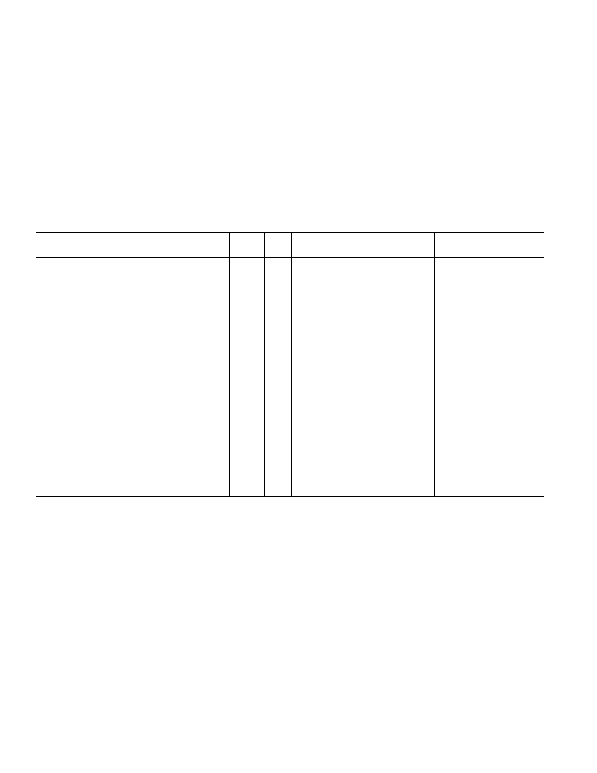
AD9617–SPECIFICATIONS
ABSOLUTE MAXIMUM RATINGS
Supply Voltages (±V
) . . . . . . . . . . . . . . . . . . . . . . . . . . . +7 V
S
1
Common-Mode Input Voltage . . . . . . . . . . . . . . . . . . . . . ±Vs
Differential Input Voltage . . . . . . . . . . . . . . . . . . . . . . . . . 3 V
Continuous Output Current
2
. . . . . . . . . . . . . . . . . . . . . 70 mA
Operating Temperature Ranges
AD9617JN/JR . . . . . . . . . . . . . . . . . . . . . . . . 0°C to +70°C
Storage Temperature
AD9617JN/JR . . . . . . . . . . . . . . . . . . . . . –65°C to +125°C
Junction Temperature
3
NOTES
1
Absolute maximum ratings are limiting values to be applied individually and
beyond which the serviceability of the circuit may be impaired. Functional
operability is not necessarily implied. Exposure to absolute maximum rating
conditions for an extended period of time may affect device reliability.
2
Output is short circuit protected to ground, but not to supplies. Continuous
short circuit to ground may affect device reliability.
3
Typical thermal impedances (part soldered onto board):
Plastic DIP: θ
θ
= 40°C/W.
JC
= 140°C/W; θJC = 30°C/W. SOIC Package: θJA = 155°C/W;
JA
AD9617JN/JR . . . . . . . . . . . . . . . . . . . . . . . . . . . . . +150°C
Lead Soldering Temperature (10 Seconds) . . . . . . . . . +300°C
DC ELECTRICAL CHARACTERISTICS
Parameter Conditions Temp Level Min Typ Max Min Typ Max Min Typ Max Units
Input Offset Voltage
Input Offset Voltage TC
Input Bias Current
Inverting +25°C I –50 0 +50 –50 0 +50 –25 0 +25 µA
Noninverting +25°C I –25 +5 +35 –25 +5 +35 –15 +5 +20 µA
Input Bias Current TC
Noninverting Full IV –50 +30 +125 –50 +30 +125 –50 +30 +125 nA/°C
Inverting Full IV –50 +50 +150 –50 +50 +150 –50 +50 +150 nA/°C
Input Resistance
Noninverting +25°C V 60 60 60 kΩ
Input Capacitance
Noninverting +25°C V 1.5 1.5 1.5 pF
Common-Mode Input Range
Common-Mode Rejection Ratio
Power Supply Rejection Ratio ∆V
Open Loop Gain
T
O
Nonlinearity At DC +25°C IV 10 10 10 ppm
Output Voltage Range +25°CII ±3.4 ± 3.8 ±3.4 ± 3.8 ±3.4 +3.8 V
Output Impedance At DC +25°C V 0.07 0.07 0.07 Ω
Output Current (50 Ω Load) T = +25°C to T
NOTES
*Pending obsoletion: last-time buy October 25, 1999.
1
Measured with respect to the inverting input.
2
Typical is defined as the mean of the distribution.
3
Measured in voltage follower configuration.
4
Measured with VIN = +0.25 V.
Specifications subject to change without notice.
1, 2
2
2
2
3
T = T
MAX
4
T = T
T = T
T = T
to +25°C ← II ±1.7 ±1.8 ±1.7 ±1.8 ±1.7 ±1.8 V
MIN
to T
MIN
MAX
to +25°C ← II 48 51 48 51 48 51 dB
MIN
= ±5% Full II 48 51 48 51 48 51 dB
S
At DC +25°C V 500 500 500 kΩ
T = T
MIN
(Unless otherwise noted, AV = +3; 6VS = 65 V; RF = 400 V; R
= 100 V)
LOAD
Test AD9617JN/JR AD9617AQ/SQ* AD9617BQ/TQ*
+25°C I –1.1 +0.5 +2.2 –1.1 +0.5 +2.2 +0.0 +0.5 +1.35 mV
Full IV –4 +3 +25 –4 +3 +25 –4 +3 +25 µV/°C
← II ±1.4 ±1.5 ±1.4 ±1.5 ±1.4 ±1.5 V
← II 44 48 44 48 44 48 dB
← II 60 60 60 mA
MAX
← II 50 50 50 mA
–2–
REV. B
Page 3
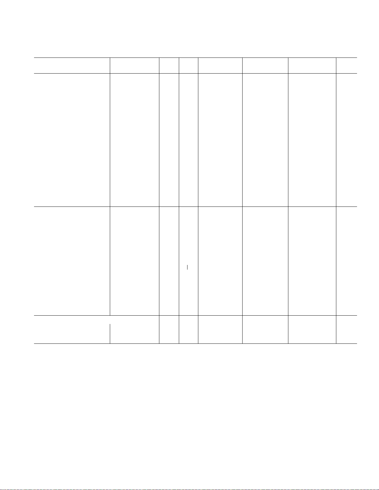
AD9617
AC ELECTRICAL CHARACTERISTICS
(Unless otherwise noted, AV = +3; 6VS = 65 V; RF = 400 V; R
= 100 V)
LOAD
Test AD9617JN/JR AD9617AQ/SQ* AD9617BQ/TQ*
Parameter Conditions Temp Level Min Typ Max Min Typ Max Min Typ Max Units
FREQUENCY DOMAIN
Bandwidth (–3 dB)
Small Signal V
Large Signal V
Bandwidth Variation vs. A
V
Amplitude of Peaking (<50 MHz) T = T
Amplitude of Peaking (>50 MHz) T = T
≤ 2 V p-p Full II 135 190 145 190 145 190 MHz
OUT
= 4 V p-p Full IV 150 115 150 115 150 MHz
OUT
A
= –1 to ±15 +25°C V 40 40 40 MHz
V
to +25°C ← II 0 0 0.3 0 0.3 dB
T = T
T = T
MIN
MAX
to +25°C ← II 0 0 0.8 0 0.8 dB
MIN
MAX
← II 0 0 0.6 0 0.6 dB
← II 0 0 1.0 0 1.0 dB
Amplitude of Roll-Off (<60 MHz) Full II 0.1 0.1 0.6 0.1 0.6 dB
Phase Nonlinearity DC to 75 MHz +25°C V 0.5 0.5 0.5 Degree
2nd Harmonic Distortion 2 V p-p; 4.3 MHz Full IV –86 –78 –86 –78 –86 –78 dBc
2 V p-p; 20 MHz Full IV –67 –59 –67 –59 –67 –59 dBc
2 V p-p; 60 MHz Full II –51 –43 –51 –43 –51 –43 dBc
3rd Harmonic Distortion 2 V p-p; 4.3 MHz Full IV –83 –75 –83 –75 –83 –75 dBc
2 V p-p; 20 MHz Full IV –69 –61 –69 –61 –69 –61 dBc
2 V p-p; 60 MHz Full II –54 –46 –54 –46 –54 –46 dBc
Input Noise Voltage 10 MHz +25°C V 1.2 1.2 1.2 nV/√Hz
Inverting Input Noise Current 10 MHz +25°C V 29 29 29 pA/√Hz
Average Equivalent Integrated
Input Noise Voltage 0.1 MHz to 200 MHz +25°C V 55 55 55 µV, rms
TIME DOMAIN
Slew Rate V
= 4 V Step Full IV 1400 1100 1400 1100 1400 V/µs
OUT
Rise/Fall Time
= 2 V Step Full IV 2.0 2.0 2.5 2.0 2.5 ns
V
OUT
= 4 V Step T = +25°C to T
V
OUT
V
= 4 V Step T = T
OUT
Overshoot V
MIN
= 2 V Step Full IV 3 3 14 3 14 %
OUT
← IV 2.4 2.4 3.3 2.4 3.3 ns
MAX
← IV 2.4 2.4 3.5 2.4 3.5 ns
Settling Time
To 0.1% V
To 0.02% V
To 0.1% V
To 0.02% V
= 2 V Step Full IV 10 10 15 10 15 ns
OUT
= 2 V Step Full IV 14 14 23 14 23 ns
OUT
= 4 V Step Full IV 11 11 16 11 16 ns
OUT
= 4 V Step Full IV 16 16 24 16 24 ns
OUT
2× Overdrive Recovery to
±2 mV of Final Value V
Propagation Delay +25°CV 2 2 2 ns
Differential Gain
Differential Phase
1
1
= 1.7 V Step +25°C V 50 50 50 ns
IN
Full V <0. 01 <0. 01 <0 .01 %
Full V 0.01 0.01 0.01 Degree
POWER SUPPLY REQUIREMENTS
Quiescent Current
+I
S
–I
S
NOTES
*Pending obsoletion: last-time buy October 25, 1999.
1
Frequency = 4.3 MHz; R
Specifications subject to change without notice.
= 150 Ω; A
L
= +3.
V
Full II 34 48 34 48 34 48 mA
Full II 34 48 34 48 34 48 mA
REV. B
–3–
Page 4

AD9617
EXPLANATION OF TEST LEVELS
Test Level
I - 100% production tested.
II - 100% production tested at +25°C and sample tested at
specified temperatures. AC testing of J grade devices done
on sample basis.
III - Sample tested only.
IV - Parameter is guaranteed by design and characterization
testing.
V - Parameter is a typical value only.
VI - All devices are 100% production tested at +25°C. 100%
production tested at temperature extremes for extended
temperature devices; sample tested at temperature ex-
tremes for commercial/industrial devices.
ORDERING GUIDE
Temperature Package Package
Model Range Description Option
AD9617JN 0°C to +70°C Plastic DIP N-8
AD9617JR 0°C to +70°C SOIC SO-8
AD9617JR-REEL 0°C to +70°C 13" Tape and Reel SO-8
–INPUT
+INPUT
DIE CONNECTIONS
+V
S
TOP VIEW
(Not to Scale)
–V
DIE SIZE = 53 3 67 3 15 mils
–V
S
S
+V
S
OUTPUT
–4–
REV. B
Page 5

AD9617
g
g
FREQUENCY – Hz
10
100
dB
1k 10k 100k 1M 100M
15
20
25
30
35
40
45
50
55
60
CMRR
PSRR
10M
TIME – ms
0.1
0
SETTLING PERCENTAGE – %
816243240
0.08
0.06
0.04
0.02
0
–0.02
–0.04
–0.1
V
OUT
= 4V STEP
100V
TEST CIRCUIT
6pF
–0.06
–0.08
TIME – ms
0.1
0
SETTLING PERCENTAGE – %
246810
0.08
0.06
0.04
0.02
0
–0.02
–0.04
–0.1
V
OUT
= 4V STEP
100V
TEST CIRCUIT
6pF
–0.06
–0.08
Typical Performance Characteristics
3
2
1
0
–1
–2
–3
MAGNITUDE – dB
–4
–5
–6
–7
0
40 80 120 160 200
= +5
A
V
= +20
A
V
FREQUENCY – MHz
Figure 1. Noninverting Frequency Response
3
MAGNITUDE – dB
2
1
0
–1
–2
–3
–4
–5
–6
–7
0
40 80 120 160 200
AV = –5
A
= –20
V
FREQUENCY – MHz
Figure 2. Inverting Frequency Response
A
A
V
V
= +1
= –1
180
135
90
45
0
–45
–90
–135
–180
180
135
90
45
0
–45
–90
–135
–180
(AV = +3; 6VS = 65 V; RF = 400 V, unless otherwise noted)
PHASE – Degrees
Figure 4. CMRR and PSRR
rees
PHASE – De
Figure 5. Settling Time
120
105
90
75
60
GAIN – dB
45
30
15
REV. B
GAIN
PHASE
TEST CIRCUIT
FREQUENCY – Hz
100V
0
10k
100k 1M 10M 100M 1G
Figure 3. Open Loop Transimpedance Gain
[
T(s) Relative to 1
Ω]
0
30
60
rees
90
120
150
180
RELATIVE PHASE – De
210
240
–5–
Figure 6. Long Term Settling Time
Page 6

AD9617
g
–dBc
100
MAGNITUDE – dB
40
V
= 2V p-p
OUT
50
60
70
80
90
= 2ND HARMONIC
= 3RD HARMONIC
100V LOAD
0
24610
8
FREQUENCY – MHz
20 40 60 100
Figure 7. Harmonic Distortion
3
2
1
0
–1
–2
–3
–4
–5
–6
–7
0
40 80 120 160 200
RL = 100V
= 50V
R
L
FREQUENCY – MHz
Figure 8. Frequency Response vs. R
500V LOAD
= 500V
R
L
LOAD
180
135
90
45
0
–45
–90
–135
–180
rees
PHASE – De
INTERCEPT – +dBm
ANALOG INPUT – Volts
50
50V
40
30
20
0
30 60 90 120 150
FREQUENCY – MHz
TEST
CIRCUIT
50V
Figure 10. Intermodulation Distortion (IMD)
2.5
2.0
1.5
1.0
0.5
0
–0.5
–1.0
–1.5
–2.0
–2.5
= +3
A
V
TEST CIRCUIT
100V
A
= –3
V
10ns/DIV
6pF
Figure 11. Large Signal Pulse Response
115
100
85
70
pA/ Hz
55
40
25
100
pA/ Hz
(INVERTING)
nV/ Hz
1k 10k 100k
FREQUENCY – MHz
Figure 9. Equivalent Input Noise
7
6
5
4
3
2
1
nV/ Hz
–6–
= +3
A
V
1.0
0.5
0
–0.5
–1.0
ANALOG INPUT – Volts
TEST CIRCUIT
100V
A
= –3
V
10ns/DIV
6pF
Figure 12. Small Signal Pulse Response
REV. B
Page 7

AD9617
V
OUT
– Volts
–2
ERROR RELATIVE TO FS
0.0002%/DIVISION
0%
–1
0
12
R
L
= 100V
THEORY OF OPERATION
The AD9617 has been designed to combine the key attributes of
traditional “low frequency” precision amplifiers with exceptional
high frequency characteristics that are independent of closedloop gain. Previous “high frequency” closed-loop amplifiers have
low open loop gain relative to precision amplifiers. This results
in relatively poor dc nonlinearity and precision, as well as excessive high frequency distortion due to open loop gain roll-off.
Operational amplifiers use two basic types of feedback correction, each with advantages and disadvantages. Voltage feedback
topologies exhibit an essentially constant gain bandwidth product. This forces the closed-loop bandwidth to vary inversely with
closed-loop gain. Moreover, this type design typically slew rate
limits in a way that causes the large signal bandwidth to be
much lower than its small signal characteristics.
A newer approach is to use current feedback to realize better
dynamic performance. This architecture provides two key attributes over voltage feedback configurations: (1) avoids slew
rate limiting and therefore large signal bandwidth can approach
small signal performance; and (2) low bandwidth variation versus gain settings, due to the inherently low open loop inverting
input resistance (R
).
S
The AD9617 uses a new current feedback topology that overcomes these limitations and combines the positive attributes of
both current feedback and voltage feedback designs. These
devices achieve excellent high frequency dynamics (slew, BW
and distortion) along with excellent low frequency linearity and
good dc precision.
DC GAIN CHARACTERISTICS
A simplified equivalent schematic is shown below. When operating the device in the inverting mode, the input signal error
current (I
(T
O
feedback is applied through R
gain (G) equal to –R
) is amplified by the open loop transimpedance gain
E
). The output signal generated is equal to TO × IE. Negative
such that the device operates at a
F
.
F/RI
Noninverting operation is similar, with the input signal applied
to the high impedance buffer (noninverting) input. As before, an
output (buffer) error current (I
) is generated at the low imped-
E
ance inverting input. The signal generated at the output is fed
back to the inverting input such that the external gain is (l + R
R
). The feedback mechanics are identical to the voltage feed-
I
/
F
back topology when exact equations are used.
The major difference lies in the front end architecture. A voltage
feedback amplifier has symmetrical high resistance (buffered)
inputs. A current feedback amplifier has a high noninverting
resistance (buffered) input and a low inverting (buffer output)
input resistance. The feedback mechanics can be easily developed using current feedback and transresistance open loop gain
T(s) to describe the I/O relationship. (See typical specification
chart.)
DC closed-loop gain for the AD9617 can be calculated using
the following equations:
G =
G =
where
V
O
V
I
V
O
V
N
1
LG
/ R
−R
F
≈
1 +1/ LG
1 + R
≈
≈
I
/ R
F
I
1 +1/ LG
R
+ R
()
SRF
Ts
()
i R
S
I
RSiR
()
I
inverting (1)
noninverting (2)
(3)
Because the noninverting input buffer is not ideal, input resistance R
noninverting operation than for inverting operation. R
(at dc) is gain dependent and is typically higher for
S
will
S
approach the same value (<7 Ω) for both at input frequencies
above 50 MHz. Below the open loop corner frequency, the
noninverting R
RSnoninverting
where: A
Inverting R
can be approximated as:
S
Ts
()
()
= Open Loop Voltage Gain < G × 600
O
below the open loop corner frequency can be ap-
S
≈7+
A
O
=7+
T
A
O
O
dc
(4)
proximated as:
Ts
()
A
O
where: A
RSinverting
()
= 40,000.
O
≈7+
The AD9617 approaches this condition. With T
R
= 500 Ω and RS = 25 Ω (dc), a gain error no greater than
L
=7+
T
A
O
O
dc
= 1 × 10
O
(5)
6
Ω,
0.05% typically results for G = –1 and 0.15% for G = –40.
Moreover, the architecture linearizes the open loop gain over its
operating voltage range and temperature resulting in ≥16 bits of
linearity.
REV. B
+
V
N
L
S
R
R
I
V
C
I
I
S
I
E
–
C
C
T
O
R
F
V
O
Figure 13. Equivalent Circuit
Figure 14. DC Nonlinearity vs. V
OUT
–7–
Page 8

AD9617
AC GAIN CHARACTERISTICS
Closed-loop bandwidth at high frequencies is determined primarily by the roll-off of T(s). But circuit layout is critical to
minimize external parasitics which can degrade performance by
causing premature peaking and/or reduced bandwidth.
The inverting and noninverting dynamic characteristics are similar.
When driving the noninverting input, the inverting input capacitance (C
) will cause the noninverting closed-loop bandwidth to
I
be higher than the inverting bandwidth for gains less than two
(2). In the remaining cases, inverting and noninverting responses
are nearly identical.
For best overall dynamic performance, the value of the feedback
resistor (R
) should be 400 ohms. Although bandwidth reduces
F
as closed-loop gain increases, the change is relatively small due
to low equivalent series input impedance, Z
. (See typical
S
performance charts.) The simplified equations governing the
device’s dynamic performance are shown below.
Closed-Loop Gain vs. Frequency:
(noninverting operation)
R
F
V
V
where: t = R
Slew Rate ≈
where:
1+
≈
R
I
R
S
st 1+
R
I
× CC = 0.9 ns (R
F
∆V
RFKC
K =1 +
+ 1
= 400 Ω)
F
O
−τ/R
FKCC
× e
C
R
S
R
I
(6)
(7)
O
I
Increasing Bandwidth at Low Gains
By reducing RF, wider bandwidth and faster pulse response can
be attained beyond the specified values, although increased
overshoot, settling time and possible ac peaking may result. As a
rule of thumb, overshoot and bandwidth will increase by 1%
and 8%, respectively, for a 5% reduction in R
at gains of ±10.
F
Lower gains will increase these sensitivities.
Equations 6 and 7 are simplified and do not accurately model
the second order (open loop) frequency response term which is
the primary contributor to overshoot, peaking and nonlinear
bandwidth expansion. (See Open Loop Bode Plots.) The user
should exercise caution when selecting R
values much lower
F
than 400 Ω. Note that a feedback resistor must be used in all
situations, including those in which the amplifier is used in a
noninverting unity gain configuration.
Increasing Bandwidth at High Gains
Closed loop bandwidth can be extended at high closed loop gain
by reducing R
current being split between R
a given R
Bandwidth reduction is a result of the feedback
F.
), more feedback current is shunted through RI, which
F
and RI. As the gain increases (for
S
reduces closed loop bandwidth (see Equation 6). To maintain
specified BW, the following equations can be used to approximate R
and R
F
= 424 ± 8 G (8)
R
F
for any gain from ±l to ±15.
I
(+ for inverting and – for noninverting)
424 −8 G
R
R
≈
I
424 +8 G
≈
I
G −1
G −1
(noninverting) (9)
(inverting) (10)
G = Closed Loop Gain.
Bandwidth Reduction
The closed loop bandwidth can be reduced by increasing R
F.
Equations 6 and 7 can be used to determine the closed loop
bandwidth for any value R
tor across R
, as this will degrade dynamic performance and
F
. Do not connect a feedback capaci-
F
possibly induce oscillation.
DC Precision and Noise
Output offset voltage results from both input bias currents and
input offset voltage. These input errors are multiplied by the
noise gain term (1 + R
) and algebraically summed at the
F/RI
output as shown below.
V
O=VIO
× 1 +
R
F
R
I
± IBn × R
N
× 1 +
R
F
R
I
± IBi × R
F
(11)
Since the inputs are asymmetrical, IBi and IBn do not correlate.
Canceling their output effects by making R
= RFiRI will not
N
reduce output offset errors, as it would for voltage feedback
amplifiers. Typically, IBn is 5 µA and V
is +0.5 mV (I sigma =
IO
0.3 mV), which means that the dc output error can be reduced
by making R
≈ 100 Ω. Note that the offset drift will not change
N
significantly because the IBn TC is relatively small. (See specification table.)
R
F
IBi
R
I
IBn
R
N
V
OUT
Figure 15. Output Offset Voltage
IBi/IBn – mA
–10
10
5
0
–5
–558C
IBn
V
IO
IBi
258C 1258C
1.0
0.5
0
–0.5
–1.0
– mA
IO
V
Figure 16. DC Accuracy
–8–
REV. B
Page 9

AD9617
S
The effective noise at the output of the amplifier can be determined by taking the root sum of the squares of Equation 11 and
applying the spectral noise values found in the typical graph
section. This applies to noise from the op amp only. Note that
both the noise figure and equivalent input offset voltages improve as the closed loop gain is increased (by keeping R
and reducing R
with R
I
CLI
In
= 0 Ω).
N
400V
R
SERIES
500V
R
L
CL
fixed
F
Figure 17. Capacitive Load Figure
Capacitive Load Considerations
Due to the low inverting input resistance (RS) and output buffer
design, the AD9617 can directly handle input and/or output
load capacitances of up to 20 pF. See the chart below.
A small series resistor can be used at the output of the amplifier
and outside of the feedback loop to facilitate driving larger capacitive loads or for obtaining faster settling time. For capacitive
loads above 20 pF, R
35
V
= 4V STEP
OUT
CL = 0pF
30
25
20
15
SETTLING TIME TO 0.02% – ns
10
5pF 4pF/DIV 25pF
INPUT CAPACITANCE – CLI
should be considered.
SERIES
V
CLI = 0pF
10pF 4pF/DIV 30pF
= 0V
R
SERIES
= 4V STEP
OUT
INPUT CAPACITANCE – CL
Figure 18. Input/Output Capacitance Comparisons
25
APPLYING THE AD9617
The superior frequency and time domain specifications of the
AD9617 make it an obvious choice for driving flash converters
and buffering the outputs of high speed DACs. Its outstanding
distortion and noise performance make it well suited as a driver
for analog to digital converters (ADCs) with resolutions as high
as 16 bits.
Typical circuits for inverting and noninverting applications are
shown in Figures 20 and 21.
Closed-loop gain for noninverting configurations is determined
by the value of RI according to the equation:
R
G =1 +
F
R
I
+V
S
3.3mF
0.1mF
0.1mF
V
IN
R
IN
AD9617
400V
R
I
0.1mF
0.1mF
3.3mF
–V
V
OUT
(12)
Figure 20. Noninverting Operation
+V
S
3.3mF
0.1mF
0.1mF
REV. B
20
15
– V
SERIES
10
R
5
0
0
20 40 60 80 100
CL – pF
Figure 19. Recommended R
SERIES
vs. CL
–9–
AD9617
R
R
I
TERM
V
IN
400V
0.1mF
0.1mF
3.3mF
–V
S
Figure 21. Inverting Operation
V
OUT
Page 10

AD9617
LAYOUT CONSIDERATIONS
As with all high performance amplifiers, printed circuit layout is
critical in obtaining optimum results with the AD9617. The
ground plane in the area of the amplifier should cover as much
of the component side of the board as possible. Each power
supply trace should be decoupled close to the package with at
least a 3.3 µF tantalum and a low inductance, 0.1 µF ceramic
capacitor.
OUTLINE DIMENSIONS
Dimensions shown in inches and (mm).
Small Outline Package
(SO-8)
0.1 98 (5.00)
0.1 88 (4.74)
0.158 (4.00)
0.150 (3.80)
PIN 1
0.010 (0.25)
0.004 (0.10)
SEATING
85
0.050 (1.27)
PLANE
41
BSC
0.018 (0.46)
0.014 (0.36)
0.244 (6.200)
0.228 (5.80)
0.069 (1.75)
0.053 (1.35)
All lead lengths for input, output and the feedback resistor
should be kept as short as possible. All gain setting resistors
should be chosen for low values of parasitic capacitance and
inductance, i.e., microwave resistors and/or carbon resistors.
Stripline techniques should be used for lead lengths in excess of
one inch. Sockets should be avoided if possible because of their
stray inductance and capacitance.
0.205 (5.20)
0.181 (4.60)
88
08
0.015 (0.38)
0.007 (0.18)
0.045 (1.15)
0.020 (0.50)
C1353b–0–9/99
PIN 1
0.210
(5.33)
MAX
0.200 (5.05)
0.125 (3.18)
0.022 (0.558)
0.014 (0.356)
Plastic DIP
0.430 (10.92)
0.348 (8.84)
8
0.100 (2.54)
5
0.280 (7.11)
14
BSC
0.240 (6.10)
0.070 (1.77)
0.045 (1.15)
(N-8)
0.060 (1.52)
0.015 (0.38)
0.150
(3.81)
MIN
SEATING
PLANE
0.325 (8.25)
0.300 (7.62)
08–158
0.015 (0.381)
0.008 (0.204)
PRINTED IN U.S.A.
–10–
REV. B
 Loading...