

Page 1
Clock Generator with Dual PLLs,
Data Sheet
FEATURES
Fully integrated dual PLL/VCO cores
1 integer-N and 1 fractional-N PLL
Continuous frequency coverage from 11.2 MHz to 200 MHz
Most frequencies from 200 MHz to 637.5 MHz available
PLL1 phase jitter (12 kHz to 20 MHz): 460 fs rms typical
PLL2 phase jitter (12 kHz to 20 MHz)
Integer-N mode: 470 fs rms typical
Fractional-N mode: 660 fs rms typical
Input crystal or reference clock frequency
Optional reference frequency divide-by-2
2
I
C programmable output frequencies
Up to 4 LVDS/LVPECL or up to 8 LVCMOS output clocks
1 CMOS buffered reference clock output
Spread spectrum: downspread [0, −0.5]%
2 pin-controlled frequency maps: margining
Integrated loop filters
Space saving, 6 mm × 6 mm, 40-lead LFCSP package
1.02 W power dissipation (LVDS operation)
1.235 W power dissipation (LVPECL operation)
3.3 V operation
APPLICATIONS
Low jitter, low phase noise multioutput clock generator for
data communications applications including Ethernet,
Fibre Channel, SONET, SDH, PCI-e, SATA, PTN, OTN,
ADC/DAC, and digital video
Spread spectrum clocking
GENERAL DESCRIPTION
The AD9577 provides a multioutput clock generator function,
along with two on-chip phase-locked loop cores, PLL1 and PLL2,
optimized for network clocking applications. The PLL designs
are based on the Analog Devices, Inc., proven portfolio of high
performance, low jitter frequency synthesizers to maximize
network performance. The PLLs have I
frequencies and formats. The fractional-N PLL can support
spread spectrum clocking for reduced EMI radiated peak power.
Both PLLs can support frequency margining. Other applications
with demanding phase noise and jitter requirements can benefit
from this part.
The first integer-N PLL section (PLL1) consists of a low noise phase
frequency detector (PFD), a precision charge pump (CP), a low
phase noise voltage controlled oscillator (VCO), a programmable
Rev. 0
Information furnished by Analog Devices is believed to be accurate and reliable. However, no
responsibility is assumed by Anal og Devices for its use, nor for any infringements of patents or ot her
rights of third parties that may result from its use. Specifications subject to change without notice. No
license is granted by implication or otherwise under any patent or patent rights of Analog Devices.
Trademarks and registered trademarks are the property of their respective owners.
2
C programmable output
Spread Spectrum, and Margining
AD9577
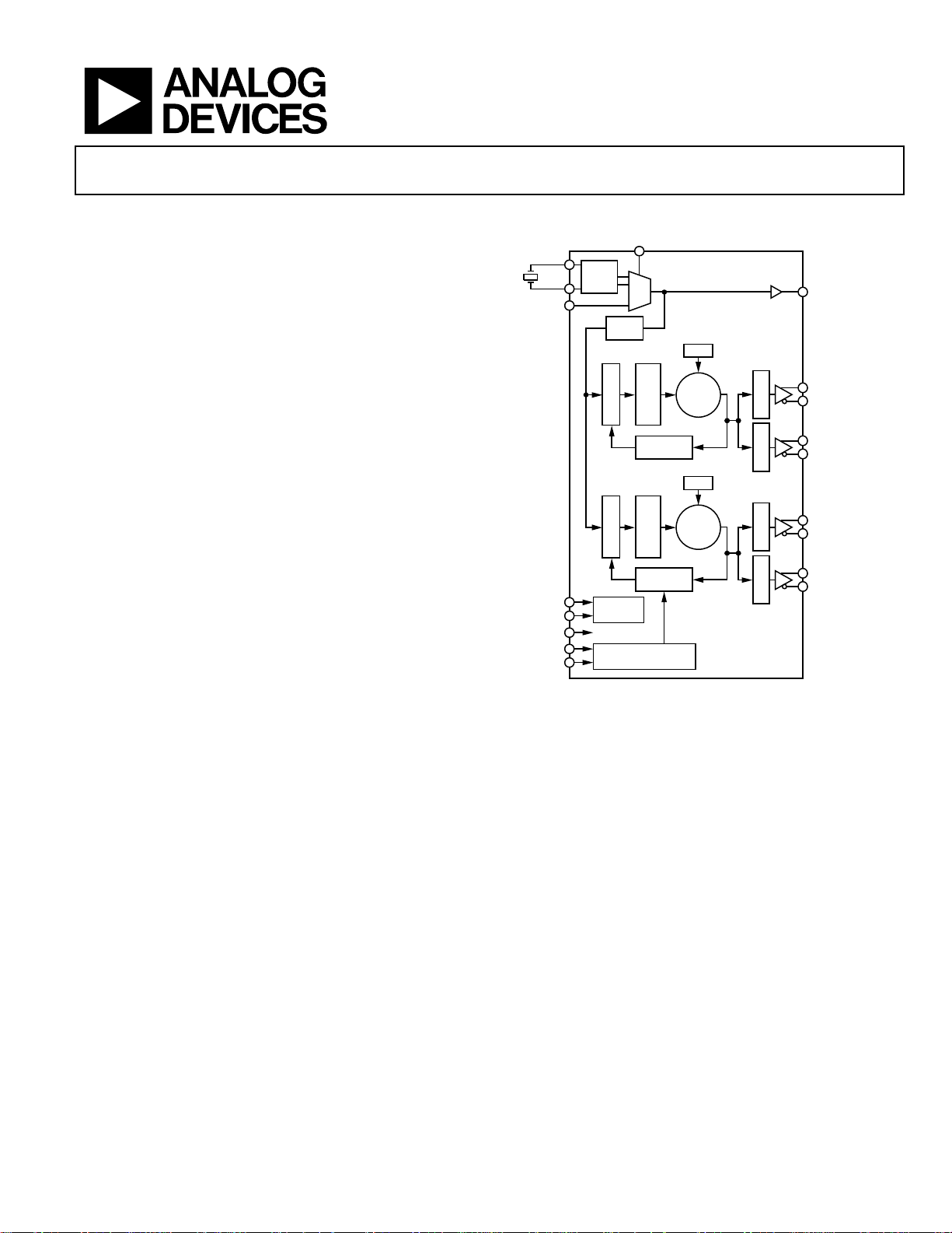
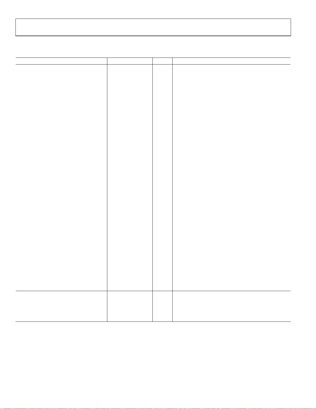
FUNCTIONAL BLOCK DIAGRAM
REFSEL
XT1
XTAL
OSC
XT2
REFCLK
DIVIDE
1 OR 2
THIRD
ORDER LPF
DIVIDER
THIRD
ORDER LPF
DIVIDER
LDO
VCO
2.15GHz
TO
2.55GHz
LDO
VCO
2.15GHz
TO
2.55GHz
Figure 1.
SCL
SDA
MARGIN
SSCG
MAX_BW
PLL1
PFD
f
PFD/CP
FEEDBACK
PLL2
PFD/CP
FEEDBACK
I2C
CONTROL
SPREAD SPECTRUM,
SDM
feedback divider, and two independently programmable output
dividers. By connecting an external crystal or applying a reference
clock to the REFCLK pin, frequencies of up to 637.5 MHz can
be synchronized to the input reference. Each output divider and
feedback divider ratio is I
2
C programmed for the required
output rates.
A second fractional-N PLL (PLL2) with a programmable modulus
allows VCO frequencies that are fractional multiples of the
reference frequency to be synthesized. Each output divider
and feedback divider ratio can be programmed for the required
output rates, up to 637.5 MHz. This fractional-N PLL can also
operate in integer-N mode for the lowest jitter.
Up to four differential output clock signals can be configured
as either LVPECL or LVDS signaling formats. Alternatively,
the outputs can be configured for up to eight CMOS outputs.
Combinations of these formats are supported. No external loop
filter components are required, thus conserving valuable design
time and board space. The AD9577 is available in a 40-lead, 6 mm ×
6 mm LFCSP package and can operate from a single 3.3 V supply.
The operating temperature range is −40°C to +85°C.
One Technology Way, P.O. Box 9106, Norwood, MA 02062-9106, U.S.A.
Tel: 781.329.4700 www.analog.com
Fax: 781.461.3113 ©2011 Analog Devices, Inc. All rights reserved.
CMOS
DIVIDERS
DIVIDERS
DIVIDERS
DIVIDERS
AD9577
REFOUT
LVPECL/LVDS
OR 2 × CMOS
LVPECL/LVDS
OR 2 × CMOS
LVPECL/LVDS
OR 2 × CMOS
LVPECL/LVDS
OR 2 × CMOS
09284-001
Page 2

AD9577 Data Sheet
TABLE OF CONTENTS
Features.............................................................................................. 1
Applications....................................................................................... 1
General Description ......................................................................... 1
Functional Block Diagram .............................................................. 1
Revision History ............................................................................... 2
Specifications..................................................................................... 3
PLL1 Characteristics .................................................................... 3
PLL1 Clock Output Jitter............................................................. 5
PLL2 Fractional-N Mode Characteristics ................................. 6
PLL2 Integer-N Mode Characteristics....................................... 7
PLL2 Clock Output Jitter............................................................. 9
CMOS Reference Clock Output Jitter...................................... 11
Timing Characteristics .............................................................. 12
Clock Outputs............................................................................. 13
Power............................................................................................ 14
Crystal Oscillator........................................................................ 15
Reference Input........................................................................... 15
Control Pins ................................................................................ 15
Absolute Maximum Ratings.......................................................... 16
Thermal Characteristics ............................................................16
ESD Caution................................................................................ 16
Pin Configuration and Function Descriptions........................... 17
Typical Performance Characteristics ........................................... 19
REFOUT and PLL1 Phase Noise Performance...................... 19
PLL2 Phase Noise Performance................................................ 20
Output Jitter ................................................................................21
Typical Output Signal ................................................................ 22
Typical Spread Spectrum Performance Characteristics........ 24
Terminology .................................................................................... 25
Detailed Block Diagram ................................................................ 27
Example Application.................................................................. 28
Functional Description.................................................................. 29
Reference Input and Reference Dividers................................. 29
Output Channel Dividers.......................................................... 30
Outputs........................................................................................ 30
Reference Output Buffer ........................................................... 31
PLL1 Integer-N PLL................................................................... 31
PLL1 Phase Frequency Detector (PFD) and Charge Pump . 32
PLL1 VCO................................................................................... 32
PLL1 Feedback Divider ............................................................. 32
Setting the Output Frequency of PLL1.................................... 32
PLL2 Integer/Fractional-N PLL ............................................... 32
PLL2 Phase Frequency Detector (PFD) and Charge Pump . 33
PLL2 Loop Bandwidth............................................................... 33
PLL2 VCO................................................................................... 33
PLL2 Feedback Divider ............................................................. 33
PLL2 Σ-Δ Modulator ................................................................. 33
Spur Mechanisms....................................................................... 33
Optimizing PLL Performance .................................................. 34
Setting the Output Frequency of PLL2.................................... 34
Margining.................................................................................... 35
Spread Spectrum Clock Generation (SSCG).......................... 35
I2C Interface Timing and Internal Register Description........... 38
Default Frequency Map and Output Formats ........................ 40
I2C Interface Operation ............................................................. 40
Typical Application Circuits ..................................................... 42
Power and Grounding Considerations and Power Supply
Rejection...................................................................................... 43
Outline Dimensions....................................................................... 44
Ordering Guide .......................................................................... 44
REVISION HISTORY
10/11—Revision 0: Initial Version
Rev. 0 | Page 2 of 44
Page 3
Data Sheet AD9577
SPECIFICATIONS
Typical (typ) is given for VS = 3.3 V, TA = 25°C, unless otherwise noted. Minimum (min) and maximum (max) values are given over full
(3.0 V to 3.6 V) and TA (−40°C to +85°C) variation. AC coupling capacitors of 0.1 μF used where appropriate. A Fox Electronics
V
S
FX532A 25 MHz crystal is used throughout, unless otherwise stated.
PLL1 CHARACTERISTICS
Table 1.
Parameter Min Typ Max Unit Test Conditions/Comments1
NOISE CHARACTERISTICS
Phase Noise (106.25 MHz LVPECL Output) Na = 102, Vx = 4, Dx = 6, f
At 1 kHz −121 dBc/Hz
At 10 kHz −127 dBc/Hz
At 100 kHz −128 dBc/Hz
At 1 MHz −150 dBc/Hz
At 10 MHz −156 dBc/Hz
At 30 MHz −158 dBc/Hz
Phase Noise (156.25 MHz LVPECL Output) Na = 100, Vx = 4, Dx = 4, f
At 1 kHz −117 dBc/Hz
At 10 kHz −124 dBc/Hz
At 100 kHz −124 dBc/Hz
At 1 MHz −147 dBc/Hz
At 10 MHz −156 dBc/Hz
At 30 MHz −156 dBc/Hz
Phase Noise (625 MHz LVPECL Output) Na = 100, Vx = 2, Dx = 2, f
At 1 kHz −105 dBc/Hz
At 10 kHz −112 dBc/Hz
At 100 kHz −112 dBc/Hz
At 1 MHz −135 dBc/Hz
At 10 MHz −150 dBc/Hz
At 30 MHz −150 dBc/Hz
Phase Noise (106.25 MHz LVDS Output) Na = 102, Vx = 4, Dx = 6, f
At 1 kHz −119 dBc/Hz
At 10 kHz −127 dBc/Hz
At 100 kHz −128 dBc/Hz
At 1 MHz −148 dBc/Hz
At 10 MHz −156 dBc/Hz
At 30 MHz −156 dBc/Hz
Phase Noise (156.25 MHz LVDS Output) Na = 100, Vx = 4, Dx = 4, f
At 1 kHz −116 dBc/Hz
At 10 kHz −124 dBc/Hz
At 100 kHz −124 dBc/Hz
At 1 MHz −145 dBc/Hz
At 10 MHz −155 dBc/Hz
At 30 MHz −155 dBc/Hz
Phase Noise (625 MHz LVDS Output) Na = 100, Vx = 2, Dx = 2, f
At 1 kHz −104 dBc/Hz
At 10 kHz −111 dBc/Hz
At 100 kHz −112 dBc/Hz
At 1 MHz −134 dBc/Hz
At 10 MHz −149 dBc/Hz
At 30 MHz −149 dBc/Hz
= 25 MHz
PFD
= 25 MHz
PFD
= 25 MHz
PFD
= 25 MHz
PFD
= 25 MHz
PFD
= 25 MHz
PFD
Rev. 0 | Page 3 of 44
Page 4
AD9577 Data Sheet
Parameter Min Typ Max Unit Test Conditions/Comments1
Phase Noise (106.25 MHz CMOS Output) Na = 102, Vx = 4, Dx = 6, f
At 1 kHz −118 dBc/Hz
At 10 kHz −127 dBc/Hz
At 100 kHz −127 dBc/Hz
At 1 MHz −149 dBc/Hz
At 10 MHz −156 dBc/Hz
At 30 MHz −157 dBc/Hz
Phase Noise (156.25 MHz CMOS Output) Na = 100, Vx = 4, Dx = 4, f
At 1 kHz −115 dBc/Hz
At 10 kHz −124 dBc/Hz
At 100 kHz −124 dBc/Hz
At 1 MHz −146 dBc/Hz
At 10 MHz −155 dBc/Hz
At 30 MHz −155 dBc/Hz
Phase Noise (155.52 MHz LVPECL Output) Na = 112, Vx = 2, Dx = 7, f
At 1 kHz −117 dBc/Hz
At 10 kHz −122 dBc/Hz
At 100 kHz −123 dBc/Hz
At 1 MHz −148 dBc/Hz
At 10 MHz −156 dBc/Hz
At 30 MHz −156 dBc/Hz
Phase Noise (622.08 MHz LVPECL Output) Na = 128, Vx = 2, Dx = 2, f
At 1 kHz −105 dBc/Hz
At 10 kHz −110 dBc/Hz
At 100 kHz −110 dBc/Hz
At 1 MHz −136 dBc/Hz
At 10 MHz −150 dBc/Hz
At 30 MHz −150 dBc/Hz
Phase Noise (155.52 MHz LVDS Output) Na = 112, Vx = 2, Dx = 7, f
At 1 kHz −117 dBc/Hz
At 10 kHz −122 dBc/Hz
At 100 kHz −123 dBc/Hz
At 1 MHz −146 dBc/Hz
At 10 MHz −155 dBc/Hz
At 30 MHz −155 dBc/Hz
Phase Noise (622.08 MHz LVDS Output) Na = 128, Vx = 2, Dx = 2, f
At 1 kHz −105 dBc/Hz
At 10 kHz −110 dBc/Hz
At 100 kHz −110 dBc/Hz
At 1 MHz −134 dBc/Hz
At 10 MHz −149 dBc/Hz
At 30 MHz −150 dBc/Hz
Phase Noise (155.52 MHz CMOS Output) Na = 112, Vx = 2, Dx = 7, f
At 1 kHz −117 dBc/Hz
At 10 kHz −122 dBc/Hz
At 100 kHz −123 dBc/Hz
At 1 MHz −147 dBc/Hz
At 10 MHz −155 dBc/Hz
At 30 MHz −155 dBc/Hz
1
x indicates either 0 or 1 for any given test condition.
= 25 MHz
PFD
= 25 MHz
PFD
= 19.44 MHz
PFD
= 19.44 MHz
PFD
= 19.44 MHz
PFD
= 19.44 MHz
PFD
= 19.44 MHz
PFD
Rev. 0 | Page 4 of 44
Page 5
Data Sheet AD9577
PLL1 CLOCK OUTPUT JITTER
Table 2.
Parameter1 Min Typ Max Unit Test Conditions/Comments2
LVPECL INTEGRATED RANDOM PHASE JITTER 25 MHz crystal used
RMS Jitter (625 MHz Output) 460 750 fs rms 12 kHz to 20 MHz, Na = 100, Vx = 2, Dx = 2
430 650 fs rms 50 kHz to 80 MHz, Na = 100, Vx = 2, Dx = 2
RMS Jitter (156.25 MHz Output) 460 750 fs rms 12 kHz to 20 MHz, Na = 100, Vx = 4, Dx = 4
RMS Jitter (106.25 MHz Output) 460 750 fs rms 12 kHz to 20 MHz, Na = 102, Vx = 4, Dx = 6
LVDS INTEGRATED RANDOM PHASE JITTER 25 MHz crystal used
RMS Jitter (625 MHz Output) 470 820 fs rms 12 kHz to 20 MHz, Na = 100, Vx = 2, Dx = 2
450 790 fs rms 50 kHz to 80 MHz, Na = 100, Vx = 2, Dx = 2
RMS Jitter (156.25 MHz Output) 470 790 fs rms 12 kHz to 20 MHz, Na = 100, Vx = 4, Dx = 4
RMS Jitter (106.25 MHz Output) 470 790 fs rms 12 kHz to 20 MHz, Na = 102, Vx = 4, Dx = 6
CMOS INTEGRATED RANDOM PHASE JITTER 25 MHz crystal used, 50 Ω load
RMS Jitter (100 MHz Output) 470 920 fS rms 12 kHz to 20 MHz, Na = 96, Vx = 4, Dx = 6
RMS Jitter (33.3 MHz Output) 420 700 fS rms 12 kHz to 5 MHz, Na = 88, Vx = 6, Dx = 11
LVPECL INTEGRATED RANDOM PHASE JITTER 19.44 MHz crystal used
RMS Jitter (622.08 MHz Output) 500 680 fs rms 12 kHz to 20 MHz, Na = 128, Vx = 2, Dx = 2
460 590 fs rms 50 kHz to 80 MHz, Na = 128, Vx = 2, Dx = 2
RMS Jitter (155.52 MHz Output) 480 680 fs rms 12 kHz to 20 MHz, Na = 112, Vx = 2, Dx = 7
LVDS INTEGRATED RANDOM PHASE JITTER 19.44 MHz crystal used
RMS Jitter (622.08 MHz Output) 520 780 fs rms 12 kHz to 20 MHz, Na = 128, Vx = 2, Dx = 2
480 710 fs rms 50 kHz to 80 MHz, Na = 128, Vx = 2, Dx = 2
RMS Jitter (155.52 MHz Output) 480 750 fs rms 12 kHz to 20 MHz, Na = 112, Vx = 2, Dx = 7
CMOS INTEGRATED RANDOM PHASE JITTER 19.44 MHz crystal used, 50 Ω load
RMS Jitter (155.52 MHz Output) 470 700 fs rms 12 kHz to 20 MHz, Na = 112, Vx = 2, Dx = 7
RMS Jitter (38.88 MHz Output) 440 650 fs rms 12 kHz to 5 MHz, Na = 112, Vx = 2, Dx = 28
LVPECL PERIOD AND CYCLE-TO-CYCLE JITTER (100 MHz OUTPUT) 25 MHz crystal used, Na = 96, Vx = 4, Dx = 6
Output Peak-to-Peak Period Jitter 13 ps p-p 10,000 cycles, average of 25 measurements
Output RMS Period Jitter 2 ps rms 10,000 cycles, average of 25 measurements
Output Peak-to-Peak, Cycle-to-Cycle Jitter 19 ps p-p 1,000 cycles, average of 25 measurements
Output RMS Cycle-to-Cycle Jitter 3 ps rms 1,000 cycles, average of 25 measurements
LVDS PERIOD AND CYCLE-TO-CYCLE JITTER (100 MHz OUTPUT) 25 MHz crystal used, Na = 96, Vx = 4, Dx = 6
Output Peak-to-Peak Period Jitter 17 ps p-p 10,000 cycles, average of 25 measurements
Output RMS Period Jitter 2 ps rms 10,000 cycles, average of 25 measurements
Output Peak-to-Peak, Cycle-to-Cycle Jitter 25 ps p-p 1,000 cycles, average of 25 measurements
Output RMS Cycle-to-Cycle Jitter 4 ps rms 1,000 cycles, average of 25 measurements
CMOS PERIOD AND CYCLE-TO-CYCLE JITTER (100 MHz OUTPUT )
Output Peak-to-Peak Period Jitter 25 ps p-p 10,000 cycles, average of 25 measurements
Output RMS Period Jitter 3 ps rms 10,000 cycles, average of 25 measurements
Output Peak-to-Peak Cycle-to-Cycle Jitter 36 ps p-p 1,000 cycles, average of 25 measurements
Output RMS Cycle-to-Cycle Jitter 6 ps rms 1,000 cycles, average of 25 measurements
1
All period and cycle-to-cycle jitter measurements are made with a Tektronix DPO70604 oscilloscope.
2
x indicates either 0 or 1 for any given test condition.
25 MHz crystal used, 50 Ω load, Na = 96,
Vx = 4, Dx = 6
Rev. 0 | Page 5 of 44
Page 6
AD9577 Data Sheet
PLL2 FRACTIONAL-N MODE CHARACTERISTICS
Table 3. Bleed = 1
Parameter Min Typ Max Unit Test Conditions/Comments1
NOISE CHARACTERISTICS 25 MHz crystal used
Phase Noise (155.52 MHz LVPECL Output) Nb = 87, FRAC = 57, MOD = 625, Vx = 2, Dx = 7
@ 1 kHz −107 dBc/Hz
@ 10 kHz −115 dBc/Hz
@ 100 kHz −122 dBc/Hz
@ 1 MHz −146 dBc/Hz
@ 10 MHz −153 dBc/Hz
@ 30 MHz −152 dBc/Hz
Phase Noise (622.08 MHz LVPECL Output) Nb = 99, FRAC = 333, MOD = 625, Vx = 2, Dx = 2
@ 1 kHz −95 dBc/Hz
@ 10 kHz −103 dBc/Hz
@ 100 kHz −109 dBc/Hz
@ 1 MHz −133 dBc/Hz
@ 10 MHz −148 dBc/Hz
@ 30 MHz −150 dBc/Hz
Phase Noise (155.52 MHz LVDS Output) Nb = 87, FRAC = 57, MOD = 625, Vx = 2, Dx = 7
@ 1 kHz −107 dBc/Hz
@ 10 kHz −114 dBc/Hz
@ 100 kHz −122 dBc/Hz
@ 1 MHz −145 dBc/Hz
@ 10 MHz −154 dBc/Hz
@ 30 MHz −154 dBc/Hz
Phase Noise (622.08 MHz LVDS Output) Nb = 99, FRAC = 333, MOD = 625, Vx = 2, Dx = 2
@ 1 kHz −95 dBc/Hz
@ 10 kHz −103 dBc/Hz
@ 100 kHz −109 dBc/Hz
@ 1 MHz −132 dBc/Hz
@ 10 MHz −147 dBc/Hz
@ 30 MHz −149 dBc/Hz
Phase Noise (155.52 MHz CMOS Output) Nb = 87, FRAC = 57, MOD = 625, Vx = 2, Dx = 7
@ 1 kHz −107 dBc/Hz
@ 10 kHz −114 dBc/Hz
@ 100 kHz −122 dBc/Hz
@ 1 MHz −146 dBc/Hz
@ 10 MHz −154 dBc/Hz
@ 30 MHz −154 dBc/Hz
SPREAD SPECTRUM
Modulation Range +0.1 −0.5 % Downspread, triangle modulation profile
Modulation Frequency 31.25 kHz Programmable
Peak Power Reduction 10 dB
1
x indicates either 2 or 3 for any given test condition.
First harmonic of 100 MHz output, triangle modulation
profile, spectrum analyzer resolution bandwidth = 20 kHz
Rev. 0 | Page 6 of 44
Page 7
Data Sheet AD9577
PLL2 INTEGER-N MODE CHARACTERISTICS
Table 4. Bleed = 0
Parameter Min Typ Max Unit Test Conditions/Comments1
NOISE CHARACTERISTICS
Phase Noise (106.25 MHz LVPECL Output) Nb = 102, Vx = 4, Dx = 6, f
@ 1 kHz −116 dBc/Hz
@ 10 kHz −123 dBc/Hz
@ 100 kHz −127 dBc/Hz
@ 1 MHz −148 dBc/Hz
@ 10 MHz −156 dBc/Hz
@ 30 MHz −158 dBc/Hz
Phase Noise (156.25 MHz LVPECL Output) Nb = 100, Vx = 4, Dx = 4, f
@ 1 kHz −113 dBc/Hz
@ 10 kHz −120 dBc/Hz
@ 100 kHz −124 dBc/Hz
@ 1 MHz −146 dBc/Hz
@ 10 MHz −156 dBc/Hz
@ 30 MHz −156 dBc/Hz
Phase Noise (625 MHz LVPECL Output) Nb = 100, Vx = 2, Dx = 2, f
@ 1 kHz −101 dBc/Hz
@ 10 kHz −108 dBc/Hz
@ 100 kHz −112 dBc/Hz
@ 1 MHz −134 dBc/Hz
@ 10 MHz −149 dBc/Hz
@ 30 MHz −150 dBc/Hz
Phase Noise (106.25 MHz LVDS Output) Nb = 102, Vx = 4, Dx = 6, f
@ 1 kHz −117 dBc/Hz
@ 10 kHz −123 dBc/Hz
@ 100 kHz −127 dBc/Hz
@ 1 MHz −147 dBc/Hz
@ 10 MHz −156 dBc/Hz
@ 30 MHz −156 dBc/Hz
Phase Noise (156.25 MHz LVDS Output) Nb = 100, Vx = 4, Dx = 4, f
@ 1 kHz −113 dBc/Hz
@ 10 kHz −120 dBc/Hz
@ 100 kHz −124 dBc/Hz
@ 1 MHz −145 dBc/Hz
@ 10 MHz −155 dBc/Hz
@ 30 MHz −155 dBc/Hz
Phase Noise (625 MHz LVDS Output) Nb = 100, Vx = 2, Dx = 2, f
@ 1 kHz −101 dBc/Hz
@ 10 kHz −108 dBc/Hz
@ 100 kHz −112 dBc/Hz
@ 1 MHz −133 dBc/Hz
@ 10 MHz −148 dBc/Hz
@ 30 MHz −149 dBc/Hz
Phase Noise (106.25 MHz CMOS Output) Nb = 102, Vx = 4, Dx = 6, f
@ 1 kHz −117 dBc/Hz
@ 10 kHz −123 dBc/Hz
@ 100 kHz −127 dBc/Hz
@ 1 MHz −147 dBc/Hz
@ 10 MHz −156 dBc/Hz
@ 30 MHz −157 dBc/Hz
= 25 MHz
PFD
= 25 MHz
PFD
= 25 MHz
PFD
= 25 MHz
PFD
= 25 MHz
PFD
= 25 MHz
PFD
= 25 MHz
PFD
Rev. 0 | Page 7 of 44
Page 8
AD9577 Data Sheet
Parameter Min Typ Max Unit Test Conditions/Comments1
Phase Noise (156.25 MHz CMOS Output) Nb = 100, Vx = 4, Dx = 4, f
@ 1 kHz −113 dBc/Hz
@ 10 kHz −119 dBc/Hz
@ 100 kHz −123 dBc/Hz
@ 1 MHz −145 dBc/Hz
@ 10 MHz −154 dBc/Hz
@ 30 MHz −155 dBc/Hz
Phase Noise (155.52 MHz LVPECL Output) Nb = 112, Vx = 2, Dx = 7, f
@ 1 kHz −112 dBc/Hz
@ 10 kHz −118 dBc/Hz
@ 100 kHz −126 dBc/Hz
@ 1 MHz −147 dBc/Hz
@ 10 MHz −155 dBc/Hz
@ 30 MHz −156 dBc/Hz
Phase Noise (622.08 MHz LVPECL Output) Nb = 128, Vx = 2, Dx = 2, f
@ 1 kHz −100 dBc/Hz
@ 10 kHz −106 dBc/Hz
@ 100 kHz −112 dBc/Hz
@ 1 MHz −134 dBc/Hz
@ 10 MHz −149 dBc/Hz
@ 30 MHz −150 dBc/Hz
Phase Noise (155.52 MHz LVDS Output) Nb = 112, Vx = 2, Dx = 7, f
@ 1 kHz −113 dBc/Hz
@ 10 kHz −118 dBc/Hz
@ 100 kHz −126 dBc/Hz
@ 1 MHz −145 dBc/Hz
@ 10 MHz −154 dBc/Hz
@ 30 MHz −155 dBc/Hz
Phase Noise (622.08 MHz LVDS Output) Nb = 128, Vx = 2, Dx = 2, f
@ 1 kHz −101 dBc/Hz
@ 10 kHz −106 dBc/Hz
@ 100 kHz −112 dBc/Hz
@ 1 MHz −133 dBc/Hz
@ 10 MHz −148 dBc/Hz
@ 30 MHz −150 dBc/Hz
Phase Noise (155.52 MHz CMOS Output) Nb = 112, Vx = 2, Dx = 7, f
@ 1 kHz −113 dBc/Hz
@ 10 kHz −118 dBc/Hz
@ 100 kHz −126 dBc/Hz
@ 1 MHz −146 dBc/Hz
@ 10 MHz −155 dBc/Hz
@ 30 MHz −155 dBc/Hz
1
x indicates either 2 or 3 for any given test condition.
= 25 MHz
PFD
= 19.44 MHz
PFD
= 19.44 MHz
PFD
= 19.44 MHz
PFD
= 19.44 MHz
PFD
= 19.44 MHz
PFD
Rev. 0 | Page 8 of 44
Page 9
Data Sheet AD9577
PLL2 CLOCK OUTPUT JITTER
Table 5. Bleed = 0 for Integer-N Mode, Bleed = 1 for Fractional-N Mode
Parameter1 Min Typ Max Unit Test Conditions/Comments2
LVPECL INTEGRATED RANDOM PHASE JITTER 25 MHz crystal used
RMS Jitter (622.08 MHz Output) 660 1200 fs rms
500 900 fs rms
RMS Jitter (625 MHz Output) 470 800 fs rms
380 650 fs rms
RMS Jitter (155.52 MHz Output) 630 1100 fs rms
RMS Jitter (156.25 MHz Output) 470 800 fs rms
LVDS INTEGRATED RANDOM PHASE JITTER 25 MHz crystal used
RMS Jitter (622.08 MHz Output) 660 1200 fs rms
510 900 fs rms
RMS Jitter (625 MHz Output) 470 820 fs rms
380 650 fs rms
RMS Jitter (155.52 MHz Output) 620 1100 fs rms
RMS Jitter (156.25 MHz Output) 480 800 fs rms
CMOS INTEGRATED RANDOM PHASE JITTER 25 MHz crystal used, 50 Ω load
RMS Jitter (155.52 MHz Output) 630 1100 fs rms
RMS Jitter (100 MHz Output) 490 800 fs rms
RMS Jitter (33.33 MHz Output) 450 700 fs rms
LVPECL INTEGRATED RANDOM PHASE JITTER 19.44 MHz crystal used
RMS Jitter (622.08 MHz Output) 510 800 fs rms
380 650 fs rms
RMS Jitter (155.52 MHz Output) 470 800 fs rms
LVDS INTEGRATED RANDOM PHASE JITTER 19.44 MHz crystal used
RMS Jitter (622.08 MHz Output) 530 900 fs rms
390 700 fs rms
RMS Jitter (155.52 MHz Output) 480 750 fs rms
12 kHz to 20 MHz, fractional-N operation,
Nb = 99, FRAC = 333, MOD = 625, Vx = 2,
Dx = 2
50 kHz to 80 MHz, fractional-N operation,
Nb = 99, FRAC = 333, MOD = 625, Vx = 2,
Dx = 2
12 kHz to 20 MHz, integer-N operation,
Nb = 100, Vx = 2, Dx = 2
50 kHz to 80 MHz, integer-N operation,
Nb = 100, Vx = 2, Dx = 2
12 kHz to 20 MHz, fractional-N operation,
Nb = 87, FRAC = 57, MOD = 625, Vx = 2,
Dx = 7
12 kHz to 20 MHz, integer-N operation,
Nb = 100, Vx = 4, Dx = 4
12kHz to 20 MHz, fractional-N operation,
Nb = 99, FRAC = 333, MOD = 625, Vx = 2,
Dx = 2
50 kHz to 80 MHz, fractional-N operation,
Nb = 99, FRAC = 333, MOD = 625, Vx = 2,
Dx = 2
12 kHz to 20 MHz, integer-N operation,
Nb = 100, Vx = 2, Dx = 2
50 kHz to 80 MHz, integer-N operation,
Nb = 100, Vx = 2, Dx = 2
12 kHz to 20 MHz, fractional-N operation,
Nb = 87, FRAC = 57, MOD = 625, Vx = 2,
Dx = 7
12 kHz to 20 MHz, integer-N operation,
Nb = 100, Vx = 4, Dx = 4
12 kHz to 20 MHz, fractional-N operation,
Nb = 87, FRAC = 57, MOD = 625, Vx = 2,
Dx = 7
12 kHz to 20 MHz, integer-N operation,
Nb = 96, Vx = 4, Dx = 6
12 kHz to 5 MHz, integer-N operation,
Nb = 88, Vx = 6, Dx = 11
12 kHz to 20 MHz, integer-N operation,
Nb = 128, Vx = 2, Dx = 2
50 kHz to 80 MHz, integer-N operation,
Nb = 128, Vx = 2, Dx = 2
12 kHz to 20 MHz, integer-N operation,
Nb = 112, Vx = 2, Dx = 7
12 kHz to 20 MHz, integer-N operation,
Nb = 128, Vx = 2, Dx = 2
50 kHz to 80 MHz, integer-N operation,
Nb = 128, Vx = 2, Dx = 2
12 kHz to 20 MHz, integer-N operation,
Nb = 112, Vx = 2, Dx = 7
Rev. 0 | Page 9 of 44
Page 10
AD9577 Data Sheet
Parameter1 Min Typ Max Unit Test Conditions/Comments2
CMOS INTEGRATED RANDOM PHASE JITTER 19.44 MHz crystal used, 50 Ω load
RMS Jitter (155.52 MHz Output) 470 700 fs rms
RMS Jitter (38.88 MHz Output) 430 650 fs rms
LVPECL PERIOD AND CYCLE-TO-CYCLE JITTER (100 MHz OUTPUT)
Output Peak-to-Peak Period Jitter 13 ps p-p 10,000 cycles, average of 25 measurements
Output RMS Period Jitter 2 ps rms 10,000 cycles, average of 25 measurements
Output Peak-to-Peak, Cycle-to-Cycle Jitter 19 ps p-p 1,000 cycles, average of 25 measurements
Output RMS Cycle-to-Cycle Jitter 3 ps rms 1,000 cycles, average of 25 measurements
LVDS PERIOD AND CYCLE-TO-CYCLE JITTER (100 MHz OUTPUT )
Output Peak-to-Peak Period Jitter 17 ps p-p 10,000 cycles, average of 25 measurements
Output RMS Period Jitter 2 ps rms 10,000 cycles, average of 25 measurements
Output Peak-to-Peak, Cycle-to-Cycle Jitter 26 ps p-p 1,000 cycles, average of 25 measurements
Output RMS Cycle-to-Cycle Jitter 4 ps rms 1,000 cycles, average of 25 measurements
CMOS PERIOD AND CYCLE-TO-CYCLE JITTER (100 MHz OUTPUT )
Output Peak-to-Peak Period Jitter 25 ps p-p 10,000 cycles, average of 25 measurements
Output RMS Period Jitter 3 ps rms 10,000 cycles, average of 25 measurements
Output Peak-to-Peak, Cycle-to-Cycle 36 ps p-p 1,000 cycles, average of 25 measurements
Output RMS Cycle-to-Cycle Jitter 6 ps rms 1,000 cycles, average of 25 measurements
LVPECL PERIOD AND CYCLE-TO-CYCLE JITTER (100 MHz OUTPUT)
Output Peak-to-Peak Period Jitter 60 ps p-p 10,000 cycles, average of 25 measurements
Output RMS Period Jitter 15 ps rms 10,000 cycles, average of 25 measurements
Output Peak-to-Peak, Cycle-to-Cycle Jitter 20 ps p-p 1,000 cycles, average of 25 measurements
Output RMS Cycle-to-Cycle Jitter 3 ps rms 1,000 cycles, average of 25 measurements
LVDS PERIOD AND CYCLE-TO-CYCLE JITTER (100 MHz OUTPUT )
Output Peak-to-Peak Period Jitter 63 ps p-p 10,000 cycles, average of 25 measurements
Output RMS Period Jitter 15 ps rms 10,000 cycles, average of 25 measurements
Output Peak-to-Peak, Cycle-to-Cycle Jitter 25 ps p-p 1,000 cycles, average of 25 measurements
Output RMS Cycle-to-Cycle Jitter 4 ps rms 1,000 cycles, average of 25 measurements
CMOS PERIOD AND CYCLE-TO-CYCLE JITTER (100 MHz OUTPUT )
Output Peak-to-Peak Period Jitter 70 ps p-p 10,000 cycles, average of 25 measurements
Output RMS Period Jitter 15 ps rms 10,000 cycles, average of 25 measurements
Output Peak-to-Peak, Cycle-to-Cycle Jitter 36 ps p-p 1,000 cycles, average of 25 measurements
Output RMS Cycle-Cycle Jitter 6 ps rms 1,000 cycles, average of 25 measurements
12 kHz to 20 MHz, integer-N operation,
Nb = 112, Vx = 2, Dx = 7
12 kHz to 5 MHz, integer-N operation,
Nb = 112, Vx = 2, Dx = 28
25 MHz crystal used, integer-N
operation, Nb = 96, Vx = 4, Dx = 6
25 MHz crystal used, integer-N
operation, Nb = 96, Vx = 4, Dx = 6
25 MHz crystal used, 50 Ω load, integer-N
operation, Nb = 96, Vx = 4, Dx = 6
25 MHz crystal used, SSCG on, Nb = 100,
FRAC = 0, MOD = 1000, Vx = 5, Dx = 5,
CkDiv = 7, NumSteps = 59, FracStep = −8,
= 100 MHz with −0.5% downspread
f
OUT
at 30.2 kHz
25 MHz crystal used, SSCG on, Nb = 100,
FRAC = 0, MOD = 1000, Vx = 5, Dx = 5,
CkDiv = 7, NumSteps = 59, FracStep = −8,
= 100 MHz with −0.5% downspread
f
OUT
at 30.2 kHz
25 MHz crystal used, SSCG on, 50 Ω load,
Nb = 100, FRAC = 0, MOD = 1000, Vx = 5,
Dx = 5, CkDiv = 7, NumSteps = 59,
FracStep = −8, f
= 100 MHz with
OUT
−0.5% downspread at 30.2 kHz
Rev. 0 | Page 10 of 44
Page 11
Data Sheet AD9577
Parameter1 Min Typ Max Unit Test Conditions/Comments2
LVPECL PERIOD AND CYCLE-TO-CYCLE JITTER (100.12 MHz OUTPUT )
Output Peak-to-Peak Period Jitter 13 ps p-p 10,000 cycles, average of 25 measurements
Output RMS Period Jitter 2 ps rms 10,000 cycles, average of 25 measurements
Output Peak-to-Peak, Cycle-to-Cycle Jitter 20 ps p-p 1,000 cycles, average of 25 measurements
Output RMS Cycle-to-Cycle Jitter 3 ps rms 1,000 cycles, average of 25 measurements
LVDS PERIOD AND CYCLE-TO-CYCLE JITTER (100.12 MHz OUTPUT )
Output Peak-to-Peak Period Jitter 17 ps p-p 10,000 cycles, average of 25 measurements
Output RMS Period Jitter 2 ps rms 10,000 cycles, average of 25 measurements
Output Peak-to-Peak, Cycle-to-Cycle Jitter 26 ps p-p 1,000 cycles, average of 25 measurements
Output RMS Cycle-to-Cycle Jitter 4 ps rms 1,000 cycles, average of 25 measurements
CMOS PERIOD AND CYCLE-TO-CYCLE JITTER (100.12 MHz OUTPUT)
Output Peak-to-Peak Period Jitter 25 ps p-p 10,000 cycles, average of 25 measurements
Output RMS Period Jitter 3 ps rms 10,000 cycles, average of 25 measurements
Output Peak-to-Peak, Cycle-to-Cycle Jitter 36 ps p-p 1,000 cycles, average of 25 measurements
Output RMS Cycle-to-Cycle Jitter 6 ps rms 1,000 cycles, average of 25 measurements
1
All period and cycle-to-cycle jitter measurements are made with a Tektronix DPO70604 oscilloscope.
2
x indicates either 2 or 3 for any given test condition.
25 MHz crystal used, fractional-N
operation, Nb = 100, FRAC = 15,
MOD = 125, Vx = 5, Dx = 5
25 MHz crystal used, fractional-N
operation, Nb = 100, FRAC = 15,
MOD = 125, Vx = 5, Dx = 5
25 MHz crystal used, 50 Ω load,
fractional-N operation, Nb = 100,
FRAC = 15, MOD = 125, Vx = 5, Dx = 5
CMOS REFERENCE CLOCK OUTPUT JITTER
Table 6.
Parameter Min Typ Max Unit Test Conditions/Comments
JITTER INTEGRATION BANDWIDTH Jitter measurement at 25 MHz is equipment limited
12 kHz to 5 MHz 680 1000 fs rms 25 MHz
200 kHz to 5 MHz 670 950 fs rms
Rev. 0 | Page 11 of 44
Page 12
AD9577 Data Sheet
TIMING CHARACTERISTICS
Table 7.
Parameter Min Typ Max Unit Test Conditions/Comments
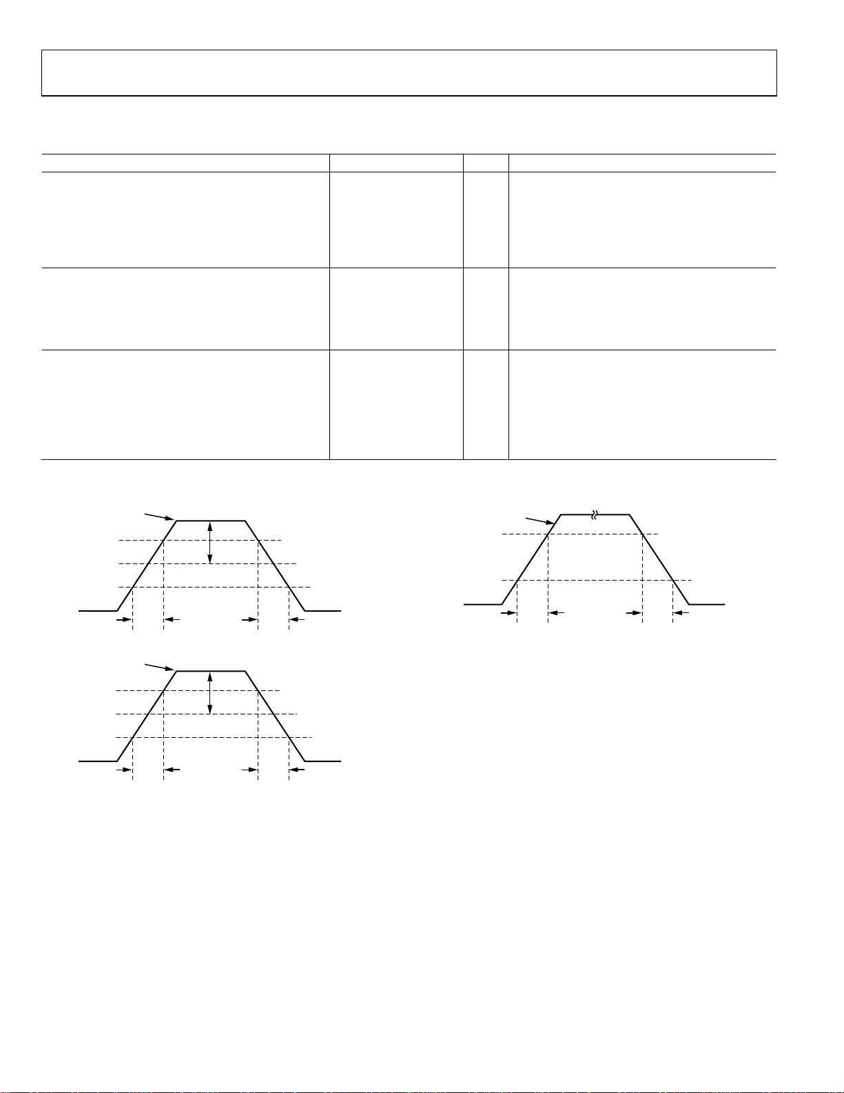
LVPECL (see Figure 2)
Output Rise Time, tRP 170 225 300 ps 20% to 80%, measured differentially
Output Fall Time, tFP 170 230 310 ps 80% to 20%, measured differentially
Skew 20 ps
LVDS (see Figure 3) Termination = 100 Ω differential; C
Output Rise Time, tRL 180 250 340 ps 20% to 80%, measured differentially
Output Fall Time, tFL 180 260 330 ps 80% to 20%, measured differentially
Skew 20 ps
CMOS (see Figure 4)
Output Rise Time, tRC 250 680 950 ps
Output Fall Time, tFC 350 700 1000 ps
Skew 20 ps
Timing Diagrams
DIFFERENTIAL
80%
50%
20%
DIFFERENTIAL
80%
50%
20%
t
RP
Figure 2. LVPECL Timing, Differential
V
OD
LVPECL
V
OD
LVDS
t
FP
09284-002
Termination = 200 Ω to 0 V, ac-coupled to 50 Ω
oscilloscope; C
LOAD
= 5 pF
Between the outputs of the same PLL at the
same frequency. SyncCh01/SyncCh23 set to 1
Between the outputs of the same PLL at the
same frequency; SyncCh01/SyncCh23 set to 1
Termination is high impedance active probe,
total C
LOAD
= 5 pF, R
= 20 kΩ, 20% to 80%
LOAD
Termination is high impedance active probe,
total C
LOAD
= 5 pF, R
= 20 kΩ, 80% to 20%
LOAD
Between the outputs of the same PLL at the
same frequency; SyncCh01/SyncCh23 set to 1
SINGLE-ENDED
80%
20%
t
RC
Figure 4. CMOS Timing, Single-Ended, 5 pF Load
CMOS
t
FC
LOAD
= 5 pF
09284-004
t
RL
t
FL
09284-003
Figure 3. LVDS Timing, Differential
Rev. 0 | Page 12 of 44
Page 13

Data Sheet AD9577
CLOCK OUTPUTS
AC coupling capacitors of 0.1 μF used where appropriate.
Table 8.
Parameter Min Typ Max Unit Test Conditions/Comments
LVPECL CLOCK OUTPUTS
Output Frequency 637.5 MHz
Output Voltage Swing, VOD 610 740 950 mV
Duty Cycle 45 55 %
Output High Voltage, VOH V
Output Low Voltage, VOL V
− 1.24 VS − 0.94 VS − 0.83 V
S
− 2.07 VS − 1.75 VS − 1.62 V
S
LVDS CLOCK OUTPUTS
Output Frequency 637.5 MHz
Differential Output Voltage, VOD 250 350 475 mV
Delta VOD 25 mV
Duty Cycle 45 55 %
Output Offset Voltage, VOS 1.125 1.25 1.375 V
Delta VOS 25 mV
Short-Circuit Current, ISA, ISB 13 24 mA
CMOS CLOCK OUTPUTS
Output Frequency 200 MHz
Output High Voltage, VOH V
− 0.15 V Sourcing 1.0 mA current, outputs static.
S
Output Low Voltage, VOL 0.1 V Sinking 1.0 mA current, outputs static.
Duty Cycle 45 55 %
Load is 200 Ω to GND at output pins, then
ac-coupled to 50 Ω terminated measurement
equipment.
Load is 200 Ω to GND at output pins, then
ac-coupled to 50 Ω terminated measurement
equipment. For differential amplitude, see
Figure 2.
Load is 200 Ω to GND at output pins, then
ac-coupled to 50 Ω terminated measurement
equipment.
Load is 127 Ω/83 Ω potential divider across
supply dc-coupled into 1 MΩ terminated
measurement equipment, outputs static.
Load is 127 Ω/83 Ω potential divider across
supply dc-coupled into 1 MΩ terminated
measurement equipment, outputs static.
Load is ac-coupled to measurement
equipment that provides 100 Ω differential
input termination.
Load is ac-coupled to measurement
equipment that provides 100 Ω differential
input termination. For differential amplitude,
see Figure 3.
Load is ac-coupled to measurement
equipment that provides 100 Ω differential
input termination.
Load is ac-coupled to measurement
equipment that provides 100 Ω differential
input termination.
Load is dc-coupled to a 100 Ω differential
resistor into 1 MΩ terminated measurement
equipment, outputs static.
Load is dc-coupled to a 100 Ω differential
resistor into 1 MΩ terminated measurement
equipment, outputs static.
Load is dc-coupled to a 100 Ω differential
resistor into 1 MΩ terminated measurement
equipment, output shorted to GND.
Termination is high impedance active probe;
total C
LOAD
= 5 pF, R
LOAD
= 20 kΩ.
Rev. 0 | Page 13 of 44
Page 14

AD9577 Data Sheet
POWER
Table 9.
Parameter Min Typ Max Unit Test Conditions/Comments
POWER SUPPLY 3.0 3.3 3.6 V
LVPECL POWER DISSIPATION 1235 1490 mW
1270 1530 mW
LVDS POWER DISSIPATION 1020 1200 mW
1085 1290 mW
CMOS POWER DISSIPATION 1065 1380 mW
1190 1510 mW
POWER CHANGES
Power-Down 1 LVPECL Channel 160 205 mW
Power-Down 1 LVDS Channel 105 155 mW
Power-Down 1 CMOS Channel 130 170 mW Eight single-ended outputs active, C
Typical part configuration, both PLLs enabled for integer-N operation,
= 156.25 MHz, f
f
OUT0
= 125 MHz, f
OUT1
= 100 MHz, f
OUT2
= 33.33 MHz,
OUT3
Na = 100, V0 = 4, D0 = 4, V1 = 4, D1 = 5, Nb = 96, V2 = 4, D2 = 6, V3 = 4,
D3 = 18, 25 MHz crystal used, load is 200 Ω to GND at output pins, then
ac-coupled to 50 Ω terminated measurement equipment
Worst-case part configuration, PLL2 in fractional-N mode, with SSCG
enabled, f
f
= 359.33 MHz, Na = 91, V0 = 3, D0 = 2, V1 = 3, D1 = 2, Nb = 86,
OUT3
= 379.16 MHz, f
OUT0
= 379.16 MHz, f
OUT1
= 359.33 MHz,
OUT2
V2 = 3, D2 = 2, V3 = 3, D3 = 2, FRAC = 300, MOD = 1250, CkDiv = 5,
NumSteps = 77, FracStep = −7, −0.5% downspread at 32 kHz,
25 MHz crystal used, load is 200 Ω to GND at output pins, then
ac-coupled to 50 Ω terminated measurement equipment
Typical part configuration, both PLLs enabled for integer-N operation,
f
= 156.25 MHz, f
OUT0
= 125 MHz, f
OUT1
= 100 MHz, f
OUT2
= 33.33 MHz,
OUT3
Na = 100, V0 = 4, D0 = 4, V1 = 4, D1 = 5, Nb = 96, V2 = 4, D2 = 6, V3 = 4,
D3 = 18, 25 MHz crystal used, load ac-coupled to measurement
equipment that provides 100 Ω differential input termination
Worst-case part configuration, PLL2 in fractional-N mode, with SSCG
enabled, f
= 359.33 MHz, Na = 91, V0 = 3, D0 = 2, V1 = 3, D1 = 2, Nb = 86,
f
OUT3
= 379.16 MHz, f
OUT0
= 379.16 MHz, f
OUT1
= 359.33 MHz,
OUT2
V2 = 3, D2 = 2, V3 = 3, D3 = 2, FRAC = 300, MOD = 1250, CkDiv = 5,
NumSteps = 77, FracStep = −7, −0.5% downspread at 32 kHz,
25 MHz crystal used, load ac-coupled to measurement equipment
that provides 100 Ω differential input termination
Typical part configuration, both PLLs enabled for integer-N operation,
f
= 156.25 MHz, f
OUT0
= 125 MHz, f
OUT1
= 100 MHz, f
OUT2
= 33.33 MHz,
OUT3
Na = 100, V0 = 4, D0 = 4, V1 = 4, D1 = 5, Nb = 96, V2 = 4, D2 = 6, V3 = 4,
D3 = 18, 25 MHz crystal used, eight single-ended outputs active,
= 5 pF
C
LOAD
Worst-case part configuration, PLL2 in fractional-N mode, with SSCG
enabled, f
f
= 179.66 MHz, Na = 91, V0 = 3, D0 = 4, V1 = 3, D1 = 4, Nb = 86,
OUT3
= 189.58 MHz, f
OUT0
= 189.58 MHz, f
OUT1
= 179.66 MHz,
OUT2
V2 = 3, D2 = 4, V3 = 3, D3 = 4, FRAC = 300, MOD = 1250, CkDiv = 5,
NumSteps = 77, FracStep = −7, −0.5% downspread at 32 kHz,
25 MHz crystal used, eight single-ended outputs active, C
LOAD
= 5 pF
Reduction in power due to turning off a channel of one VCO divider,
one output divider, and one output buffer; data for Channel 1, with
typical part configuration, both PLLs enabled for integer-N operation,
f
= 156.25 MHz, f
OUT0
= 125 MHz, f
OUT1
= 100 MHz, f
OUT2
= 33.33 MHz,
OUT3
Na = 100, V0 = 4, D0 = 4, V1 = 4, D1 = 5, Nb = 96, V2 = 4, D2 = 6, V3 = 4,
D3 = 18, 25 MHz crystal used
Load 200 Ω to GND at output pins, and ac-coupled to 50 Ω terminated
measurement equipment
Load ac-coupled to measurement equipment that provides 100 Ω
differential input termination
= 5 pF
LOAD
Rev. 0 | Page 14 of 44
Page 15

Data Sheet AD9577
CRYSTAL OSCILLATOR
Table 10.
Parameter Min Typ Max Unit Test Conditions/Comments
CRYSTAL SPECIFICATION Fundamental mode
Frequency 19.44 25 27 MHz Reference divider, R = 1, only
ESR 50 Ω
Load Capacitance 14 pF
Phase Noise −135 dBc/Hz 1 kHz offset
Stability −50 +50 ppm
REFERENCE INPUT
Table 11.
Parameter Min Typ Max Unit Test Conditions/Comments
CLOCK INPUT (REFCLK)
Input Frequency 19.44 25 27 MHz Reference divider, R = 1
38.88 50 54 MHz Reference divider, R = 2
Input High Voltage 2.0 V
Input Low Voltage 0.8 V
Input Current −1.0 +1.0 μA
Input Capacitance 2 pF
CONTROL PINS
Table 12.
Parameter Min Typ Max Unit Test Conditions/Comments
INPUT CHARACTERISTICS
SSCG, MAX_BW, and MARGIN
SSCG, MAX_BW, and MARGIN have a 30 kΩ internal
pull-down resistor
Logic 1 Voltage 2.0 V
Logic 0 Voltage 0.8 V
Logic 1 Current 240 μA
Logic 0 Current 40 μA
REFSEL REFSEL has a 30 kΩ internal pull-up resistor
Logic 1 Voltage 2.0 V
Logic 0 Voltage 0.8 V
Logic 1 Current 70 μA
Logic 0 Current 240 μA
I2C DC CHARACTERISTICS LVCMOS; the SCL and SDA pins only, see Figure 48
Input Voltage High 0.7 Vcc V
Input Voltage Low 0.3 Vcc V
Input Current −10 +10 μA VIN = 0.1 VCC or VIN = 0.9 VCC
Output Low Voltage 0.4 V VOL with a load current of IOL = 3.0 mA
I2C TIMING CHARACTERISTICS LVCMOS; the SCL and SDA pins only, see Figure 48
SCL Clock Frequency 400 kHz
SCL Pulse Width High
High, t
Low, t
600 ns
HIGH
1300 ns
LOW
Start Condition
Hold Time, t
Setup Time, t
600 ns
HD; STA
600 ns
SU; STA
Data
Setup Time, t
Hold Time, t
Stop Condition Setup Time, t
Bus Free Time Between a Stop and a Start, t
100 ns
SU; DAT
300 ns
HD; DAT
600 ns
SU; STO
1300 ns
BUF
Rev. 0 | Page 15 of 44
Page 16

AD9577 Data Sheet
ABSOLUTE MAXIMUM RATINGS
Table 13.
Parameter
VS to GND −0.3 V to +3.6 V
REFCLK to GND −0.3 V to VS + 0.3 V
LDO to GND −0.3V to VS + 0.3 V
XT1, XT2 to GND −0.3 V to VS + 0.3 V
SSCG, MAX_BW, MARGIN, SCL, SDA,
REFSEL to GND
REFOUT, OUTxP, OUTxN to GND −0.3 V to VS + 0.3 V
Junction Temperature1 150°C
Storage Temperature −65°C to+150°C
Lead Temperature (10 sec) 300°C
1
See the Thermal Characteristics section for θJA.
Rating
−0.3 V to V
+ 0.3 V
S
Stresses above those listed under Absolute Maximum Ratings
may cause permanent damage to the device. This is a stress
rating only; functional operation of the device at these or any
other conditions above those indicated in the operational
section of this specification is not implied. Exposure to absolute
maximum rating conditions for extended periods may affect
device reliability.
THERMAL CHARACTERISTICS
Thermal impedance measurements were taken on a 4-layer
board in still air in accordance with EIA/JESD51-7.
Table 14. Thermal Resistance
Package Type θJA
40-Lead LFCSP 27.5 °C/W
Unit
ESD CAUTION
Rev. 0 | Page 16 of 44
Page 17

Data Sheet AD9577
PIN CONFIGURATION AND FUNCTION DESCRIPTIONS
OUT0N
MAX_BW
TST2A
40
39
OUT0P
GND
GND
SCL
VSVA
36
37
38
SDA
VSOB0A
32
31
33
34
35
1VSCA
2VSI2C
3REFOUT
4VSREFOUT
5VSX
6REFCLK
7XT2
8XT1
9REFSEL
10VSCB
NOTES
1. THE EXPOSED PADDLE ON THIS PACKAGE IS AN ELECTRI CAL CONNECTION
AS WELL AS A THERMAL ENHANCEMENT. FOR T HE DEVI CE TO FUNCTIO N
PROPERLY, THE PADDLE MUST BE ATTACHED TO GROUND (GND). IT IS
RECOMMENDE D THAT A MINIMUM O F NINE VIAS BE USED TO CONNECT THE
PADDLE TO THE P RINTED CI RCUIT BO ARD (PCB) GRO UND PLANE.
PIN 1
INDICATOR
AD9577
TOP VIEW
(Not to Scale)
11
13
12
LDO
TST2B
TST1B
15
14
GND
VSVB
16
GND
Figure 5. Pin Configuration
Table 15. Pin Function Descriptions
Pin No. Mnemonic Description
1 VSCA PLL1 Power Supply.
2 VSI2C I2C Digital Power Supply.
3 REFOUT
4 VSREFOUT
5 VSX
6 REFCLK
7, 8 XT2, XT1
9 REFSEL
10 VSCB
11 TST1B
12 TST2B
13 LDO
14 VSVB
15, 16, 35, 36 GND
17 OUT2N
18 OUT2P
19 VSOB2B
20 MARGIN
21 VSOB3B
22 OUT3N
23 OUT3P
24 VSFB
25 VSM
26 SSCG
27 VSFA
28 OUT1N
CMOS Reference Output.
Reference Output Buffer Power Supply.
Crystal Oscillator and Input Reference Power Supply.
Reference Clock Input. Tie low when not in use.
External 19.44 MHz to 27 MHz Crystal. Leave unconnected when not in use.
Logic Input. Use this pin to select the reference source. Internal 30 kΩ pull-up resistor.
PLL2 Analog Power Supply.
Test Pin. Connect this pin to Pin 13 (LDO).
Test Pin. Connect this pin to Pin 13 (LDO).
This pin is for bypassing the PLL2 LDO to ground with a 220 nF capacitor.
PLL2 VCO Power Supply.
Ground.
LVPECL/LVDS/CMOS Clock Output.
LVPECL/LVDS/CMOS Clock Output.
Output Port OUT2 Power Supply.
Logic 1 sets the margining frequency on the clock output pins. Internal 30 kΩ pull-down resistor.
Output Port OUT3 Power Supply.
LVPECL/LVDS/CMOS Clock Output.
LVPECL/LVDS/CMOS Clock Output.
PLL2 Analog Power Supply.
PLL2 Digital Power Supply.
Logic 1 enables spread spectrum operation of PLL2. Internal 30 kΩ pull-down resistor.
PLL1 Analog Power Supply.
LVPECL/LVDS/CMOS Clock Output.
29 OUT1P LVPECL/LVDS/CMOS Clock Output.
30 VSOB1A
29 OUT1P
28 OUT1N
27 VSFA
26 SSCG
25 VSM
24 VSFB
23 OUT3P
22 OUT3N
21 VSOB3B
18
19
17
20
OUT2P
OUT2N
MARGIN
VSOB2B
09284-005
Rev. 0 | Page 17 of 44
Page 18

AD9577 Data Sheet
Pin No. Mnemonic Description
30 VSOB1A Output Port OUT1 Power Supply.
31 SDA Serial Data Line for I2C.
32 VSOB0A Output Port OUT0 Power Supply.
33 OUT0N LVPECL/LVDS/CMOS Clock Output.
34 OUT0P LVPECL/LVDS/CMOS Clock Output.
37 SCL Serial Clock for I2C.
38 VSVA PLL1 VCO Power Supply.
39 TST2A Test Pin. Connect this pin to the printed circuit board (PCB) ground plane.
40 MAX_BW
EPAD
Logic 1 widens the loop bandwidth of the fractional-N PLL during spread spectrum. Internal 30 kΩ pulldown resistor.
The exposed paddle on this package is an electrical connection as well as a thermal enhancement. For
the device to function properly, the paddle must be attached to ground (GND). It is recommended that
a minimum of nine vias be used to connect the paddle to the printed circuit board (PCB) ground plane.
Rev. 0 | Page 18 of 44
Page 19

Data Sheet AD9577
–
–
–
–
–
–
TYPICAL PERFORMANCE CHARACTERISTICS
REFOUT AND PLL1 PHASE NOISE PERFORMANCE
100
100
–110
–120
–130
–140
PHASE NOISE (dBc/Hz)
–150
–160
1k 10k 100k 1M 100M10M
FREQUENCY (Hz)
Figure 6. Phase Noise, REFOUT Output, 25 MHz (f
100
–110
–120
–130
–140
PHASE NOISE (dBc/Hz)
–150
= 25 MHz)
XTAL
–110
–120
–130
–140
PHASE NOISE (dBc/Hz)
–150
–160
1k 10k 100k 1M 100M10M
09284-006
FREQUENCY (Hz)
09284-009
Figure 9. Phase Noise, PLL1, OUT0 LVPECL, 100 MHz, Integer-N Mode
= 25 MHz, Na = 100, V0 = 5, D0 = 5)
(f
XTAL
100
–110
–120
–130
–140
PHASE NOISE (dBc/Hz)
–150
–160
1k 10k 100k 1M 100M10M
FREQUENCY (Hz)
Figure 7. Phase Noise, PLL1, OUT0 LVPECL, 106.25 MHz, Integer-N Mode
= 25 MHz, Na = 102, V0 = 4, D0 = 6)
(f
XTAL
80
–90
–100
–110
–120
–130
–140
PHASE NOISE (dBc/Hz)
–150
–160
–170
1k 10k 100k 1M 100M10M
FREQUENCY (Hz)
Figure 8. Phase Noise, PLL1, OUT0 LVPECL, 156.25 MHz Integer-N Mode
= 25 MHz, Na = 100, V0 = 4, D0 = 4)
(f
XTAL
09284-007
09284-008
Rev. 0 | Page 19 of 44
–160
1k 10k 100k 1M 100M10M
FREQUENCY (Hz)
Figure 10. Phase Noise, PLL1, OUT0 LVPECL, 125 MHz, Integer-N Mode
= 25 MHz, Na = 100, V0 = 4, D0 = 5)
(f
XTAL
80
–90
–100
–110
–120
–130
–140
PHASE NOISE (dBc/Hz)
–150
–160
–170
1k 10k 100k 1M 100M10M
FREQUENCY (Hz)
Figure 11. Phase Noise, PLL1, OUT0 LVPECL, 625 MHz, Integer-N Mode
= 25 MHz, Na = 100, V0 = 2, D0 = 2)
(f
XTAL
09284-010
09284-011
Page 20

AD9577 Data Sheet
–
–
–
–
–
–
PLL2 PHASE NOISE PERFORMANCE
110
110
–120
–130
–140
PHASE NOISE (dBc/Hz)
–150
–160
1k 10k 100k 1M 100M10M
FREQUENCY (Hz)
Figure 12. Phase Noise, PLL2, OUT2 LVPECL, 100 MHz, Integer-N Mode
= 25 MHz, Nb = 100, V2 = 5, D2 = 5)
(f
XTAL
100
–110
–120
–130
–140
PHASE NOISE (dBc/Hz)
–150
–120
–130
–140
PHASE NOISE (dBc/Hz)
–150
–160
1k 10k 100k 1M 100M10M
09284-012
FREQUENCY (Hz)
09284-015
Figure 15. Phase Noise, PLL2, OUT2 LVPECL, 106.25 MHz, Integer-N Mode
= 25 MHz, Nb = 102, V2 = 4, D2 = 6)
(f
XTAL
90
–100
–110
–120
–130
–140
PHASE NOISE (dBc/Hz)
–150
–160
1k 10k 100k 1M 100M10M
FREQUENCY (Hz)
Figure 13. Phase Noise, PLL2, OUT2 LVPECL, 156.25 MHz, Integer-N Mode
(f
= 25 MHz, Nb = 100, V2 = 4, D2 = 4)
XTAL
100
–110
–120
–130
–140
PHASE NOISE (dBc/Hz)
–150
–160
1k 10k 100k 1M 100M10M
FREQUENCY (Hz)
Figure 14. Phase Noise, PLL2, OUT2 LVPECL, 155.52 MHz, Fractional-N Mode
= 25 MHz, Nb = 99, FRAC = 333, MOD = 625, V2 = 2, D2 = 8), Spurs
(f
XTAL
Disabled
Rev. 0 | Page 20 of 44
–160
1k 10k 100k 1M 100M10M
09284-013
FREQUENCY (Hz)
09284-016
Figure 16. Phase Noise, PLL2, OUT2 LVPECL, 625 MHz, Integer-N Mode
(f
= 25 MHz, Nb = 100, V2 = 2, D2 = 2)
XTAL
90
–100
–110
–120
–130
–140
PHASE NOISE (dBc/Hz)
–150
–160
1k 10k 100k 1M 100M10M
09284-014
FREQUENCY (Hz)
09284-017
Figure 17. Phase Noise, PLL2, OUT2 LVPECL, 622.08 MHz, Fractional-N Mode
= 25 MHz, Nb = 99, FRAC = 333, MOD = 625, V2 = 2, D2 = 2), Spurs
(f
XTAL
Disabled
Page 21

Data Sheet AD9577
A
A
OUTPUT JITTER
480
475
470
465
460
455
450
TED RMS PHASE JITTER (fs)
445
440
INTEGR
435
430
86 87 88 89 90 91 92 93 94 95 96 97 98 99 101100 102
Na
Figure 18. Typical Integrated Random Phase Jitter in fs rms for PLL1 and
OUT0P LVPECL as Feedback Divider Value Na Swept (f
= 25 MHz, V0 = 5,
XTAL
D0 = 5)
09284-018
500
490
480
470
460
TED RMS PHASE JITTER (fs)
450
INTEGR
440
85 86 87 88 89 90 91 92 93 94 95 96 97 98 99 100 101 102 103
Nb
Figure 19. Typical Integrated Random Phase Jitter in fs rms for PLL2 and
OUT2P LVPECL as Feedback Divider Value Nb Swept
= 25 MHz, V2 = 5, D2 = 5, Integer-N Mode)
(f
XTAL
09284-021
Rev. 0 | Page 21 of 44
Page 22

AD9577 Data Sheet
V
V
V
V
V
TYPICAL OUTPUT SIGNAL
200mV/DI
5ns/DIV
Figure 20 Typical LVPECL Differential Output Trace, 156.25 MHz
100mV/DI
5ns/DIV
Figure 21. Typical LVDS Differential Output Trace, 156.25 MHz
200mV/DI
09284-024
1ns/DIV
09284-027
Figure 23. Typical LVPECL Differential Output Trace, 625 MHz
100mV/DI
09284-025
1ns/DIV
09284-028
Figure 24. Typical LVDS Differential Output Trace, 625 MHz
500mV/DIV
1ns/DIV
Figure 22. Typical CMOS Output Trace, 200MHz
09284-026
500mV/DI
10ns/DIV
Figure 25. Typical REFOUT Output Trace, 25 MHz
09284-029
Rev. 0 | Page 22 of 44
Page 23

Data Sheet AD9577
3.5
3.4
3.3
3.2
3.1
3.0
2.9
2.8
2.7
SINGLE -ENDED OUT PUT SWI NG (V)
2.6
2.5
0218016014012010080604020
0.5pF LOAD
5.2pF LOAD
10.5pF LOAD
FREQUENCY (MHz)
00
Figure 26. CMOS Single-Ended, Peak-to-Peak Output Swing vs. Frequency,
for Loads of 0.5 pF, 5.2 pF, and 10.5 pF, Measured with a Tektronix P7313
Active Probe
1.8
1.7
1.6
1.5
900
800
700
600
500
400
DIFFERENTIAL PEAK-TO-PEAK OUTPUT SWING (V)
0 100 200 300 400 500 600
09284-030
FREQUENCY ( MHz)
09284-032
Figure 28. LVDS Differential, Peak-to-Peak Output Swing vs. Frequency
1.4
1.3
1.2
DIFFERENTIAL PEAK-TO-PEAK OUTPUT SWING (V)
0 100 200 300 400 500 600
FREQUENCY (MHz)
Figure 27. LVPECL Differential, Peak-to-Peak Output Swing vs. Frequency
09284-031
Rev. 0 | Page 23 of 44
Page 24

AD9577 Data Sheet
TYPICAL SPREAD SPECTRUM PERFORMANCE CHARACTERISTICS
100.1
100.0
99.9
99.8
99.7
FREQUENCY (M Hz)
99.6
99.5
99.4
TIME (10µ s/DIV)
Figure 29. Typical Spread Spectrum Frequency Modulation Profile OUT2,
Nb = 96, FRAC = 0, MOD = 1000, CkDiv = 7, NumSteps = 59, FracStep = −8,
= 100 MHz with −0.5% Downspread at 30.2 kHz, MAX_BW set to 0
f
OUT
10
UNMODULATED
CLOCK SPECTRUM
0
MODULATED
–10
–20
–30
–40
POWER (d Bm)
–50
–60
–70
–80
CLOCK
99.00 100.50100.25100.0099.7599.5099.25
FREQUENCY (MHz)
Figure 30. Typical Nonspread and Spread Spectrum Power Spectra, OUT2,
Nb = 96, FRAC = 0, MOD = 1000, CkDiv = 7, NumSteps = 59, FracStep = −8,
= 100 MHz with −0.5% Downspread at 30.2 kHz, MAX_BW set to 0,
f
OUT
First Harmonic Shown, Spectrum Analyzer Resolution Bandwidth =10 kHz,
Maximum Hold On
09284-033
09284-034
0
–10
–20
–30
–40
–50
POWER (d Bm)
–60
–70
–80
–90
695 701699697
FREQUENCY (M Hz)
09284-035
Figure 31. Typical Nonspread and Spread Spectrum Power Spectra, OUT2,
Nb = 96, FRAC = 0, MOD = 1000, CkDiv = 7, NumSteps = 59, FracStep = −8,
= 100 MHz with −0.5% Downspread at 30.2 kHz, MAX_BW set to 0,
f
OUT
Seventh Harmonic Shown, Spectrum Analyzer Resolution Bandwidth =
120 kHz, Maximum Hold On
Rev. 0 | Page 24 of 44
Page 25

Data Sheet AD9577
TERMINOLOGY
Phase Jitter and Phase Noise
An ideal sine wave can be thought of as having a continuous
and even progression of phase with time from 0° to 360° for each
cycle. Actual signals, however, display a certain amount of
variation from ideal phase progression over time, which is
called phase jitter. Although many causes can contribute
to phase jitter, one major cause is random noise, which is
characterized statistically as being Gaussian (normal) in
distribution.
This phase jitter leads to a spreading out of the energy of the
sine wave in the frequency domain, producing a continuous
power spectrum. This power spectrum is usually reported as
a series of values whose units are dBc/Hz at a given offset in
frequency from the sine wave (carrier). The value is a ratio
(expressed in dB) of the power contained within a 1 Hz bandwidth with respect to the power at the carrier frequency. For each
measurement, the offset from the carrier frequency is also given.
It is meaningful to integrate the total power contained within
some interval of offset frequencies (for example, 12 kHz to
20 MHz). This is called the integrated phase noise over that
frequency offset interval and can be readily related to the time
jitter due to the phase noise within that offset frequency interval.
Phase noise has a detrimental effect on error rate performance
by increasing eye closure at the transmitter output and reducing
the jitter tolerance/sensitivity of the receiver.
Time Jitter
Phase noise is a frequency domain phenomenon. In the
time domain, the same effect is exhibited as time jitter. When
observing a sine wave, the time of successive zero crossings
vary. In a square wave, the time jitter is seen as a displacement
of the edges from their ideal (regular) times of occurrence. In
both cases, the variations in timing from the ideal are the time
jitter. Because these variations are random in nature, the time
jitter is specified in units of seconds root mean square (rms) or
1 sigma of the Gaussian distribution.
Additive Phase Noise
It is the amount of phase noise that is attributable to the device
or subsystem being measured. The phase noise of any external
oscillators or clock sources has been subtracted. This makes it
possible to predict the degree to which the device affects the
total system phase noise when used in conjunction with the
various oscillators and clock sources, each of which contributes
its own phase noise to the total. In many cases, the phase noise
of one element dominates the system phase noise.
Additive Time Jitter
It is the amount of time jitter that is attributable to the device
or subsystem being measured. The time jitter of any external
oscillators or clock sources has been subtracted. This makes it
possible to predict the degree to which the device will affect the
total system time jitter when used in conjunction with the
various oscillators and clock sources, each of which contributes
its own time jitter to the total. In many cases, the time jitter of
the external oscillators and clock sources dominates the system
time jitter.
Random Jitter Measurement
AD9577, the rms jitter measurements are made by
On the
integrating the phase noise, with spurs disabled. There are two
reasons for this. First, because the part is highly configurable, any
measured spurs are a function of the current programmed state
of the device. For example, there may be a small reference spur at
the PFD frequency present on the output spectrum. If the PFD
operates at 19.44 MHz (which is common for telecommunications
applications), the resulting jitter falls within the normal 12 kHz
to 20 MHz integration bandwidth. When the PFD operates
above 20 MHz, the deterministic jitter is not included in the
measurement. As another example, for PLL2, the value of the
chosen FRAC and MOD values affects the amplitude and
location of a spur, and therefore, it is not possible to configure
the PLL to provide a general measurement that includes spurs.
The second, and more significant reason, is due to the statistical
nature of spurious components. The jitter performance information
of the clock generator is required so that a jitter budget for the
complete communications channel can be established. By
knowing the jitter characteristics at the ultimate receiver, the
data bit error rate (BER) can be estimated to ensure robust data
transfer. The received jitter characteristic consists of random
jitter (RJ), due to random perturbations such as thermal noise,
and deterministic jitter (DJ), due to deterministic perturbations
such as crosstalk spurs. To make an estimate of the BER, the
total jitter peak-to-peak (TJ p-p) value must be known. It is the
total jitter value that determines the amount of eye closure at
the receiver and, consequently, the bit error rate. The TJ p-p
value is specified for a given number of clock edges. For
example, in networking applications, the TJ is specified for 1
clock edges. The equation for the total jitter peak-to-peak is
TJ p-p = DJ p-p + 2 × Q × RJ rms (1)
where the Q factor represents the ratio of the expected peak
deviation to the standard deviation in a Gaussian process for a
given population (of edge crossings). For 1
7.03; therefore, for networking applications, the total jitter peakto-peak is estimated by
TJ p-p = DJ p-p + 14.06 × RJ rms (2)
12
clock edges, Q is
12
Rev. 0 | Page 25 of 44
Page 26

AD9577 Data Sheet
Therefore, to accurately estimate the TJ p-p, separate
measurements of the rms value of the random jitter (RJ rms)
and the peak-to-peak value of the deterministic jitter (DJ p-p)
must be taken. To measure the RJ rms of the clock signal,
integrate the clock phase noise over the desired bandwidth, with
spurs disabled (that is, removed) from the measurement. If the
DJ spurs were included in the measurement, the DJ
contribution would also be multiplied by 14.06 in Equation 2,
leading to a grossly pessimistic estimate of the total jitter. This is
why it is important to measure the integrated jitter with spurs
disabled. Due to the 14.06 factor in Equation 2, the spurious DJ
components on the clock output only have a small impact on
the TJ p-p measurement and, consequently, the system BER
performance. Therefore, it is clear that the DJ component (that
is, the spur) should not be added to the rms value of the random
jitter directly. However, if the phase noise jitter measurement
was preformed with spurs enabled, this is exactly what the
measurement would be reporting. For more background
information, see Fibre Channel, Methodologies for Jitter and
Signal Quality Specification-MJSQ, Rev. 14, June 9, 2004.
Rev. 0 | Page 26 of 44
Page 27

Data Sheet AD9577
DETAILED BLOCK DIAGRAM
XTAL
OSC
FRAC
REFSEL
DIVIDE
1 OR 2
PLL1
PFD
f
PFD/CP
FEEDBACK
DIVIDER
PLL2
PFD/CP
FEEDBACK
DIVIDER
N
0
1
THIRD
ORDER LPF
DIVIDE BY
80 TO 131
N
THIRD
ORDER LPF
DIVIDE BY
80 TO 131
B
SDM
2.15GHz
2.55GHz
A
2.15GHz
2.55GHz
3-BIT
LDO1
VCO
TO
LDO2
VCO
TO
AD9577
VCO
DIVIDERS
V0 D0 FORMAT1
DIVIDE BY
2TO 6
V1 D1
DIVIDE BY
2TO 6
VCO
DIVIDERS
V2 D2 FORMAT2
DIVIDE BY
2TO 6
V3 D3
DIVIDE BY
2TO 6
MOD
OUTPUT
DIVIDERS
DIVIDE BY
1TO 32
DIVIDE BY
1TO 32
OUTPUT
DIVIDERS
DIVIDE BY
1TO 32
DIVIDE BY
1TO 32
CMOS
OUTPUT
BUFFERS
OUTPUT
BUFFERS
REFOUT
LVPECL/LVDS
OR 2 × CMOS
LVPECL/LVDS
OR 2 × CMOS
LVPECL/LVDS
OR 2 × CMOS
LVPECL/LVDS
OR 2 × CMOS
14× VS
4× GND +
PADDLE
22pF
22pF
XT1
XT2
REFCLK
SCL
SDA
MARGIN
SSCG
MAX_BW
I2C
CONTRO L
FRAC_TRIWAVE
f
PFD
CKDIV
FRAC
FRACSTEP
NUMSTEP S
SSCG
GENERATOR
SSCG
TRIWAVE
FRAC_TRIWAVE
LDO
220nF
09284-036
Figure 32. Detailed Block Diagram
Rev. 0 | Page 27 of 44
Page 28

AD9577 Data Sheet
2
EXAMPLE APPLICATION
5MHz XTAL
REFCLK
SCL
SDA
MARGIN
SSCG
MAX_BW
NOTE THAT ANY FREQUE NCIES MAY BE PROGRAMME D.
Achievable application frequencies include (but are not limited to) those listed in Tabl e 16 .
REFSEL
XTAL
OSC
DIVIDE
1 OR 2
THIRD
ORDER LPF
DIVIDER
THIRD
ORDER LPF
DIVIDER
LDO
VCO
2.15GHz
TO
2.55GHz
LDO
VCO
2.15GHz
TO
2.55GHz
PLL1
PFD
f
PFD/CP
FEEDBACK
PLL2
PFD/CP
FEEDBACK
I2C
CONTROL
SPREAD SPECTRUM,
SDM
Figure 33. Example Application
CMOS
DIVIDERS
DIVIDERS
DIVIDERS
DIVIDERS
AD9577
25MHz
CMOS
156.25MHz
LVPECL
125MHz
LVPECL
100MHz LVDS
33.33MHz
2 × CMOS
09284-037
Table 16. Typical Application Frequencies
Applications Frequency (MHz)
Ethernet 25, 62.5, 100, 125, 250
10G Ethernet 155.52, 156.25, 187.5, 161.1328125, 312.5, 622.08, 625
FB-DIMM 133.333, 166.666, 200
Fibre Channel 53.125, 106.25, 212.5, 318.75, 425
10G Fibre Channel 159.375
Inifiniband 125
SAS, SATA 37.5, 75, 100, 120, 150; the AD9577 also meets the −0.5% downspread requirement
Telecomm 19.44, 38.88, 77.76, 155.52, 311.04, 622.08, 627.32962
PCI Express 100, 125, 250; the AD9577 also meets the −0.5% downspread requirement
PCI, PCI-X 33.33, 66.66, 100, 133.33, 200
Video 13.5, 14.318, 17.7, 18, 27, 72, 74.25, 74.25/1.001, 148.5, 148.5/1.001
Wireless Infrastructure 61.44, 122.88, 368.64
Rev. 0 | Page 28 of 44
Page 29

Data Sheet AD9577
FUNCTIONAL DESCRIPTION
On the AD9577, parameters can be programmed over an I2C
bus to provide custom output frequencies, output formats, and
feature selections. However, this programming must be repeated
after every power cycle of the part.
The AD9577 contains two PLLs, PLL1 and PLL2, used for
independent clock frequency generation, as shown in Figure 32.
A shared crystal oscillator and reference clock input cell drive
both PLLs. The reference clock of the PLLs can be selected as
either the crystal oscillator output or the reference input clock.
A reference divider precedes each PLL. When the crystal oscillator
input is selected, these dividers must be set to divide by 1. When
the reference input is selected, these dividers can be set to
divide by 1 or divide by 2, provided that the resulting input
frequency to the PLLs is within the permitted 19.44 MHz to
27 MHz range. Both reference dividers are set to divide by the
same value. Each PLL drives two output channels, producing
four output ports in total for the IC. Each output channel
consists of a VCO divider block, followed by an output divider
block. The output divider blocks each drive with an output
buffer port. Each output buffer port can be configured as a
differential LVDS output, a differential LVPECL output, or two
LVCMOS outputs. Additionally, a CMOS-buffered version
reference clock frequency is available.
The upper PLL in Figure 32, PLL1, is an integer-N PLL. By
setting the feedback divider value (Na), the VCO output
frequency can tuned over the 2.15 GHz to 2.55 GHz range to
integer multiples of the PFD input frequency. By setting each of
the VCO divider (V0 and V1) and output divider (D0 and D1)
values, the VCO frequency can be divided down to the required
output frequency, independently, for each of the output ports,
OUT0 and OUT1. The loop filter required for this PLL is
integrated on chip.
The lower PLL in Figure 32, PLL2, is a fractional-N PLL. This
PLL can optionally operate as an integer-N PLL for optimum
jitter performance. By setting the feedback divider value (Nb)
and the Σ-Δ modulator fractional (FRAC) and modulus (MOD)
values, the VCO output frequency can tune over the 2.15 GHz
to 2.55 GHz range. The VCO frequency is a fractional multiple
of the PFD input frequency. In this way, the VCO frequency can
tune to obtain frequencies that are not constrained to integer
multiples of the PFD frequency. By setting each of the VCO divider
(V2 and V3) and output divider (D2 and D3) values, the VCO
frequency can be divided down to the required output frequency,
independently, for each of the output ports, OUT2 and OUT3.
The loop filters required for this PLL are integrated on chip.
The PLL2 can operate to modulate the output frequency between its
nominal value and a value that is up to −0.5% lower. This provides
spread spectrum modulation up to −0.5% downspread. Spread
spectrum frequency modulation can reduce the peak power output
of the clock source and any circuitry that it drives and lead to
reduced EMI emissions. In the AD9577, the frequency modulation
profile is triangular. The modulation frequency and modulation
range parameters are all programmable.
Both PLLs can be programmed to generate a second independent
frequency map under the control of the MARGIN pin. This
feature can be used to test the frequency robustness of a system.
REFERENCE INPUT AND REFERENCE DIVIDERS
The reference input section is shown in Figure 34. When the
REFSEL pin is pulled high, the crystal oscillator circuit is enabled.
The crystal oscillator circuit needs an external crystal cut to
resonate in fundamental mode in the 19.44 MHz to 27 MHz
range, with 25 MHz being used in most networking applications.
The total load capacitance presented to the crystal should add
up to 14 pF. In the example shown in Figure 34, parasitic trace
capacitance of 1.5 pF and an AD9577 input pin capacitance of
1.5 pF are assumed, with the series combination of the two
22 pF capacitances providing an additional 11 pF. When the
REFSEL pin is pulled low, the crystal oscillator powers down,
and the REFCLK pin must provide a good quality reference clock
instead. Either a dc-coupled LVCMOS level signal or an ac-coupled
square wave can drive this single-ended input, provided that an
external potential divider is used to bias the input at V
The output of the crystal oscillator and reference input circuitry
is routed to a reference divider circuit to further divide down
the reference input frequency to the PLLs by 1 or 2. When the
crystal oscillator circuit is used, the dividers must be set to
divide by 1. The input frequency to the PLLs must be in the
19.44 MHz to 27 MHz range. The divide ratio is set to 1 by
programming the value of R, Register G0[1], to 0. The divide
ratio is set to 2 by programming the value of R to 1.
XTAL
OSC
REFSEL
DIVIDE
1 OR 2
22pF
22pF
REFCLK
Figure 34. Reference Input Section and Reference Dividers
Table 17. REFSEL (Pin 9) Definition
REFSEL Reference Source
0 REFCLK input
1 Crystal oscillator
/2.
S
TO PLLs
09284-038
Table 18. Reference Divider Setting
R, Register G0[1] Reference Divide Ratio
0 Divide by 1
1 Divide by 2
Rev. 0 | Page 29 of 44
Page 30

AD9577 Data Sheet
V
V
OUTPUT CHANNEL DIVIDERS
Between each VCO and its associated chip outputs, there are
two divider stages: a VCO divider that has a divide ratio between
2 and 6 and an output divider that can be set to divide between
1 and 32. This cascade of dividers allows a minimum output
channel divide ratio of 2 and a maximum of 192. With VCO
frequencies ranging between 2.15 GHz and 2.55 GHz, the part
can be programmed to spot frequencies over a continuous
frequency range of from 11.2 MHz to 200 MHz, and it can be
programmed to spot frequencies over a continuous frequency
range of 200 MHz and 637.5 MHz, with only a few small gaps.
OUTPUTS
Each output port can be individually configured as either
differential LVPECL, differential LVDS, or two single-ended
LVCMOS clock outputs. The simplified equivalent circuit of the
LVDS outputs is shown in Figure 36.
3.5mA
OUTxP
OUTxN
Table 19. Divider Ratio Setting Registers
Divide
Divider I2C Registers Parameter
Range
Channel 0 VCO divider ADV0[7:5] V0 2 to 6
Channel 1 VCO divider ADV1[7:5] V1 2 to 6
Channel 2 VCO divider BDV0[7:5] V2 2 to 6
Channel 3 VCO divider BDV1[7:5] V3 2 to 6
Channel 0 output divider ADV0[4:0] D0 1 to 321
Channel 1 output divider ADV1[4:0] D1 1 to 321
Channel 2 output divider BDV0[4:0] D2 1 to 321
Channel 3 output divider BDV1[4:0] D3 1 to 321
1
Set to 00000 for divide by 32.
Asserting the SyncCh01 or SyncCh23 bits (Register ADV2[0]
or Register BDV2[0]) allows each PLL output channel to use a
common VCO divider. This feature allows the OUT0/OUT1 and
OUT2/OUT3 output ports to have minimal skew when their
relative output channel divide ratio is an integer multiple.
Duty-cycle correction circuitry ensures that the output duty cycle
remains at 50%.
CO
VCO
DIVIDE R
V0[2:0] D0[4:0]
VCO
DIVIDE R
OUTPUT
DIVIDE R
OUTPUT
DIVIDE R
OUT0
OUT1
3.5mA
Figure 36. LVDS Outputs Simplified Equivalent Circuit
09284-040
The simplified equivalent circuit of the LVPECL outputs is
shown in Figure 37.
3.3
OUTxP
OUTxN
GND
Figure 37. LVPECL Outputs Simplified Equivalent Circuit
09284-041
Output channels (consisting of a VCO divider, output divider, and
an output buffer) can be individually powered down to save power.
Setting PDCH0, PDCH1, PDCH2, and PDCH3 (Register BP0[1:0]
and Register DR1[7:6]) powers down the appropriate channel.
Output buffer combinations of LVDS, LVPECL, and CMOS can be
selected by setting DR1[5:0] as is shown in Tab le 20 and Tab le 21 .
VCO
V1[2:0] D1[4:0]
VCO
DIVIDE R
V2[2:0] D2[4:0]
VCO
DIVIDE R
V3[2:0] D3[4:0]
Figure 35. Output Channel Divider Signal Path
OUTPUT
DIVIDE R
OUTPUT
DIVIDE R
OUT2
OUT3
09284-039
Rev. 0 | Page 30 of 44
Table 20. PLL1 Output Driver Format Control Bits,
Register DR1[2:0]
FORMAT1 (PLL1)
Register DR1[2:0] OUT1P/OUT1N OUT0P/OUT0N
000 LVPECL LVPECL
001 LVDS LVDS
010 2 × CMOS LVPECL
011 2 × CMOS 2 × CMOS
100 2 × CMOS LVDS
101 LVPECL LVDS
110 LVPECL 2 × CMOS
1
111
2 × CMOS 2 × CMOS
1
This indicates that the CMOS outputs are in phase; otherwise, they are in
antiphase.
Page 31

Data Sheet AD9577
V
V
V
Table 21.PLL2 Output Driver Format Control Bits,
Register DR1[5:3]
FORMAT2 (PLL2)
Register DR1[5:3] OUT3P/OUT3N OUT2P/OUT2N
000 LVPECL LVPECL
001 LVDS LVDS
010 2 × CMOS LVPECL
011 2 × CMOS 2 × CMOS
100 2 × CMOS LVDS
101 LVPECL LVDS
110 LVPECL 2 × CMOS
1111 2 × CMOS 2 × CMOS
1
This indicates that the CMOS outputs are in phase; otherwise, they are in
antiphase.
LVDS uses a current mode output stage. The normal value
(default) for this current is 3.5 mA, which yields a 350 mV
output swing across a 100 Ω resistor. The LVDS outputs meet or
exceed all ANSI/TIA/EIA-644 specifications. The LVDS output
buffer should be terminated with a 100 Ω differential resistor
between the receiver input ports (see Figure 38). A recommended
termination circuit for the LVDS outputs is shown in Figure 38.
50Ω
LVDS
Figure 38. LVDS Output Termination
100Ω
50Ω
LVDS
09284-042
See the AN-586 Application Note, LVD S O ut p ut s f o r H i gh Sp ee d
A/D Converters, for more information about LVDS.
In a dc-coupled application, the LVPECL output buffer should
be terminated via a pair of 50 Ω resistors to a voltage of V
− 2 V.
CC
This can be implemented by using potential dividers of 127 Ω
and 83 Ω between the supplies, as shown in Figure 39.
3.3
3.3V
LVPECL
Figure 39. LVPECL DC-Coupled Termination
50Ω
SINGLE-ENDED
(NOT CO UPLED)
50Ω
VT = VDD – 2V
3.3V
127Ω127Ω
LVPECL
83Ω83Ω
09284-043
An alternative LVPECL termination scheme for dc-coupled
applications is shown Figure 40.
50Ω
50Ω
50Ω
LVPECL
09284-044
LVPECL
50Ω
50Ω
Figure 40. LVPECL DC-Coupled Y-Termination
In ac-coupled applications, the LVPECL output stage needs a
pair of 200 Ω pull-down resistors to GND to provide a dc path for
the output stage emitter followers (see Figure 41). The receiver must
provide an additional 50 Ω single-ended input termination.
TERM
0.1µF
LVPECL
0.1µF
200Ω200Ω
Figure 41. LVPECL AC-Coupled Termination
50Ω
50Ω
50Ω50Ω
LVPECL
09284-045
REFERENCE OUTPUT BUFFER
A CMOS buffered copy of the reference input circuit signal is
available at the REFOUT pin. This buffer can be optionally
powered down by setting Register DR2[0], PDRefOut to Logic 0.
PLL1 INTEGER-N PLL
The upper PLL in Figure 32, PLL1, is an integer-N PLL with a
loop bandwidth of 140 kHz. The input frequency to the PLL
from the reference circuit is f
programmed by setting the value for Na, according to
f
= f
VCO1
× Na (3)
PFD
where Na is programmable in the 80 to 131 range. The VCO
output frequency can tune over the 2.15 GHz to 2.55 GHz range to
integer multiples of the PFD input frequency only.
By setting each of the VCO divider (V0 and V1) and output
divider (D0 and D1) values, the VCO frequency can be divided
down to the required output frequency, independently, for each
of the output ports, OUT0 and OUT1. The f
presented to OUT0 can be set according to
OUT
The frequency f
ff
OUT
PFD
×
presented to OUT1 can be set according to
OUT1
Na
×=
×
Na
×=
ff
PFD
0
The loop filters required for this PLL are integrated on chip.
. The VCO frequency, f
PFD
frequency
OUT0
(4)
D0V0
(5)
111D
VCO1
, is
Rev. 0 | Page 31 of 44
Page 32

AD9577 Data Sheet
V
M
PLL1 PHASE FREQUENCY DETECTOR (PFD) AND CHARGE PUMP
The PFD determines the phase difference error between the
reference divider output and the feedback divider output clock
edges. The outputs of this circuit are pulse-width modulated up
and down signal pulses. These pulses drive the charge pump
circuit. The amount of charge delivered from the charge pump to
the loop filter is determined by the instantaneous phase error. The
action of the closed loop is to drive the frequency and phase error
at the input of the PFD toward zero. Figure 42 shows a block
diagram of the PFD/CP circuitry.
3.3
CHARGE
HIGH
REFCLK
D1 Q1
CLR1
UP
PUMP
CP
To determine if both 156.25 MHz and 100 MHz can be derived
from a common f
frequency in the 2.15 GHz to 2.55 GHz
VCO1
range, use the lowest common multiple (LCM) of 156.25 MHz
and 100 MHz to determine the lowest VCO frequency that can
be divided down to provide both of these frequencies.
LCM(156.25 MHz, 100 MHz) = 2.5 GHz (6)
Therefore, set the VCO frequency to 2.5 GHz. With f
PFD
=
25 MHz, from Equation 3, Na must be set to 100.
For 156.25 MHz on Port 0, set
V0 × D0 = 16 (7)
This can be achieved by setting V0 to 4 and D0 to 4. For
100 MHz on Port 1, set
V1 × D1 = 25 (8)
This can be achieved by setting V1 to 5 and D1 to 5. With a
reference frequency of 25 MHz, the reference divider value, R,
must be set to 1 by setting Register G0[1] to 0. Tabl e 22
summarizes the register settings for this configuration.
CLR2
D2 Q2
DOWN
GND
09284-047
HIGH
FEEDBACK
DIVIDER
Figure 42. PFD Circuit Showing Simplified Charge Pump
PLL1 VCO
PLL1 incorporates a low phase noise LC-tank VCO. This VCO
has 32 frequency bands spanning from 2.15 GHz to 2.55 GHz.
At power-up, a VCO calibration cycle begins and the correct band
is selected based on the feedback divider setting (Na). Whenever a
new feedback divider setting is called for, the VCO calibration
process must run by writing 1 followed by 0 to the NewAcq bit,
Register X0[0].
PLL1 FEEDBACK DIVIDER
The feedback divider ratio, Na, is used to set the PLL1 VCO
frequency according to Equation 3. Note that the Na value is set
by adding the offset value of 80 to the value programmed to
Register AF0[5:0], where 80 is the minimum divider Na value.
The maximum Na value is 131. For example, to set Na to 85, the
AF0[5:0] register is set to 5.
SETTING THE OUTPUT FREQUENCY OF PLL1
For example, set the output frequency (f
156.25 MHz, the output frequency (f
and both the reference frequency (f
(f
) to 25 MHz.
PFD
The frequency f
presented to OUT0 can be set according to
OUT0
OUT1
REF
Equation 4.
The frequency f
presented to OUT1 can be set according to
OUT1
Equation 5.
) on Port 0 to
OUT0
) on Port 1 to 100 MHz,
) and the PFD frequency
Table 22. Register Settings for Example PLL1 Configuration
Parameter Divide Value I2C Register Register Value
Na 100 AF0[5:0] 010100
V0 4 ADV0[7:5] 100
D0 4 ADV0[4:0]
V1 5 ADV1[7:5]
D1 5 ADV1[4:0]
00100
101
00101
R 1 G0[1] 1
PLL2 INTEGER/FRACTIONAL-N PLL
The lower PLL in Figure 32, PLL2, is a fractional-N PLL. The
input frequency to the PLL from the reference circuit is f
The VCO frequency, f
, is programmed by setting the values
VCO2
for Nb, FRAC, and MOD according to
FRAC
(9)
VCO
+×=
Nbff
PFD
2
OD
)(
where Nb is programmable in the 80 to 131 range. To provide
the greatest flexibility and accuracy, both the FRAC and MOD
values can be programmed to a resolution of 12 bits, where
FRAC < MOD. The VCO output frequency can tune over the
2.15 GHz to 2.55 GHz range to fractional multiples of the PFD
input frequency.
By setting each of the VCO divider (V2 and V3) and output
divider (D2 and D3) values, the VCO frequency can be divided
down to the required output frequency, independently, for each
of the output ports, OUT2 and OUT3. The f
frequency
OUT2
presented to OUT2 can be set according to
FRAC
Nb
OUT2
+
ff
×=
PFD
MOD
D2V2
×
)(
(10)
PFD
.
Rev. 0 | Page 32 of 44
Page 33

Data Sheet AD9577
The f
The loop filters required for this PLL are integrated on chip.
By setting the FRAC value to 0, powering down the SDM by setting
Register ABF0[4] to 1, and turning the bleed current off by setting
Register BP0[2] = 0, PLL2 can operate as an integer-N PLL.
Equation 10 and Equation 11 are still used to set the output
frequencies for f
improved performance in terms of phase noise, spurs, and jitter.
PLL2 PHASE FREQUENCY DETECTOR (PFD) AND CHARGE PUMP
The PLL2 PFD and charge pump is the same as that described
in the PLL1 Phase Frequency Detector (PFD) and Charge Pump
section. When operating in fractional-N mode, a charge pump
bleed current should be enabled to linearize the PLL transfer
function and, therefore, to minimize spurs due to the operation
of the Σ-Δ modulator. Bleed is enabled by setting Register BP0[2].
PLL2 LOOP BANDWIDTH
The normal PLL loop bandwidth is 50 kHz. When the SSCG input
pin is asserted, the loop bandwidth switches from 50 kHz to
125 kHz, which prevents the triangle-wave modulation waveform
from being overly filtered by the PLL. When the MAX_BW input
pin is set high, it forces the PLL bandwidth to be 250 kHz
instead of 125 kHz.
PLL2 VCO
PLL2 incorporates a low phase noise LC-tank VCO. This VCO
has 32 frequency bands spanning from 2.15 GHz to 2.55 GHz.
At power-up, a VCO calibration cycle begins and the correct band
is selected based on the feedback divider setting (Nb). Whenever a
new feedback divider setting is called for, the VCO calibration
process must run by writing 1 followed by 0 to the NewAcq bit,
Register X0[0].
PLL2 FEEDBACK DIVIDER
The Nb feedback divider ratio is used to set the PLL2 VCO
frequency according to Equation 9. Note that the Nb value is set
by adding the decimal value programmed to Register BF3[5:0]
to a decimal value of 80, where the minimum divider Nb value
is 80. The maximum Nb value is 131. For example, to set Nb to 85,
Register BF3[5:0] is set to 5.
PLL2 Σ-Δ MODULATOR
When operating in fractional-N mode only, PLL2 uses a thirdorder, multistage noise shaping (MASH) Σ-Δ modulator (SDM)
to adjust the feedback divider ratio. The programmed Nb value
can be adjusted over the −4 to +3 range on every rising clock
edge from the feedback divider output (typically 25 MHz for
networking applications). In this way, the average feedback divide
ratio is adjusted to be a noninteger value, allowing for a VCO
frequency that is a fractional multiple of the PFD frequency to be
frequency presented to OUT3 can be set according to
OUT3
FRAC
Nb
OUT3
+
ff
×=
PFD
and f
OUT2
)(
MOD
×
OUT3
(11)
D3V3
. Operation in this mode provides
synthesized. By setting the FRAC and MOD values of the SDM, the
PLL2 VCO frequency can be set according to Equation 9. The SDM
must be turned on by setting PD_SDM to 0, Register ABF0[4].
12-Bit Programmable Modulus (MOD) and Fractional (FRAC) Values
Unlike most other fractional-N PLLs, the AD9577 allows users to
program the modulus over a 12-bit range, which means they can
set up the part in many different configurations. It also usually
means that, in most applications, it is possible to design the PLL
to achieve the desired output frequency multiplication with 0 ppm
frequency error. The MOD value is set by setting Register BF1[3:0]
and Register BF2[7:0]. The FRAC value is set by setting
Register BF0[7:0] and Register BF1[7:4].
Bleed Current
When the SDM is operational (Register ABF0[4] set to 0), bleed
current should be enabled (Register BP0[2] set to 1), which
increases the in-band phase noise but reduces the fractional spur
amplitudes. All fractional-N jitter data is reported with bleed = 1.
If bleed = 0 in fractional-N mode, the rms jitter decreases
significantly; however, the fractional spur amplitudes increase.
When PLL2 operates in integer-N mode, the bleed current
should be disabled to improve the PLLs in-band phase noise.
SPUR MECHANISMS
This section describes the three different spur mechanisms that
arise with a fractional-N PLL: fractional spurs, integer boundary
spurs, and reference spurs.
Fractional Spurs
The fractional interpolator in the AD9577 is a third-order SDM
with a modulus that is programmable to any integer value from
50 to 4095. The SDM is clocked at the PFD reference rate (f
allows PLL output frequencies to be synthesized at a channel step
resolution of f
modulator appears as fractional spurs. The interval between spurs
is f
digital Σ-Δ modulator. For the third-order modulator used in the
AD9577, the repeat length depends on the value of MOD, as
listed in Table 2 3.
Table 23. Fractional Spur Frequencies
Condition
If MOD is divisible by 2, but not 3 2 × MOD f
If MOD is divisible by 3, but not 2 3 × MOD f
If MOD is divisible by 6 6 × MOD f
Otherwise MOD f
Rev. 0 | Page 33 of 44
/MOD. The quantization noise from the Σ-Δ
PFD
/L, where L is the repeat length of the code sequence in the
PFD
Repeat
Length Spur Interval
/(2 × MOD)
PFD
/(3 × MOD)
PFD
/(6 × MOD)
PFD
/MOD
PFD
PFD
) that
Page 34

AD9577 Data Sheet
Integer Boundary Spurs
Another mechanism for fractional spur creation is the interactions
between the RF VCO frequency and the reference frequency.
When these frequencies are not integer related (the point of a
fractional-N synthesizer), spur sidebands appear on the VCO
output spectrum at an offset frequency that corresponds to the
beat note or difference frequency, between an integer multiple
of the reference and the VCO frequency. These spurs are attenuated
by the loop filter and are more noticeable on channels close to
integer multiples of the reference where the difference frequency
can be inside the loop bandwidth; therefore, the name integer
boundary spurs.
Reference Spurs
Reference spurs occur for both integer-N and fractional-N
operation. Reference spurs are generally not a problem in
fractional-N synthesizers because the reference offset is far
outside the loop bandwidth. However, any reference feedthrough mechanism that bypasses the loop may cause a problem.
Feedthrough of low levels of on-chip reference switching noise,
through the reference input or output pins back to the VCO, can
result in noticeable reference spur levels. In addition, coupling
of the reference frequency to the output clocks can result in beat
note spurs. PCB layout needs to ensure adequate isolation between
VCO/LDO supplies, the output traces, and the input or output
reference to avoid a possible feedthrough path on the board. If
the reference output clock (REFCLK) is not required, it should
be powered down to minimize potential board coupling. The
SDM digital circuitry is clocked by the reference clock. The
SDM is enabled when PLL2 is in fractional-N mode. When PLL2
is in fractional-N mode, the switching noise at the reference
frequency may result in increased spurs levels at the outputs.
OPTIMIZING PLL PERFORMANCE
Because the AD9577 can be configured in many ways, some guidelines should be followed to ensure that the high performance is
maintained. For both PLLs, there can be a small advantage in
choosing a lower VCO frequency because the VCO phase noise
tends to be slightly better at lower frequencies. Both VCOs should
not operate at the same frequency because this degrades jitter
performance. The two VCO frequencies should differ by at least
2 MHz. The following guidelines apply to PLL2 operating in
fractional-N mode only. If possible, denominators that have factors
of 2, 3, or 6 should be avoided because they can produce slightly
higher subfractional spur components. Avoid low and high
fractions (that is, FRAC/MOD close to 1/MOD or (MOD − 1)/
MOD) because these are more susceptible to larger fractional
spur components and integer boundary spurs. Avoid creating a
low valued beat frequency between the output frequency and the
PFD frequency to minimize the risk of low offset beat frequency
spurs. For example, setting f
can create an output spur at 10 kHz offset to 100.01 MHz,
depending on board layout. Choosing a smaller MOD value results
in fractional spurs that are at a higher frequency and, consequently,
are better filtered by the PLL loop filter bandwidth of 50 kHz.
= 25 MHz, and f
PFD
= 100.01 MHz
OUT
Rev. 0 | Page 34 of 44
SETTING THE OUTPUT FREQUENCY OF PLL2
For example, to set the output frequency (f
155.52 MHz and the output frequency (f
38.88 MHz using a reference frequency (f
frequency (f
The frequency f
) of 25 MHz, do the following.
PFD
presented to OUT2 can be set according to
OUT2
Equation 10.
The frequency f
presented to OUT3 can be set according to
OUT3
Equation 11.
In this case, both 155.52 MHz and 38.88 MHz can be derived
from the same VCO frequency because they are related by a
factor of 4.
The next step is to determine what the required values of f
V2, and D2 are to divide down to 155.52 MHz. Tab le 2 4 shows
the available options.
Table 24. Suitable Values of f
= 155.52 MHz
f
OUT2
f
(MHz) V2 × D2 f
OUT2
155.52 14 2.17728
155.52 15 2.3328
155.52 16 2.48832
Choose a f
value of 2.48832 GHz. Next, determine that the
VCO2
and V2 × D2, to Achieve
VCO2
(GHz)
VCO2
multiplication ratio (Nb + FRAC/MOD) required to multiply a
f
of 25 MHz up to 2.48832 GHz is 99.5328. Therefore, Nb must
PFD
be set to 99 and (FRAC/MOD) = 0.5328. To convert 0.5328 to a
fraction, 0.5328 can be the same as 5328/10000. This fraction
can then be reduced to the lowest terms by dividing both the
numerator and denominator by 16, where 16 is the greatest
common divisor (GCD) of the 5328 and 10,000. This results in
a solution for FRAC/MOD = 333/625.
For 155.52 MHz on Port 2, set V2 × D2 = 16. This can be achieved
by setting V2 to 4 and D2 to 4. For 38.88 MHz on Port 3, set V3
× D3 = 64. This can be achieved by setting V3 to 4 and D3 to
16. With a reference frequency of 25 MHz, the reference divider
value, R, must be set to 1 by setting Register G0[1] to 0. Because
both channels use VCO divide values of 4on V2 and V3, SyncCh23,
Register BDV2[0], can be set to 1 to ensure that the clock edges
on Port 2 and Port 3 are synchronized. Tab le 2 5 summarizes the
register setting for this configuration.
Table 25. Registers Setting for Example PLL2 Configuration
Parameter Value I2C Register Register Value
Nb 99 BF3[5:0] 010011
FRAC 333 BF0[7:0], BF1[7:4] 000101001101
MOD 625 BF1[3:0], BF2[7:0] 001001110001
V2 4 BDV0[7:5] 100
D2 4 BDV0[4:0] 00100
V3 4 BDV1[7:5] 100
D3 16 BDV1[4:0] 10000
R 1 G0[1] 0000
SyncCh23 1 BDV2[0] 1
) on Port 2 to
OUT2
) on Port 3 to
OUT3
) and PFD
REF
VCO2
,
Page 35

Data Sheet AD9577
FREQUENCY
f
– 0.5%
VCO
THIRD
ORDER LPF
DIVIDE BY
80 TO 131
N
B
SDM
GENERATO R
Modulation, f
f
VCO
VCO
VCO
2.15GHz
TO
2.55GHz
3-BIT
SSCG
TRIWAVE
MOD
FRAC_TRIW AVE
= 25 MHz
PFD
TIME
TIME
MARGINING
By asserting the MARGIN pin, a second full frequency map can
be applied to the output ports. The values for the Na, V0, D0,
V1, and D1 parameters, and the Nb, FRAC, MOD, V2, D2, V3,
D3 parameters must be programmed over the I
2
C, although default
values exist. There are some limitations: the output buffer signal
formats cannot be changed, and the PLL2 fractional-N settings,
such as power-down of the SDM, and bleed settings cannot be
changed. The margining feature can be used to set higher than
nominal frequencies on each of the ports to test system robustness.
When the MARGIN pin signal level is changed, a new frequency
acquisition is performed.
SPREAD SPECTRUM CLOCK GENERATION (SSCG)
By asserting the SSCG (spread spectrum clock generator) pin,
PLL2 operates in spread spectrum mode, and the output
frequency modulates with a triangular profile. As the clock
signal energy spreads out over a range of frequencies, it reduces
the peak power at any one frequency when observed with a
spectrum analyzer through a resolution bandwidth filter. This
result improves the radiated emissions from the part and from
the devices that receive its clock.
The triangular-wave modulation is implemented by controlling
the divide ratio of the feedback divider. This is achieved by
ramping the fractional word to the SDM. Figure 43 shows an
example implementation. The PFD frequency, f
The starting VCO frequency, f
, is 25 MHz × (99 + 3072/4096),
VCO
giving 2.49375 GHz. By continuously ramping the FRAC word
down and up, this frequency is periodically reduced to 25 MHz ×
(99 + 1029/4096) = 2.481281 GHz. This results in a triangular
frequency modulation profile, with a peak downspread (that is,
peak percentage frequency reduction) of −0.5%. By controlling
the step size, number of steps, and the step rate, the modulation
frequency is adjusted.
, is 25 MHz.
PFD
f
PFD
FRAC_TRIW AVE
PFD/CP
FEEDBACK
DIVIDER
FRAC
0
1
SSCG
FRAC_TRI WAVE = 3072
FRAC_TRI WAVE = 1029
f
PFD
CKDIV
FRAC
FRACSTEP
NUMSTEPS
Figure 43. Spread Spectrum Clock Generator with Triangular Wave
Basic Spread Spectrum Programming
The SSCG is highly programmable; however, most applications
require that the frequency modulation rate be between 30 kHz
and 33 kHz and that the peak frequency deviation be −0.5%
downspread. The AD9577 supports downspread only, with a
maximum deviation of −0.5%.
The key parameters (which are not themselves registers) that
define the frequency modulation profile include the following:
• f
, which is the frequency of the modulation waveform.
MOD
• FracRange, which determines the peak frequency deviation
by setting the maximum change in the FRAC value from
the nominal.
09284-048
The following equations determine the value of these parameters:
where the following are programmable registers:
• NumSteps is the number of fractional word steps in half the
• FracStep is the value of the fractional word increment/
• CkDiv is the integer value by which the reference clock
• f
Rev. 0 | Page 35 of 44
FracRange = FracStep × NumSteps (12)
f
f
MOD
PFD
(13)
CkDivNumSteps
××=2
triwave period.
decrement, while traversing the tri-wave.
frequency is divided to determine the update rate of the
triangular-wave generator, that is, the step update rate.
is the PFD frequency.
PFD
Page 36

AD9577 Data Sheet
M
Tabl e 2 6 shows the relevant register names and programmable
ranges.
Table 26. Registers Used to Program SSCG Operation
Parameter
NumSteps
FracStep
CkDiv BS3[6:0] +2 to +127
Register Name Range
BS2[7:0], BS3[7] +1 to +511
BS1[7:0]
−128 to 0
Because the register values need to be expressed as integers,
there are no guaranteed exact solutions; therefore, some
approximations and trade-offs must be made. The fact that
neither FracRange nor f
needs to be exact is exploited.
MOD
Note that the SSCG pin must be toggled every time the SSCG
parameters are adjusted for the changes to take effect.
Worked Example: Programming for f
Downspread = −0.5%, f
= 25 MHz
PFD
= 31.25 kHz,
MOD
Assume Nb = 100, MOD = 625, and FRAC = 198. In addition, a
large number of frequency steps are desired to cover −0.5%. The
objective is to find values for FracStep, NumSteps, and CkDiv
that result in the required frequency modulation profile.
The total feedback divider ratio is
N
= Nb +
TOT
FRAC
= 100 + 198/625 = 62,698/625
OD
FracRange is set to −0.5% of 62,698, which results in an ideal
value of −313.5.
By rearranging Equation 12 and Equation 13, it results in
CkDivFracStep
⎜
⎝
f
⎛
2
⎜
×=
Putting in the values for FracRange, f
PFD
MOD
××
fFracRange
MOD
, and f
⎞
⎟
(14)
⎟
⎠
from the
PFD
previous information, the following results:
FracStep = CkDiv × (−0.78375) (15)
An approximate solution must be found to Equation 15 that
produces an integer value for CkDiv, which gives a value that is
very close to an integer for FracStep. In this case, considering
CkDiv values in the range of 2 to 10 gives the FracStep values
shown in Tab l e 2 7 .
Table 27. CkDiv and FracStep Values Used in Worked Example
Ideal
CkDiv
2 −1.5675 −2 21.6%
3 −2.35125 −2
4 −3.135 −3
5 −3.91875 −4
6 −4.7025 −5 6.0%
7 −5.48625 −5
8 −6.27 −6 4.5%
9 −7.05375 −7
10 −7.8375 −8 2.0%
FracStep Rounded FracStep
FracStep Error
17.6%
4.5%
2.0%
9.7%
0.77%
Both CkDiv and NumSteps must be integers. To minimize error,
CkDiv = 9 and FracStep = −7 was chosen. With a target for
FracRange = −313.5, Equation 12 is used to find the ideal value of
NumSteps = 44.79, which is rounded to 45. From Equation 12,
the actual used value for FracRange is
FracRange = −7 × 45 = −315
The accuracy of this solution needs to be verified. Putting the
derived values into Equation 13 gives
f
MOD
f
=
2
PFD
××
CkDivNumSteps
MHz25
=
9452
××
kHz30.86
=
In addition, the percentage frequency deviation is obtained as
×
100
FracRange
=
×
NMOD
TOT
−=
%502.0
The f
eviationFrequencyD
−×
=
MOD
315100
62698
×
625
625
and the percentage frequency deviation are very close to
the target values. The register settings required for this example
are detailed in Tabl e 29.
SSCG Register Summary
Tabl e 2 8 summarizes the programmable registers required to set
up SSCG.
Table 28. Register Values for SSCG
Parameter Register Names Range
NumSteps
FracStep
CkDiv
FRAC BF0[7:0], BF1[7:4] 0 to +4094
MOD
Nb BF3[5:0] 0 to +51
BS2[7:0], BS3[7] +1 to +511
BS1[7:0] −128 to 0
BS3[6:0] +2 to +127
BF1[3:0], BF2[7:0] 0 to +4095
Rev. 0 | Page 36 of 44
Page 37

Data Sheet AD9577
MAX_BW
The normal bandwidth of PLL2 is 50 kHz. This low bandwidth
is required to filter the SDM phase noise. When SSCG is activated,
the bandwidth is increased to 125 kHz. There is a trade-off in
setting the PLL bandwidth between allowing the triangular-wave
modulation (that is, its higher order harmonics) to pass through
the PLL unattenuated and passing more SDM phase noise through
to the PLL output. Bringing the MAX_BW pin high changes the
Table 29. Register Values for SSCG Example
Parameter Register Name Range Value (Decimal) Value(Binary)
NumSteps BS2[7:0], BS3[7] +1 to +511 +45 00101101
FracStep BS1[7:0] −128 to 0 −7 11111001
CkDiv BS3[6:0] +2 to +127 +9 0001001
FRAC BF0[7:0], BF1[7:4] 0 to +4094 +198 000011000110
MOD BF1[3:0], BF2[7:0] 0 to +4095 +625 001001110001
Nb BF3[5:0] 0 to +63 80 + 20 = 100 010100
PLL bandwidth to 250 kHz from its default value of 125 kHz
during SSCG operation. Increasing the PLL bandwidth results
in more SDM phase noise being passed unfiltered through to the
PLL output, but more of the triangular-wave harmonics are also
passed through, improving the triangular-wave accuracy.
Rev. 0 | Page 37 of 44
Page 38

AD9577 Data Sheet
I2C INTERFACE TIMING AND INTERNAL REGISTER DESCRIPTION
SLAVE ADDRESS [6:0]
1 0 0 0 0 0 0 X
Figure 44. Slave Address Configuration
R/W
CTRL
0 = WR
1 = RD
09284-049
S SLAVE ADDR, LSB = 0 (WR) A(S) A(S) A(S)DATASUB ADDR A(S) PDATA
Figure 45. I
2
C Write Data Transfer
09284-050
S
S = START BIT P = STOP BI T
A(S) = ACKNOWLEDGE BY SLAVE A(M) = ACKNOW LEDGE BY MASTER
SSLAVE ADDR, LS B = 0 (WR) SLAVE ADDR, LSB = 1 (RD)A(S) A(S)SUB ADDR A(S) DAT A A(M) DATA PA(M)
A(M) = LACK OF ACKNOWLEDGE BY MASTER
Figure 46. I
2
C Read Data Transfer
09284-051
SDA
SCL
START BIT
S
SLAVE ADDRESS SUB ADDRESS DATA
SLADDR[4:0]
Figure 47. I
SUB ADDR[6:1] DATA[6:1]
2
C Data Transfer Timing
D0D7A0A7A5A6
STOP BIT
ACKACKWR ACK
P
09284-052
t
F
SDA
t
SCL
SS
LOW
t
HD;STA
t
R
t
HD;DAT
t
SU;DAT
Figure 48. I
t
F
t
HIGH
t
SU;STA
2
C Port Timing Diagram
t
HD;STA
t
SU;STO
t
BUF
t
R
PS
09284-053
Rev. 0 | Page 38 of 44
Page 39

Data Sheet AD9577
Table 30. Internal Register Map
Register
Name R/W Addr D7 D6 D5 D4 D3 D2 D1 D0
C0 W 0x40 0 0 0 0 0 0 EnI2C 0
X0 W 0x1F 0 0 0 0 0 0 0 NewAcq
BP0 W 0x11 0 0 0 0 0 Bleed PDCH1 PDCH0
AF0 W 0x18 0 0 Na[5:0], PLL1 feedback divider ratio
BF3 W 0x1C 0 0 Nb[5:0], PLL2 feedback divider ratio
BF0 W 0x19 FRAC[11:4], SDM fractional word
BF1 W 0x1A FRAC[3:0], SDM fractional word MOD[11:8], SDM modulus
BF2 W 0x1B MOD[7:0], SDM modulus
ABF0 W 0x1D 1 1 0 PD_SDM 0 0 0 0
ADV0 W 0x22 V0[2:0], Channel 0 VCO divider D0[4:0], Channel 0 output divider value
ADV1 W 0x23 V1[2:0], Channel 1 VCO divider D1[4:0], Channel 1 output divider value
ADV2 W 0x24 0 0 0 0 0 0 0 SyncCh01
BDV0 W 0x25 V2[2:0], Channel 2 VCO divider D2[4:0], Channel 2 output divider value
BDV1 W 0x26 V3[2:0], Channel 3 VCO divider D3[4:0], Channel 3 output divider value
BDV2 W 0x27 0 0 0 0 0 0 0 SyncCh23
BS1 W 0x2A FracStep[7:0], SSCG fractional step size
BS2 W 0x2B NumSteps[8:1], number of fractional word increments/decrements per half triangular-wave cycle
BS3 W 0x2C NumSteps[0] CkDiv[6:0], reference divider output is divided by this integer to determine SSCG update rate
AM0 W 0x30 0 0 Na[5:0], PLL1 feedback divider ratio divider; MARGIN = 1
AM1 W 0x31 V0[2:0], Channel 0 VCO divider;
MARGIN = 1
AM2 W 0x32 V1[2:0], Channel 1 VCO divider;
MARGIN = 1
BM0 W 0x33 0 0 Nb[5:0], PLL2 feedback divider ratio divider; MARGIN = 1
BM1 W 0x34 FRAC[11:4], SDM fractional word; MARGIN = 1
BM2 W 0x35 FRAC[3:0], SDM fractional word; MARGIN = 1 MOD[11:8], SDM modulus; MARGIN = 1
BM3 W 0x36 MOD[7:0], SDM modulus; MARGIN = 1
BM4 W 0x37 V3[2:0], Channel 3 VCO divider;
MARGIN = 1
BM5 W 0x38 V2[2:0], Channel 2 VCO divider;
MARGIN = 1
DR1 W 0x3A PDCH3 PDCH2 FORMAT2[2:0], output format selection
for PLL2 (see
DR2 W 0x3B 0 0 0 0 0 0 0 PDRefOut
G0 W 0x3D 0 0 0 0 PDPLL1, power-
D0[4:0], Channel 0 output divider value; MARGIN = 1
D1[4:0], Channel 1 output divider value; MARGIN = 1
D3[4:0], Channel 3 output divider value; MARGIN = 1
D2[4:0], Channel 2 output divider value; MARGIN = 1
FORMAT1[2:0], output format selection for
Tab le 2 1)
down PLL1
PDPLL2, powerdown PLL2
PLL1 (see Tabl e 20)
R; 0 =
divide by 1
0
Rev. 0 | Page 39 of 44
Page 40

AD9577 Data Sheet
DEFAULT FREQUENCY MAP AND OUTPUT FORMATS
The power-up operation (without I2C programming) of the
AD9577 is represented by a default frequency map and output
formats (see Tab l e 3 1 ).
Table 31. Default Parameter Values, f
Parameter Value Notes
PLL1
Na 80 + 20 = 100
V0 4
D0 4
V1 4
D1 5
FORMAT1 000 OUT0/OUT1 are LVPECL
SyncCh01 0
PLL2
Nb 80 + 16 = 96
FRAC 0
MOD 0
PD_SDM 1
Bleed 0
V2 4
D2 6
V3 4
D3 18
FORMAT2 000 OUT2/OUT3 are LVPECL
SyncCh23 0
SSCG
FracStep 0
NumSteps 0
CkDiv 0
Control
EnI2C 0
NewAcq 0
PDCH0 0
PDCH1 0
PDCH2 0
PDCH3 0
PDRefOut 0
PDPLL1 0
PDPLL2 0
R 0
= 25 MHz
PFD
= 156.25 MHz,
f
OUT0
= 125 MHz
f
OUT1
= 100 MHz,
f
OUT2
= 33.333 MHz
f
OUT3
Parameter Value Notes
Margining
These parameters are
applied only when the
MARGIN pin = high
PLL1
= 156.25 MHz,
f
OUT0
= 125 MHz
f
OUT1
Na 80 + 20 = 100
V0 4
D0 4
V1 4
D1 5
f
156.25 MHz
OUT0
f
125 MHz
OUT1
PLL2
= 212.5 MHz,
f
OUT2
= 106.25 MHz
f
OUT3
Nb 80 + 22 = 102
FRAC 0
MOD 0
V2 2
D2 6
V3 4
D3 6
I2C INTERFACE OPERATION
The AD9577 is programmed by a 2-wire, I2C-compatible serial bus
driving multiple peripherals. Two inputs, serial data (SDA) and
serial clock (SCL), carry information between any devices
connected to the bus. Each slave device is recognized by a unique
address. The slave address consists of the 7 MSBs of an 8-bit
word. The 7-bit slave address of the AD9577 is 1000000. The LSB
of the word sets either a read or write operation (see Figure 44).
Logic 1 corresponds to a read operation, and Logic 0
corresponds to a write operation.
To control the device on the bus, do the following protocol.
First, the master initiates a data transfer by establishing a start
condition, defined by a high-to-low transition on SDA while
SCL remains high, which indicates that an address/data stream
follows. All peripherals respond to the start condition and shift
the next eight bits (the 7-bit address and the R/
are transferred from MSB to LSB. The peripheral that recognizes
the transmitted address responds by pulling the data line low
during the ninth clock pulse, which is known as the acknowledge
bit. All other devices withdraw from the bus at this point and
maintain an idle condition. The idle condition is where the device
monitors the SDA and SCL lines waiting for the start condition
and correct transmitted address. The R/
direction of the data. Logic 0 on the LSB of the first byte means
that the master writes information to the peripheral, and Logic 1
on the LSB of the first byte means that the master reads
information from the peripheral.
W
bit). The bits
W
bit determines the
Rev. 0 | Page 40 of 44
Page 41

Data Sheet AD9577
The AD9577 acts as a standard slave device on the bus. The data
on the SDA pin is eight bits long supporting the 7-bit addresses
plus the R/
W
bit. The has 31 subaddresses to enable
the user-accessible internal registers (see ). Therefore, it
AD9577
Tabl e 3 0
interprets the first byte as the device address and the second byte as
the starting subaddress. Auto-increment mode is supported, which
allows data to be read from or written to the starting subaddress
and each subsequent address without manually addressing the
subsequent subaddress. A data transfer is always terminated by
a stop condition. The user can also access any unique subaddress
register on a one-by-one basis without updating all registers.
Stop and start conditions can be detected at any stage of the data
transfer. If these conditions are asserted out of sequence with
normal read and write operations, they cause an immediate jump
to the idle condition. During a given SCL high period, one start
condition, one stop condition, or a single stop condition followed
by a single start condition should be issued. If an invalid subaddress
is issued, the AD9577 does not issue an acknowledge and returns
to the idle condition. If the highest subaddress is exceeded while
reading back in auto-increment mode, the highest subaddress
register contents continue to be output until the master device
issues a no acknowledge, which indicates the end of a read. In a no
acknowledge condition, the SDA line is not pulled low on the ninth
pulse. See Figure 45 and Figure 46 for sample read and write data
transfers, and see Figure 47 for a more detailed timing diagram.
Table 32. I
Write/Read Register Name Data (Hex) Operation
W C0 02 Enable I2C registers
W AF0 0A Na = 80 + 10 = 90; f
W ADV0 A6 Channel 0 divides by 5 × 6 = 30; f
W ADV1 CC Channel 1 divides by 6 × 12 = 72; f
W BF3 15 Nb = 80 + 21 = 101; F
W BF0 14 FRAC = 333
W BF1 D2 FRAC = 333, MOD = 625
W BF2 71 MOD = 625
W ABF0 C0 Power-up SDM, release SDM reset
W BP0 04 Turn on Bleed
W BDV0 44 Channel 2 divides by 2 × 4 = 8; f
W BDV1 B0 Channel 3 divides by 5 × 16 = 80; f
W X0 01 Force new acquisition by toggling NewAcq
W X0 00
2
C Programming Example Register Writes
To overwrite any of the default register values, complete the
following steps:
1. Enable the overwriting of registers by setting EnI2C,
Register C0[1].
2. Only write to registers that need modification from their
default value.
3. After all the registers have been set, a new acquisition is
initiated by toggling NewAcq, Register X0[0] from low to high
to low.
An example set of I
2
C commands follows. These enable the I2C
registers and program the output frequencies of both PLLs. f
is 25 MHz. A leading W represents a write command.
= 2.25 GHz
VCO1
= 75 MHz
OUT0
= 31.25 MHz
OUT1
= 2.53832 GHz
VCO2
= 317.29 MHz
OUT2
= 31.729 MHz
OUT3
PFD
Rev. 0 | Page 41 of 44
Page 42

AD9577 Data Sheet
VSVSVSVSV
Ω
TYPICAL APPLICATION CIRCUITS
= 100
R
T
V
S
C
D
40
10kΩ
V
S
100Ω DIFFERENTIAL
TRANSMISSI ON LINE
10kΩ
C
D
V
S
31
1
C
D
VSCA
VSI2C
REFOUT
VSREFOUT
VSX
22pF
22pF
S
DO NOT CO NNECT OTHER TRACES
TO PIN 15, PIN 16, PI N 35, AND PIN 36.
C
REFCLK
XT2
XT1
REFSEL
VSCB
10
D
SCL
GND
VSVA
TST2A
MAX_BW
GND
OUT0P
AD9577
TST1B
TST2B
LDO
11
220nF
C
D
GND
VSVB
V
S
GND
RT = 100Ω
OUT2N
100Ω DIFFERENTIAL
TRANSMISSION LINE
SDA
OUT0N
VSOB0A
VSOB1A
OUT1P
OUT1N
VSFA
SSCG
VSFB
OUT3P
OUT3N
VSOB3B
MARGIN
VSOB2B
OUT2P
20
C
D
V
S
30
VSM
21
CAPACITORS CD CONSIST OF
100nF IN PARALLE L WITH 10nF.
C
D
100Ω DIFFERENTIAL
TRANSMISS ION LI NE
100Ω DIFFERENTIAL
TRANSMISS ION LI NE
V
S
= 100Ω
R
T
V
S
V
S
V
S
R
= 100Ω
T
V
S
C
D
09284-054
Figure 49. Typical LVDS Application Circuit
Rev. 0 | Page 42 of 44
Page 43

Data Sheet AD9577
VSVSVSVSV
127Ω 83Ω
V
S
127Ω 83Ω
V
S
C
D
40
10kΩ
50Ω
V
S
50Ω
10kΩ
C
D
V
S
31
1
C
D
VSCA
VSI2C
REFOUT
VSREFOUT
VSX
22pF
22pF
S
DO NOT CO NNECT OTHER TRACES
TO PIN 15, PIN 16, PIN 35, AND PIN 36.
C
REFCLK
XT2
XT1
REFSEL
VSCB
10
D
SCL
GND
GND
VSVA
TST2A
MAX_BW
UT0P
O
AD9577
TST1B
TST2B
11
220nF
C
D
ND
VSVB
LDO
G
V
S
V
S
OUT2N
GND
50Ω
50Ω
127Ω 83Ω
127Ω 83Ω
SDA
OUT0N
VSOB0A
VSOB1A
OUT1P
OUT1N
VSFA
SSCG
VSFB
OUT3P
OUT3N
VSOB3B
SOB2B
MARGIN
V
OUT2P
20
C
D
V
S
30
VSM
21
CAPACITORS CD CONSIST OF
100nF IN PARALLEL WITH 10nF.
C
D
50Ω
50Ω
50Ω
50Ω
C
D
V
S
V
S
V
S
V
S
V
S
127Ω
83Ω
127Ω
83Ω
V
S
127Ω
83Ω
V
S
127Ω
83Ω
09284-055
Figure 50. Typical LVPECL Application Circuit
POWER AND GROUNDING CONSIDERATIONS AND POWER SUPPLY REJECTION
Many applications seek high speed and performance under less
than ideal operating conditions. In these application circuits,
the implementation and construction of the PCB is as important
as the circuit design. Proper RF techniques must be used for
device selection, placement, and routing, as well as for power
supply bypassing and grounding to ensure optimum performance.
Rev. 0 | Page 43 of 44
Each power supply pin should have independent decoupling and
connections to the power supply plane. It is recommended that the
device exposed paddle be directly connected to the ground plane
by a grid of at least nine vias. Care should be taken to ensure that
the output traces cannot couple onto the reference or crystal input
circuitry.
Page 44

AD9577 Data Sheet
OUTLINE DIMENSIONS
PIN 1
INDICATOR
6.10
6.00 SQ
5.90
0.50
BSC
0.30
0.25
0.18
31
30
EXPOSED
PAD
40
1
*
4.70
4.60 SQ
4.50
R
O
T
D
C
I
A
N
I
N
I
1
P
0.80
0.75
0.70
SEATING
PLANE
21
0.08
20
BOTTOM VIEWTOP VIEW
0.45
0.40
0.35
0.05 MAX
0.02 NOM
COPLANARITY
0.20 REF
COMPLIANT TO JEDEC STANDARDS MO-220-WJJD-5
WITH EXCEPTION TO EXPOSED PAD DIMENSION.
10
11
0.20 MIN
FOR PROPER CONNECTION OF
THE EXPOSED PAD, REFER TO
THE PIN CONFIGURATION AND
FUNCTION DESCRIPTIONS
SECTION OF THIS DATA SHEET.
02-02-2010-A
Figure 51. 40-Lead Lead Frame Chip Scale Package [LFCSP_WQ]
6 mm × 6 mm Body, Very Very Thin Quad
(CP-40-7)
Dimensions shown in millimeters
ORDERING GUIDE
Model1 Temperature Range Package Description Package Option Ordering Quantity
AD9577BCPZ −40°C to +85°C 40-Lead LFCSP_WQ CP-40-7
AD9577BCPZ-RL −40°C to +85°C 40-Lead LFCSP_WQ, 13” Tape Reel CP-40-7 2,500
AD9577BCPZ-R7 −40°C to +85°C 40-Lead LFCSP_WQ, 7” Tape Reel CP-40-7 750
AD9577-EVALZ Evaluation Board
1
Z = RoHS Compliant Part.
I2C refers to a communications protocol originally developed by Philips Semiconductors (now NXP Semiconductors).
©2011 Analog Devices, Inc. All rights reserved. Trademarks and
registered trademarks are the property of their respective owners.
D09284-0-10/11(0)
Rev. 0 | Page 44 of 44
 Loading...