

Page 1
a
RAMP
RAMP
CLOCK
R
SET
CAL IN
8-BIT
DATA
SEM/DEM
LEM/TEM
RETRACE
REF
DAC
OUTPUT
LOGIC
PWM
OUT
CAL
DAC
INTERNAL
TIMING
L
A
T
C
H
L
A
T
C
H
AD9561
CAL
OUT
CAL
OUT
Pulse Width Modulator
AD9561
FEATURES
60 MHz Pulse Rate
8-Bit Resolution
Center, Left or Right Justify
Low Power: 700 mW typical
Minimum Pulse Width: <5 ns
Maximum PW: 100 % Full-scale
APPLICATIONS
Laser Printers
Digital Copiers
Color Copiers
GENERAL DESCRIPTION
The AD9561 is a second generation high speed, digitally
programmable pulse width modulator (PWM). Output pulse
width is proportional to an 8-bit DATA input value. Two
additional control inputs determine if the pulse is placed at the
beginning, middle or end of the clock period. Pulse width and
placement can be changed every clock cycle up to 60 MHz.
Pulse width modulation is a well proven method for controlling
gray scale and resolution enhancement in scanning laser print
engines. Modulating pulse width provides the most cost
effective method for continuous tone reproduction and resolu-
tion enhancement in low-to-moderate cost scanning electro-
photographic systems.
The AD9561 uses precision analog circuits to control dot size
so that near-photographic quality images are practical without
the high frequency clock signals required by all digital approaches.
The AD9561 has improved features and performance over its
predecessor, the AD9560. An improved ramp topology enables
control of pulse width through 100% of the dot clock period as
opposed to 95% for the AD9560. This enables smooth transi-
tion across dot boundaries for line screen applications.
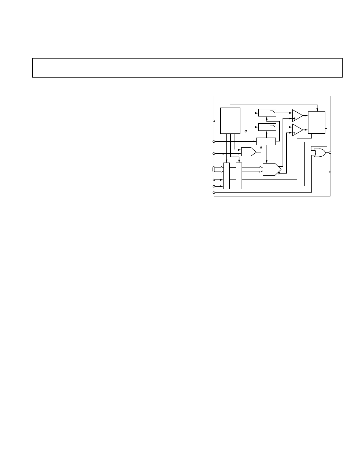
FUNCTIONAL BLOCK DIAGRAM
Additionally, input data setup and hold time are symmetrical at
2 ns each, simplifying interface to the system bus.
Finally, chip design and pinout are optimized to decrease
sensitivity of analog circuits to digital coupling. (See layout
section for detailed recommendations for optimum results.)
Inputs are TTL or CMOS compatible, and outputs are CMOS
compatible. The AD9561JR is packaged in a 28-lead plastic
SOIC. It is rated over the commercial temperature range, 0°C
to +70°C.
HIGHLIGHTS
1. 60 MHz native printer clock rate.
2. Single +5 V power supply.
3. On-chip Autocalibration.
4. Pulse placement flexibility.
5. High resolution: 256 pulse widths.
REV. 0
Information furnished by Analog Devices is believed to be accurate and
reliable. However, no responsibility is assumed by Analog Devices for its
use, nor for any infringements of patents or other rights of third parties
which may result from its use. No license is granted by implication or
otherwise under any patent or patent rights of Analog Devices.
One Technology Way, P.O. Box 9106, Norwood, MA 02062-9106, U.S.A.
Tel: 617/329-4700 World Wide Web Site: http://www.analog.com
Fax: 617/326-8703 © Analog Devices, Inc., 1996
Page 2

AD9561–SPECIFICATIONS
(+VS = +5 V; R
= 715 V, CLOCK = 20 MHz unless otherwise noted)
SET
AD9561JR
Parameter Temp Min Typ Max Units
RESOLUTION 8 Bits
ACCURACY (@ 20 MHz)
Differential Nonlinearity +25°C ±0.5 ±2 LSB
Integral Linearity
Odd/Even Pulse Mismatch
1
2
+25°C ± 1.5 ±4 LSB
+25°C ±0.75 LSB
DIGITAL INPUTS
Logic “1” Voltage Full 2.0 V
Logic “0” Voltage Full 0.8 V
Input Current Full ±1 µA
Input Capacitance
+25°C
5pF
Data Setup Time Full 2.0 0.3 ns
Data Hold Time Full 2.0 0.3 ns
Minimum Clock Pulse Width (HIGH) Full 6 ns
DYNAMIC PERFORMANCE
Maximum Trigger Rate Full 60 MHz
Minimum Propagation Delay (t
Minimum Propagation Delay TC Full 60 ps/°C
Output Pulse Width @ Code 25
Output Pulse Width @ Code 255 Full 100 % Clock
Output Rise Time
Output Fall Time
5, 6
5, 6
PD
3
)
4
+25°C122028ns
Full 5 ns
Full 1.8 3 ns
Full 1.8 3 ns
RETRACE Propagation Delay Full 6 ns
PWM OUTPUT
Logic “1” Voltage
Logic “0” Voltage
5, 6
5, 6
Full 4.6 V
Full 0.4 V
CAL OUT
Logic “1” Voltage Full 4.6 V
Logic “0” Voltage Full 0.4 V
POWER SUPPLY
7
Positive Supply Current (+5.0 V) Full 140 170 mA
Power Dissipation Full 700 850 mW
Power Reduce Current Full 70 85 mA
Power Reduce Dissipation Full 350 425 mW
Power Supply Rejection Ratio
Propagation Delay Sensitivity (TEM)
NOTES
1
Best Fit between codes 25 and 230. INL is very layout sensitive.
2
Due to linearity mismatch in dual ramps.
3
Measured from rising edge of clock to transition of Codes 0 to 255.
4
Minimum pulse width (at 20 MHz) limited by rise time. Pulse width for Code 25 will be greater when CLOCK < 20 MHz.
5
Output load = 10 pF and 2 mA source/sink.
6
Load conditions to test output drive capability. Linearity will degrade with either capacitive or current loading. Best linearity obtained driving a single CMOS input.
7
All performance specifications valid when supply maintained at +5 V, ±5%.
8
Tested from +4.75 V to +5.25 V.
Specification subject to change without notice.
8
+25°C 1.5 ns/V
–2–
REV. 0
Page 3
AD9561
28
27
26
22
21
20
19
18
17
25
24
23
TOP VIEW
(Not to Scale)
1
2
3
7
8
9
10
11
12
4
5
6
13
14
16
15
AD9561
OUT
V
DD
D2
D1
GND
V
DD
RETRACE
CAL START
V
DD
GND
D0 (LSB)
LEM/TEM
SEM/DEM
GND
D3
D4
D5
V
DD
GND
V
DD
CAL OUT
GND
D7(MSB)
CLOCK
GND
R
SET
D6
PWR REDUCE
WARNING!
ESD SENSITIVE DEVICE
ABSOLUTE MAXIMUM RATINGS
1
PIN CONFIGURATION
Positive Supply Voltage . . . . . . . . . . . . . . . . . . . . . . . . . . +7 V
Digital Input Voltage Range . . . . . . . . . . . . . . . –0.5 V to V
Minimum R
Digital Output Current (Sourcing)
Digital Output Current (Sinking)
Operating Temperature Range
. . . . . . . . . . . . . . . . . . . . . . . . . . . . . . . 120 Ω
SET
2
. . . . . . . . . . . . . . . 10 mA
2
. . . . . . . . . . . . . . . . 10 mA
3
. . . . . . . . . . . . . 0°C to +70°C
DD
Storage Temperature Range . . . . . . . . . . . . –65°C to +150°C
Junction Temperature . . . . . . . . . . . . . . . . . . . . . . . . .+150°C
Lead Soldering Temperature (10 sec)
NOTES
1
Absolute maximum ratings are limiting values, to be applied individually, and
beyond which serviceability may be impaired. Functional operation under any of
these conditions is not necessarily implied.
2
CAL OUT should drive a single TTL or CMOS input.
3
Typical Thermal Impedance:
28-lead SOIC (plastic) θJA = 71.4 °C/W; θJC = 23°C/W.
4
When soldering surface mount packages in vapor phase equipment, temperature
should not exceed 220°C for more than one minute.
4
. . . . . . . . . . . .+300°C
ORDERING GUIDE
Temperature Package Package
PIN DESCRIPTIONS
Model Range Description Option
Pin Name Description
AD9561JR 0°C to +70°C 28-Lead SOIC R-28
AD9561JR-REEL* 0°C to +70°C 28-Lead SOIC R-28
*Tape and Reel ordered in multiples of 1000 ICs.
1–5 D3–D7 Digital Data Bits, D7 Is MSB
6 CLOCK Clock Input
7V
DD
8 GND Ground Return
9V
DD
10 GND Ground Return
11 CAL OUT Calibration Complete Output
12
POWER REDUCE Place AD9561 in Sleep Mode
13 GND Ground Return
14 R
SET
15 GND Ground Return
16 V
DD
17 CAL START Initiates Calibration Cycle
18 RETRACE Force Output High
19 V
DD
20 GND Ground Return
21 OUT Modulated Pulse Out
22 GND Ground Return
CAUTION
ESD (electrostatic discharge) sensitive device. Electrostatic charges as high as 4000 V readily
accumulate on the human body and test equipment and can discharge without detection.
Although the AD9561 features proprietary ESD protection circuitry, permanent damage may
occur on devices subjected to high energy electrostatic discharges. Therefore, proper ESD
precautions are recommended to avoid performance degradation or loss of functionality.
REV. 0
23 V
DD
24 LEM/TEM Controls Leading (1) or
25 SEM/DEM Controls Single (1) or Dual (0)
26–28 D0–D2 Digital Data Bits, D0 is LSB
–3–
+5 V Supply
+5 V Supply
Ramp Current Set Resistor
+5 V Supply
+5 V Supply
+5 V Supply
Trailing (0) Edge Modulation
Edge Modulation
Page 4

AD9561
LEADING EDGE
MODULATION
TRAILING EDGE
MODULATION
DUAL EDGE
MODULATION
CLOCK
N
N+1 N+1
THEORY OF OPERATION
General
The AD9561 is a mixed signal IC designed to provide highspeed pulse width modulation in laser printers and copiers. It
uses high performance analog circuits to achieve high resolution
pulse control without requiring the excessively high clock rates
of an all digital solution.
Because of the sensitivity of analog circuits to digital crosstalk,
PCB layout is critical for achieving optimum results. Please read the
layout section at the end of this data sheet and follow suggestions
completely for best performance.
The AD9561 was designed to facilitate either higher effective
resolution or photo-realistic image reproduction on low cost
laser print platforms. Its 8-bit pulse width resolution and pulse
positioning capabilities combine to offer the highest level of gray
shading and resolution enhancement flexibility available. It
also includes an autocalibration circuit to minimize external
components, and eliminates an extra burden on the system
microprocessor.
The Functional Block Diagram illustrates the analog content,
comprising ramp generators, DACs and comparators that
generate a series of pulses. These pulses are combined in the
output logic to form PWM OUT pulses whose width is proportional to the 8-bit DATA and whose position is determined by
the SEM/DEM and LEM/TEM inputs.
The AD9561 employs a proprietary ramp topology that
eliminates the loss of dynamic range at the ends of the ramp.
The Functional Block Diagram is shown for illustration purposes
only and does not represent the actual implementation.
Modulation Modes
Positioning the width controlled pulses at the beginning, middle
or end of the CLOCK period, as shown in Figure 2, adds
significantly to the flexibility of the AD9561. This is accomplished through control bit SEM/DEM and LEM/TEM. These
acronyms represent Single-Edge Modulation/Dual-Edge
Modulation and Leading-Edge Modulation/Trailing-Edge
Modulation. SEM/DEM and LEM/TEM are collectively
identified as CONTROL.
DATA
CONTROL
OUTPUT
FF, XX
00, XX C0, 10 C0, 0X C0, 0X 80, 0X 40, 0X 00, XX C0, 0X E0, 11 FF, XX
100%
DNC
PULSE N
0%
DNC
PULSE
N+1
75%
TEM
75%
DEM
75%
DEM
50%
DEM
25%
DEM0%DNC
75%
DEM
87%
LEM
Figure 1. Pulse Pattern Example
Figure 2. Modulation Modes
Pulse positioning within the CLOCK period is defined by the
following table:
Table I. Truth Table
SEM/DEM LEM/TEM Alignment
1 1 LEM
1 0 TEM
0 X DEM
Single-Edge Modulation offers two options in which one edge is
modulated while the other remains fixed relative to the CLOCK.
For Leading-Edge Modulation, the rising edge of the pulse is
delayed from the leading edge of the CLOCK proportional to
DATA, and the falling edge remains fixed at the end of the
CLOCK period. This may also be called “right-hand justified.”
Similarly, Trailing-Edge Modulation has the rising edge fixed
on the beginning of the CLOCK period and the falling edge
delayed proportional to DATA. This can be called “left-hand
justified.”
Dual-Edge Modulation is often called “center justified” because
the delay of both edges varies relative to the CLOCK. With
increasing values for DATA, pulse width increases with its
center remaining constant proportional to the CLOCK.
Like DATA, modulation control inputs SEM/DEM, and
LEM/TEM can be updated at the CLOCK rate up to 60 MHz.
–4–
REV. 0
Page 5

AD9561
t
AC
CAL START
CAL OUT
1µs MIN
Pulse Pattern Example
Figure 1 at the top of the previous page illustrates the PWM
OUT of the AD9561 with various DATA and CONTROL
inputs. The DATA format is Binary. In the Pulse Pattern
Example, the Hexadecimal format is used, i.e., FF
represents
H
decimal 255.
The top line shows the CLOCK; the second shows DATA and
CONTROL inputs, which are latched on the rising edge of
CLOCK. The third line shows the resulting pulse.
The AD9561 DATA and CONTROL inputs are double
latched. The OUTPUT pulse labeled “Pulse N” results from
DATA and CONTROL values latched in by the first CLOCK,
illustrating the one CLOCK period timing delay.
The CONTROL value number for pulse one is shown as xx.
This means the value is not important because a 100% pulse
will be output for any CONTROL value for DATA value 255 or
FF
. Likewise, OUTPUT Pulse N is noted as 100% DNC (do
H
not care), also noting that CONTROL value is unimportant.
The fourth DATA/CONTROL value is C0/0X. This indicates
that the level for LEM/TEM is unimportant when SEM/DEM is
logic Level “0”.
Selecting R
SET
Because the AD9561 must provide full range coverage of the
CLOCK pulse period, the ramp time must be matched to the
CLOCK period. All components for the ramp generators, except
R
, are integrated in the AD9561.
SET
, is selected by the user to set the ramp time close to the
R
SET
CLOCK period. The ramps are generated by constant current
sources charging on-chip capacitors.
R
can be chosen in the range from 226 Ω for 60 MHz
SET
operation to 16.5 kΩ for 1 MHz. Because the absolute value of
the on-chip capacitor can vary by ± 20%, the autocalibration
circuit is included to fine tune the matching of the ramp time to
the CLOCK period.
100
where F is the CLOCK frequency in Hz. The resistor value
determined by the equation will generate a current near centerrange of the autocalibration circuit.
Autocalibration
The AD9561 should be calibrated when power is applied to the
system or after a power reduce cycle.
Figure 4. Autocalibration Timing
Autocalibration is initiated by applying a pulse of 1 µs minimum
duration to Pin 17, CAL START. The CLOCK pulse should be
applied continuously during calibration. As Figure 4 shows, the
initial state of CAL OUT is not known.
During the CAL IN pulse, all internal logic is initialized for
calibration and proper synchronization once calibration is
complete; the falling edge of CAL IN initiates the Auto-CAL
cycle.
Auto-CAL is not affected by the code applied to the DATA or
CONTROL inputs. However, to assure that no pulses are
generated during calibration, it is suggested that all digital
inputs be held at Logic “0.”
On the falling edge of CAL IN, the ramp’s slope is set as slow as
possible for the current R
. Figure 4 shows the RAMP slope
SET
increasing as autocalibration adds small incremental currents,
until it crosses the internal REF LO before the end of the
CLOCK period.
RAMP
END OF CLOCK CYCLE
10
CLOCK FREQUENCY – MHz
1
0201
Figure 3. R
SET
Figure 3 shows approximate values for R
R
– kΩ
SET
Values vs. CLOCK Frequency
SET
10
over the operating
frequency range. The following equation should be used to
determine R
REV. 0
SET
:
30.2068 ×10
R =
1.04414
F
9
REF LO
TIME
RAMP
Figure 5. Autocalibration Conceptual
The calibration current is incremented on each 32nd CLOCK
pulse until the full-scale ramp time is equal to the period of the
CLOCK. Cal Complete is detected and CAL OUT goes high
when the ramp crosses REF LO before it is reset by the next
CLOCK. With a maximum of 64 incremental increases, the
maximum autocalibration time, t
equation:
tAC=
where: FC = CLOCK frequency in Hertz
, can be calculated by the
AC
32×64
F
C
–5–
Page 6

AD9561
This yields the maximum time from the trailing edge of CAL IN
to the rising edge of CAL OUT. As an example, the maximum
time required for auto-calibration for a system with clock frequency
of 20 MHz is 102.4 ms plus the width of the CAL IN pulse.
Power Reduce
The POWER REDUCE function permits the user to power
down all nonessential circuits when the printer is not active.
Applying a Logic “0” to POWER REDUCE decreases the
power supply requirement by approximately half.
APPLICATIONS
DATA Timing
Input DATA to the AD9561 is double latched. As a result of the
internal timing, the OUTPUT is delayed more than one clock
period from its corresponding DATA word. Figure 6 illustrates
timing of DATA and CONTROL inputs relative to the CLOCK.
CLOCK
DATA
CONTROL
SETUP
HOLD
Figure 6. DATA and CONTROL Timing
The DATA and CONTROL inputs to the AD9561 are standard master-slave latches. Inputs are latched in on the rising
edge of the CLOCK with 2 ns Set-Up time and 2 ns Hold time.
This is a design improvement over the AD9560 meant to
simplify interfacing the AD9561 to digital processing circuits.
A propagation delay exists between the CLOCK and OUTPUT
pulses. The minimum propagation delay can be observed when
alternating between codes 0 (00
hexadecimal) and 255 (FF
H
H
hexadecimal). This delay is due in part to normal circuit
propagation; the remainder is due to time required to implement the proprietary ramp function. OUTPUT pulse transitions will typically occur 22 ns after the rising edge of CLOCK.
It may vary from 10 ns–35 ns over temperature.
Transfer Function
Output pulse width increases with increasing DATA values. As
the heavy line of Figure 7 shows, the transfer function of the
AD9561 is slightly nonideal.
100
80
60
40
PULSE WIDTH – Percentage
20
An ideal transfer would give 0% (or 0 ns) pulse width for a Code 0.
As the code is incremented in steps of one, the pulse width would
increase by 0.39% until it reached 100% for Code 255.
When operating at high clock rates, several of the most narrow
pulses do not reach valid logic Level “1” because of finite rise
time. For example, at 20 MHz, a 1.95% pulse (code 5 or 05
)
H
would have an expected pulse width of 1 ns. Because the rise
time is typically 1.5 ns, this pulse will not reach a full output
level. Therefore, depending on the clock rate, the lowest set of
codes produces a series of triangle waves increasing in width
and amplitude until a pulse of approximately 3 ns–5 ns reaches
a proper logic level. Thus, the transfer is flat until about
3 ns–5 ns pulse width (number of codes varies as a function of
CLOCK frequency).
Because of the new ramp topology in the AD9561, the transfer
function extends slightly greater than 100% (typically 102%) of
the clock period. This has the effect of creating smooth transitions
at the CLOCK period boundaries instead of the discontinuities
produced by the AD9560.
t
CLOCK
t
PD
(RIGHT JUSTIFIED)
LEM
t
CLOCK
t
CLOCK
TEM
(LEFT JUSTIFIED)
t
CLOCK
DEM
(CENTER JUSTIFIED)
Figure 8. Dot Clock Period Transitions
As shown in Figure 8, a Leading Edge Modulated pulse followed
by a Trailing Edge Modulated pulse will stay high from the rising
edge of the first pulse to the falling edge of the second. This is
due to Code 255 being designed to be typically 102% of the
CLOCK period. (Dashed lines indicate where transitions
would occur if the code for the following or preceding period
were 0.) Likewise, no gap occurs for maximum width Trailing
Edge Modulation to max pulse width for Dual Edge Modulation. Because the ending and starting characteristics of all
modes are symmetrical, any combination of pulses that ends at
the boundary of the first period and starts at the boundary of
the second period will produce a continuous pulse across the
boundary.
For the purposes of printing text, or any time absolute white or
black is required, 0 is decoded and a 100% LOW is output in
the next CLOCK cycle. Similarly, 255 is detected and the next
pulse is 100% HIGH.
Retrace
The RETRACE function permits driving the output to a
constant Logic High. For laser printer applications, applying a
logic “1” to RETRACE holds the laser on during the retrace
period so end of scan can be detected. Returning it to Logic
Low gives control back to the input data bits D0–D7.
0
025
12.5
128
CODE
255
Figure 7. Pulse Width Transfer Function
–6–
REV. 0
Page 7

AD9561
Grounding and Bypassing
Because the AD9561 uses analog circuits to achieve its superb
gray scale resolution, caution must be exercised when incorporating it into the mostly digital controller card for a printer.
Achieving the accuracy designed into the AD9561 requires that
interference due to improper grounding, power supply noise and
digital coupling be minimized by following good layout practices.
It is strongly urged that all following recommendations be
followed.
Factory characterization proves that a single ground plane
dedicated to the AD9561 is most effective. This is atypical of
many mixed signal circuits that use separate analog and digital
grounds. Due to the operating speed of the AD9561, separate
grounds result in erratic performance, which is eliminated by
using a single isolated ground plane. This is because the DATA
“low” value can be different from the ground value of the
AD9561. All pins on the AD9561 labeled GROUND should
be connected to the single dedicated ground plane. For best
results, it is suggested that this plane be in the first interior layer
under the IC. To assure logic level compatibility from the drive
circuits to the AD9561, a single connection to the board’s main
ground is necessary.
The connection between the dedicated ground plane and the
board’s main ground should be parallel to the path of the digital
signals interfacing to the AD9561. High frequency return current
seeks the path most parallel to the signal current. Whenever a
parallel path does not exist, ground bounce results.
CLOCK, DATA and CONTROL signal traces should run
from the drive logic to the AD9561 in a group parallel to the
connection between the system ground and the AD9561
ground. Using more than one signal plane will permit these
traces to be as close to the ground interconnection as possible.
This results in lowest impedance ground return and minimum
ground interference due to digital switching.
Attention to subtle layout characteristics can yield significant
improvement in performance of high speed mixed signal ICs.
The AD9561 pinouts were chosen for maximum isolation of
sensitive pins such as R
. The Pin 1 end of the IC should be
SET
oriented toward the source of the high speed digital inputs.
This will help assure that these signal runs are short, with
essentially the same length, thus having equal propagation
delays. Most importantly, it will facilitate orienting traces to
minimize coupling.
High speed digital traces including DATA, CLOCK, SEM/
DEM, LEM/TEM and the OUTPUT should not pass under the
body of the IC. The CLOCK, in particular, should enter
perpendicular to the IC.
For best results, the OUTPUT trace should exit perpendicular
to the IC and pass through a via to a signal layer under the
ground plane. This trace or any resistor or other component
of the output circuit should not be parallel to R
as electro-
SET
magnetic coupling can occur, causing the ramp current reference
to be noisy and linearity to deteriorate.
Optimally, R
should be a chip resistor located on the same
SET
side of the board as the AD9561. It should be located close to
Pin 14, without being close to the other IC pins. R
SET
should
be on the top of the board with the AD9561 with no vias to add
stray reactance and additional coupling paths.
To reiterate the key layout considerations, high speed
digital traces should not be located near the R
SET
pin or
under the center of the IC body.
A final interface consideration relates to rise/fall time of
the high speed signals. Some logic families have rise and
fall times as fast as 2 V/ns. This can result in on-chip
parasitic coupling of these signals into the analog section.
The undesirable effect can be eliminated by inserting
series resistors in the DATA, SEM/DEM and LEM/
TEM connections. These resistors, in conjunction with the
capacitance of the input pin and bond pad, will form a low
pass filter to limit slew rate of the signals. The value of
these resistors should be chosen based on trading off slower
rise and fall time to possible interference to set up and hold
times for faster clock rates.
Power supply noise can also disrupt the linear circuits of
the AD9561. Since switching power supplies are becoming
the norm in most systems, caution should be exercised to
minimize switching noise reaching the AD9561. The IC is
designed for maximum power supply rejection. However,
frequency content of switching supply noise often exceeds
the frequency range of highest rejection. The preferred
method would be to use a linear regulator from a higher
supply voltage. If this is not practical, insert a ferrite bead
in series with the supply connection. If possible, a V
DD
plane or a substantial width trace should connect VDD to
Pin 7 first and then connect to each of the other V
DD
pins
with wide traces. Thorough decoupling will complete a low
pass filter for the supply.
All V
connections should be connected together. 0.1 µF
DD
chip capacitors should be connected as closely as possible
to each V
pin to the dedicated ground plane. Laboratory
DD
results indicate that performance is maximized when these
chip capacitors are mounted on the same side of the PC
card as the AD9561. If mounting chip components on the
same side as the AD9561 is not a preferred manufacturing
method, due consideration is encouraged to make an exception, at least in the case of R
and as many decoupling
SET
capacitors as practical. Additionally, a 10 µF tantalum
capacitor should decouple the supply on the AD9561 side
of the regulator or ferrite bead, also to the dedicated
ground plane.
For a recommended layout, see the AD9561/PCB data
sheet. A copy can be obtained by calling Applications
Support at 1-800-ANALOGD.
REV. 0
–7–
Page 8

AD9561
OUTLINE DIMENSIONS
Dimensions shown in inches and (mm).
28-Lead SOIC
(R-28)
0.7125 (18.10)
0.6969 (17.70)
28 15
141
0.2992 (7.60)
0.2914 (7.40)
0.4193 (10.65)
0.3937 (10.00)
C2938–6–12/96
0.0118 (0.30)
0.0040 (0.10)
PIN 1
0.0500
(1.27)
BSC
0.0192 (0.49)
0.0138 (0.35)
0.1043 (2.65)
0.0926 (2.35)
SEATING
PLANE
0.0125 (0.32)
0.0091 (0.23)
0.0291 (0.74)
0.0098 (0.25)
0.0500 (1.27)
8°
0°
0.0157 (0.40)
x 45°
–8–
PRINTED IN U.S.A.
REV. 0
 Loading...