

Page 1
T
655 MHz Low Jitter Clock Generator
FEATURES
Excellent intrinsic jitter performance
25 Mb/s write-speed serial I/O control
200 MHz phase frequency detector inputs
655 MHz programmable input dividers for the phase fre-
quency detector (÷M, ÷N) {M, N = 1..16} (bypassable)
Programmable RF divider (÷R) {R = 1, 2, 4, 8} (bypassable)
8 programmable internal clock rates
Programmable edge delay with 93 f
1.8 V supply for device operation
3.3 V supply for I/O, CML driver, and charge pump output
Software controlled power-down
48-lead LFCSP package
Programmable charge pump current (up to 4 mA)
Multichip synchronization
Dual-mode PLL lock detect
655 MHz CML-mode PECL-compliant driver
SYNC_IN/STATUS
resolution
S
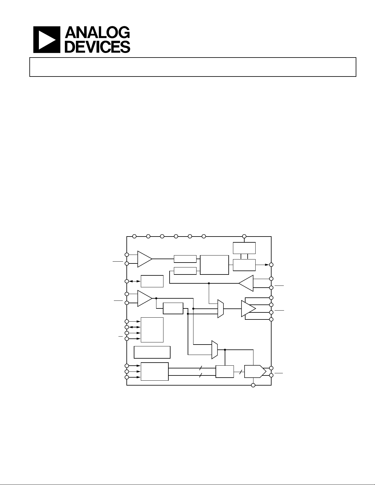
FUNCTIONAL BLOCK DIAGRAM
AVDD AGND DVDD DGND VCML VCP CP_RSET
REFIN
REFIN
SYNC, PLL
LOCK
CLK1
CLK1
SCLK
SDI/O
SDO
CS
SERIAL
CONTROL
PORT
TIMING AND
CONTROL LOGIC
DIVIDER
1, 2, 4, 8
M DIVIDER
N DIVIDER
APPLICATIONS
Clocking high performance data converters
Base station clocking applications
Network (SONET/SDH) clocking
Gigabit Ethernet (GbE) clocking
Instrumentation clocking circuits
CP
REF, AMP
FREQUENCY
DETECTOR
CLK
DIVCLK
PHASE
CHARGE
PUMP
CML
CP
CLK2
CLK2
DRV_RSE
OUT0
OUT0
VCML
AD9540
S2
S1
S0
FREQUENCY
PROFILES
Rev. 0
Information furnished by Analog Devices is believed to be accurate and reliable.
However, no responsibility is assumed by Analog Devices for its use, nor for any
infringements of patents or other rights of third parties that may result from its use.
Specifications subject to change without notice. No license is granted by implication
or otherwise under any patent or patent rights of Analog Devices. Trademarks and
registered trademarks are the property of their respective owners.
PHASE/
48
14
Figure 1.
10
DDS
One Technology Way, P.O. Box 9106, Norwood, MA 02062-9106, U.S.A.
Tel: 781.329.4700
Fax: 781.326.8703 © 2004 Analog Devices, Inc. All rights reserved.
DAC
DAC_RSET
www.analog.com
IOUT
IOUT
04947-001
Page 2

AD9540
TABLE OF CONTENTS
Product Overview............................................................................. 3
DDS and DAC ............................................................................ 20
Specifications..................................................................................... 4
Loop Measurement Conditions.................................................. 9
Absolute Maximum Ratings.......................................................... 10
ESD Caution................................................................................ 10
Pin Configuration and Function Descriptions........................... 11
Typical Performance Characteristics ...........................................13
Typical Application Circuits.......................................................... 18
Application Circuit Descriptions ............................................. 18
General Description ....................................................................... 19
PLL Circuitry .............................................................................. 19
CML Driver................................................................................. 19
REVISION HISTORY
7/04—Revision 0: Initial Version
Modes of Operation ....................................................................... 21
Selectable Clock Frequencies and Selectable Edge Delay ..... 21
Synchronization Modes for Multiple Devices.............................. 21
Serial Port Operation ..................................................................... 22
Instruction Byte.......................................................................... 23
Serial Interface Port Pin Description....................................... 23
MSB/LSB Transfers .................................................................... 23
Register Map and Description...................................................... 24
Control Function Register Descriptions................................. 27
Outline Dimensions....................................................................... 32
Ordering Guide .......................................................................... 32
Rev. 0 | Page 2 of 32
Page 3

AD9540
PRODUCT OVERVIEW
The AD9540 is Analog Devices’ first dedicated clocking product
specifically designed to support the extremely stringent clocking requirements of the highest performance data converters.
The device features high performance PLL circuitry, including a
flexible 200 MHz phase frequency detector and a digitally
controlled charge pump current. The device also provides a low
jitter, 655 MHz CML-mode, PECL-compliant output driver with
programmable slew rates. External VCO rates up to 2.7 GHz are
supported. Extremely fine tuning resolution (steps less than
2.33 µHz) is another feature supported by this device. Information is loaded into the AD9540 via a serial I/O port that has a
device write-speed of 25 Mb/s. The AD9540 frequency
divider block can also be programmed to support a spread
spectrum mode of operation.
The AD9540 is specified to operate over the extended
automotive range of −40°C to +85°C.
Rev. 0 | Page 3 of 32
Page 4

AD9540
SPECIFICATIONS
AVDD = DVDD = 1.8 V ± 5%; DVDD_I/O = CP_VDD = 3.3 V ± 5% (@ TA = 25°C), DAC_R
DRV_R
= 4.02 kΩ, unless otherwise noted.
SET
Table 1.
Parameter Min Typ Max Unit Test Conditions/Comments
TOTAL SYSTEM JITTER AND PHASE NOISE FOR
105 MHz ADC CLOCK GENERATION CIRCUIT
Converter Limiting Jitter1 720 fS rms
Resultant SNR 59.07 dB
Phase Noise of Fundamental
@ 10 Hz Offset 80 dBc/Hz
@ 100 Hz Offset 92 dBc/Hz
@ 1 kHz Offset 101 dBc/Hz
@ 10 kHz Offset 110 dBc/Hz
@ 100 kHz Offset 147 dBc/Hz
≥1 MHz Offset 153 dBc/Hz
TOTAL SYSTEM PHASE NOISE FOR 210 MHz
ADC CLOCK GENERATION CIRCUIT
Phase Noise of Fundamental
@ 10 Hz Offset 79.2 dBc/Hz
@ 100 Hz Offset 86 dBc/Hz
@ 1 kHz Offset 95 dBc/Hz
@ 10 kHz Offset 105 dBc/Hz
@ 100 kHz Offset 144 dBc/Hz
@ 1 MHz Offset 151 dBc/Hz
TOTAL SYSTEM TIME JITTER FOR CLOCKS
155.52 MHz Clock 581 fS rms 12 kHz to 1.3 MHz bandwidth
622.08 MHz Clock 188 fS rms 12 kHz to 5 MHz bandwidth
RF DIVIDER/CML DRIVER EQUIVALENT
INTRINSIC TIME JITTER
FIN = 414.72 MHz, F
FIN = 1244.16 MHz, F
FIN = 2488.32 MHz, F
= 51.84 MHz 136 fS rms R = 8, BW = 12 kHz to 400 kHz
OUT
= 155.52 MHz 101 fS rms R = 8, BW = 12 kHz to 1.3 MHz
OUT
= 622.08 MHz 108 fS rms R = 4, BW = 12 kHz to 5 MHz
OUT
RF DIVIDER/CML DRIVER RESIDUAL PHASE NOISE
FIN = 81.92 MHz, F
= 10.24 MHz RF Divider R = 8
OUT
@ 10 Hz 120 dBc/Hz
@ 100 Hz 128 dBc/Hz
@ 1 kHz 137 dBc/Hz
@ 10 kHz 145 dBc/Hz
@ 100 kHz 150 dBc/Hz
≥1 MHz 153 dBc/Hz
FIN = 983.04 MHz, F
= 122.88 MHz RF Divider R = 8
OUT
@ 10 Hz 115 dBc/Hz
@ 100 Hz 125 dBc/Hz
@ 1 KHz 132 dBc/Hz
@ 10 kHz 142 dBc/Hz
@ 100 kHz 146 dBc/Hz
@ 1 MHz 151 dBc/Hz
>3 MHz 153 dBc/Hz
= 3.92 kΩ, CP_R
SET
= 3.09 kΩ,
SET
Rev. 0 | Page 4 of 32
Page 5

AD9540
Parameter Min Typ Max Unit Test Conditions/Comments
FIN = 1966.08 MHz, F
@ 10 Hz 105 dBc/Hz
@ 100 Hz 112 dBc/Hz
@ 1 kHz 122 dBc/Hz
@ 10 kHz 130 dBc/Hz
@ 100 kHz 141 dBc/Hz
@ 1 MHz 144 dBc/Hz
>3 MHz 146 dBc/Hz
FIN = 2488 MHz, F
@ 10 Hz 100 dBc/Hz
@ 100 Hz 108 dBc/Hz
@ 1 kHz 115 dBc/Hz
@ 10 kHz 125 dBc/Hz
@ 100 kHz 135 dBc/Hz
@ 1 MHz 140 dBc/Hz
≥3 MHz 142 dBc/Hz
PHASE FREQUENCY DETECTOR/CHARGE PUMP
REFIN Input
Input Frequency2
÷M Set to Divide by at Least 4 655 MHz
÷M Bypassed 200 MHz
Input Voltage Levels 200 450 600 mV p-p
Input Capacitance 10 pF
Input Resistance 1500 Ω
CLK2 Input
Input Frequency
÷N Set to Divide by at Least 4 655 MHz
÷N Bypassed 200 MHz
Input Voltage Levels 200 450 600 mV p-p
Input Capacitance 10 pF
Input Resistance 1500 Ω
Charge Pump Source/Sink Maximum Current 4 mA
Charge Pump Source/Sink Accuracy 5 %
Charge Pump Source/Sink Matching 2 %
Charge Pump Output Compliance Range3 0.5 CPVDD − 0.5 V
STATUS Drive Strength 2 mA
PHASE FREQUENCY DETECTOR NOISE FLOOR
@ 50 kHz PFD Frequency 148 dBc/Hz
@ 2 MHz PFD Frequency 133 dBc/Hz
@ 100 MHz PFD Frequency 116 dBc/Hz
@ 200 MHz PFD Frequency 113 dBc/Hz
RF DIVIDER (CLK1 ) INPUT SECTION (÷R)
RF Divider Input Range 1 2700 MHz
Input Capacitance (DC) 3 pF
Input Impedance (DC) 1500 Ω
Input Duty Cycle 42 50 58 %
Input Power/Sensitivity −10 +4 dBm Single-ended, into a 50 Ω load4
Input Voltage Level 200 1000 mV p-p
= 491.52 MHz RF Divider R = 4
OUT
= 622 MHz RF Divider R = 4
OUT
DDS SYSCLK not to
exceed 400 MSPS
Rev. 0 | Page 5 of 32
Page 6

AD9540
Parameter Min Typ Max Unit Test Conditions/Comments
CML OUTPUT DRIVER (OUT0)
Differential Output Voltage Swing5 720 mV 50 Ω load to supply, both lines
Maximum Toggle Rate 655
Common-Mode Output Voltage 1.75 V
Output Duty Cycle 42 58 %
Output Current
Continuous6 7.2 mA
Rising Edge Surge 20.9 mA
Falling Edge Surge 13.5 mA
Output Rise Time 250 ps 100 Ω terminated, 5 pF load
Output Fall Time 250 ps 100 Ω terminated, 5 pF load
LOGIC INPUTS (SDI/O, I/O_RESET, RESET,
I/O_UPDATE, S0, S1, S2, SYNC_IN)
7
VIH, Input High Voltage 2.0 V
VIL, Input Low Voltage 0.8 V
I
, I
, Input Current ±1 ±5 µA
INH
INL
CIN, Maximum Input Capacitance 3 pF
LOGIC OUTPUTS (SDO, SYNC_OUT, STATUS)8
VOH, Output High Voltage 2.7 V
VOH, Output Low Voltage 0.4 V
IOH 100 µA
IOL 100 µA
POWER CONSUMPTION
Total Power Consumed, All Functions On 400 mW
IAVDD 85 mA
IDVDD 45 mA
IDVDD_I/O 20 mA
ICPVDD 15 mA
Power-Down Mode 80 mW
WAKE-UP TIME (FROM POWER-DOWN MODE)
Digital Power-Down (CFR1<7>) 12 ns
DAC Power-Down (CFR2<39>) 7 µs
RF Divider Power-Down (CFR2<23>) 400 ns
Clock Driver Power-Down (CFR2<20>) 6 µs
Charge Pump Full Power-Down (CFR2<4>) 10 µs
Charge Pump Quick Power-Down (CFR2<3>) 150 ns
CRYSTAL OSCILLATOR (ON REFIN INPUT)
Operating Range 20 25 30 MHz
Residual Phase Noise (@ 25 MHz)
@ 10 Hz Offset 95 dBc/Hz
@ 100 Hz Offset 120 dBc/Hz
@ 1 kHz Offset 140 dBc/Hz
@ 10 kHz Offset 157 dBc/Hz
@ 100 kHz Offset 164 dBc/Hz
>1 MHz Offset 168 dBc/Hz
DIGITAL TIMING SPECIFICATIONS
CS
to SCLK Setup Time TPRE
Period of SCLK (Write) TSCLKW 40 ns
Period of SCLK (Read) TSCLKR 400 ns
Serial Data Setup Time TDSU 6.5 ns
Serial Data Hold Time TDHD 0 ns
Data Valid Time TDV 40 ns
6 ns
Rev. 0 | Page 6 of 32
Page 7
AD9540
Parameter Min Typ Max Unit Test Conditions/Comments
I/O Update to SYNC_CLK Setup Time 7 ns
PS<2:0> to SYNC_CLK Setup Time 7 ns
Latencies/Pipeline Delays
I/O Update to DAC Frequency Change 33 SYSCLK Cycles
I/O Update to DAC Phase Change 33 SYSCLK Cycles
PS<2:0> to DAC Frequency Change 29 SYSCLK Cycles
PS<2:0> to DAC Phase Change 29 SYSCLK Cycles
I/O Update to CP_OUT Scaler Change 4 SYSCLK Cycles
I/O Update to Frequency Accumulator
Step Size Change
DAC OUTPUT CHARACTERISTICS
Resolution 10 Bits
Full-Scale Output Current 10 15 mA
Gain Error −10 +10 % FS
Output Offset 0.6 µA
Output Capacitance 5 pF
Voltage Compliance Range AVDD − 0.50 AVDD + 0.50
Wideband SFDR (DC to Nyquist)
10 MHz Analog Out 65 dBc
40 MHz Analog Out 62 dBc
80 MHz Analog Out 57 dBc
120 MHz Analog Out 56 dBc
160 MHz Analog Out 54 dBc
Narrow-Band SFDR
10 MHz Analog Out (±1 MHz) 83 dBc
10 MHz Analog Out (±250 kHz) 85 dBc
10 MHz Analog Out (±50 kHz) 86 dBc
40 MHz Analog Out (±1 MHz) 82 dBc
40 MHz Analog Out (±250 kHz) 84 dBc
40 MHz Analog Out (±50 kHz) 87 dBc
80 MHz Analog Out (±1 MHz) 80 dBc
80 MHz Analog Out (±250 kHz) 82 dBc
80 MHz Analog Out (±50 kHz) 86 dBc
120 MHz Analog Out (±1 MHz) 80 dBc
120 MHz Analog Out (±250 kHz) 82 dBc
120 MHz Analog Out (±50 kHz) 84 dBc
160 MHz Analog Out (±1 MHz) 80 dBc
160 MHz Analog Out (±250 kHz) 82 dBc
160 MHz Analog Out (±50 kHz) 84 dBc
DAC RESIDUAL PHASE NOISE
19.7 MHz F
@ 10 Hz Offset 122 dBc/Hz
@ 100 Hz Offset 134 dBc/Hz
@ 1 kHz Offset 143 dBc/Hz
@ 10 kHz Offset 150 dBc/Hz
@ 100 kHz Offset 158 dBc/Hz
>1 MHz Offset 160 dBc/Hz
OUT
4 SYSCLK Cycles
Rev. 0 | Page 7 of 32
Page 8

AD9540
Parameter Min Typ Max Unit Test Conditions/Comments
51.84 MHz F
@ 10 Hz Offset 110 dBc/Hz
@ 100 Hz Offset 121 dBc/Hz
@ 1 kHz Offset 135 dBc/Hz
@ 10 kHz Offset 142 dBc/Hz
@ 100 kHz Offset 148 dBc/Hz
> 1 MHz Offset 153 dBc/Hz
105 MHz Analog Out
@ 10 Hz Offset 105 dBc/Hz
@ 100 Hz Offset 115 dBc/Hz
@ 1 kHz Offset 126 dBc/Hz
@ 10 kHz Offset 132 dBc/Hz
@ 100 kHz Offset 140 dBc/Hz
>1 MHz Offset 145 dBc/Hz
155.52 MHz Analog Out
@ 10 Hz Offset 100 dBc/Hz
@ 100 Hz Offset 112 dBc/Hz
@ 1 kHz Offset 123 dBc/Hz
@ 10 kHz Offset 131 dBc/Hz
@ 100 kHz Offset 138 dBc/Hz
>1 MHz Offset 144 dBc/Hz
OUT
1
The SNR of a 14-bit ADC was measured with an ENCODE rate of 105 MSPS and an AIN of 170 MHz. The resultant SNR was known to be limited by the jitter of the clock,
not by the noise on the AIN signal. From this SNR value, the jitter affecting the measurement can be back calculated.
2
Driving the PLLREF input buffer. The crystal oscillator section of this input stage performs up to only 30 MHz.
3
The charge pump output compliance range is functionally 0.2 V to (CPVDD − 0.2 V). The value listed here is the compliance range for 5% matching.
4
The input impedance of the CLK1 input is 1500 Ω. However, to provide matching on the clock line, an external 50 Ω load is used.
5
Measured as peak-to-peak between DAC outputs.
6
For a 4.02 kΩ resistor from DRV_RSET to GND.
7
IBIS models for the digital I/O pins available upon request.
8
Assumes a 1 mA load.
Rev. 0 | Page 8 of 32
Page 9
AD9540
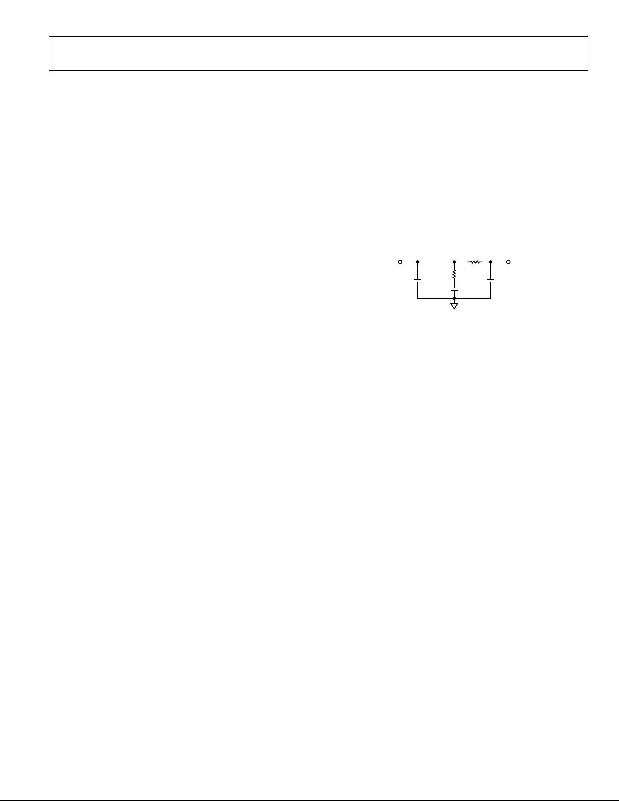
LOOP MEASUREMENT CONDITIONS
622 MHz OC-12 Clock
VCO = Sirenza 190-640T
105 MHz Converter Clock
VCO = Sirenza 190-845T
Reference = Wenzel 500-10116 (30.3 MHz)
Loop Filter = 10 kHz BW, 60° Phase Margin
C1 = 170 nF, R1 = 14.4 Ω, C2 = 5.11 µF, R2 = 89.3 Ω,
C3 Omitted
CP_OUT = 4 mA (Scaler = ×8)
÷R = 2, ÷M = 1, ÷N = 1
Reference = Wenzel 500-10116 (30.3 MHz)
Loop Filter = 10 kHz BW, 45° Phase Margin
C1 = 117 nF, R1 = 28 Ω, C2 = 1.6 µF, R2 = 57.1 Ω, C3 = 53.4 nF
CP_OUT = 4 mA (Scaler = ×8)
÷R = 8, ÷M = 1, ÷N = 1
INPUT OUTPUT
C1
Figure 2. Generic Loop Filter
R2
R1
C2
C3
04806-0-033
Rev. 0 | Page 9 of 32
Page 10

AD9540
ABSOLUTE MAXIMUM RATINGS
Table 2.
Parameter Rating
Analog Supply Voltage (AVDD) 2 V
Digital Supply Voltage (DVDD) 2 V
Digital I/O Supply Voltage
(DVDD_I/0)
Charge Pump Supply Voltage
(CPVDD)
Maximum Digital Input Voltage −0.5 V to DVDD_I/O + 0.5 V
Storage Temperature −65°C to +150°C
Operating Temperature Range −40°C to +125°C
Lead Temperature Range
(Soldering 10 sec)
Junction Temperature 150°C
Thermal Resistance (θJA) 26°C/W
Stresses above those listed under Absolute Maximum Ratings
may cause permanent damage to the device. This is a stress
rating only; functional operation of the device at these or any
other condition s above those indicated in the operational
section of this specification is not implied. Exposure to absolute
maximum rating conditions for extended periods may affect
device reliability.
3.6 V
3.6 V
300°C
ESD CAUTION
ESD (electrostatic discharge) sensitive device. Electrostatic charges as high as 4000 V readily accumulate on the
human body and test equipment and can discharge without detection. Although this product features proprietary ESD protection circuitry, permanent damage may occur on devices subjected to high energy electrostatic
discharges. Therefore, proper ESD precautions are recommended to avoid performance degradation or loss of
functionality.
Rev. 0 | Page 10 of 32
Page 11

AD9540
PIN CONFIGURATION AND FUNCTION DESCRIPTIONS
AVDD
DAC_RSET
DRV_RSET
CP_RSET
AVDD
AGND
CLK2
CLK2
REFIN
REFIN
AVDD
AGND
DGND
36
35
34
33
32
31
30
29
28
27
26
25
CP
VCP
AGND
OUT0
OUT0
VCML
AGND
CLK1
CLK1
AVDD
AGND
DVDD
04947-002
AGND
AVDD
AGND
AVDD
IOUT
IOUT
AVDD
AGND
I/O_RESET
RESET
DVDD
DGND
43 42 41 40 39 38 3748 47 46 45 44
1
PIN 1
INDICATOR
2
3
4
5
6
7
8
9
10
11
12
14
13 15 16 17 18 19 20 21 22 23 24
SDO
SDI/O
SCLK
AD9540
TOP VIEW
(Not to Scale)
CS
DVDD_I/O
SYNC_OUT
I/O_UPDATE
SYNC_IN/STATUS
Figure 3. 48-Lead LFCSP Pin Configuration
S0S1S2
NOTE: The exposed paddle on this package is an electrical connection (Pin 49) as well as a thermal enhancement. For the device to
function properly, the paddle must be attached to analog ground.
Rev. 0 | Page 11 of 32
Page 12

AD9540
Table 3. 48-Lead LFCSP Pin Function Descriptions
Pin No. Mnemonic Description
1, 3, 8, 26, 30,
34, 37, 43, 49
2, 4, 7, 27, 38,
44, 48
5 IOUT DAC Analog Output.
6
9 I/O_RESET
10 RESET Master RESET. Clears all accumulators and returns all registers to their default values (active high).
11, 25 DVDD Digital Core Supply (1.8 V).
12, 24 DGND Digital Ground.
13 SDO Serial Data Output. Used only when device is programmed for 3-wire serial data mode.
14 SDI/O
15 SCLK Serial Data Clock. Provides the clock signal for the serial data port.
16
17 DVDD_I/O Digital Interface Supply (3.3 V).
18 SYNC_OUT Synchronization Clock Output.
19 SYNC_IN/STATUS
20 I/O_UPDATE
21, 22, 23 S0, S1, S2 Clock Frequency and Delay Select Pins. Specify one of eight clock frequency/delay profiles.
28
29 CLK1 RF Divider and Internal Clock Input.
31 VCML CML Driver Supply Pin.
32
33 OUT0 CML Driver Output.
35 VCP
36 CP Charge Pump Output.
39 REFIN Phase Frequency Detector Reference Input.
40
41
42 CLK2 Phase Frequency Detector Oscillator (Feedback) Input.
45 CP_RSET Charge Pump Current Set (Program Charge Pump Current with a Resistor to AGND).
46 DRV_RSET CML Driver Output Current Set (Program CML Output Current with a Resistor to AGND).
47 DAC_RSET DAC Output Current Set (Program DAC Output Current with a Resistor to AGND).
AGND Analog Ground.
AVDD Analog Core Supply (1.8 V).
IOUT
CS Active Low Signal That Enables Shared Serial Buses. When brought high, the serial port ignores the
CLK1
OUT0
REFIN
CLK2
DAC Analog Complementary Output.
Resets the serial port when synchronization is lost in communications but does not reset the de-
vice itself (active high). When not being used, this pin should be forced low, because it floats to the
threshold value.
Serial Data I/O. When the part is programmed for 3-wire serial data mode, this is input only; in
2-wire mode, it serves as both the input and output.
serial data clocks.
Bidirectional Dual Function Pin. Depending on device programming, this pin is either the DDS’s
synchronization input (allows alignment of multiple subclocks), or the PLL lock detect output signal.
This input pin, when set high, transfers the data from the I/O buffers to the internal registers on the
rising edge of the internal SYNC_CLK, which can be observed on SYNC_OUT.
RF Divider and Internal Clock Input.
CML Driver Complementary Output.
Charge Pump Supply Pin (3.3 V). To minimize noise on the charge pump, isolate this supply from
DVDD_I/O.
Phase Frequency Detector Reference Complementary Input.
Phase Frequency Detector Oscillator (Feedback) Complementary Input.
NOTE: The exposed paddle on this package is an electrical connection (Pin 49) as well as a thermal enhancement. In order for the device
to function properly, the paddle must be attached to analog ground.
Rev. 0 | Page 12 of 32
Page 13

AD9540
TYPICAL PERFORMANCE CHARACTERISTICS
RF ATT
100Hz
DELTA 1 [T1]
REF LVL
0dBm
0
–10
–20
–30
–40
–50
–60
–70
–80
–90
–100
CENTER 10.1MHz 5kHz/ SPAN 50kHz
–85.94dB
–2.10420842kHz
RBW
100Hz
VBW
25s
SWT
1
1
UNIT
Figure 4. AD9540 DAC Performance: 400 MSPS Clock,
–86.03dB
, 50 kHz Span
OUT
RBW
VBW
SWT
1
500Hz
500Hz
20s
RF ATT
UNIT
10 MHz F
REF LVL
0dBm
0
–10
–20
–30
–40
–50
–60
–70
–80
–90
–100
CENTER 10.1MHz 100kHz/ SPAN 1MHz
DELTA 1 [T1]
–368.73747495kHz
1
Figure 5. AD9540 DAC Performance: 400 MSPS Clock,
–64.54dB
, 1 MHz Span
OUT
RBW
VBW
SWT
1
10kHz
10kHz
5s
RF ATT
UNIT
10 MHz F
REF LVL
0dBm
0
1
–10
–20
–30
–40
–50
–60
–70
–80
–90
–100
START 0Hz 20MHz/ STOP 200MHz
DELTA 1 [T1]
100.20040080MHz
Figure 6. AD9540 DAC Performance: 400 MSPS Clock,
10 MHz F
, 200 MHz Span
OUT
20dB
20dB
20dB
DELTA 1 [T1]
REF LVL
dB
A
1 AP
04947-003
0dBm
0
–10
–20
–30
–40
–50
–60
–70
–80
–90
–100
CENTER 40.1MHz 5kHz/ SPAN 50kHz
–84.94dB
2.10420842kHz
RBW
VBW
SWT
1
1
Figure 7. AD9540 DAC Performance: 400 MSPS Clock,
–80.17dB
, 50 kHz Span
OUT
RBW
VBW
SWT
1
40 MHz F
REF LVL
dB
A
1 AP
04947-004
0dBm
0
–10
–20
–30
–40
–50
–60
–70
–80
–90
–100
CENTER 40.1MHz 100kHz/ SPAN 1MHz
DELTA 1 [T1]
–200.40080160kHz
1
Figure 8. AD9540 DAC Performance: 400 MSPS Clock,
–61.61dB
, 1 MHz Span
OUT
RBW
VBW
SWT
40 MHz F
REF LVL
dB
A
1 AP
04947-005
0dBm
0
–10
–20
–30
–40
–50
–60
–70
–80
–90
–100
START 0Hz 20MHz/ STOP 200MHz
DELTA 1 [T1]
100.20040080MHz
1
Figure 9. AD9540 DAC Performance: 400 MSPS Clock,
40 MHz F
, 200 MHz Span (Nyquist)
OUT
100Hz
100Hz
25s
500Hz
500Hz
20s
10kHz
10kHz
1
RF ATT
20dB
UNIT
dB
A
1 AP
04947-006
RF ATT
20dB
UNIT
dB
A
1 AP
04947-007
RF ATT
20dB
5s
UNIT
dB
A
1 AP
04947-008
Rev. 0 | Page 13 of 32
Page 14

AD9540
REF LVL
0dBm
0
–10
–20
–30
–40
–50
–60
–70
–80
–90
–100
CENTER 100.1MHz 5kHz/ SPAN 50kHz
Figure 10. AD9540 DAC Performance: 400 MSPS Clock,
REF LVL
0dBm
0
–10
–20
–30
–40
–50
–60
–70
–80
–90
–100
CENTER 100.1MHz 100kHz/ SPAN 1kHz
Figure 11. AD9540 DAC Performance: 400 MSPS Clock,
REF LVL
0dBm
0
–10
–20
–30
–40
–50
–60
–70
–80
–90
–100
START 0Hz 20MHz/ STOP 200MHz
Figure 12. AD9540 DAC Performance: 400 MSPS Clock,
–2.70541082kHz
–400.80160321kHz
1
–400.80160321kHz
DELTA 1 [T1]
–83.72dB
100 MHz F
DELTA 1 [T1]
–56.47dB
100 MHz F
DELTA 1 [T1]
–48.71dB
100 MHz F
RBW
VBW
SWT
1
1
, 50 kHz Span
OUT
RBW
VBW
SWT
1
,1 MHz Span
OUT
RBW
VBW
SWT
1
1
, 200 MHz Span
OUT
100Hz
100Hz
25s
500Hz
500Hz
20s
10kHz
10kHz
RF ATT
UNIT
20dB
dB
A
1 AP
04947-009
DELTA 1 [T1]
REF LVL
0dBm
0
–10
–20
–30
–40
–50
–60
–70
–80
–90
–100
CENTER 159.5MHz 5kHz/ SPAN 50kHz
–85.98dB
–2.90581162kHz
RBW
VBW
SWT
1
1
100Hz
100Hz
25s
RF ATT
UNIT
20dB
dB
A
1 AP
04947-012
Figure 13. AD9540 DAC Performance: 400 MSPS Clock,
RF ATT
UNIT
20dB
dB
A
1 AP
04947-010
160 MHz F
REF LVL
0dBm
0
–10
–20
–30
–40
–50
–60
–70
–80
–90
–100
CENTER 159.5MHz 100kHz/ SPAN 1MHz
DELTA 1 [T1]
262.52505010kHz
–82.83dB
, 50 kHz Span
OUT
RBW
VBW
SWT
1
500Hz
500Hz
20s
RF ATT
UNIT
1
20dB
dB
A
1 AP
04947-013
Figure 14. AD9540 DAC Performance: 400 MSPS Clock,
160 MHz F
RF ATT
20dB
5s
UNIT
dB
A
1 AP
04947-011
REF LVL
0dBm
0
–10
–20
–30
–40
–50
–60
–70
–80
–90
–100
START 0Hz 20MHz/ STOP 200MHz
DELTA 1 [T1]
–54.90dB
–78.55711423MHz
OUT
1
, 1 MHz Span
10kHz
RBW
10kHz
VBW
SWT
5s
RF ATT
UNIT
1
20dB
dB
A
1 AP
04947-014
Figure 15. AD9540 DAC Performance: 400 MSPS Clock,
160 MHz F
, 200 MHz Span
OUT
Rev. 0 | Page 14 of 32
Page 15

AD9540
0
–10
–20
–30
–40
–50
–60
–70
–80
–90
–100
L(f) (dBc/Hz)
–110
–120
–130
–140
–150
–160
–170
10 1k100 10k 100k 1M
FREQUENCY (Hz)
Figure 16. AD9540 DDS/DAC Residual Phase Noise
400 MHz Clock, 19.7 MHz Output
0
–10
–20
–30
–40
–50
–60
–70
–80
–90
–100
L(f) (dBc/Hz)
–110
–120
–130
–140
–150
–160
–170
10 1k100 10k 100k 10M1M
FREQUENCY (Hz)
Figure 17. AD9540 DDS/DAC Residual Phase Noise
400 MHz Clock, 51.84 MHz Output
0
–10
–20
–30
–40
–50
–60
–70
–80
–90
–100
L(f) (dBc/Hz)
–110
–120
–130
–140
–150
–160
–170
10 1k100 10k 100k 10M1M
FREQUENCY (Hz)
Figure 18. AD9540 DDS/DAC Residual Phase Noise
400 MHz Clock, 105.3 MHz Output
04947-023
04947-024
04947-025
0
–10
–20
–30
–40
–50
–60
–70
–80
–90
–100
L(f) (dBc/Hz)
–110
–120
–130
–140
–150
–160
–170
10 1k100 10k 100k 10M1M
FREQUENCY (Hz)
Figure 19. AD9540 DDS/DAC Residual Phase Noise
400 MHz Clock, 155.52 MHz Output
0
–10
–20
–30
–40
–50
–60
–70
–80
–90
–100
L(f) (dBc/Hz)
–110
–120
–130
–140
–150
–160
–170
10 1k100 10k 100k 1M 2M
FREQUENCY (Hz)
Figure 20. RF Divider and CML Driver Residual
Phase Noise (81.92 MHz In, 10.24 MHz Out)
0
–10
–20
–30
–40
–50
–60
–70
–80
–90
–100
L(f) (dBc/Hz)
–110
–120
–130
–140
–150
–160
–170
10 1k100 10k 100k 1M 2M
FREQUENCY (Hz)
Figure 21. RF Divider and CML Driver Residual
Phase Noise (157.6 MHz In, 19.7 MHz Out)
04947-026
04947-0-027
04947-0-028
Rev. 0 | Page 15 of 32
Page 16

AD9540
0
–10
–20
–30
–40
–50
–60
–70
–80
–90
–100
L(f) (dBc/Hz)
–110
–120
–130
–140
–150
–160
–170
10 1k100 10k 100k 10M1M
0
–10
–20
–30
–40
–50
–60
–70
–80
–90
–100
L(f) (dBc/Hz)
–110
–120
–130
–140
–150
–160
–170
10 1k100 10k 100k 10M1M
0
–10
–20
–30
–40
–50
–60
–70
–80
–90
–100
L(f) (dBc/Hz)
–110
–120
–130
–140
–150
–160
–170
10 1k100 10k 100k 10M1M
FREQUENCY (Hz)
Figure 22. RF Divider and CML Driver Residual
Phase Noise (410.4 MHz In, 51.3 MHz Out)
FREQUENCY (Hz)
Figure 23. RF Divider and CML Driver Residual
Phase Noise (842.4 MHz In, 105.3 MHz Out)
FREQUENCY (Hz)
Figure 24. RF Divider and CML Driver Residual
Phase Noise (983.04 MHz In, 122.88 MHz Out)
04947-029
04947-030
04947-031
0
–10
–20
–30
–40
–50
–60
–70
–80
–90
–100
L(f) (dBc/Hz)
–110
–120
–130
–140
–150
–160
–170
10 1k100 10k 100k 10M1M
FREQUENCY (Hz)
Figure 25. RF Divider and CML Driver Residual
Phase Noise (1240 MHz In, 155 MHz Out)
0
–10
–20
–30
–40
–50
–60
–70
–80
–90
–100
L(f) (dBc/Hz)
–110
–120
–130
–140
–150
–160
–170
10 1k100 10k 100k 10M1M
FREQUENCY (Hz)
Figure 26. RF Divider and CML Driver Residual
Phase Noise (1680 MHz In, 210 MHz Out)
0
–10
–20
–30
–40
–50
–60
–70
–80
–90
–100
L(f) (dBc/Hz)
–110
–120
–130
–140
–150
–160
–170
10 1k100 10k 100k 10M1M
FREQUENCY (Hz)
Figure 27. RF Divider and CML Driver Residual
Phase Noise (1966.08 MHz In, 491.52 MHz Out)
04947-032
04947-033
04947-034
Rev. 0 | Page 16 of 32
Page 17

AD9540
0
–10
–20
–30
–40
–50
–60
–70
–80
–90
–100
L(f) (dBc/Hz)
–110
–120
–130
–140
–150
–160
–170
10 1k100 10k 100k 10M1M
FREQUENCY (Hz)
Figure 28. RF Divider and CML Driver Residual
Phase Noise (2488 MHz In, 622 MHz Out)
0
–10
–20
–30
–40
–50
–60
–70
–80
–90
–100
L(f) (dBc/Hz)
–110
–120
–130
–140
–150
–160
–170
–180
10 1k100 10k 100k 1M 20M
FREQUENCY (Hz)
Figure 29. Total System Phase Noise for 105 MHz Converter Clock
04947-035
04947-0-036
0
–10
–20
–30
–40
–50
–60
–70
–80
–90
–100
L(f) (dBc/Hz)
–110
–120
–130
–140
–150
–160
–170
–180
10 1k100 10k 100k 1M 20M
FREQUENCY (Hz)
Figure 30. Total System Phase Noise for 210 MHz Converter Clock
0
–10
–20
–30
–40
–50
–60
–70
–80
–90
–100
L(f) (dBc/Hz)
–110
–120
–130
–140
–150
–160
–170
–180
10 1k100 10k 100k 1M 20M
FREQUENCY (Hz)
Figure 31. Total System Phase Noise for 622 MHz OC-12 Clock
04947-0-037
04947-0-038
Rev. 0 | Page 17 of 32
Page 18

AD9540
L
TYPICAL APPLICATION CIRCUITS
25MHz
CRYSTA
EXTERNAL
REFERENCE
÷
M
÷
N
AD9540
DETECTOR
÷
÷
AD9540
PHASE
REFIN
CLK2
CHARGE
PUMP
÷
DDS DAC
Figure 32. Dual Clock Configuration
PHASE
DETECTOR
M
REFIN
CHARGE
PUMP
CLK2
N
÷
R
DDS DAC
Figure 33. Optical Networking Clock
400MHz
VCO
CML
DRIVER
CLOCK1
CLOCK2
CLOCK1
CLOCK1'
04947-016
04947-015
R
622MHz
VCO
CML
DRIVER
APPLICATION CIRCUIT DESCRIPTIONS
Dual Clock Configuration: AD9540 Configured in a
Dual-Clock Configuration
In this loop, M = 1, N = 16, and R = 4. The DDS tuning word is
also equals to ¼, so that the frequency of CLOCK 1’ equals the
frequency of CLOCK 1. Phase adjustments in the DDS provide
14-bit programmable rising edge delay capability of CLOCK 1’
with respect to CLOCK 1 (see Figure 32).
Optical Networking Clock: AD9540 Configured as an
Optical Networking Clock
The loop can be used to generate a 622 MHz clock for OC12.
The DDS can be programmed to output 8 kHz to serve as a base
reference for other circuits in the subsystem (see Figure 33).
Rev. 0 | Page 18 of 32
Page 19

AD9540
GENERAL DESCRIPTION
PLL CIRCUITRY
The AD9540 includes an RF divider (divide-by-R), a 48-bit DDS
core, a 14-bit programmable delay adjustment, a 10-bit DAC, a
phase frequency detector, and a programmable output current
charge pump. Incorporating these blocks together, users can
generate many useful circuits for clock synthesis. A few simple
examples are shown in the Typical Performance Characteristics
section.
The RF divider accepts differential or single-ended signals up to
2.7 GHz on the CLK1 input pin. The RF divider also supplies
the SYSCLK input to the DDS. Because the DDS operates only
up to 400 MSPS, device function requires that for any CLK1
signal > 400 MHz, the RF divider must be engaged. The RF divider can be programmed to take values of 1, 2, 4, or 8. The ratio
for the divider is programmed in the control register. The output of the divider can be routed to the input of the on-chip
CML driver. For lower frequency input signals, it is possible to
use the divider to divide the input signal to the CML driver and
to use the undivided input of the divider as the SYSCLK input
to the DDS, or vice versa. In all cases, the clock to the DDS
should not exceed 400 MSPS.
The on-chip phase frequency detector has two differential
inputs, REFIN (the reference input) and CLK2 (the feedback or
oscillator input). These differential inputs can be driven by
single-ended signals. When doing so, tie the unused input
through a 100 pF capacitor to the analog supply (AVDD). The
maximum speed of the phase frequency detector inputs is
200 MHz. Each of the inputs has a buffer and a divider (÷M on
REFIN and ÷N on CLK2) that operates up to 655 MHz. If the
signal exceeds 200 MHz, the divider must be used. The dividers
are programmed through the control registers and take any
integer value between 1 and 16.
The REFIN input also has the option of engaging an in-line
oscillator circuit. Engaging this circuit means that the REFIN
input can be driven with a crystal in the range of 20 MHz ≤
REFIN ≤ 30 MHz.
CML DRIVER
An on-chip current mode logic (CML) driver is also included.
This CML driver generates very low jitter clock edges. The
outputs of the CML driver are current outputs that drive PECL
levels when terminated into a 100 Ω load. The continuous
output current of the driver is programmed by attaching a resistor from the DRV_RSET pin to ground (nominally 4.02 kΩ for
a continuous current of 7.2 mA). An optional on-chip current
programming resistor is enabled by setting a bit in the control
register. The rising edge and falling edge slew rates are independently programmable to help control overshoot and ringing
by the application of surge current during rising edge and
falling edge transitions (see Figure 34). There is a default surge
current of 7.6 mA on the rising edge and of 4.05 mA on the
falling edge. Bits in the control register enable additional rising
edge and falling edge surge current, as well disable the default
surge current (see the Control Function Register Descriptions
section for details). The CML driver can be driven by:
• RF divider input (CLK1 directly to the CML driver)
• RF divider output
• CLK2 input
RISING EDGE SURGE
I(t)
CONTINUOUS
CONTINUOUS
FALLING EDGE SURGE
The charge pump outputs a current in response to an error
signal generated in the phase frequency detector. The output
current is programmed through by placing a resistor (CP_R
SET
from the CP_RSET pin to ground. The value is dictated by:
1.55
CP_IOUT
=
CP_R
SET
This sets the charge pump’s reference output current. Also, a
programmable scaler multiplies this base value by any integer
from 1 to 8, programmable through the CP current scale bits in
the Control Function Register 2, CFR2<2:0>.
Rev. 0 | Page 19 of 32
)
~250ps ~250ps
Figure 34. Rising Edge and Falling Edge Surge Current Out of the
CML Clock Driver, as Opposed to the Steady State Continuous Current
t
04947-017
Page 20

AD9540
DDS AND DAC
The precision frequency division within the device is accomplished using DDS technology. The DDS can control the digital
phase relationships by clocking a 48-bit accumulator. The
incremental value loaded into the accumulator, known as the
frequency tuning word, controls the overflow rate of the
accumulator. Similar to a sine wave completing a 2π radian
revolution, the overflow of the accumulator is cyclical in nature
and generates a fundamental frequency according to
fFTWf×
)(
s
=
o
2
}2W{0
48
The instantaneous phase of the sine wave is therefore the output
of the phase accumulator block. This signal may be phase-offset
by programming an additive digital phase that is added to each
phase sample coming out of the accumulator.
These instantaneous phase values are then piped through a
phase-to-amplitude conversion (sometimes called an angle-toamplitude conversion or AAC) block. This algorithm follows a
cos(x) relationship, where x is the phase coming out of the
phase offset block, normalized to 2π.
47
≤≤ FT
Finally, the amplitude words are piped to a 10-bit DAC. Because
the DAC is a sampled data system, the output is a reconstructed
sine wave that needs to be filtered to take high frequency images out of the spectrum. The DAC is a current steering DAC
that is AVDD referenced. To get a measurable voltage output,
the DAC outputs must be terminated through a load resistor to
AVDD, typically 50 Ω. At positive full scale, IOUT sinks no current and the voltage drop across the load resistor is 0. However,
IOUT
the
output sinks the DAC’s programmed full-scale output
current, causing the maximum output voltage drop across the
load resistor. At negative full-scale, the situation is reversed and
IOUT sinks the full-scale current (and generates the maximum
drop across the load resistor), while
IOUT
sinks no current
(and generates no voltage drop). At midscale, the outputs sink
equal amounts of current, generating equal voltage drops.
Rev. 0 | Page 20 of 32
Page 21

AD9540
MODES OF OPERATION
SELECTABLE CLOCK FREQUENCIES AND SELECTABLE EDGE DELAY
Because the precision driver is implemented using a DDS, it
is possible to store multiple clock frequency words to enable
externally switchable clock frequencies. The phase accumulator
runs at a fixed frequency, according to the active profile’s clock
frequency word. Likewise, any delay applied to the rising and
falling edges is a static value that comes from the delay shift
word of the active profile. The device has eight different
phase/frequency profiles, each with its own 48-bit clock frequency word and 14-bit delay shift word. Profiles are selected by
applying their digital value on the clock select (S0, S1, and S2)
pins. It is not possible to use the phase offset of one profile and
the frequency tuning word of another.
SYNCHRONIZATION MODES FOR MULTIPLE DEVICES
In a DDS system, the SYNC_CLK is derived internally from the
master system clock, SYSCLK, with a ÷4 divider. Because the
divider does not power up to a known state, multiple devices
in a system might have staggered clock phase relationships,
because each device can potentially generate the SYNC_CLK
rising edge from any one of four rising edges of SYSCLK. This
ambiguity can be resolved by employing digital synchronization
logic to control the phase relationships of the derived clocks
among different devices in the system. Note that the synchronization functions included on the AD9540 control only the
timing relationships among different digital clocks. They do not
compensate for the analog timing delay on the system clock due
to mismatched phase relationships on the input clock, CLK1
(see Figure 35).
SYNCHRONIZATION FUNCTIONS CAN ALIGN
DIGITAL CLOCK RELATIONSHIPS, THEY
CANNOT DESKEW THE EDGES OF CLOCKS
SYSCLK DUT1
SYNC CLK
DUT1
01
2
30
Automatic Synchronization
In automatic synchronization mode, the device is placed in slave
mode and automatically aligns the internal SYNC_CLK to a
master SYNC_CLK signal, supplied on the SYNC_IN input.
When this bit is enabled, the STATUS is not available as an
output; however, an out-of-lock condition can be detected by
reading Control Function Register 1 and checking the status of
the STATUS_Error bit. The automatic synchronization function
is enabled by setting the Control Function Register 1 automatic
synchronization bit, CFR1<3>. To employ this function at
higher clock rates (SYNC_CLK > 62.5 MHz, SYSCLK >
250 MHz), the high speed sync enable bit (CFR1<0>) should be
set as well.
Manual Synchronization, Hardware Controlled
In this mode, the user controls the timing relationship of the
SYNC_CLK with respect to SYSCLK. When hardware manual
synchronization is enabled, the SYNC_IN/ STATUS pin
becomes a digital input. For each rising edge detected on the
SYNC_IN input, the device advances the SYNC_IN rising edge
by one SYSCLK period. When this bit is enabled, the STATUS is
not available as an output; however, an out-of-lock condition
can be detected by reading Control Function Register 1 and
checking the status of the STATUS_Error bit. This synchronization function is enabled by setting the hardware manual
synchronization enable bit, CFR1<1>.
Manual Synchronization, Software Controlled
In this mode, the user controls the timing relationship between
SYNC_CLK and SYSCLK through software programming.
When the software manual synchronization bit (CFR1<2>) is
set high, the SYNC_CLK is advanced by one SYSCLK cycle.
Once this operation is complete, the bit is cleared. The user can
set this bit repeatedly to advance the SYNC_CLK rising edge
multiple times. Because the operation does not use the
SYNC_IN/ STATUS pin as a SYNC_IN input, the STATUS signal can be monitored on the STATUS pin during this operation.
SYSCLK DUT2
SYNC CLK DUT2 w/o
SYNC_CLK ALIGNED
SYNC CLK DUT2 w/
SYNC_CLK ALIGNED
Figure 35. Synchronization Functions: Capabilities and Limitations
012
3
3
04947-018
Rev. 0 | Page 21 of 32
Page 22

AD9540
K
SERIAL PORT OPERATION
An AD9540 serial data-port communication cycle has two
phases. Phase 1 is the instruction cycle, which is the writing of
an instruction byte to the AD9540, coincident with the first
eight SCLK rising edges. The instruction byte provides the
AD9540 serial port controller with information regarding the
data transfer cycle, which is Phase 2 of the communication cycle.
The Phase 1 instruction byte defines whether the upcoming data
transfer is read or write and the serial address of the
register being accessed.
The first eight SCLK rising edges of each communication cycle
are used to write the instruction byte into the AD9540. The
remaining SCLK edges are for Phase 2 of the communication
cycle. Phase 2 is the actual data transfer between the AD9540
and the system controller. The number of bytes transferred
during Phase 2 of the communication cycle is a function of the
.
INSTRUCTION CYCLE
CS
SCLK
register being accessed. For example, when accessing Control
Function Register 2, which is four bytes wide, Phase 2 requires that
four bytes be transferred. If accessing a frequency tuning word,
which is six bytes wide, Phase 2 requires that six bytes be transferred. After transferring all data bytes per the instruction, the
communication cycle is completed.
At the completion of any communication cycle, the AD9540
serial port controller expects the next eight rising SCLK edges
to be the instruction byte of the next communication cycle. All
data input to the AD9540 is registered on the rising edge of
SCLK. All data is driven out of the AD9540 on the falling edge
of SCLK. Figure 36 through Figure 39 are useful in understanding the general operation of the AD9540 serial port.
DATA TRANSFER CYCLE
SDI/O
SCLK
SDI/O
SDO
CS
SCL
SDI/O
SCLK
CS
CS
I6I5I4I3I2I
I
7
Figure 36. Serial Port Write Timing—Clock Stall Low
INSTRUCTION CYCLE
I6I5I4I3I2I1I
7
Figure 37. 3-Wire Serial Port Read Timing—Clock Stall Low
INSTRUCTION CYCLE
I6I5I4I3I2I
I
7
Figure 38. Serial Port Write Timing−Clock Stall High
INSTRUCTION CYCLE
I0D7D
1
1
D5D4D3D2D1D
6
0
04947-019
DATA TRANSFER CYCLE
0
D
O 7DO 6
DON'T CAREI
D
O 5DO 4DO 3DO 2DO 1DO 0
04947-020
DATA TRANSFER CYCLE
I
D7D
0
D5D4D3D2D1D
6
0
04947-021
DATA TRANSFER CYCLE
SDI/O
I6I5I4I3I2I
I
7
I
1
D
0
O 7DO 6
D
O 5DO 4DO 3DO 2DO 1DO 0
04947-022
Figure 39. 2-Wire Serial Port Read Timing−Clock Stall High
Rev. 0 | Page 22 of 32
Page 23

AD9540
INSTRUCTION BYTE
The instruction byte contains the following information:
Table 4.
D7 D6 D5 D4 D3 D2 D1 D0
R/Wb X X A4 A3 A2 A1 A0
R/Wb—Bit 7 of the instruction byte determines whether a read
or write data transfer occurs after the instruction byte write.
Logic 1 indicates a read operation. Logic 0 indicates a write
operation.
MSB/LSB TRANSFERS
The AD9540 serial port can support both most significant bit
(MSB) first or least significant bit (LSB) first data formats. This
functionality is controlled by the LSB first bit in Control
Register 1 (CFR1<15>). The default value of this bit is low (MSB
first). When CFR1 <15> is set high, the AD9540 serial port is in
LSB first format. The instruction byte must be written in the
format indicated by CFR1 <15>. If the AD9540 is in LSB first
mode, the instruction byte must be written from LSB to MSB.
However, the instruction byte phase of the communications
cycle still precedes the data transfer cycle.
X, X—Bits 6 and 5 of the instruction byte are Don’t Care.
A4, A3, A2, A1, and A0—Bits 4, 3, 2, 1, and 0 of the instruction
byte determine which register is accessed during the data
transfer portion of the communications cycle.
SERIAL INTERFACE PORT PIN DESCRIPTION
SCLK—Serial Clock. The serial clock pin is used to synchronize
data to and from the AD9540 and to run the internal state
machines. The SCLK maximum frequency is 25 MHz.
CS
—Chip Select Bar. CS is the active low input that allows more
than one device on the same serial communications line. The
SDO and SDI/O pins go to a high impedance state when this
input is high. If driven high during any communications cycle,
that cycle is suspended until
can be tied low in systems that maintain control of SCLK.
SDI/O—Serial Data Input/Output. Data is always written to the
AD9540 on this pin. However, this pin can be used as a bidirectional data line. CFR1<7> controls the configuration of this pin.
The default value (0) configures the SDI/O pin as bidirectional.
SDO—Serial Data Out. Data is read from this pin for protocols
that use separate lines for transmitting and receiving data. When
the AD9540 operates in a single bidirectional I/O mode, this pin
does not output data and is set to a high impedance state.
I/O_RESET—A high signal on this pin resets the I/O port state
machines without affecting the addressable registers’ contents.
An active high input on the I/O_RESET pin causes the current
communication cycle to abort. After I/O_RESET returns low
(0), another communication cycle can begin, starting with the
instruction byte write. Note that when not in use, this pin
should be forced low, because it floats to the threshold value.
CS
is reactivated low. Chip select
For MSB first operation, all data written to (read from) the
AD9540 are in MSB first order. If the LSB mode is active, all
data written to (read from) the AD9540 are in LSB first order.
T
CS
SCLK
SDI/O
T
SYMBOL
T
PRE
T
SCLKW
T
DSU
T
DHLD
PRE
DSU
T
SCLKW
T
DHLD
SECOND BITFIRST BIT
DEFINITION
MIN
CS SETUP TIME
6ns
PERIOD OF SERIAL DATA CLOCK (WRITE)
40ns
SERIAL DATA SETUP TIME
6.5ns
SERIAL DATA HOLD TIME
0ns
Figure 40. Timing Diagram for Data Write to AD9540
T
SCLKR
FIRST BIT SECOND BIT
T
DV
DEFINITION
DATA VALID TIME
PERIOD OF SERIAL DATA CLOCK (READ)
SCLK
SDI/O
SDO
CS
SYMBOL
T
DV
T
SCLKR
MAX
40ns
400ns
Figure 41. Timing Diagram for Data Read to AD9540
04806-0-034
04806-0-035
Rev. 0 | Page 23 of 32
Page 24

AD9540
REGISTER MAP AND DESCRIPTION
Tabl e 5. R eg i ster M a p
Register
Name (Serial
Address)
Control
Function
Register 1
(CFR1) (0x00)
Control
Function
Register 2
(CFR2) (0x01)
Rising Delta
Frequency
Tuning Word
(RDFTW)
(0x02)
Falling Delta
Frequency
Tuning Word
(FDFTW)
(0x03)
Rising Sweep
Ramp Rate
(RSRR) (0x04)
Falling Sweep
Ramp Rate
(FSRR) (0x05)
1
In all cases, Open bits must be written to 0.
Bit
Range
Bit 7 (MSB) Bit 6 Bit 5 Bit 4 Bit 3 Bit 2 Bit 1 Bit 0 (LSB)
<31:24> Open1 Open1 Open1 Open1 Open1 Open1 Open1 STATUS_Error 0x00
<23:16>
LOAD SRR @
I/O_UPDATE
AutoClear
Freq.
Accum.
<15:8> LSB First
SDI/O
Input
Only
<7:0>
Dig. PowerDown
PFD
Input
PowerDown
<39:32>
DAC Power-
1
Open1 Open1 Open1 Open1
Open
Down
<31:24> Clock Driver Rising Edge <31:29>
<23:16>
RF Divider
Power-
RF Divider Ratio
<22:21>
Down
<15:8> Divider M Control <15:12> Divider N Control <11:8> 0x00
1
<7:0> Open
Open1
<23:16> Rising Delta Frequency Tuning Word <23:16> 0x00
<15:8> Rising Delta Frequency Tuning Word <15:8> 0x00
<7:0> Rising Delta Frequency Tuning Word <7:0> 0x00
<23:16> Falling Delta Frequency Tuning Word <23:16> 0x00
<15:8> Falling Delta Frequency Tuning Word <15:8> 0x00
<7:0> Falling Delta Frequency Tuning Word <7:0> 0x00
<15:8> Rising Sweep Ramp Rate <15:8> 0x00
<7:0> Rising Sweep Ramp Rate <7:0> 0x00
<15:8> Rising Sweep Ramp Rate <15:8> 0x00
<7:0> Rising Sweep Ramp Rate <7:0> 0x00
Default
Value/
Profile
1
Open
AutoClear
Phase
Enable
Sine Output
Clear
Freq.
Accum.
Clear
Phase
Accum.
Open1 0x00
Accum.
Open1 Open1 Open1 Open1 Open1 Open1 0x00
REFIN
Cyrstal
Enable
SYNC_CLK
Out Disable
Auto
Sync
Multiple
Software
Manual
Sync
Hardware
Manual
Sync
High Speed
Sync Enable
0x00
AD9540s
Internal
Band Gap
Power-
Internal CML
Driver
DRV_RSET
0x00
Down
Clock Driver Falling Edge Control
<28:26>
PLL Lock
Detect
PLL Lock
Detect Mode
0x00
Enable
Clock
Driver
Clock Driver Input
Select <19:18>
Slew Rate
Control
RF Div CLK1
Mux Bit
0x78
PowerDown
CP
Polarity
CP Full PD
CP Quick
PD
CP Current Scale <2:0> 0x07
Rev. 0 | Page 24 of 32
Page 25

AD9540
Default
Register Name
(Serial Address)
Profile Control
Register 0 (PCR0)
(0x06)
Profile Control
Register 1 (PCR1)
(0x07)
Profile Control
Register 2 (PCR2)
(0x08)
Profile Control
Register 3 (PCR3)
(0x09)
1
In all cases, Open bits must be written to 0.
Bit
Range
<63:56> Open1 Phase Offset Word 0 (POW0) <13:8> 0x00
<55:48> Phase Offset Word 0 (POW0) <7:0> 0x00
<47:40> Frequency Tuning Word 0 (FTW0) <47:40> 0x00
<39:32> Frequency Tuning Word 0 (FTW0) <39:32> 0x00
<31:24> Frequency Tuning Word 0 (FTW0) <31:24> 0x00
<23:16> Frequency Tuning Word 0 (FTW0) <23:16> 0x00
<15:8> Frequency Tuning Word. 0 (FTW0) <15:8> 0x00
<7:0> Frequency Tuning Word 0 (FTW0) <7:0> 0x00
<63:56> Open1 Phase Offset Word 1 (POW1) <13:8> 0x00
<55:48> Phase Offset Word 1 (POW1) <7:0> 0x00
<47:40> Frequency Tuning Word 1 (FTW1) <47:40> 0x00
<39:32> Frequency Tuning Word 1 (FTW1) <39:32> 0x00
<31:24> Frequency Tuning Word 1 (FTW1) <31:24> 0x00
<23:16> Frequency Tuning Word 1 (FTW1) <23:16> 0x00
<15:8> Frequency Tuning Word 1 (FTW1) <15:8> 0x00
<7:0> Frequency Tuning Word 1 (FTW1) <7:0> 0x00
<63:56> Open1 Phase Offset Word 2 (POW2) <13:8> 0x00
<55:48> Phase Offset Word 2 (POW2) <7:0> 0x00
<47:40> Frequency Tuning Word 2 (FTW1) <47:40> 0x00
<39:32> Frequency Tuning Word 2 (FTW2) <39:32> 0x00
<31:24> Frequency Tuning Word 2 (FTW2) <31:24> 0x00
<23:16> Frequency Tuning Word 2 (FTW2) <23:16> 0x00
<15:8> Frequency Tuning Word 2 (FTW2) <15:8> 0x00
<7:0> Frequency Tuning Word 2 (FTW2) <7:0> 0x00
<63:56> Open1 Phase Offset Word 3 (POW3) <13:8> 0x00
<55:48> Phase Offset Word 3 (POW3) <7:0> 0x00
<47:40> Frequency Tuning Word 3 (FTW3) <47:40> 0x00
<39:32> Frequency Tuning Word 3 (FTW3) <39:32> 0x00
<31:24> Frequency Tuning Word 3 (FTW3) <31:24> 0x00
<23:16> Frequency Tuning Word 3 (FTW3) <23:16> 0x00
<15:8> Frequency Tuning Word 3 (FTW3) <15:8> 0x00
<7:0> Frequency Tuning Word 3 (FTW3) <7:0> 0x00
Bit 7
(MSB)
Bit 6 Bit 5 Bit 4 Bit 3 Bit 2 Bit 1
Bit 0
(LSB)
Value/
Profile
Rev. 0 | Page 25 of 32
Page 26

AD9540
Register Name
(Serial Address)
Profile Control
Register 4 (PCR4)
(0x0A)
Profile Control
Register 5 (PCR5)
(0x0B)
Profile Control
Register 6 (PCR6)
(0x0C)
Profile Control
Register 7 (PCR7)
(0x0D)
1
In all cases, Open bits must be written to 0.
Bit
Range
<63:56> Open1 Phase Offset Word 4 (POW4) <13:8> 0x00
<55:48> Phase Offset Word 4 (POW4) <7:0> 0x00
<47:40> Frequency Tuning Word. 4 (FTW4) <47:40> 0x00
<39:32> Frequency Tuning Word 4 (FTW4) <39:32> 0x00
<31:24> Frequency Tuning Word 4 (FTW4) <31:24> 0x00
<23:16> Frequency Tuning Word 4 (FTW4) <23:16> 0x00
<15:8> Frequency Tuning Word 4 (FTW4) <15:8> 0x00
<7:0> Frequency Tuning Word 4 (FTW4) <7:0> 0x00
<63:56> Open1 Phase Offset Word 5 (POW5) <13:8> 0x00
<55:48> Phase Offset Word 5 (POW5) <7:0> 0x00
<47:40> Frequency Tuning Word 5 (FTW5) <47:40> 0x00
<39:32> Frequency Tuning Word 5 (FTW5) <39:32> 0x00
<31:24> Frequency Tuning Word 5 (FTW5) <31:24> 0x00
<23:16> Frequency Tuning Word 5 (FTW5) <23:16> 0x00
<15:8> Frequency Tuning Word 5 (FTW5) <15:8> 0x00
<7:0> Frequency Tuning Word 5 (FTW5) <7:0> 0x00
<63:56> Open1 Phase Offset Word 6 (POW6) <13:8> 0x00
<55:48> Phase Offset Word 6 (POW6) <7:0> 0x00
<47:40> Frequency Tuning Word 6 (FTW6) <47:40> 0x00
<39:32> Frequency Tuning Word 6 (FTW6) <39:32> 0x00
<31:24> Frequency Tuning Word 6 (FTW6) <31:24> 0x00
<23:16> Frequency Tuning Word 6 (FTW6) <23:16> 0x00
<15:8> Frequency Tuning Word 6 (FTW6) <15:8> 0x00
<7:0> Frequency Tuning Word 6 (FTW6) <7:0> 0x00
<63:56> Open1 Phase Offset Word 7 (POW7) <13:8> 0x00
<55:48> Phase Offset Word 7 (POW7) <7:0> 0x00
<47:40> Frequency Tuning Word 7 (FTW7) <47:40> 0x00
<39:32> Frequency Tuning Word 7 (FTW7) <39:32> 0x00
<31:24> Frequency Tuning Word 7 (FTW7) <31:24> 0x00
<23:16> Frequency Tuning Word 7 (FTW7) <23:16> 0x00
<15:8> Frequency Tuning Word 7 (FTW7) <15:8> 0x00
<7:0> Frequency Tuning Word 7 (FTW7) <7:0> 0x00
Bit 7
(MSB)
Bit 6 Bit 5 Bit 4 Bit 3 Bit 2 Bit 1
Bit 0
(LSB)
Default
Value/
Profile
Rev. 0 | Page 26 of 32
Page 27

AD9540
CONTROL FUNCTION REGISTER DESCRIPTIONS
Control Function Register 1 (CFR1)
This control register is comprised of four bytes, which must be
written during a write operation involving CFR1. CFR1 is used
to control various functions, features, and operating modes of
the AD9540. The functionality of each bit(s) is described below.
In general, the bit is named for the function it serves when the
bit is set.
CFR1<31:25> Open
Unused locations. Write a Logic 0.
CFR1 <22> = 0 (default). Issuing an I/O_UPDATE has no effect
on the current state of the frequency accumulator.
CFR1 <22> = 1. Issuing an I/O_UPDATE signal to the part
clears the current contents of the frequency accumulator for
one sync-clock period.
CFR1 <21> Auto-Clear Phase Accumulator
This bit enables the auto-clear function for the phase accumulator. The auto-clear function serves as a reset function for the
phase accumulator, which then begins accumulating from a
known phase value of 0.
CFR1<24> STATUS_Error (Read-Only)
When the device is operating in automatic synchronization
mode or hardware manual synchronization mode the
SYNC_IN/STATUS pin behaves as the SYNC_IN. To determine
whether or not the PLL has become unlocked while in
synchronization mode, this bit serves as a flag to indicate that
an unlocked condition has occurred within the phase frequency
detector. Once set, the flag stays high until it is cleared by a
readback of the value even though the loop might have
relocked. Readback of the CFR1 register clears this bit.
CFR1<24> = 0 indicates that the loop has maintained lock since
the last readback.
CFR1<24> = 1 indicates that the loop became unlocked at some
point since the last readback of this bit.
CFR1<23> Load Sweep Ramp Rate at I/O_UPDATE, also
known as Load SRR @ I/O_UPDATE
The sweep ramp rate is set by entering a value to a downcounter that is clocked by the SYNC_CLK. Each time a new step
is taken in the linear sweep algorithm, the ramp rate value is
passed from the linear sweep ramp rate register to this downcounter. When set, CFR1<23> enables the user to force the part
to restart the countdown sequence for the current linear sweep
step by toggling the I/O_UPDATE pin.
CFR1<23> = 0 (default). The linear sweep ramp rate countdown
value is loaded only upon completion of a countdown sequence.
CFR1<23> = 1. The linear sweep ramp rate countdown value is
reloaded, if an I/O_UPDATE signal is sent to the part during a
sweep.
CFR1<22> Auto-Clear Frequency Accumulator
This bit enables the auto-clear function for the frequency accumulator. The auto-clear function serves as a clear and release function for the frequency accumulator (which performs the linear
sweep operation) that then begins sweeping from a known value of
FTW0.
CFR1<21> = 0 (default). Issuing an I/O_UPDATE has no effect
on the current state of the phase accumulator.
CFR1<21> = 1. Issuing an I/O_UPDATE clears the current contents of the phase accumulator for one SYNC_CLK period.
CFR1 <20> Enable Sine Output
Two different trigonometric functions can be used to convert
the phase angle to an amplitude value, cosine or sine. This bit
selects the function used.
CFR1<20> = 0 (default). The phase-to-amplitude conversion
block uses a cosine function.
CFR1<20> = 1. The phase-to-amplitude conversion block uses a
sine function.
CFR1 <19> Clear Frequency Accumulator
This bit serves as a static-clear, or a clear-and-hold bit for the
frequency accumulator. It prevents the frequency accumulator
from incrementing the value as long as it is set.
CFR1 <19> = 0 (default). The frequency accumulator operates
normally.
CFR1 <19> = 1. The frequency accumulator is cleared and held at 0.
CFR1 <18> Clear Phase Accumulator
This bit serves as a static clear, or a clear-and-hold bit for the
phase accumulator. It prevents the phase accumulator from
incrementing the value as long as it is set.
CFR1 <18> = 0 (default). The phase accumulator operates normally.
CFR1 <18> = 1. The phase accumulator is cleared and held at 0.
CFR1 <17:16> Open
Unused locations. Write a Logic 0.
Rev. 0 | Page 27 of 32
Page 28

AD9540
CFR1 <15> LSB First Serial Data Mode
The serial data transfer to the device can be either MSB first or
LSB first. This bit controls that operation.
CFR1<5> = 1. The reference input oscillator circuit is enabled,
allowing the use of a crystal for the reference of the phase
frequency detector.
CFR1<15> = 0 (default). Serial data transfer to the device is in
MSB first mode.
CFR1<15> = 1. Serial data transfer to the device is in LSB first mode.
CFR1<14> SDI/O Input Only (3-Wire Serial Data Mode)
The serial port on the AD9540 can act in 2-wire mode (SCLK
and SDI/O) or 3-wire mode (SCLK, SDI/O, and SDO). This bit
toggles the serial port between these two modes.
CFR1<14> = 0 (default). Serial data transfer to the device is in
2-wire mode. The SDI/O pin is bidirectional.
CFR1<14> = 1. Serial data transfer to the device is in 3-wire
mode. The SDI/O pin is input only.
CFR1<13:8> Open
Unused locations. Write a Logic 0.
CFR1<7> Digital Power-Down
This bit powers down the digital circuitry not directly related
to the I/O port. The I/O port functionality is not suspended,
regardless of the state of this bit.
CFR1<7> = 0 (default). Digital logic operating as normal.
CFR1<7> = 1. All digital logic not directly related to the I/O
port is powered down. Internal digital clocks are suspended.
CFR1<6> Phase Frequency Detector Input Power-Down
This bit controls the input buffers on the phase frequency
detector. It provides a way to gate external signals from the
phase frequency detector.
CFR1<6> = 0 (default). Phase frequency detector input buffers
are functioning normally.
CFR1<6> = 1. Phase frequency detector input buffers are
powered down, isolating the phase frequency detector from the
outside world.
CFR1<5> REFIN Crystal Enable
The AD9540 phase frequency detector has an on-chip oscillator
circuit. When enabled, the reference input to the phase frequency detector (REFIN/
CFR1<5> = 0 (default). The phase frequency detector reference
input operates as a standard analog input.
PLLREF
) can be driven by a crystal.
CFR1<4> SYNC_CLK Disable
If synchronization of multiple devices is not required, the spectral energy resulting from this signal can be reduced by gating
the output buffer off. This function gates the internal clock reference SYNC_CLK (SYSCLK ÷ 4) off of the SYNC_OUT pin.
CFR1<4> = 0 (default). The SYNC_CLK signal is present on the
SYNC_OUT pin and is ready to be ported to other devices.
CFR1<4> = 1. The SYNC_CLK signal is gated off, putting the
SYNC_OUT pin into a high impedance state.
CFR1<3> Automatic Synchronization
One of the synchronization modes of the AD9540 forces the
DDS core to derive the internal reference from an external reference supplied on the SYNC_IN pin. For details on synchronization modes for the DDS core, see the Synchronization Modes
for Multiple Devices section.
CFR1<3> = 0 (default). The automatic synchronization function
of the DDS core is disabled.
CFR1<3> = 1. The automatic synchronization function is on.
The device is slaved to an external reference and adjusts the
internal SYNC_CLK to match the external reference, which is
supplied on the SYNC_IN input.
CFR1<2> Software Manual Synchronization
Rather than relying on the part to automatically synchronize the
internal clocks, the user can program the part to advance the
internal SYNC_CLK one system clock cycle. This bit is self
clearing and can be set multiple times.
CFR1<2> = 0 (default). The SYNC_CLK stays in the current
timing relationship to SYSCLK.
CFR1<2> = 1. The SYNC_CLK advances the rising and falling
edges by one SYSCLK cycle. This bit is then self-cleared.
CFR1<1> Hardware Manual Synchronization
Similar to the software manual synchronization (CFR1<2>),
this function enables the user to advance the SYNC_CLK rising
edge by one system clock period. This bit enables the
SYNC_IN/STATUS pin as a digital input. Once enabled, every
rising edge on the SYNC_IN input advances the SYNC_CLK by
one SYCLK period. While enabled, the STATUS signal is not
available on an external pin. However, loop out-of-lock events
trigger a flag in the control register (CFR1<24>).
Rev. 0 | Page 28 of 32
Page 29

AD9540
CFR1<1> = 0 (default). The hardware manual synchronization
function is disabled. Either the part is outputting the STATUS
(CFR1<3> = 0) or it is using the SYNC_IN to slave the
SYNC_CLK signal to an external reference provided on
SYNC_IN (CFR1<3> = 1).
CFR1<1> = 1. The SYNC_IN/STATUS pin is set as a digital
input. Each subsequent rising edge on this pin advances the
SYNC_CLK rising edge by one SYSCLK period.
CFR1<0> High Speed Synchronization Enable Bit
This bit enables extra functionality in the auto synchronization
algorithm, which enables the device to synchronize high speed
clocks (SYNC_CLK > 62.5 MHz).
CFR1<0> = 0 (default). High speed synchronization is disabled.
CFR1<0> = 1. High speed synchronization is enabled.
Control Function Register 2 (CFR2)
The Control Register 2 is comprised of five bytes, which must
be written during a write operation involving CFR2. With some
minor exceptions, the CFR2 primarily controls analog and
timing functions on the AD9540.
CFR2<39> DAC Power-Down Bit
This bit powers down the DAC portion of the AD9540 and puts
it into the lowest power dissipation state.
CFR2<39> = 0 (default). DAC is powered on and operating.
CFR2<39> = 1. DAC is powered down and the output is in a
high impedance state.
CFR2<38:34> Open
Unused locations. Write a Logic 0.
CFR2<33> Internal Band Gap Power-Down
To shut off all internal quiescent current, the band gap needs to
be powered down. This is normally not done because it takes a
long time (~10 ms) for the band gap to power up and settle to
its final value.
CFR2<33> = 0. Even when all other sections are powered down,
the band gap is powered up and is providing a regulated voltage.
CFR2<33> = 1. The band gap is powered down.
CFR2<32> = 0 (default). The DRV_RSET pin is enabled, and an
external resistor must be attached to the CP_RSET pin to
program the output current.
CFR2<32> = 1. The CML current is programmed by the internal resistor and ignores the resistor on the DRV_RSET pin.
CFR2<31:29> Clock Driver Rising Edge
These bits control the slew rate of the CML clock driver output’s
rising edge. When these bits are on, additional current is sent to
the output driver to increase the rising edge slew rate capability.
Table 6 describes how the bits increase the current. Note that
the additional current is on only during the rising edge of the
waveform for approximately 250 ps, not during the entire
transition.
Table 6. CML Clock Driver Rising Edge Slew Rate Control
Bits and Associated Surge Current
CFR2<31> = 1 7.6 mA
CFR2<30> = 1 3.8 mA
CFR2<29> = 1 1.9 mA
CFR2<28:26> Clock Driver Falling Edge Control
These bits control the slew rate of the CML clock driver output’s
falling edge. When these bits are on, additional current is sent to
the output driver to increase the rising edge slew rate capability.
Table 7 describes how the bits increase the current. Note that
the additional current is on only during the rising edge of the
waveform, for approximately 250 ps, not during the entire
transition.
Table 7. CML Clock Drive Falling Edge Slew Rate Control
Bits and Associated Surge Current
CFR2<28> = 1 5.4 mA
CFR2<30> = 1 2.7 mA
CFR2<29> = 1 1.35 mA
CFR2<25> PLL Lock Detect Enable
This bit enables the SYNC_IN/STATUS pin as a lock detect
output for the PLL.
CFR2<25> = 0 (default).The STATUS_DETECT signal is
disabled.
CFR2<25> = 1. The STATUS_DETECT signal is enabled.
CFR2<32> Internal CML Driver DRV_RSET
To program the CML driver’s output current, a resistor must
be placed between the DRV_RSET pin and ground. This bit
enables an internal resistor to program the output current
of the driver.
CFR2<24> PLL Lock Detect Mode
This bit toggles the modes of the PLL lock detect function. The
lock detect can either be a status indicator (locked or unlocked)
or it can indicate a lead-lag relationship between the two phase
frequency detector inputs.
Rev. 0 | Page 29 of 32
Page 30

AD9540
CFR2<24> = 0 (default). The lock detect acts as a status indicator (PLL is locked 0 or unlocked 1).
CFR2<24> = 1. The lock detect acts as a lead-lag indicator. A 1
on the STATUS pin means that the CLK2 pin lags the
reference. A 0 means that the CLK2 pin leads the reference.
rising edge and a 4.05 mA surge current to the falling edge. This
bit disables all slew rate enhancement surge current, including
the default values.
CFR2<17> = 0 (default). The CML driver applies default surge
current to rising and falling edges.
CFR2<23> RF Divider Power-Down
This bit powers down the RF divider to save power when
not in use.
CFR2<23> = 0 (default). The RF divider is on.
CFR2<23> = 1. The RF divider is powered down and an alternate path between the CLK1 inputs and SYSCLK is enabled.
CFR2<22:21> RF Divider Ratio
These two bits control the RF divider ratio (÷R).
CFR2<22:21> = 11 (default). RF Divider R = 8.
CFR2<22:21> = 10. RF Divider R = 4.
CFR2<22:21> = 01. RF Divider R = 2.
CFR2<22:21> = 00. RF Divider R = 1. Note that this is not the
same as bypassing the RF divider.
CFR2<20> Clock Driver Power-Down
This bit powers down the CML clock driver circuit.
CFR2<20> =1 (default). The CML clock driver circuit is
powered down.
CFR2<20> = 0. The CML clock driver is powered up.
CFR2<19:18> Clock Driver Input Select
These bits control the mux on the input for the CML clock
driver.
CFR2<17> = 1. Driver applies no surge current during
transitions. The only current is the continuous current.
CFR2<16> RF Divider CLK1 Mux
This bit toggles the mux to control whether the RF divider output or input is supplying SYSCLK to the device.
CFR2<16> = 0 (default). The RF divider output supplies the
DDS SYSCLK.
CFR2<16> = 1. The RF divider input supplies the DDS SYSCLK
(bypass the divider). Note that regardless of the condition of the
configuration of the clock input, the DDS SYSCLK must not
exceed the maximum rated clock speed.
CFR2<15:12> REFIN Divider (÷M) Control Bits
These four bits set the REFIN divider (÷M) ratio where M is a
value = 1 to 16 and CFR2<15:12> = 0000 means that M = 1 and
CFR2<15:12> = 1111 means that M = 16 or simply, M =
CFR2<15:12> + 1.
Table 8. REFIN Divider Values (÷M)
CFR2<15:12> = M = CFR2<15:12> = M =
0000 1 1000 9
0001 2 1001 10
0010 3 1010 11
0011 4 1011 12
0100 5 1100 13
0101 6 1101 14
0110 7 1110 15
0111 8 1111 16
CFR2<19:18> = 00. The CML clock driver is disconnected from
all inputs (and does not toggle).
CFR2<19:18> = 01. The CML clock driver is driven by the
CLK2 input pin.
CFR2<19:18> = 10 (default). The CML clock driver is driven by
the output of the RF divider.
CFR2<19:18> = 11. The CML clock driver is driven by the input
of the RF divider
CFR2<17> Slew Rate Control Bit
Even without the additional surge current supplied by the rising
edge slew rate control bits and the falling edge slew rate control
bits, the device applies a default 7.6 mA surge current to the
Rev. 0 | Page 30 of 32
CFR2<11:8> CLK2 Divider (÷N) Control Bits
These 4 bits set the CLK2 divider (÷N) ratio where N is a value
= 1 to 16 and CFR2<11:8> = 0000 means that N = 1 and
CFR2<11:8> = 1111 means that N = 16 or N = CFR2<11:8> + 1.
Table 9. CLK2 Input Divider Values (÷N)
CFR2<15:12> = N = CFR2<11:8> = N =
0000 1 1000 9
0001 2 1001 10
0010 3 1010 11
0011 4 1011 12
0100 5 1100 13
0101 6 1101 14
0110 7 1110 15
0111 8 1111 16
Page 31

AD9540
CFR2<7:6> Open
Unused locations. Write a Logic 0.
CFR2<5> CP Polarity
This bit sets the polarity of the charge pump in response to a
ground referenced or a supply referenced VCO.
CFR2<5> = 0 (default). The charge pump is configured to
operate with a supply referenced VCO. If CLK2 lags REFIN, the
charge pump attempts to drive the VCO control node voltage
higher. If CLK2 leads REFIN, the charge pump attempts to drive
the VCO control node voltage lower.
CFR2<5> = 1. The charge pump is configured to operate with a
ground referenced VCO. If CLK2 lags REFIN, the charge pump
attempts to drive the VCO control node voltage lower. If CLK2
leads REFIN, the charge pump attempts to drive the VCO
control node voltage higher.
CFR2<4> Charge Pump Full Power-Down
This bit, when set, puts the charge pump into a full power-down
mode.
CFR2<4> = 0 (default). The charge pump is powered on and
operating normally.
CFR2<4> = 1. The charge pump is powered down completely.
CFR2<3> Charge Pump Quick Power-Down
Rather than power down the charge pump, which can take a
long time to recover from, a quick power-down mode that powers down only the charge pump output buffer is included. While
this does not reduce the power consumption significantly, it
does shut off the output to the charge pump and allows it to
come back on rapidly.
CFR2<3> = 0 (default). The charge pump is powered on and
operating normally.
CFR2<3> = 1. The charge pump is on and running, but the
output buffer is powered down.
CFR2<2:0> Charge Pump Current Scale
A base output current from the charge pump is determined by a
resistor connected from the CP_RSET pin to ground (see the
PLL Circuitry section). However, it is possible to multiply the
charge pump output current by a value from 1:8 by programming these bits. The charge pump output current is scaled by
CFR2<2:0> +1.
CFR2<2:0> = 000 (default)
Scale factor = 1 to CFR2<2:0> = 111 (8).
Rev. 0 | Page 31 of 32
Page 32

AD9540
OUTLINE DIMENSIONS
BSC SQ
PIN 1
INDICATOR
7.00
0.60 MAX
37
36
0.60 MAX
0.30
0.23
0.18
PIN 1
48
INDICATOR
1
1.00
0.85
0.80
12° MAX
SEATING
PLANE
TOP
VIEW
0.80 MAX
0.65 TYP
0.50 BSC
COMPLIANT TO JEDEC STANDARDS MO-220-VKKD-2
6.75
BSC SQ
0.20REF
0.50
0.40
0.30
0.05 MAX
0.02 NOM
COPLANARITY
0.08
25
24
EXPOSED
PAD
(BOTTOM VIEW)
5.50
REF
5.25
5.10 SQ
4.95
12
13
0.25 MIN
Figure 42. 48-Lead Lead Frame Chip Scale [LFCSP]
7 mm × 7 mm Body (CP-48)
Dimensions shown in millimeters
ORDERING GUIDE
Model Temperature Range Package Description Package Option
AD9540BCPZ1 −40°C to +85°C 48-Lead Lead Frame Chip Scale Package (LFCSP) CP-48
AD9540BCPZ-REEL1 −40°C to +85°C 48-Lead Lead Frame Chip Scale Package (LFCSP) Tape and Reel CP-48
AD9540/PCB Evaluation Board
1
Z = Pb-free part.
© 2004 Analog Devices, Inc. All rights reserved. Trademarks and registered trademarks are the property of their respective owners.
D04947–0–7/04(0)
Rev. 0 | Page 32 of 32
 Loading...