

Page 1
Digitally Programmable
DIFFERENTIAL
ANALOG
INPUT
STAGE
ECL
VOLTAGE
REFERENCE
REFERENCE
CURRENT
TIMING
CONTROL
CIRCUIT
OFFSET
ADJUST
LATCH
ENABLE
GROUND
ECL COMMON
Q
TRIGGER
RESET
ECL
REF
D0
(LSB)
C
S
+V
S
TRIGGER
RESET
Q
R
Q
INTERNAL DAC
TTL LATCHES
D
7
(MSB)
D
1
AD9500
C
EXT
R
SET
R
S
–V
S
–V
S
D2D3D4D5D
6
1
2
3
4
5
6
7
8
9
10
11
12
24
23
22
21
20
19
18
17
16
15
14
13
TOP VIEW
(Not to Scale)
D
4
D7 (MSB)
ECL
REF
OFFSET ADJUST
C
S
+V
S
D
3
D
2
D
1
D0 (LSB)
LATCH ENABLE
GROUND
R
S
–V
S
ECL COMMON
Q
TRIGGER
RESET
TRIGGER
RESET
Q
R
Q
AD9500
D
5
D
6
TOP VIEW
(Not to Scale)
4 3 2 1 282726
12 13
14 15
16 17 18
25
24
23
22
21
20
19
5
6
7
8
9
10
11
LATCH ENABLE
GROUND
ECL COMMON
OFFSET ADJUST
TRIGGER
D7 (MSB)
ECL
REF
C
S
+V
S
Q
Q
R
RESET
TRIGGER
RESET
Q
NC
D
6
NC
NC
NC
AD9500
D
5
D
4
D
3
D
2
D
1
D0 (LSB)
R
S
–V
S
a
FEATURES
10 ps Delay Resolution
2.5 ns to 10 s Full-Scale Range
Fully Differential Inputs
Separate Trigger and Reset Inputs
Low Power Dissipation—310 mW
MIL-STD-883 Compliant Versions Available
APPLICATIONS
ATE
Pulse Deskewing
Arbitrary Waveform Generators
High Stability Timing Source
Multiple Phase Clock Generators
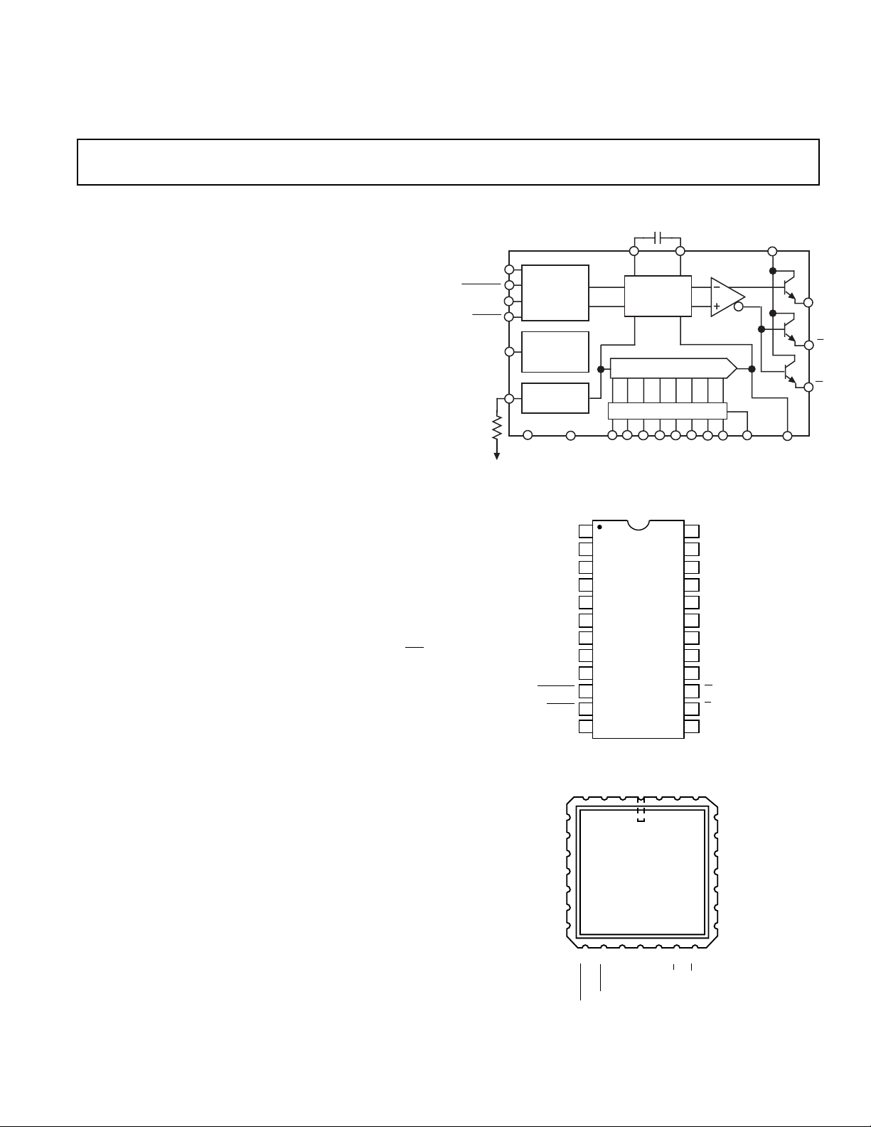
GENERAL DESCRIPTION
The AD9500 is a digitally programmable delay generator, which
provides programmed delays, selected through an 8-bit digital
code, in resolutions as small as 10 ps. The AD9500 is constructed in a high performance bipolar process, designed to
provide high speed operation for both digital and analog circuits.
The AD9500 employs differential TRIGGER and RESET
inputs which are designed primarily for ECL signal levels but
function with analog and TTL input levels. An onboard ECL
reference midpoint allows both of the inputs to be driven by
either single ended or differential ECL circuits. The AD9500
output is a complementary ECL stage, which also provides a
parallel output circuit to facilitate reset timing implementations.
The digital control data is passed to the AD9500 through a
transparent latch controlled by the LATCH ENABLE signal. In
the transparent mode, the internal DAC of the AD9500 will
attempt to follow changes at the inputs. The LATCH ENABLE
is otherwise used to strobe the digital data into the AD9500
latches.
The AD9500 is available as an industrial temperature range
device, –25°C to +85°C, and as an extended temperature range
device, –55°C to +125°C. Both grades are packaged in a 24-lead
cerdip (0.3" package width), as well as 28-leaded and leadless
surface mount packages. The AD9500 is available in versions
compliant with MIL-STD-883. Refer to the Analog Devices
Military Products Databook or current AD9500/883B data
sheet for detailed specifications.
REV. D
Information furnished by Analog Devices is believed to be accurate and
reliable. However, no responsibility is assumed by Analog Devices for its
use, nor for any infringements of patents or other rights of third parties
which may result from its use. No license is granted by implication or
otherwise under any patent or patent rights of Analog Devices.
Q
Delay Generator
AD9500
FUNCTIONAL BLOCK DIAGRAM
PIN CONFIGURATIONS
R
NC = NO CONNECT
One Technology Way, P.O. Box 9106, Norwood, MA 02062-9106, U.S.A.
Tel: 781/329-4700 World Wide Web Site: http://www.analog.com
Fax: 781/326-8703 © Analog Devices, Inc., 1999
Page 2

AD9500–SPECIFICATIONS
ABSOLUTE MAXIMUM RATINGS
1
Positive Supply Voltage (+VS) . . . . . . . . . . . . . . . . . . . . . +7 V
Negative Supply Voltage (–V
) . . . . . . . . . . . . . . . . . . . . –7 V
S
ECL COMMON to Ground Differential . . . . –2.0 V to +5.0 V
Digital Input Voltage Range . . . . . . . . . . . . . –3.5 V to +5.0 V
Trigger/Reset Input Voltage Range . . . . . . . . . . . . . . . ±5.0 V
Trigger/Reset Differential Voltage . . . . . . . . . . . . . . . . . .5.0 V
Minimum R
. . . . . . . . . . . . . . . . . . . . . . . . . . . . . . . 220 Ω
SET
Digital Output Current (
Offset Adjust Current (Sinking) . . . . . . . . . . . . . . . . . . . 4 mA
) . . . . . . . . . . . . . . . . . . . . 2 mA
Q
R
Operating Temperature Range
AD9500BP/BQ . . . . . . . . . . . . . . . . . . . . . –25°C to +85°C
AD9500TE/TQ . . . . . . . . . . . . . . . . . . . . –55°C to +125°C
Storage Temperature Range . . . . . . . . . . . . –65°C to +150°C
Junction Temperature . . . . . . . . . . . . . . . . . . . . . . . . .+175°C
Lead Soldering Temperature (10 sec) . . . . . . . . . . . . .+300°C
Digital Output Current (Q and Q) . . . . . . . . . . . . . . . 30 mA
ELECTRICAL CHARACTERISTICS
2
(Supply Voltages +VS = +5.0 V, VS = –5.2 V; C
= 0 pF; R
EXT
= 500 ⍀ unless otherwise noted)
SET
–25ⴗC to +85ⴗC –55ⴗC to +125ⴗC
Test AD9500BP/BQ AD9500TE/TQ
Parameter Level Temp Min Typ Max Min Typ Max Units
RESOLUTION 8 8 Bits
ACCURACY
3
Differential Linearity I +25°C 0.5 0.5 LSB
Integral Linearity I +25°C 1.0 1.0 LSB
Monotonicity I +25°C Guaranteed Guaranteed
DIGITAL INPUT
Logic “1” Voltage VI Full 2.0 2.0 V
Logic “0” Voltage VI Full 0.8 0.8 V
Logic “1” Current VI Full 5 5 µA
Logic “0” Current VI Full 5 5 µA
Digital Input Capacitance VI +25°C 5.5 5.5 pF
Data Setup Time
Data Hold Time
Latch Pulsewidth (t
RESET/TRIGGER INPUTS
4
5
) V +25°C 3.0 3.0 ns
LPW
6
V +25°C 0.4 0.75 0.4 0.75 ns
V +25°C 0.4 0.75 0.4 0.75 ns
TRIGGER Input Voltage Range IV Full –2.5; 4.5 –2.5; 4.5 V
RESET Input Voltage Range IV Full –2.5; 2.0 –2.5; 2.0 V
Differential Switching Voltage IV Full 40 300 40 300 mV
Input Bias Current I +25°C 4050 4050µA
VI Full 75 75 µA
Input Resistance IV +25°C4 4 kΩ
Input Capacitance IV +25°C 6.5 7.25 6.5 7.25 pF
Minimum Input Pulsewidth
t
, t
TPW
RPW
DYNAMIC PERFORMANCE
Maximum Trigger Rate IV +25°C 60 60 MHz
Minimum Propagation Delay (t
Minimum Propagation Delay TC V Full 7.5 7.5 ps/°C
Full-Scale Range TC
9
Delay Uncertainty (Jitter) V +25°C10 10 ps
Reset Propagation Delay (t
Reset-to-Trigger Holdoff (t
Trigger-to-Reset Holdoff (t
Minimum Output Pulsewidth V +25°C 3.3 3.3 ns
Output Rise Time
Output Fall Time
7
7
Delay Coefficient Settling Time (t
Linear Ramp Settling Time (t
7
8
)
PD
10
)
RD
11
)
THO
12
)
RHO
DAC
) V +25°C22 22 ns
LRS
V +25°C 2.0 2.0 ns
I +25°C 5.4 6.4 7.4 5.4 6.4 7.4 ns
V Full 0.5 0.5 ps/°C
I +25°C 5.4 6.4 7.4 5.4 6.4 7.4 ns
IV +25°C 0.2 0 0.2 0 ns
IV +25°C 2.0 1.5 2.0 1.5 ns
I +25°C 2.0 2.0 ns
I +25°C 2.0 2.0 ns
13
)
V +25°C29 29 ns
REV. D–2–
Page 3

AD9500
–25ⴗC to +85ⴗC –55ⴗC to +125ⴗC
Test AD9500BP/BQ AD9500TE/TQ
Parameter Level Temp Min Typ Max Min Typ Max Units
SUPPORT FUNCTIONS
ECL
ECL
REF
Voltage Drift
REF
14
Offset Adjust Range V Full –2 –2 mA
DIGITAL OUTPUTS
7
Logic “1” Voltage VI Full –1.1 –1.1 V
Logic “0” Voltage VI Full –1.5 –1.5 V
POWER SUPPLY
15
Positive Supply Current (+5.0 V) I +25°C 2428 2428mA
Negative Supply Current (–5.2 V) I +25°C 3742 3742mA
Nominal Power Dissipation V +25°C 312 312 mW
Power Supply Rejection Ratio
16
Full-Scale Range Sensitivity I +25°C 70 300 70 300 ps/V
Minimum Propagation Delay
Sensitivity I +25°C 150 500 150 500 ps/V
NOTES
1
Absolute maximum ratings are limiting values, to be applied individually, and beyond which serviceability of the circuit may be impaired. Functional operability under
any of these conditions is not necessarily implied. Exposure to absolute maximum rating conditions for extended periods may affect device reliability.
2
Typical thermal impedance
24-Lead Cerdip θ
28-Leadless PLCC (Plastic) θ
28-Leaded Ceramic LCC θ
3
R
= 10 kΩ (Full-scale delay = 100 ns).
SET
4
The digital data inputs must remain stable for the specified time prior to the LATCH ENABLE signal.
5
The digital data inputs must remain stable for the specified time after the LATCH ENABLE signal.
6
The TRIGGER and RESET inputs are differential and must be driven relative to one another. Both of these inputs are ECL compatible, but can also be used with
TTL logic families in a limited fashion.
7
Outputs terminated through 50 Ω resistors to –2.0 V.
8
Program Delay = 0.0 ps (Digital Data = 00H). In Operation, any programmed delays are in addition to the Minimum Propagation Delay.
9
Change in total delay through AD9500, exclusive of changes in minimum propagation delay tPD.
10
Measured from the 50% transition point of the reset signal input, to the 50% transition point of the resetting output.
11
Minimum time from falling edge of RESET to triggering input, to ensure a valid output event.
12
Minimum time from triggering event to rising edge of RESET, to ensure a valid output event.
13
Measured from the LATCH ENABLE input to the point when the AD9500 becomes 8-bit accurate again, after a full-scale change in the programmed delay.
14
Standard 10K and 10KH ECL families operate with a 1.1 mV/°C drift by design.
15
Supply voltages should remain stable within ±5% for normal operation.
16
Measured at ±5% of –V
Specifications subject to change without notice.
and +VS.
S
= 56°C/W; θJC = 16°C/W
JA
= 60°C/W; θJC = 22°C/W
JA
= 69°C/W; θJC = 25°C/W
JA
IV +25°C –1.4 –1.3 –1.2 –1.4 –1.3 –1.2 V
V Full 1.1 1.1 mV/°C
VI Full 30 30 mA
VI Full 44 44 mA
EXPLANATION OF TEST LEVELS
Test Level
I – 100% production tested.
II – 100% production tested at +25°C, and sample tested at
specified temperatures.
III – Periodically sample tested.
IV – Parameter is guaranteed by design and characterization
testing.
V – Parameter is a typical value only.
VI – All devices are 100% production tested at +25°C. 100%
production tested at temperature extremes for extended
temperature devices; sample tested at temperature extremes for commercial/industrial devices.
REV. D
ORDERING GUIDE
Temperature Package Package
Model Ranges Descriptions Options
AD9500BP –25°C to +85°C 28-Leadless PLCC (Plastic),
Industrial Temperature P-28A
AD9500BQ –25°C to +85°C 24-Lead Cerdip,
Industrial Temperature Q-24
AD9500TE –55°C to +125°C 28-Leaded LCC,
Extended Temperature E-28A
AD9500TQ –55°C to +125°C 24-Lead Cerdip,
Extended Temperature Q-24
–3–
Page 4

AD9500
PIN FUNCTION DESCRIPTIONS
Pin Name Description
D
4–D6
D
(MSB) One of eight digital inputs used to set the programmed delay. D7 (MSB) is the most significant bit of the
7
ECL
REF
OFFSET ADJUST The OFFSET ADJUST is used to adjust the minimum propagation delay (t
C
S
+V
S
TRIGGER Noninverted input of the edge-sensitive differential trigger input stage. The output at Q will be delayed by
TRIGGER Inverted input of the edge-sensitive differential trigger input stage. The output at Q will be delayed by the
RESET Inverted input of the level-sensitive differential reset input stage. The output at Q will be reset after a signal
RESET Noninverted input of the level-sensitive differential reset input stage. The output at Q will be reset after a
Q One of two complementary ECL outputs. A “triggering” event at the inputs will produce a logic HIGH on
Q One of two complementary ECL outputs. A “triggering” event at the inputs will produce a logic LOW on
Q
R
ECL COMMON The collector common for the ECL output stage. The collector common may be tied to +5.0 V, but nor-
–V
S
R
S
GROUND The ground return for the TTL and analog inputs.
LATCH ENABLE Transparent TTL latch control line. A logic HIGH on the LATCH ENABLE freezes the digital code at the
D
(LSB) One of eight digital inputs used to set the programmed delay. D0 (LSB) is the least significant bit of the
0
D3–D
1
One of eight digital inputs used to set the programmed delay.
digital input word.
ECL midpoint reference, nominally –1.3 V. Use of the ECL
allows either of the TRIGGER or RESET
REF
inputs to be configured for single-ended ECL inputs.
), by pulling or pushing a
PD
small current out of or into the pin.
CS allows the full-scale range to be extended by using an external timing capacitor. The value of C
connected between C
See R
S
(C
INTERNAL
= 10 pF).
and +V
S
, may range from no external capacitance to 0.1 µF+.
S
EXT
,
Positive supply terminal, nominally +5.0 V.
the programmed delay, after the triggering event. The programmed delay is set by the digital input word.
The TRIGGER input must be driven in conjunction with the TRIGGER input.
programmed delay, after the triggering event. The programmed delay is set by the digital input word. The
TRIGGER input must be driven in conjunction with the TRIGGER input.
is received at the reset inputs. In the “minimum configuration,” the minimum output pulsewidth will be
equal to the “reset propagation delay,” t
. The RESET input must be driven in conjunction with the
RD
RESET input.
signal is received at the reset inputs. In the “minimum configuration,” the minimum output pulsewidth will
be equal to the “reset propagation delay,” t
. The RESET input must be driven in conjunction with the
RD
RESET input.
the Q output. A “resetting” event at the inputs will produce a logic LOW on the Q output.
the Q output. A “resetting” event at the inputs will produce a logic HIGH on the Q output.
output is parallel to the Q output. The
Q
R
ing output pulsewidths. A “triggering” event at the inputs will produce a logic LOW on the
“resetting” event at the inputs will produce a logic HIGH on the
output is typically used to drive delaying circuits for extend-
Q
R
output.
Q
R
output. A
Q
R
mally it is tied to the circuit ground for standard ECL outputs.
Negative supply terminal, nominally –5.2 V.
RS is the reference current setting terminal. An external setting resistor, R
determines the internal reference current. See C
–V
S
(250 Ω ≤ R
S
≤ 50 kΩ).
SET
, connected between RS and
SET
logic inputs. A logic LOW on the LATCH ENABLE allows the internal current levels to be continuously
updated through the logic inputs D
thru D7.
0
digital input word.
One of eight digital inputs used to set the programmed delay.
–4–
REV. D
Page 5

AD9500
DIE LAYOUT
Figure 1. System Timing Diagram
MECHANICAL INFORMATION
Die Dimensions . . . . . . . . . . . . . . . 104 ⫻ 103 ⫻ 18 (max) mils
Pad Dimensions . . . . . . . . . . . . . . . . . . . . . . . 4 ⫻ 4 (min) mils
Metalization . . . . . . . . . . . . . . . . . . . . . . . . . . . . . . . Aluminum
Backing . . . . . . . . . . . . . . . . . . . . . . . . . . . . . . . . . . . . . . None
Substrate Potential . . . . . . . . . . . . . . . . . . . . . . . . . . . . . . .–V
Passivation . . . . . . . . . . . . . . . . . . . . . . . . . . . . . . . . Oxynitride
Die Attach . . . . . . . . . . . . . . . . . . . . . . . . . . . . . .Gold Eutectic
Bond Wire . . . . . . . . 1.25 mil, Aluminum; Ultrasonic Bonding
S
or 1 mil, Gold; Gold Ball Bonding
REV. D
–5–
Page 6

AD9500
Figure 2. Input/Output Circuits
–6–
REV. D
Page 7

INSIDE THE AD9500
The heart of the AD9500 is the linear ramp generator. A triggering event at the input of the AD9500 initiates the ramp cycle.
As the ramp voltage falls, it will eventually go below the threshold set up by the internal DAC (digital-to-analog converter). A
comparator monitors both the linear ramp voltage and the DAC
threshold level. The output of the comparator serves as the
output for the AD9500, and the interval from the trigger until
the output switches is the total delay time of the AD9500.
The total delay through the AD9500 is made up of two components. The first is the full-scale programmed delay, t
determined by R
SET
and C
. The second component of the
EXT
D (max)
,
total delay is the minimum propagation delay through the
AD9500 (t
). The full-scale delay is variable from 2.5 ns to
PD
greater than 1 ms. The internal DAC is capable of generating
256 separate programmed delays within the full-scale range (this
gives 10 ps increments for a 2.5 ns full-scale setting).
The actual programmed delay is directly related to both the
digital control data (digital data to the internal DAC) and the
RC time constant established by R
SET
and C
. The specific
EXT
relationship is as follows:
Total Delay = Minimum Propagation Delay +
Programmed Delay
= t
+ (digital value/256) R
PD
SET
(C
+ 10 pF)
EXT
Figure 3. Typical Programmed Delay Ranges
The internal DAC determines the programmed delay by way of
the threshold level at its output. The LATCH ENABLE control
for the onboard latch is active (latches) logic “HIGH.” In the
logic “LOW” state, the latch is transparent, and the internal
DAC will attempt to follow changes at the digital data inputs.
Both the LATCH ENABLE control and the data inputs are
TTL compatible. The internal DAC may be updated at any
time, but full timing accuracy may not be attained unless triggering events are held off until after the DAC settling time
).
(t
DAC
AD9500
Figure 4. Internal Timing Diagram
On resetting, the ramp voltage held in the timing capacitor
+ 10 pF) is discharged. The AD9500 discharges the bulk
(C
EXT
of the ramp voltage very quickly, but to maintain absolute accuracy, subsequent triggering events should be held off until after
the linear ramp settling time (t
high frequency triggering at a constant rate will not be affected
by the slight settling errors since they will be constant for fixed
reset-to-trigger cycles.
The RESET and TRIGGER inputs of the AD9500 are differential and must be driven relative to one another. Accordingly, the
TRIGGER and RESET inputs are ideally suited for analog or
complementary input signals. Single-ended ECL input signals
can be accommodated by using the ECL midpoint reference
(ECL
) to drive one side of the differential inputs.
REF
The output of the AD9500 consists of both Q and Q driver
stages, as well as the
extending the output pulsewidth. In the most direct reset con-
output which is used primarily for
Q
R
figuration, either the Q or the Q output is tied to the respective
RESET input. This generates a delayed output pulse with a
duration equal to the reset delay time (t
6 ns. Note that the reset delay time (t
very small programmed delay settings. The duration of the
output pulse can be extended by driving the reset inputs with the
output through an RC network (see “Extended Output
Q
R
Pulsewidth” application). Using the
reset circuit avoids loading the Q or Q outputs.
Values in the specification table are based on 5 ns FSR test
conditions. Nearly all dynamic specifications degrade for longer
full scales. For details of performance change, request the application note “Using Digitally Programmable Delay Generators.”
). Applications which employ
LRS
) of approximately
RD
) becomes extended for
RD
output to drive the
Q
R
REV. D
–7–
Page 8

AD9500
APPLICATIONS
The AD9500 is a very versatile device that is not difficult to use.
Essentially there are only a few basic configurations which can
be extended into a number of applications. The TRIGGER and
RESET inputs of the AD9500 can be treated as single ended, or
as differential, which allows the AD9500 to operate with a wide
range of signal sources. The output pulse from the AD9500 can
be reset in one of two ways, either immediately by driving the
RESET inputs with the output itself, or in a delayed mode.
MINIMUM CONFIGURATION
The minimum configuration uses only one of the TRIGGER
inputs. The other is connected to the ECL reference midpoint,
ECL
. This allows the AD9500 to be triggered with standard
REF
10K or 10KH ECL signals. Once a triggering event occurs, the
Q output will go into the logic HIGH state, and the Q output
will go into the logic LOW state after the programmed delay.
The Q output is then used to drive the RESET input, causing
the AD9500 to reset itself. The result is a delayed output pulse
which is only as wide as the reset propagation delay (t
RD
).
the Q and the Q outputs are completely free for other uses. Q
has limited current drive; the minimum resistance for R
should
D
be 4 kΩ.
Figure 6. Extended Output Pulsewidth Configuration
MULTICHANNEL DESKEWING
Perhaps the most appropriate use of the AD9500 is in multiple
delay matching applications. Slight differences in impedance
and cable length can create large timing skews within a highspeed system. Much of this skew can be eliminated by running
each signal through an AD9500. With one line used as a standard, the programmed delays of the other AD9500s are adjusted
to eliminate the timing skews. With the very fine timing adjustments possible from the AD9500 (as small as 10 ps), nearly any
high-speed system should be able to automatically adjust itself
to extremely tight tolerances.
Figure 5. Single Input–Minimum Timing Configuration
EXTENDED OUTPUT PULSEWIDTHS
The extended pulse configuration is similar to the minimum
configuration. The difference here is that the output pulsewidth
has been extended. Operation is identical in terms of triggering
the AD9500; the functional difference is in the resetting circuit.
In this case the
through a resistor/capacitor charging network. The charging
output is used to drive the RESET input
Q
R
network will cause the signal at the RESET input to fall more
slowly, which will extend the output pulsewidth. An added
benefit of the extended pulsewidth configurations is that both
–8–
Figure 7. Multiple Delay Matching
REV. D
Page 9

AD9500
MEASURING UNKNOWN DELAYS
Two AD9500s can be combined to measure delays with a high
degree of precision. One AD9500 is set with little or no programmed delay, and its output is used to drive the unknown
delay circuit, which in turn drives the input of a “D” type flipflop. The second AD9500 is triggered along with the first, and
its output provides a clocking signal for the flip-flop. The programmed delay of the second AD9500 is then varied to detect
the output edge from the unknown delay circuit.
Detecting the output edge is relatively straightforward. If the
programmed delay through the second AD9500 is too long, the
flip-flop output will be at logic HIGH. If, on the other hand, the
programmed delay through the second AD9500 is too short, the
flip-flop output will be at logic LOW. When the programmed
delay is properly adjusted, the flip-flop will likely bounce between logic HIGH and logic LOW. The digital code value used
to create the second programmed delay is a direct indication of
the delay through the unknown circuit. The most accurate results can only be attained by calibrating the system without the
unknown delay circuit in place.
Figure 8. Measuring Unknown Delays
equals the DAC threshold. By varying the DAC threshold level
and adjusting the second AD9500 programmed delay, a point
by point reconstruction of the ac waveform can be created.
Figure 9. Measuring AC Waveforms
PROGRAMMABLE OSCILLATOR
Another interesting use of the AD9500 is in a digitally programmable oscillator. The highly accurate delays generated by the
AD9500 can be exploited to create a ring oscillator with variable
duty cycle. The delayed output of the first AD9500 is used to
drive the TRIGGER input of the second AD9500. The output
of the second AD9500, in turn, is used to drive the TRIGGER
input of the first AD9500. Together the two devices will alternately trigger each other creating two pulse chains on the outputs.
The total delay through both AD9500s combined, determines
the period of the oscillation frequency. The duty cycle can be
controlled by using the outputs to drive the SET and RESET
inputs of a flip-flop. The total delay through the first AD9500
will control the flip-flop logic LOW output pulsewidth, and the
second AD9500 will control the flip-flop logic HIGH output
pulsewidth.
MEASURING HIGH SPEED AC WAVEFORMS
The same circuitry used to measure unknown delays can be
extended to measure the time response of high speed ac waveforms. With the addition of a digital-to-analog converter and an
analog comparator, the circuit functions very much like the
previous application. The DAC sets a threshold level which
drives one of the differential comparator inputs. The other comparator input is driven by the device under test (DUT). The
output of the first AD9500 causes the DUT to produce an
output. The second AD9500, which is also triggered along with
the first AD9500, strobes the comparator latch enable.
If the DUT output is greater than the DAC threshold when the
comparator is latched, the comparator output will be at logic
HIGH. If the output is below the DAC threshold, the comparator will be at logic LOW. The programmed delay setting of the
second AD9500 is adjusted to the point where the DUT output
Figure 10. Ring Oscillator
REV. D
–9–
Page 10

AD9500
LAYOUT CONSIDERATIONS
The AD9500 is a precision timing device, and as such high
frequency design techniques must be employed to achieve the
best performance. The use of a low impedance ground plane is
particularly important. Ideally the ground plane should be on
the component side of the layout and extend under the
AD9500, to shield it from system timing signals. Sockets pose a
special problem for a circuit like the AD9500 because of the
additional inter-lead capacitance they create. If sockets must be
used, pin sockets are generally preferred. Power supply decou-
pling is also critical to a high-speed design; a 0.1 µF ceramic
capacitor and a 0.01 µF mica capacitor for both power supplies
should be very effective. DAC threshold stability can be improved
by decoupling the OFFSET ADJUST pin to +5.0 V (note that this
will lengthen the DAC settling time, t
DELAY OFFSET ADJUSTMENTS
DAC
)
As the full-scale delay is increased, a component of the minimum propagation delay also increases. This is caused by the
additional time required by the ramp (now with a much “flatter”
slope) to fall below the DAC threshold corresponding to the
minimum propagation delay (t
). One means of decreasing the
PD
minimum propagation delay (when the full-scale delay, set by
R
SET
and C
is large) is to offset the internal DAC threshold
EXT
toward the initial ramp levels, thus reducing the time for the
internal ramp to cross the threshold once the AD9500 is triggered.
GENERAL PERFORMANCE ENHANCEMENTS
High speed operation is generally more consistent if C
EXT
is
kept small (i.e., no external capacitor) to maintain small discharge time constants. Integral linearity, however, benefits from
larger values of C
by buffering small system spikes and
EXT
surges. Another means of improving integral linearity is to draw
a small current (≈200 µA) out of the OFFSET ADJUST pin
with a 47 kΩ pull-down resistor. This has the effect of moving
the internal DAC reference levels into a relatively more linear
region of the ramp. This technique is generally only useful for
small full-scale delay configurations. Its use with larger full-scale
delays will extend the minimum propagation delay (t
). A pull-
PD
up resistor to +5.0 V creates the opposite effect by reducing the
minimum propagation delay (t
reset propagation delay (t
) at the expense of increased
PD
) and degraded linearity (see OFF-
RD
SET matching circuit).
Caution should be used when applying high slew rate data at the
inputs of the AD9500. For data inputs with slew rates in excess
of 1 V/ns, a 100 Ω series resistor should be utilized in the data
path.
An external DAC can be used with the AD9500 for increased
resolution and higher update rates. For the most part, a standard ECL DAC, operating between +5.0 V and ground, should
work with the AD9500. The output of the external DAC must
be connected to the OFFSET ADJUST pin of the AD9500 with
the internal DAC turned off (D
thru D7 at logic LOW). For
0
normal operation, the external DAC output should range from
0 mA to –2 mA (sinking).
Figure 11. The Offset Adjust Pin Can Be Used to Match
Several AD9500s
The DAC levels are offset toward the initial ramp level by injecting a small current into the offset adjust pin. Note, however,
that the ramp start-up region is less linear than the later portions
of the ramp, which is the primary reason for the built-in offset.
If the minimum propagation delay is kept above 5 ns (the linear
portion of the ramp), no significant degradation in linearity
should result. This concept can be extended to match the actual
propagation delays of several AD9500s, by injecting or sinking
a small current (<2 mA) into or out of each of the OFFSET
ADJUST pins.
–10–
Figure 12. Operation with External DAC
REV. D
Page 11

OUTLINE DIMENSIONS
1
28
5
11
12
18
26
BOTTOM
VIEW
19
4
25
0.028 (0.71)
0.022 (0.56)
45° TYP
0.015 (0.38)
MIN
0.055 (1.40)
0.045 (1.14)
0.050
(1.27)
BSC
0.075
(1.91)
REF
0.011 (0.28)
0.007 (0.18)
R TYP
0.095 (2.41)
0.075 (1.90)
0.150
(3.51)
BSC
0.300 (7.62)
BSC
0.200
(5.08)
BSC
0.075
(1.91)
REF
0.458 (11.63)
0.442 (11.23)
SQ
0.458
(11.63)
MAX
SQ
0.100 (2.54)
0.064 (1.63)
0.088 (2.24)
0.054 (1.37)
Dimensions shown in inches and (mm).
24-Lead Cerdip
(Q-24)
0.005 (0.13) MIN 0.098 (2.49) MAX
AD9500
0.200 (5.08)
MAX
0.200 (5.08)
0.125 (3.18)
24
1
PIN 1
0.023 (0.58)
0.014 (0.36)
1.280 (32.51) MAX
0.100 (2.54)
BSC
28-Leaded LCC
(E-28A)
13
12
0.070 (1.78)
0.030 (0.76)
0.310 (7.87)
0.220 (5.59)
0.060 (1.52)
0.015 (0.38)
0.150
(3.81)
MIN
SEATING
PLANE
0.320 (8.13)
0.290 (7.37)
15°
0°
C1137d–0–4/99
0.015 (0.38)
0.008 (0.20)
REV. D
0.048 (1.21)
0.042 (1.07)
0.048 (1.21)
0.042 (1.07)
0.020
(0.50)
R
4
5
IDENTIFIER
TOP VIEW
(PINS DOWN)
11
12
0.456 (11.58)
0.450 (11.43)
0.495 (12.57)
0.485 (12.32)
28-Leadless PLCC
(P-28A)
0.056 (1.42)
0.042 (1.07)
26
25
PIN 1
0.050
(1.27)
BSC
19
18
SQ
SQ
–11–
0.180 (4.57)
0.165 (4.19)
0.110 (2.79)
0.085 (2.16)
0.025 (0.63)
0.015 (0.38)
0.021 (0.53)
0.013 (0.33)
0.032 (0.81)
0.026 (0.66)
0.040 (1.01)
0.025 (0.64)
0.430 (10.92)
0.390 (9.91)
PRINTED IN U.S.A.
 Loading...