

Page 1
12-Bit, 105 MSPS/125 MSPS,
FEATURES
IF sampling up to 350 MHz
SNR: 67.5 dB, f
SFDR: 83 dBc, f
SFDR: 72 dBc, f
2 V p-p analog input range
On-chip clock duty cycle stabilization
On-chip reference and track-and-hold
SFDR optimization circuit
Excellent linearity
DNL: ±0.25 LSB (typical)
INL: ±0.5 LSB (typical)
750 MHz full power analog bandwidth
Power dissipation: 1.35 W (typical) at 125 MSPS
Twos complement or offset binary data format
5.0 V analog supply operation
2.5 V to 3.3 V T TL/CMOS outputs
APPLICATIONS
Cellular infrastructure communication systems
3G single- and multicarrier receivers
IF sampling schemes
Wideband carrier frequency systems
Point-to-point radios
LMDS, wireless broadband
MMDS base station units
Cable reverse path
Communications test equipment
Radar and satellite ground systems
GENERAL INTRODUCTION
The AD9433 is a 12-bit, monolithic sampling analog-to-digital
converter (ADC) with an on-chip track-and-hold circuit and is
designed for ease of use. The product operates up to a 125 MSPS
conversion rate and is optimized for outstanding dynamic performance in wideband and high IF carrier systems.
The ADC requires a 5 V analog power supply and a differential
encode clock for full performance operation. No external reference or driver components are required for many applications.
The digital outputs are TTL-/CMOS-compatible, and a separate
output power supply pin supports interfacing with 3.3 V or
2.5 V logic.
up to Nyquist at 105 MSPS
IN
= 70 MHz at 105 MSPS
IN
= 150 MHz at 105 MSPS
IN
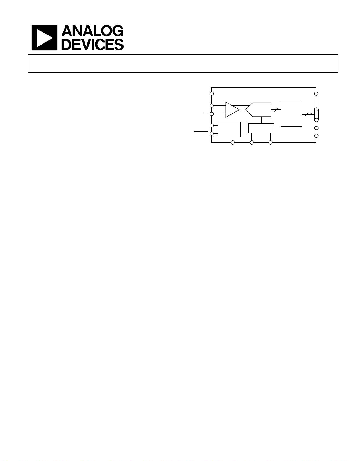
IF Sampling ADC
AD9433
FUNCTIONAL BLOCK DIAGRAM
V
AIN
AIN
ENCODE
ENCODE
CC
T/H
ENCODE
TIMING
GND VREFOUT VREFIN
PIPELINE
ADC
REF
Figure 1.
12
AD9433
OUTPUT
STAGING
A user-selectable, on-chip proprietary circuit optimizes
spurious-free dynamic range (SFDR) vs. signal-to-noise and
distortion (SINAD) ratio performance for different input signal
frequencies, providing as much as 83 dBc SFDR performance
over the dc to 70 MHz band.
The encode clock supports either differential or single-ended
input and is PECL-compatible. The output format is userselectable for offset binary or twos complement and provides
an overrange (OR) signal.
Fabricated on an advanced BiCMOS process, the AD9433 is
available in a 52-lead thin quad flat package (TQFP_EP) that
is specified over the industrial temperature range of −40°C to
+85°C. The AD9433 is pin-compatible with the AD9432.
PRODUCT HIGHLIGHTS
1. IF Sampling.
The AD9433 maintains outstanding ac performance up to
input frequencies of 350 MHz. Suitable for 3G wideband
cellular IF sampling receivers.
2. Pin-Compatibility with the AD9432.
The AD9433 has the same footprint and pin layout as the
AD9432 12-bit 80 MSPS/105 MSPS ADC.
3. SFDR Performance.
A user-selectable, on-chip circuit optimizes SFDR
performance as much as 83 dBc from dc to 70 MHz.
4. Sampling Rate.
At 125 MSPS, the AD9433 is ideally suited for wireless and
wired broadband applications such as LMDS/MMDS and
cable reverse path.
V
DD
12
D11 TO D0
DFS
SFDR
MODE
01977-001
Rev. A
Information furnished by Analog Devices is believed to be accurate and reliable. However, no
responsibility is assumed by Analog Devices for its use, nor for any infringements of patents or other
rights of third parties that may result from its use. Specifications subject to change without notice. No
license is granted by implication or otherwise under any patent or patent rights of Analog Devices.
Trademarks and registered trademarks are the property of their respective owners.
One Technology Way, P.O. Box 9106, Norwood, MA 02062-9106, U.S.A.
Tel: 781.329.4700 www.analog.com
Fax: 781.461.3113 ©2001–2009 Analog Devices, Inc. All rights reserved.
Page 2

AD9433
TABLE OF CONTENTS
Features .............................................................................................. 1
Applications ....................................................................................... 1
General Introduction ....................................................................... 1
Functional Block Diagram .............................................................. 1
Product Highlights ........................................................................... 1
Revision History ............................................................................... 2
Specifications ..................................................................................... 3
DC Specifications ......................................................................... 3
AC Specifications .......................................................................... 4
Switching Specifications .............................................................. 5
Timing Diagram ........................................................................... 5
Absolute Maximum Ratings ............................................................ 6
Explanation of Test Levels ........................................................... 6
Thermal Characteristics .............................................................. 6
ESD Caution .................................................................................. 6
Pin Configuration and Function Descriptions ............................. 7
Typical Performance Characteristics ..............................................8
Terminology .................................................................................... 14
Equivalent Circuits ......................................................................... 16
Theory of Operation ...................................................................... 17
Encode Input ............................................................................... 17
Encode Voltage Level Definition .............................................. 17
Analog Input ............................................................................... 18
SFDR Optimization.................................................................... 18
Digital Outputs ........................................................................... 18
Voltage Reference ....................................................................... 18
Timing ......................................................................................... 18
Applications Information .............................................................. 19
Layout Information .................................................................... 19
Replacing the AD9432 with the AD9433 ................................ 19
Outline Dimensions ....................................................................... 20
Ordering Guide .......................................................................... 20
REVISION HISTORY
6/09—Rev. 0 to Rev. A
Updated Format .................................................................. Universal
Reorganized Layout ............................................................ Universal
Added TQFP_EP Package ................................................. Universal
Deleted LQFP_ED Package ............................................... Universal
Changes to Thermal Characteristics Section ................................ 6
Changes to Pin Configuration and Function Descriptions
Section ................................................................................................ 7
Deleted Evaluation Board Section ................................................ 16
Updated Outline Dimensions ....................................................... 20
Changes to Ordering Guide .......................................................... 20
10/01—Revision 0: Initial Version
Rev. A | Page 2 of 20
Page 3

AD9433
SPECIFICATIONS
DC SPECIFICATIONS
VDD = 3.3 V, VCC = 5 V; internal reference; differential encode input, unless otherwise noted.
Table 1.
Test 105 MSPS 125 MSPS
Parameter Temp Level Min Typ Max Min Typ Max Unit
RESOLUTION 12 12 Bits
ACCURACY
No Missing Codes Full VI Guaranteed Guaranteed
Offset Error Full VI −5 0 +5 −5 0 +5 mV
Gain Error
Differential Nonlinearity (DNL)225°C I −0.75 ±0.25 +0.75 −0.75 ±0.3 +0.75 LSB
Full VI −1 +1 −1 +1 LSB
Integral Nonlinearity (INL)
Full VI −1.3 +1.3 −1.3 +1.3 LSB
THERMAL DRIFT
Offset Error Full V −50 −50 ppm/°C
Gain Error
Reference Full V ±80 ±80 ppm/°C
REFERENCE
Internal Reference Voltage
Output Current (VREFOUT) Full V 100 100 μA
Input Current (VREFIN) Full IV 50 50 μA
ANALOG INPUTS (AIN, AIN)
Input Voltage Range Full V 2.0 2.0 V p-p
Common-Mode Voltage Full V 4.0 4.0 V
Input Resistance Full VI 2 3 4 2 3 4 kΩ
Input Capacitance Full V 4 4 pF
Analog Bandwidth, Full Power Full V 750 750 MHz
POWER SUPPLY
VCC Full IV 4.75 5.0 5.25 4.75 5.0 5.25 V
VDD Full IV 2.7 3.3 2.7 3.3 V
Power Dissipation
I
VCC
I
VDD
Power Supply Rejection Ratio
ENCODE INPUTS
Internal Common-Mode Bias Full V 3.75 3.75 V
Differential Input
Input Voltage Range Full IV −0.5 VCC + 0.05 −0.5 VCC + 0.05 V
Input Common-Mode Range Full IV 2.0 4.25 2.0 4.25 V
Input Resistance Full VI 6 6 kΩ
Input Capacitance 25°C V 3 3 pF
DIGITAL INPUTS
Input High Voltage Full I 2.0 2.0 V
Input Low Voltage Full I 0.8 0.8 V
Input High Current (VIN = 5 V) Full V 50 50 μA
Input Low Current (VIN = 0 V) Full V 50 50 μA
1
2
1
Full V −125 −125 ppm/°C
25°C I −7 ±1 +3 −7 ±1 +3 % FS
25°C I −1.0 ±0.5 +1.0 −1.0 ±0.5 +1.0 LSB
Full I 2.4 2.5 2.6 2.4 2.5 2.6 V
(VREFOUT)
3
3
3
Full VI 12.5 14 16 18 mA
Full VI 1275 1425 1350 1500 mW
Full VI 255 285 270 300 mA
25°C I ±3 ±3 mV/V
(PSRR)
Full V 500 500 mV
(ENCODE, ENCODE
)
Rev. A | Page 3 of 20
Page 4

AD9433
Test 105 MSPS 125 MSPS
Parameter Temp Level Min Typ Max Min Typ Max Unit
DIGITAL OUTPUTS
Logic 1 Voltage Full VI VDD − 0.05 VDD − 0.05 V
Logic 0 Voltage Full VI 0.05 0.05 V
Output Coding Twos complement or offset binary Twos complement or offset binary
1
Gain error and gain temperature coefficients are based on the ADC only (with a fixed 2.5 V external reference and a 2 V p-p differential analog input).
2
SFDR mode disabled (SFDR MODE = GND) for DNL and INL specifications.
3
Power dissipation measured with rated encode and a dc analog input (outputs static, I
AC SPECIFICATIONS
VDD = 3.3 V, VCC = 5 V; differential encode input, unless otherwise noted.
Table 2.
Test 105 MSPS 125 MSPS
Parameter Temp Level Min Typ Max Min Typ Max Unit
DYNAMIC PERFORMANCE
Signal-to-Noise Ratio (SNR) (Without Harmonics)
fIN = 10.3 MHz 25°C I 66.5 68.0 66.0 67.7 dB
fIN = 49 MHz 25°C I 65.5 67.5 64.0 66.0 dB
fIN = 70 MHz 25°C V 67.0 65.4 dB
fIN = 150 MHz 25°C V 65.4 62.0 dB
fIN = 250 MHz 25°C V 63.7 60.0 dB
Signal-to-Noise and Distortion (SINAD) Ratio
(with Harmonics)
fIN = 10.3 MHz 25°C I 66.0 68.0 65.0 67.0 dB
fIN = 49 MHz 25°C I 64.0 67.5 63.5 65.5 dB
fIN = 70 MHz 25°C V 66.9 64.5 dB
fIN = 150 MHz 25°C V 64.0 61.5 dB
fIN = 250 MHz 25°C V 61.2 57.7 dB
Effective Number of Bits (ENOB)
fIN = 10.3 MHz 25°C I 11.1 10.9 Bits
fIN = 49 MHz 25°C I 11.0 10.7 Bits
fIN = 70 MHz 25°C V 10.9 10.6 Bits
fIN = 150 MHz 25°C V 10.4 10.0 Bits
fIN = 250 MHz 25°C V 9.9 9.4 Bits
Second-Order and Third-Order Harmonic
Distortion
fIN = 10.3 MHz 25°C I −78 −85 −76 −85 dBc
fIN = 49 MHz 25°C I −73 −80 −72 −76 dBc
fIN = 70 MHz 25°C V −83 −78 dBc
fIN = 150 MHz 25°C V −72 −67 dBc
fIN = 250 MHz 25°C V −67 −65 dBc
Worst Other Harmonic or Spur (Excluding
Second-Order and Third-Order Harmonics)
fIN = 10.3 MHz 25°C I −88 −92 −84 −90 dBc
fIN = 49 MHz 25°C I −82 −89 −82 −87 dBc
fIN = 70 MHz 25°C V −87 −85 dBc
fIN = 150 MHz 25°C V −87 −84 dBc
fIN = 250 MHz 25°C V −85 −76 dBc
Two-Tone Intermodulation Distortion (IMD3)
f
= 49.3 MHz; f
IN1
f
= 150 MHz; f
IN1
1
SNR/harmonics based on an analog input voltage of −0.5 dBFS referenced to a 2 V full-scale input range. Harmonics are specified with the SFDR mode enabled
(SFDR MODE = 5 V). SNR/SINAD specified with the SFDR mode disabled (SFDR MODE = ground).
1
= 50.3 MHz 25°C V −92 −90 dBc
IN2
= 151 MHz 25°C V −80 −76 dBc
IN2
VDD
= 0). I
VCC
and I
measured with 10.3 MHz analog input @ −0.5 dBFS.
VDD
Rev. A | Page 4 of 20
Page 5
AD9433
SWITCHING SPECIFICATIONS
VDD = 3.3 V, VCC = 5 V; differential encode input, unless otherwise noted.
Table 3.
Test 105 MSPS 125 MSPS
Parameter Temp Level Min Typ Max Min Typ Max Unit
Encode Rate Full IV 10 105 10 125 MSPS
Encode Pulse Width High (tEH) Full IV 2.9 2.4 ns
Encode Pulse Width Low (tEL) Full IV 2.9 2.4 ns
Aperture Delay (tA) 25°C V 2.1 2.1 ns
Aperture Uncertainty (Jitter)
Output Valid Time (tV)
Output Propagation Delay (tPD)
Output Rise Time (tR)
Output Fall Time (tF)
2
Out-of-Range Recovery Time 25°C V 2 2 ns
Transient Response Time 25°C V 2 2 ns
Latency Full IV 10 10 Cycles
1
Aperture uncertainty includes contribution of the AD9433, crystal clock reference, and encode drive circuit.
2
tV and tPD are measured from the transition points of the ENCODE input to the 50%/50% levels of the digital output swing. The digital output load during testing is not
to exceed an ac load of 10 pF or a dc current of 50 μA. Rise and fall times are measured from 10% to 90%.
1
2
2
2
Full VI 4.0 5.5 4.0 5.5 ns
25°C V 0.25 0.25 ps rms
Full VI 2.5 4.0 2.5 4.0 ns
Full V 2.1 2.1 ns
Full V 1.9 1.9 ns
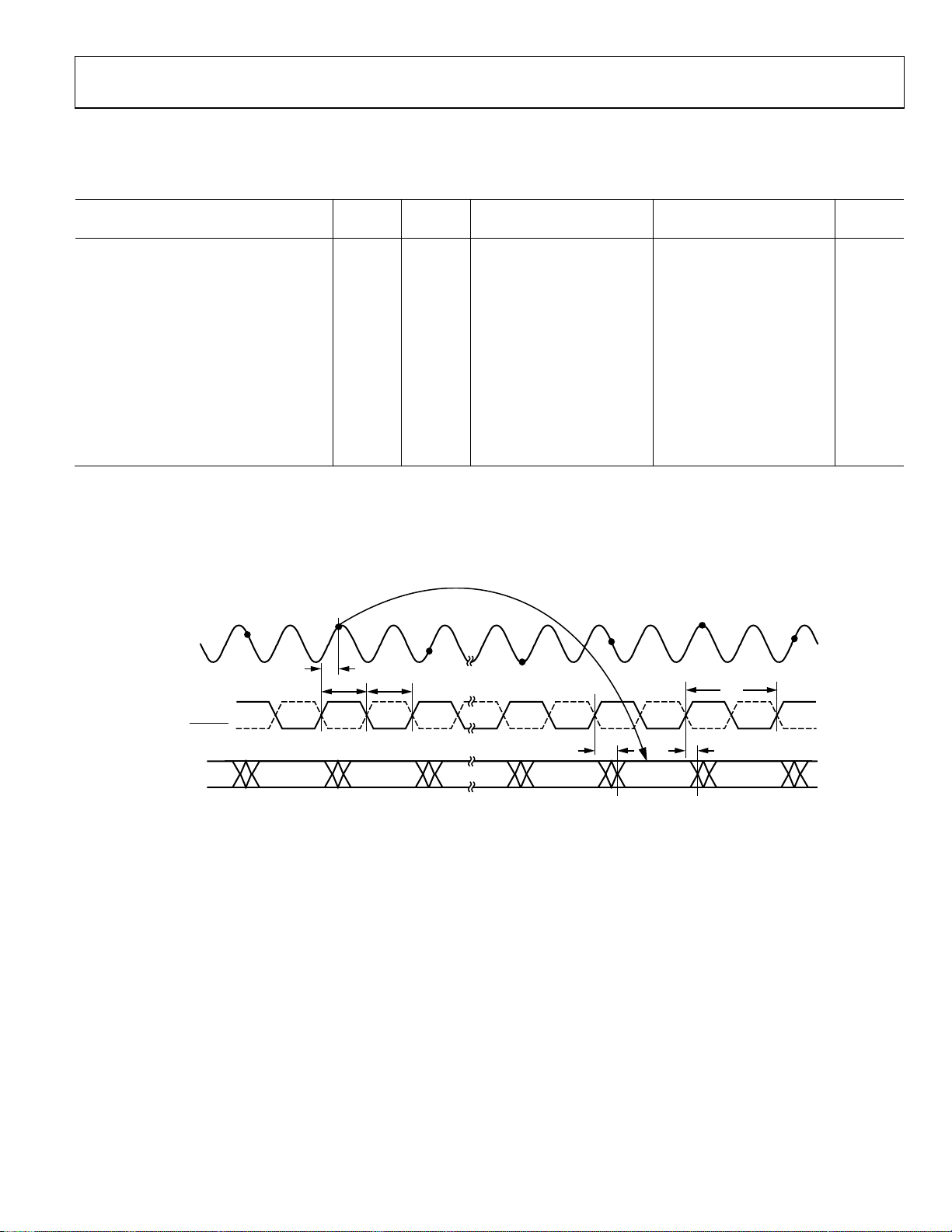
TIMING DIAGRAM
AIN
ENCODE
ENCODE
D11 TO D0
SAMPLE N – 1
DATA N – 11 DATA N – 10 DATA N – 1 DATA N DATA N + 1
SAMPLE N
t
A
SAMPLE N + 9
t
EL
EH
DATA
N – 9
SAMPLE N + 1
t
SAMPLE N + 8
DATA
N – 2
t
PD
SAMPLE N + 10
1/
t
V
f
S
01977-003
Figure 2. Timing Diagram
Rev. A | Page 5 of 20
Page 6
AD9433
ABSOLUTE MAXIMUM RATINGS
Table 4.
Parameter Rating
VDD −0.5 V to +6.0 V
VCC −0.5 V to +6.0 V
Analog Inputs −0.5 V to VCC + 0.5 V
Digital Inputs −0.5 V to VDD + 0.5 V
Digital Output Current 20 mA
Operating Temperature Range (TA) −40°C to +85°C
Storage Temperature Range −65°C to +125°C
Maximum Junction Temperature (TJ) 150°C
Stresses above those listed under Absolute Maximum Ratings
may cause permanent damage to the device. This is a stress
rating only; functional operation of the device at these or any
other conditions above those indicated in the operational
section of this specification is not implied. Exposure to absolute
maximum rating conditions for extended periods may affect
device reliability.
EXPLANATION OF TEST LEVELS
I 100% production tested.
II 100% production tested at 25°C and sample tested at
specified temperatures.
III Sample tested only.
IV Parameter is guaranteed by design and characterization
testing.
V Parameter is a typical value only.
VI 100% production tested at 25°C; guaranteed by design and
characterization testing for industrial temperature range.
THERMAL CHARACTERISTICS
Table 5 lists AD9433 thermal characteristics for simulated typical
performance in a 4-layer JEDEC board, horizontal orientation.
Table 5. Thermal Resistance
Package Type θJA θ
52-Lead TQFP_EP (SV-52-2)1 2 °C/W
No Airflow 19.3 °C/W
1.0 m/s Airflow 16 °C/W
1
Bottom of package (exposed pad soldered to ground plane).
θJC Unit
JMA
ESD CAUTION
Rev. A | Page 6 of 20
Page 7

AD9433
PIN CONFIGURATION AND FUNCTION DESCRIPTIONS
CC
V
GND50AIN49AIN48GND47V
52
51
1
GND
V
CC
GND
GND
V
CC
V
CC
ENCODE
ENCODE
GND
V
CC
GND
DGND
V
DD
NOTES
1. THE EXPO SED PADDLE ON THE UNDERSIDE OF THE PACKAGE MUST
BE SOLDERED TO THE GROUND PLANE. SOLDERING THE EXPOSED
PADDL E TO THE PCB INCREASES THE RELIABILITY OF THE SOLDER
JOINTS, MAXIMIZ ING THE THERMAL CAPABIL ITY OF T HE PACKAGE.
PIN 1
2
3
4
5
6
7
8
9
10
11
12
13
15
14
16
OR
D10
D11 (MSB)
(Not to Scale)
17D918
D819D720D6
CC
VREFOUT45VREFIN44V
46
AD9433
TOP VIEW
21
22
DGND
CC
GND42SFDR MODE41DFS40GND
43
23
24
DD
DD
V
V
DGND
25
D526D4
39
38
37
36
35
34
33
32
31
30
29
28
27
GND
GND
V
CC
V
CC
GND
GND
GND
V
DD
DGND
D0 (LSB)
D1
D2
D3
01977-002
Figure 3. Pin Configuration
Table 6. Pin Function Descriptions
Pin No. Mnemonic Description
1, 3, 4, 9, 11, 33,
GND Analog Ground.
34, 35, 38, 39, 40,
43, 48, 51
V
2, 5, 6, 10, 36, 37,
Analog Supply (5 V).
CC
44, 47, 52
7
ENCODE
Encode Clock for ADC, Complementary.
8 ENCODE Encode Clock for ADC, True. ADC samples on rising edge of ENCODE.
12, 21, 24, 31 DGND Digital Output Ground.
13, 22, 23, 32 VDD Digital Output Power Supply (3 V).
14 OR Out-of-Range Output.
15 to 20, 25 to 30 D11 to D6, D5 to D0 Digital Output.
41 DFS Data Format Select. Logic low = twos complement, logic high = offset binary; floats low.
42 SFDR MODE
CMOS Control Pin. This pin enables SFDR mode, a proprietary circuit that can improve the SFDR
performance of the AD9433. SFDR mode is useful in applications where the dynamic range of
the system is limited by discrete spurious frequency content caused by nonlinearities in the
ADC transfer function. Set this pin to 0 for normal operation; floats low.
45 VREFIN Reference Input for ADC (2.5 V Typical). Bypass with 0.1 μF capacitor to ground.
46 VREFOUT Internal Reference Output (2.5 V Typical).
49 AIN Analog Input, True.
50
AIN
Exposed Pad (EP)
Analog Input, Complementary.
The exposed paddle on the underside of the package must be soldered to the ground plane.
Soldering the exposed paddle to the PCB increases the reliability of the solder joints, maximiz-
ing the thermal capability of the package.
Rev. A | Page 7 of 20
Page 8

AD9433
–
TYPICAL PERFORMANCE CHARACTERISTICS
0
SNR = 67.5dB
–10
SFDR = 85dBF S
–20
–30
–40
–50
–60
–70
–80
AMPLITUDE (dBFS)
–90
–100
–110
–120
0 13.1 26. 3 39. 4 52. 5
FREQUENCY (MHz)
Figure 4. FFT: fS = 105 MSPS, fIN = 49.3 MHz, Differential AIN @ −0.5 dBFS,
SFDR Mode Enabled
01977-009
95
–90
–85
–80
–75
HARMONICS (dBc)
–70
–65
–60
0 50 100 150 200 250
SECOND HARMONIC
AIN (MHz)
WORST O THER
THIRD HARMONIC
Figure 7. Harmonics (Second, Third, Worst Other) vs. AIN Frequency,
AIN @ −0.5 dBFS, f
= 105 MSPS, SFDR Mode Enabled
S
01977-012
0
SNR = 68dB
–10
SFDR = 80dBFS
–20
–30
–40
–50
–60
–70
–80
AMPLI TUDE (d BFS)
–90
–100
–110
–120
0 13.1 26. 3 39. 4 52. 5
FREQUENCY (MHz)
Figure 5. FFT: fS = 105 MSPS, fIN = 49.3 MHz, Differential AIN @ −0.5 dBFS,
SFDR Mode Disabled
0
SNR = 67.7dB
–10
SFDR = 76dBFS
–20
–30
–40
–50
–60
–70
–80
AMPLITUDE (dBFS)
–90
–100
–110
–120
0 15.6 31. 2 46.8 62. 5
FREQUENCY (MHz)
Figure 6. FFT: fS = 125 MSPS, fIN = 49.3 MHz, Differential AIN @ −0.5 dBFS,
SFDR Mode Enabled
68
67
66
65
64
63
SNR/SINAD (dB)
62
61
60
0 50 100 150 200 250 300
01977-010
SNR
SINAD
AIN (MHz)
11.1
10.9
10.8
10.6
10.4
10.3
10.1
9.9
9.8
ENOB (Bits)
01977-013
Figure 8. SNR/SINAD and ENOB vs. AIN Frequency, Differential AIN @ −0.5 dBFS,
f
= 105 MSPS, SFDR Mode Disabled
S
100
95
90
85
80
SECOND HARMONIC (dBc)
75
SNR/SINAD (dB)
70
65
60
10 30 50 70 90 110 130
01977-011
ENCODE (MSPS)
THIRD HARMONIC (d Bc)
SNR
SINAD
01977-014
Figure 9. SNR/SINAD and Harmonic Distortion vs. Encode Frequency,
Differential AIN @ −0.5 dBFS
Rev. A | Page 8 of 20
Page 9

AD9433
0
IMD3 = 92dBFS
–10
–20
–30
–40
–50
–60
–70
–80
AMPLITUDE ( dBFS)
–90
–100
–110
–120
0 7.5 15.0 22.5 30.0 37.5 45.0 52.5
Figure 10. FFT: fS = 105 MSPS, f
FREQUENCY (MHz)
= 49.3 MHz and 50.3 MHz,
IN
Differential AIN @ −7 dBFS for Each Tone, SFDR Mode Enabled
7-015
0197
69
67
65
63
61
SNR/SINAD (dB)
59
57
55
10.3 49.3 80.3 170.3 250.3
SINAD
AIN (MHz)
SNR
11.3
10.9
10.6
10.3
9.9
9.6
9.3
8.9
ENOB (Bits)
01977-018
Figu re 13. SNR/SINAD and ENOB vs. AIN Frequency, Differential AIN @ −0.5 dBFS,
= 125 MSPS, SFDR Mode Enabled
f
S
110
100
90
SNR (dBFS)
80
70
60
SFDR (dBFS)
50
40
SNR/SFDR (dB)
30
20
10
0
–90 –80 –70 –60 –50 –40 –30 –20 –10 0
SFDR (dBc)
90dBFS
REFERENCE
AIN LEVEL ( dBFS)
7-016
0197
Figure 11. SNR and SFDR vs. AIN Level, fS = 105 MSPS, fIN = 49.3 MHz,
Differential AIN, SFDR Mode Enabled
110
100
90
80
70
THIRD-ORDER IMD (dB)
60
50
–90 –80 –70 –60 –50 –40 –30 –20 –10 0
AIN LEVEL ( dBFS)
01977-017
Figure 12. Third-Order IMD vs. AIN Level, fS = 105 MSPS, fIN = 49.3 MHz
and 50.3 MHz, Differential AIN, SFDR Mode Enabled
100
90
80
70
60
50
40
30
20
DYNAMIC PERFORMANCE (dB)
10
0
3.5 3.6 3.7 3.8 3.9 4.0 4.1 4.2 4.3 4.4 4.5
THIRD HARMONIC
SECOND HARMONIC
SNR
AIN COMMON-M ODE VOLT AGE (V)
Figure 14. Dynamic Performance vs. AIN Common-Mode Voltage,
Differential AIN @ −0.5 dBFS, f
69
68
67
66
65
64
SNR (dB)
63
62
61
60
10.3 49.3 80.3 170.3 250.3
= 49.3 MHz, fS = 105 MSPS
IN
+25°C
+85°C
AIN (MHz)
–40°C
Figure 15. SNR vs. AIN Frequency over Temperature, fS = 105 MSPS,
Differential AIN, SFDR Mode Disabled
01977-019
0
01977-02
Rev. A | Page 9 of
20
Page 10

AD9433
–
95
–90
–85
–80
–75
DYNAMIC PERFO RMANCE (dB)
–70
WORST OTHER (dBc)
THIRD HARMONIC ( dBc)
SECOND HARMONIC (d Bc)
SNR (dB)
300
280
260
ICC (mA)
240
(mA)
CC
I
220
200
IDD (mA)
18
15
12
9
(mA)
DD
I
6
3
–65
0 102030405060 708090
DUTY CYCLE HIG H (%)
7-021
0197
Figure 16. Dynamic Performance vs. Encode Duty Cycle, fS = 105 MSPS,
= 49.3 MHz, Differential AIN @ −0.5 dBFS, SFDR Mode Enabled
f
IN
0.75
0.50
0.25
0
INL (LSB)
–0.25
–0.50
–0.75
0 512 1024 1536 2048 2560 3072 3584 4096
OUTPUT CODE
977-022
01
Figure 17. Integral Nonlinearity vs. Output Code with SFDR Mode Disabled
0.5
0.4
0.3
0.2
0.1
0
DNL (LS B)
–0.1
–0.2
–0.3
–0.4
–0.5
0 512 1024 1536 2048 2560 3072 3584 4096
OUTPUT CODE
01977-023
Figure 18. Differential Nonlinearity vs. Output Code
180
0 25 50 75 100 125
Figure 19. I
ENCODE FREQUENCY (MHz)
and ICC vs. Encode Rate, fIN = 10.3 MHz,
DD
0
01977-024
Differential AIN @ −0.5 dBFS
0.75
0.50
0.25
0
INL (LSB)
–0.25
–0.50
–0.75
0 512 1024 1536 2048 2560 3072 3584 4096
OUTPUT CODE
01977-025
Figure 20. Integral Nonlinearity vs. Output Code with SFDR Mode Enabled
0
–10
–20
–30
–40
–50
–60
–70
–80
AMPLITUDE ( dBFS)
–90
–100
–110
–120
0 7.68 15.36 23.04 30.72
FREQUENCY (MHz)
01977-026
Figure 21. FFT: fS = 61.44 MSPS, fIN = 46.08 MHz, Four WCDMA Carriers,
Differential AIN, SFDR Mode Enabled
Rev. A | Page 10 of 20
Page 11

AD9433
–
0
SNR = 66.8dB
–10
SFDR = 83dBFS
–20
–30
–40
–50
–60
–70
–80
AMPLITUDE (dBFS)
–90
–100
–110
–120
0 7.5 15.0 22.5 30.0 37.5 45.0 52.5
FREQUENCY (MHz)
Figure 22. FFT: fS = 105 MSPS, fIN = 70.3 MHz, Differential AIN @ −0.5 dBFS,
SFDR Mode Enabled
0
SNR = 67dB
–10
SFDR = 80dBFS
–20
–30
–40
–50
–60
–70
–80
AMPLITUDE (dBFS)
–90
–100
–110
–120
0 7.5 15.0 22.5 30. 0 37.5 45.0 52.5
FREQUENCY (MHz)
Figure 23. FFT: fS = 105 MSPS, fIN = 70.3 MHz, Differential AIN @ −0.5 dBFS,
SFDR Mode Disabled
0
IMD3 = 85dBc
–10
–20
–30
–40
–50
–60
–70
–80
AMPLITUDE ( dBFS)
–90
–100
–110
–120
977-027
01
0 7.5 15.0 22.5 30.0 37.5 45. 0 52.5
Figure 25. FFT: f
FREQUENCY (MHz)
= 105 MSPS, fIN = 69.3 MHz and 70.3 MHz,
S
01977-029
Differential AIN @ −7 dBFS for Each Tone, SFDR Mode Enabled
110
100
90
SNR (dBFS)
80
70
60
50
80dBFS REFERENCE LINE
40
SNR/SFDR (dB)
30
20
10
0
7-030
0197
–90 –80 –70 –60 –50 –40 –30 –20 –10 0
SFDR (dBFS)
SFDR (dBc)
AIN LEVEL ( dBFS)
f
= 105MSPS
S
f
= 70.3MHz
IN
DIFFE RENTI AL AIN
SFDR ENABLED
01977-031
Figure 26. SNR and SFDR vs. AIN Level, fS = 105 MSPS, fIN = 70.3 MHz,
Differential AIN, SFDR Mode Enabled
0
SNR = 65.5dB
–10
SFDR = 78dBFS
–20
–30
–40
–50
–60
–70
–80
AMPLITUDE ( dBFS)
–90
–100
–110
–120
0 6.2 12. 5 18.7 25.0 31.2 37.5 43. 7 50.0 56.2 62.5
Figure 24. FFT: f
= 125 MSPS, fIN = 70.3 MHz, Differential AIN @ −0.5 dBFS,
S
FREQUENCY (MHz)
SFDR Mode Enabled
01977-028
Rev. A | Page 11 of 20
110
–100
–90
–80
–70
THIRD-ORDER IMD (dBFS)
–60
–50
–90 –80 –70 –60 –50 –40 –30 –20 –10 0
AIN LEVEL ( dBFS)
Figure 27. Third-Order IMD vs. AIN Level, fS = 105 MSPS, fIN = 70.3 MHz
and 69.3 MHz, Differential AIN, SFDR Mode Enabled
977-032
01
Page 12

AD9433
–
0
SNR = 64dB
–10
SFDR = 78dBFS
–20
–30
–40
–50
–60
–70
–80
AMPLITUDE ( dBFS)
–90
–100
–110
–120
0 7.5 15.0 22.5 30.0 37.5 45 .0 52.5
FREQUENCY (MHz)
7-033
0197
Figure 28. FFT: fS = 105 MSPS, fIN = 150.3 MHz, Differential AIN @ −0.5 dBFS,
SFDR Mode Enabled
0
SNR = 62dB
–10
SFDR = 70dBFS
–20
–30
–40
–50
–60
–70
–80
AMPLITUDE (dBFS)
–90
–100
–110
–120
0 6.25 12.5 18. 7 25.0 31.2 37.5 43.7 50.0 56.2 62.5
Figure 31. FFT: f
FREQUENCY (MHz)
= 125 MSPS, fIN = 150.3 MHz, Differential AIN @ −0.5 dBFS,
S
SFDR Mode Enabled
01977-036
0
SNR = 61.2dB
–10
SFDR = 67dBFS
–20
–30
–40
–50
–60
–70
–80
AMPLI TUDE (d BFS)
–90
–100
–110
–120
0 7.5 15.0 22.5 30.0 37.5 45. 0 52.5
FREQUENCY (MHz)
977-034
01
Figure 29. FFT: fS = 105 MSPS, fIN = 250.3 MHz, Differential AIN @ −0.5 dBFS,
SFDR Mode Enabled
0
SNR = 55.3dB
–10
SFDR = 61dBFS
–20
–30
–40
–50
–60
–70
–80
AMPLITUDE ( dBFS)
–90
–100
–110
–120
0 7.5 15.0 22.5 30.0 37.5 45. 0 52.5
FREQUENCY (MHz)
01977-035
Figure 30. FFT: fS = 105 MSPS, fIN = 350.3 MHz, Differential AIN @ −0.5 dBFS,
SFDR Mode Enabled
0
SNR = 54.6dB
–10
SFDR = 58dBFS
–20
–30
–40
–50
–60
–70
–80
AMPLITUDE ( dBFS)
–90
–100
–110
–120
0 6.2 12.5 18.7 25.0 31.2 37. 5 43.7 50.0 56.2 62.5
FREQUENCY (MHz )
01977-037
Figure 32. FFT: fS = 125 MSPS, fIN = 350.3 MHz, Differential AIN @ −0.5 dBFS,
SFDR Mode Enabled
110
–100
–90
–80
–70
–60
–50
–40
–30
THIRD-ORDER IMD (dBFS)
–20
–10
0
–90 –80 –70 –60 –50 –40 –30 –20 –10 0
AIN LEVEL ( dBFS)
38
01977-0
Figure 33. Third-Order IMD vs. AIN Level, fS = 105 MSPS, fIN = 150.3 MHz
and 151.3 MHz, Differential AIN, SFDR Mode Enabled
Rev. A | Page 12 of 20
Page 13

AD9433
0
–10
–20
–30
–40
–50
–60
–70
–80
AMPLI TUDE (d BFS)
–90
–100
–110
–120
0 9.6 19.2 28. 8 38. 4
FREQUENCY (MHz)
Figure 34. FFT: fS = 76.8 MSPS, fIN = 59.6 MHz, Two WCDMA Carriers,
Differential AIN, SFDR Mode Enabled
0
–10
–20
–30
–40
–50
–60
–70
–80
AMPLITUDE (dBFS)
–90
–100
–110
–120
01977-039
0 11.52 23.04 34.56 46. 08
FREQUENCY (MHz)
977-040
01
Figure 35. FFT: fS = 92.16 MSPS, fIN = 70.3 MHz, WCDMA @ 70.0 MHz,
SFDR Mode Enabled
Rev. A | Page 13 of 20
Page 14

AD9433
TERMINOLOGY
Analog Bandwidth
The analog input frequency at which the spectral power of the
fundamental frequency (as determined by the FFT analysis) is
reduced by 3 dB.
Aperture Delay
The delay between the 50% point of the rising edge of the
ENCODE command and the instant at which the analog input
is sampled.
Aperture Uncertainty (Jitter)
The sample-to-sample variation in aperture delay.
Differential Analog Input Resistance, Differential Analog
Input Capacitance, and Differential Analog Input Impedance
The real and complex impedances measured at each analog
input port. The resistance is measured statically and the
capacitance and differential input impedances are measured
with a network analyzer.
Differential Analog Input Voltage Range
The peak-to-peak differential voltage that must be applied to
the converter to generate a full-scale response. Peak differential
voltage is computed by observing the voltage on a single pin
and subtracting the voltage from the other pin, which is 180°
out of phase. Peak-to-peak differential voltage is computed by
rotating the input phase 180° and taking the peak measurement again. The difference is then computed between both
peak measurements.
Differential Nonlinearity (DNL)
The deviation of any code width from an ideal 1 LSB step.
Effective Number of Bits (ENOB)
The effective number of bits (ENOB) is calculated from the
measured SNR based on the following equation:
⎛
−
AmplitudeScaleFull
AmplitudeInput
=ENOB
SNR
MEASURED
+−
⎜
log20dB76.1
⎜
02.6
Encode Pulse Width/Duty Cycle
Pulse width high is the minimum amount of time that the
encode pulse should be left in the Logic 1 state to achieve the
rated performance. Pulse width low is the minimum amount
of time that the encode pulse should be left in the Logic 0 state.
At a given clock rate, these specifications define an acceptable
encode duty cycle.
Full-Scale Input Power
Expressed in dBm. Computed using the following equation:
Power
FullScale
= log10
⎛
2
⎜
FullScaleV
⎜
Z
⎜
⎜
001.0
⎝
rms
⎞
⎟
⎟
⎟
⎟
⎠
⎞
⎟
⎟
⎠⎝
Gain Error
The difference between the measured and the ideal full-scale
input voltage range of the ADC.
Harmonic Distortion
The ratio of the rms signal amplitude fundamental frequency
to the rms signal amplitude of a single harmonic component
(second, third, and so on); reported in dBc.
Integral Nonlinearity (INL)
The deviation of the transfer function from a reference line
measured in fractions of 1 LSB using a “best straight line”
determined by a least square curve fit.
Maximum Conversion Rate
The maximum encode rate at which parametric testing is
performed.
Minimum Conversion Rate
The encode rate at which the SNR of the lowest analog signal
frequency drops by no more than 3 dB below the guaranteed
limit.
Noise (for Any Range within the ADC)
Noise can be calculated using the following equation:
−−
NOISE
⎛
⎜
××=
ZV
100.001
⎜
⎝
SignalSNRFS
10
⎞
dBFSdBcdBm
⎟
⎟
⎠
where:
Z is the input impedance.
FS is the full scale of the device for the frequency in question.
SNR is the value for the particular input level.
Signal is the signal level within the ADC reported in dB below
full scale. This value includes both thermal and quantization
noise.
Output Propagation Delay
The delay between a differential crossing of ENCODE and
ENCODE
and the time when all output data bits are within
valid logic levels.
Power Supply Rejection Ratio (PSRR)
The ratio of a change in input offset voltage to a change in
power supply voltage.
Signal-to-Noise and Distortion (SINAD)
The ratio of the rms signal amplitude (set at 1 dB below full
scale) to the rms value of the sum of all other spectral components, including harmonics but excluding dc.
Signal-to-Noise Ratio (SNR)
The ratio of the rms signal amplitude (set at 1 dB below full
scale) to the rms value of the sum of all other spectral components, excluding the first five harmonics and dc.
Rev. A | Page 14 of 20
Page 15

AD9433
Spurious-Free Dynamic Range (SFDR)
The ratio of the rms signal amplitude to the rms value of the
peak spurious spectral component. The peak spurious component may or may not be a harmonic. May be reported in dBc
(degrades as signal level is lowered) or in dBFS (always related
back to converter full scale).
Two-Tone Intermodulation Distortion Rejection
The ratio of the rms value of either input tone (f1, f2) to the rms
value of the worst third-order intermodulation product;
reported in dBc. Products are located at 2f
− f2 and 2f2 − f1.
1
Two -Tone SFDR
The ratio of the rms value of either input tone (f1, f2) to the rms
value of the peak spurious component. The peak spurious component may or may not be an IMD product. May be reported in
dBc (degrades as signal level is lowered) or in dBFS (always
related back to converter full scale).
Worst Other Spur
The ratio of the rms signal amplitude to the rms value of the
worst spurious component (excluding the second-order and
third-order harmonic); reported in dBc.
Rev. A | Page 15 of 20
Page 16

AD9433
V
V
VCCAINA
V
V
EQUIVALENT CIRCUITS
CC
CC
VREFIN
Figure 36. Voltage Reference Input Circuit
3.75kΩ
IN
15kΩ
3.75kΩ
15kΩ
Figure 37. Analog Input Circuit
DD
VREFOUT
01977-006
01977-008
Figure 39. Voltage Reference Output Circuit
CC
8kΩ8kΩ
ENCODEENCODE
01977-005
24kΩ24kΩ
01977-007
Figure 40. Encode Input Circuit
Dx
01977-004
Figure 38. Digital Output Circuit
Rev. A | Page 16 of 20
Page 17
AD9433
THEORY OF OPERATION
The AD9433 is a 12-bit pipeline converter that uses a switchedcapacitor architecture. Optimized for high speed, this converter
provides flat dynamic performance up to and beyond the
Nyquist limit. DNL transitional errors are calibrated at final test
to a typical accuracy of 0.25 LSB or less.
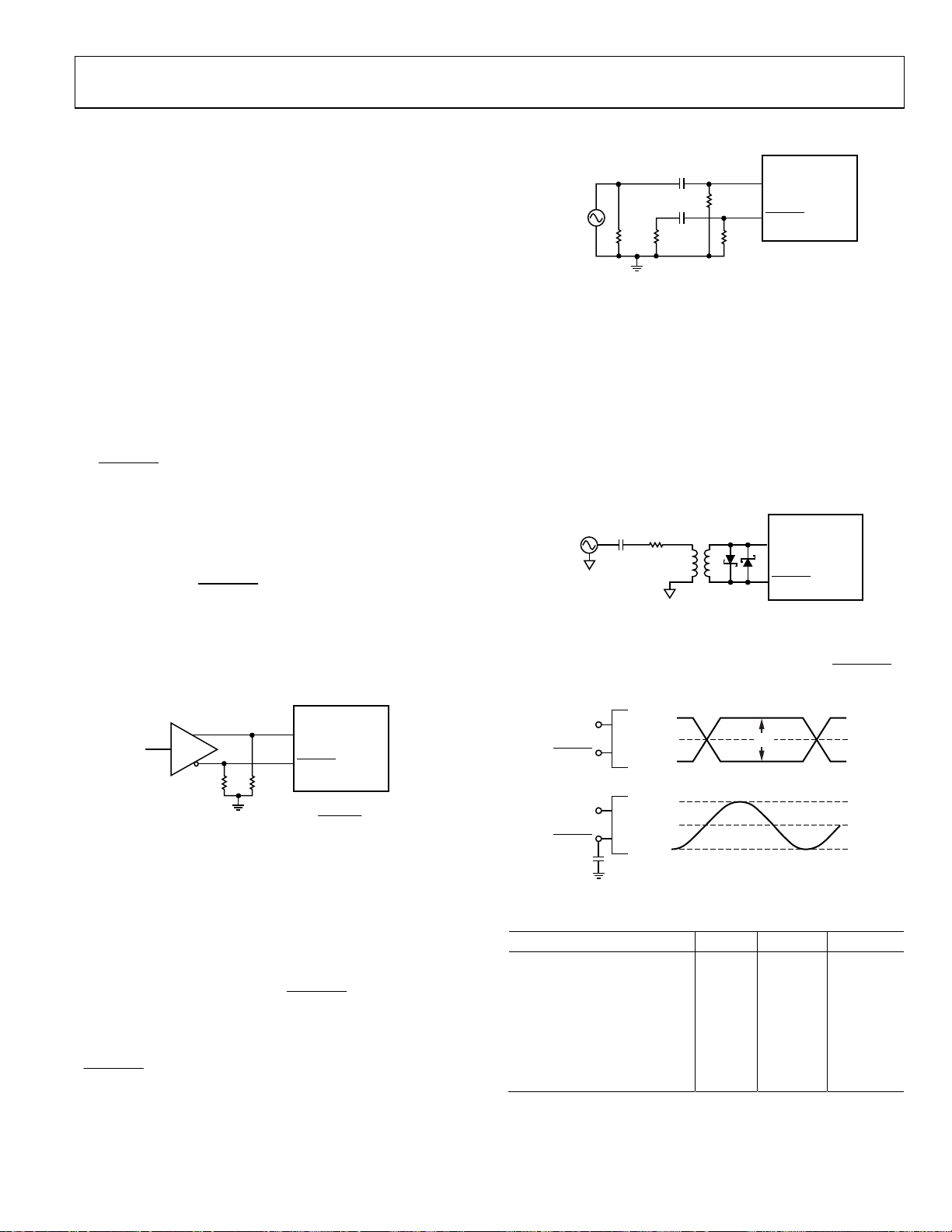
ENCODE INPUT
Any high speed ADC is extremely sensitive to the quality of the
sampling clock provided by the user. A track-and-hold circuit is
essentially a mixer, and any noise, distortion, or timing jitter on
the clock is combined with the desired signal at the ADC output.
For this reason, considerable care has been taken in the design
of the encode input of the AD9433, and the user is advised to
give commensurate thought to the clock source.
The AD9433 has an internal clock duty cycle stabilization
circuit that locks to the rising edge of ENCODE (falling edge
ENCODE
of
internally. This allows for a wide range of input duty cycles at
the input without degrading performance. Jitter in the rising
edge of the input is still of paramount concern and is not
reduced by the internal stabilization circuit. This circuit is
always on and cannot be disabled by the user.
The ENCODE and
to 3.75 V (nominal) and support either differential or singleended signals. For best dynamic performance, a differential
signal is recommended. Good performance is obtained using
an MC10EL16 translator in the circuit to directly drive the
encode inputs (see ). Figure 41
Often, the cleanest clock source is a crystal oscillator producing
a pure, single-ended sine wave. In this configuration, or with
any roughly symmetrical, single-ended clock source, the signal
can be ac-coupled to the encode input. To minimize jitter, the
signal amplitude should be maximized within the input range
described in Ta ble 7 . The 12 k resistors to ground at each of
the inputs, in parallel with the internal bias resistors, set the
common-mode voltage to approximately 2.5 V, allowing the
maximum swing at the input. The
bypassed with a capacitor to ground to reduce noise. This ensures
that the internal bias voltage is centered on the encode signal.
For best dynamic performance, impedances at ENCODE and
ENCODE
if driven differentially) and optimizes timing
ENCODE
PECL
GATE
Figure 41. Using PECL to Drive the
inputs are internally biased
AD9433
ENCODE
ENCODE
510Ω510Ω
ENCODE
Inputs
ENCODE
input should be
should match.
1977-041
0.1µF
12kΩ
50Ω
SINE
SOURCE
Figure 42. Single-Ended Sine Source Encode Circuit
0.1µF
12kΩ25Ω50Ω
Figure 43 shows another preferred method for clocking the
AD9433. The clock source (low jitter) is converted from singleended to differential using an RF transformer. The back-to-back
Schottky diodes across the transformer secondary limit clock
excursions into the AD9433 to approximately 0.8 V p-p differential. This helps to prevent the large voltage swings of the clock
from feeding through to other portions of the AD9433 and limits
the noise presented to the encode inputs. A crystal clock oscillator can also be used to drive the RF transformer if an appropriate
limiting resistor (typically 100 Ω) is placed in series with the
primary.
0.1µF
100Ω
CLOCK
SOURCE
Figure 43. Transformer-Coupled Encode Circuit
T1-4T
HMS2812
DIODES
ENCODE VOLTAGE LEVEL DEFINITION
The voltage level definitions for driving ENCODE and
in single-ended and differential mode are shown in . Figure 44
V
, V
IHD
V
, V
ICM
ECM
V
ILD
V
IHS
V
, V
ICM
ECM
V
ILS
200 mV 750 mV 5.5 V
−0.5 V V
)
ILS
3.75 V
2.0 V 4.25 V
ENCODE
ENCODE
ENCODE
ENCODE
0.1µF
Figure 44. Differential and Single-Ended Input Levels
Table 7. Encode Inputs
Input Min Nominal Max
Differential Signal Amplitude
(V
)
ID
Input Voltage Range
, V
IHD
, V
ILD
IHS
(V
Internal Common-Mode Bias
)
(V
ICM
External Common-Mode Bias
(V
)
ECM
ENCODE
ENCODE
ENCODE
ENCODE
V
ID
AD9433
AD9433
01977-042
01977-043
ENCODE
01977-044
+ 0.5 V
CC
Rev. A | Page 17 of 20
Page 18

AD9433
A
ANALOG INPUT
The analog input to the AD9433 is a differential buffer. The
input buffer is self-biased by an on-chip resistor divider that
sets the dc common-mode voltage to a nominal 4 V (see the
Equivalent Circuits section). Rated performance is achieved
by driving the input differentially. The minimum input offset
voltage is obtained when driving from a source with a low
differential source impedance, such as a transformer in ac
applications (see Figure 45). Capacitive coupling at the inputs
increases the input offset voltage by as much as 50 mV.
AD9433
50Ω
NALOG
SIGNAL
SOURCE
Figure 45. Transformer-Coupled Analog Input Circuit
25Ω
25Ω
1:1
0.1µF
AIN
AIN
01977-045
In the highest frequency applications, two transformers connected in series may be necessary to minimize even-order
harmonic distortion. The first transformer isolates and converts
the signal to a differential signal, but the grounded input on the
primary side degrades amplitude balance on the secondary
winding. Capacitive coupling between the windings causes
this imbalance. Because one input to the first transformer is
grounded, there is little or no capacitive coupling, resulting in
an amplitude mismatch at the output of the first transformer. A
second transformer improves the amplitude balance, and thus
improves the harmonic distortion. A wideband transformer,
such as the ADT1-1WT from Mini-Circuits®, is recommended
for these applications, because the bandwidth through the two
transformers is reduced by √2.
AD9433
50Ω
ANALOG
SIGNAL
SOURCE
Figure 46. Driving the Analog Input with Two Transformers for Improved
Even-Order Harmonics
25Ω
25Ω
1:11:1
0.1µF
AIN
AIN
01977-046
Driving the ADC single-ended degrades performance, particularly even-order harmonics. For best dynamic performance,
impedances at AIN and
AIN
should match. Special care was
taken in the design of the analog input section of the AD9433
to prevent damage and corruption of data when the input is
overdriven.
SFDR OPTIMIZATION
When set to Logic 1, the SFDR MODE pin enables a proprietary
circuit that can improve the spurious-free dynamic range (SFDR)
performance of the AD9433. This pin is useful in applications
where the dynamic range of the system is limited by discrete
spurious frequency content caused by nonlinearities in the
ADC transfer function.
Rev. A | Page 18 of 20
Enabling this circuit gives the circuit a dynamic transfer functi
meaning that the voltage t
hreshold between two adjacent output
codes can change from clock cycle to clock cycle. While improving
spurious frequency content, this dynamic aspect of the transfer
function may be inappropriate for some time domain applications
of the converter. Connecting the SFDR MODE pin to ground
disables this function. The improvement in the linearity of the
converter and its effect on spurious free dynamic range is shown
in Figure 4 and Figure 5 and in Figure 22 and Figure 23.
DIGITAL OUTPUTS
The digital outputs are 3 V (2.7 V to 3.3 V) TTL-/CMOScompatible for lower pow
er consumption. The output data
format is selectable through the data format select (DFS)
CMOS input. DFS = 1 selects offset binary; DFS = 0 selects
twos complement coding (see Table 8 and Table 9).
Table 8. Offset Binary Output Coding (DFS = 1, V
AIN
Code
AIN −
(V)
Digital Output
REF
4095 +1.000 1111 1111 1111
… … …
2048 0 1000 0000 0000
2047 0049 1 1111 1111 −0.0 011
… … …
0 −1.000 0000 0000 0000
Table 9. Twos Comple nt Output C
FS = 0, V
(D
Code AIN −
=me 2.5 V)
REF
AIN
(V) Digital Output
oding
+2047 +1.000 0111 1111 1111
… … …
0 0 0000 0000 0000
−1 −0.00049 1 1111 1111 111
… … …
−2048 −1.000 1000 0000 0000
VOLTAGE RE ENCE
and acc V voltage refer he
A stable urate 2.5 ence is built into t
AD9433 (VREFOUT). In nor
FER
mal operation, the internal reference is used by strapping Pin 45 to Pin 46 and placing a 0.1 µF
decoupling capacitor at VREFIN. The input range can be adjusted
by varying the reference voltage applied to the AD9433. No appreciable degradation in performance occurs when the reference is
adjusted ±5%. The full-scale range of the ADC tracks reference
voltage changes linearly.
TIMING
The AD9433 provides latc
delays. Dat
a outputs are available one propagation delay (t
after the rising edge of the encode command (see Figure 2). T
length of the output data lines and the loads placed on them
should be minimized to reduce transients within the AD9433;
these transients can detract from the dynamic performance of
the converter. The minimum guaranteed conversion rate of the
AD9433 is 10 MSPS. At internal clock rates below 10 MSPS,
dynamic performance may degrade.
hed data outputs, with 10 pipeline
= 2.5
PD
on,
V)
)
he
Page 19

AD9433
APPLICATIONS INFORMATION
LAYOUT INFORMATION
A multilayer board is recommended to achieve best results. It is
highly recommended that high quality, ceramic chip capacitors be
used to decouple each supply pin to ground directly at the device.
The pinout of the AD9433 facilitates ease of use in the implementation of high frequency, high resolution design practices.
All of the digital outputs and their supply and ground pin
connections are segregated on one side of the package, with
the inputs on the opposite side for isolation purposes.
Care should be taken when routing the digital output traces.
To prevent coupling through the digital outputs into the analog
portion of the AD9433 (V
loading should be placed on these outputs.
It is recommended that a fanout of only one gate be used for all
AD9433 digital outputs.
The layout of the encode circuit is equally critical and should be
treated as an analog input. Any noise received on this circuitry
results in corruption in the digitization process and lower overall performance. The encode clock must be isolated from the
digital outputs and the analog inputs.
, AIN, and VREF), minimal capacitive
CC
REPLACING THE AD9432 WITH THE AD9433
The AD9433 is pin-compatible with the AD9432, although there
are two control pins on the AD9433 that are do not connect (DNC)
and supply (V
Table 10. AD9432/AD9433 Pin Differences
Pin AD9432 AD9433
41 DNC DFS
42 VCC SFDR MODE
Using the AD9433 in an AD9432 pin assignment configures the
AD9433 as follows:
• The SFDR improvement circuit is enabled.
• The DFS pin floats low, selecting twos complement coding
for the digital outputs. (Twos complement coding is the
only output coding available on the AD9432.)
Table 11 summarizes the differences between the AD9432 and
AD9433 analog and encode input common-mode voltages.
These inputs can be ac-coupled so that the devices can be used
interchangeably.
Table 11. AD9432/AD9433 Analog and Encode Input
Common-Mode Voltages
Input Pins
ENCODE/ENCODE
AIN/AIN
) connections on the AD9432 (see Table 10).
CC
Common-Mode Voltage
AD9432 AD9433
1.6 V 3.75 V
3.0 V 4.0 V
Rev. A | Page 19 of 20
Page 20

AD9433
OUTLINE DIMENSIONS
0.75
0.60
0.45
SEATING
PLANE
VIEW A
0° MIN
0.20
0.09
3.5°
0.08 MAX
COPLANARIT Y
1.05
1.00
0.95
0.15
0.05
ROTATED 90° CCW
1.20
MAX
1
7°
0°
13
Figure 47. 52-Lead Thin Quad
12.00 BSC
SQ
52
PIN 1
TOP VI
(PINS DOWNEW)
14
VIEW A
COMPLIANT TO JEDEC STANDARDS
40
39
27
26
Flat Pack
40
39
10.00
B QSC S
27
MS-026-ACC
BOTTOM VIEW
26
0.65
BSC
LEAD PITCH
EXPO
PA
(PINS UP)
age, Exposed Pad [TQFP_EP]
SED
D
52
1
7.30 B
SQ
13
14
0.38
0.32
FOR PROPER CONNECTION O F
0.22
THE EXPOSED PAD, REFER TO
THE PIN CONF IGURATIO N AND
FUNCTION DES CRIPTIONS
SECTION O F THIS DAT A SHEET.
SC
072508-A
(SV-52-2)
Dimensions sho
wn in
millimeters
ORDERING GUIDE
Model Temperature Range Package Description Package Option
AD9433BSVZ-105
AD9433BSVZ-125
1
Z = RoHS Compliant Part.
1
−40°C to +85°C 52-Lead Thin Quad Flat Package, Exposed Pad [TQFP_EP] SV-52-2
1
−40°C to +85°C 52-Lead Thin Quad Flat Pa ed Pad [TQFP_ Sckage, Expos EP] V-52-2
©2001–2009 Analog Devices, Inc. All rights reserved. Trademarks and
registered trademarks are the property of their respective owners.
D01977-0-6/09(A)
Rev. A | Page 20 of 20
 Loading...