

Page 1

10-Bit Integrated, Multiformat, HDTV Video Decoder,
www.BDTIC.com/IC
RGB Graphics Digitizer, and 2:1 Multiplexed
HDMI/DVI Interface
FEATURES
Mutliformat decoder
Three 10-bit analog-to-digital converters (ADCs)
ADC sampling rates up to 170 MHz
Mux with 12 analog input channels
525i-/625i-component SD support
525p-/625p-component progressive scan support
720p-/1080i-/1080p-component HDTV support
Digitizes RGB graphics up to 1600 × 1200 at 60 Hz (UXGA)
VBI data slicer (including teletext)
Analog-to-HDMI fast switching
Dual High-Definition Multimedia Interface (HDMI) Rx
2:1 multiplexed HDMI receiver
HDMI 1.3, DVI 1.0
225 MHz HDMI receiver
Repeater support
High-bandwidth digital content protection (HDCP 1.3)
36-bit deep color support
S/PDIF (IEC60958-compatible) digital audio output
Multichannel I
Adaptive equalizer for cable lengths up to 30 meters
Internal EDID RAM
General
Highly flexible output interface
STDI function support standard identification
2 any-to-any 3 × 3 color-space conversion matrices
Programmable interrupt request output pins
APPLICATIONS
Advanced TVs
PDP HDTVs
LCD TVs (HDTV ready)
LCD/DLP® rear projection HDTVs
CRT HDTVs
LCoS® HDTVs
Audio/video receivers (AVRs)
LCD/DLP front projectors
HDTV STBs with PVR
DVD recorders with progressive scan input support
2
S audio output (up to 8 channels)
AD9388A
GENERAL DESCRIPTION
The AD9388A is a high quality, single-chip graphics digitizer
with an integrated 2:1 multiplexed HDMI™ receiver.
The AD9388A contains one main component processor (CP)
that processes YPrPb and RGB component formats, including
RGB graphics. The CP also processes the video signals from the
HDMI receiver. The AD9388A can keep the HDCP link between
an HDMI source and the selected HDMI port active in analog
mode operation. This allows for fast switching between the
analog and HDMI modes.
The AD9388A supports the decoding of a component RGB or
YPrPb video signal into a digital YCrCb or RGB pixel output
stream. The support for component video includes 525i, 625i,
525p, 625p, 720p, 1080i, 1080p, and 1250i standards, as well as
many other HD and SMPTE standards.
Graphic digitization is also supported by the AD9388A. The
AD9388A is capable of digitizing RGB graphics signals from
VGA to UXGA rates and converting them into a digital RGB
or YCrCb pixel output stream.
The AD9388A incorporates a dual input, HDMI 1.3-compatible
receiver that supports HDTV formats up to 1080p and display
resolutions up to UXGA (1600 × 1200 at 60 Hz). The reception
of encrypted video is possible with the inclusion of HDCP. In
addition, the inclusion of adaptive equalization ensures robust
operation of the interface with cable lengths up to 30 meters. The
HDMI receiver has an advanced audio functionality, such as a
mute controller that prevents audible extraneous noise in the
audio output.
Derivative parts of the AD9388A are available; AD9388ABSTZA5 is composed of one analog and one digital input. To facilitate professional applications, where HDCP processing and
decryption are not required, the AD9388ABSTZ-5P derivative
is available. This allows users who are not HDCP adopters to
purchase the AD9388A. See the Ordering Guide for details on
these derivative parts.
Fabricated in an advanced CMOS process, the AD9388A is
available in a space saving, 144-lead, surface-mount, RoHScompliant, plastic LQFP and is specified over the −40°C to
+85°C temperature range.
B
Rev.
Information furnished by Analog Devices is believed to be accurate and reliable. However, no
responsibility is assumed by Anal og Devices for its use, nor for any infringements of p atents or other
rights of third parties that may result from its use. Specifications subject to chan ge without notice. No
license is granted by implication or otherwise under any patent or patent rights of Analog Devices.
Trademarks and registered trademarks are the property of their respective owners.
One Technology Way, P.O. Box 9106, Norwood, MA 02062-9106, U.S.A.
Tel: 781.329.4700
Fax: 781.461.3113 ©2007–2008 Analog Devices, Inc. All rights reserved.
www.analog.com
Page 2

AD9388A
www.BDTIC.com/IC
TABLE OF CONTENTS
Features .............................................................................................. 1
Applications ....................................................................................... 1
General Description ......................................................................... 1
Revision History ............................................................................... 2
Functional Block Diagram .............................................................. 3
Specifications ..................................................................................... 4
Electrical Characteristics ............................................................. 4
Analog and HDMI Specifications .............................................. 6
Data and I2C Timing Characteristics ......................................... 7
Absolute Maximum Ratings ............................................................ 9
Thermal Resistance ...................................................................... 9
Package Thermal Performance ................................................... 9
ESD Caution .................................................................................. 9
Pin Configurations and Function Descriptions ......................... 10
Functional Overview ...................................................................... 16
Analog Front End ....................................................................... 16
HDMI Receiver ........................................................................... 16
Component Processor Pixel Data Output Modes .................. 16
Component Video Processing .................................................. 16
RGB Graphics Processing ......................................................... 16
General Features ......................................................................... 16
Theory of Operation ...................................................................... 17
Analog Front End ....................................................................... 17
HDMI Receiver ........................................................................... 17
Component Processor (CP) ...................................................... 17
VBI Data Processor .................................................................... 17
Pixel Output Formatting................................................................ 18
Register Map Architecture ........................................................ 21
Typical Connection Diagram ................................................... 22
Recommended External Loop Filter Components ................ 23
AD9388A/ADV7441A Evaluation Platform .............................. 24
Outline Dimensions ....................................................................... 25
Ordering Guide .......................................................................... 25
REVISION HISTORY
7/08—Rev. SpA to Rev. B
5/08—Rev. Sp0 to Rev. SpA
Changes to General Description .................................................... 1
Added Figure 6 ................................................................................ 13
Added Table 7 .................................................................................. 13
Changes to Component Processor Pixel Data Output Modes
Section .............................................................................................. 16
Changes to Component Processor (CP) Section........................ 17
Added AD9388A/ADV7441A Evaluation Platform Section .... 24
Changes to Ordering Guide .......................................................... 25
10/07—Revsion Sp0: Initial Version
Rev. B | Page 2 of 28
Page 3
AD9388A
A
A
www.BDTIC.com/IC
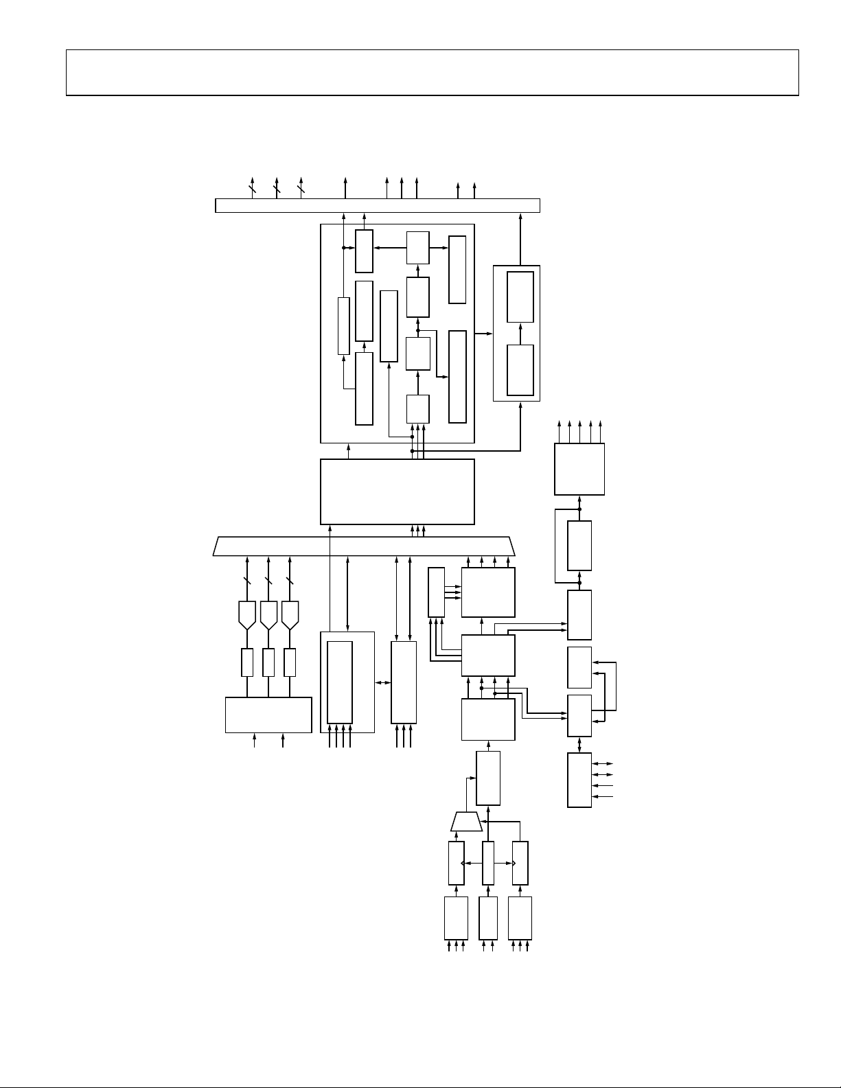
FUNCTIONAL BLOCK DIAGRAM
06915-001
P0 TO
P910P10 TO
P1910P20 TO
P29
PIXEL
DATA
10
INT1
SYNC EXTRACT
COMPONENT PRO CESSOR
DIGI TAL PROCESSI NG BLOCK
AD9388A
EMBEDDED
DATA
PREPROCESSOR
HS/CS
VS/FIELD
DE/FIELD
LLC
SYNC_OUT/
INT2
OUTPUT FORMATTER
DATA
ADDER
AV CODE
INSERTION
STANDARD
IDENTIFICATION
POLARITY DETECT
SYNC SOURCE AND
SYNC
OFFSET
HSYNC DEPTH
ACTIVE PEAK AND
GAIN
CONTROL
CGMS DETECT ION
MACROVISION AND
FINE
CLAMP
DIGITAL
PROG.
(A)
CONVERTER
COLOR SPACE
(A)
NOISE AND C ALIBRATI ON
DELAY
(B)
(C)
AND
FILTERS
DECIMATION
DOWNSAM PLING
(B)
(C)
ANCILLARY
DATA
ANCILLARY
FORMATTER
VBI DATA PROCESSOR
VBI
DECODER
S
2
LRCLK
SCLK
MCLKOUT
SPDIF
I
AUDIO
PROCESSING
ANALOG I NTERFACE
101010
ADC0
CLAMP
RGB
MUX
4:4:4
4:2:2 TO
CONVERSION
XOR
DEVSHS
HDMI
DECODE
DATA
RECOVERY
ALIGNM ENT
MUX
SAMPLEREQUALIZER
SAMPLER
MUX PLL
EQUALIZER
SCL
FILTER
CONTROL
C
2
I
CONTROL INTERFACE
SDA
ALSB
HS/CS, VS
ADC1
ADC2
CLAMP
CLAMP
INPUT
MATRIX
YPrPb
CONTROL
CONTROL AND DATA
LLC GENERATI ON
CLOCK GENER ATION
SYNC PROCESSING AND
SOY
SOG
VS_IN
HS_IN/C S_IN
PACKET/
MEMORY
INFOFRAME
PACKET
PROCESSOR
HDCP
HDCP
EDID/
REPEATER
EEPROM
ENGINE
CONTROLLER
MCL
MDA
DDCB_SCL
DDCB_SD
DDCA_SD
DDCA_SCL
RXA_0
RXA_1
RXA_2
RXB_0
RXB_1
RXA_C
RXB_2
RXB_C
Figure 1.
Rev. B | Page 3 of 28
Page 4

AD9388A
www.BDTIC.com/IC
SPECIFICATIONS
ELECTRICAL CHARACTERISTICS
AVDD = 1.71 V to 1.89 V, DVDD = 1.62 V to 1.98 V, DVDDIO = 2.97 V to 3.63 V, PVDD = 1.71 V to 1.89 V, TVDD = 3.135 V to
3.465 V, CVDD = 1.71 V to 1.89 V. Operating temperature range is −40°C to +85°C, unless otherwise noted.
Table 1.
Parameter
STATIC PERFORMANCE
Resolution (Each ADC) N 10 Bits
Integral Nonlinearity INL BSL at 27 MHz (@ a 10-bit level) –0.5/+2 –4/+6 LSB
BSL at 54 MHz (@ a 10-bit level) –0.5/+2 LSB
BSL at 74 MHz (@ a 10-bit level) –0.5/+1.5 LSB
BSL at 110 MHz (@ a 10-bit level) –0.7/+2 LSB
BSL at 170 MHz (@ an 8-bit level) –0.25/+0.5 LSB
Differential Nonlinearity DNL At 27 MHz (@ a 10-bit level) –0.5/+0.5 –0.95/+2 LSB
At 54 MHz (@ a 10-bit level) ±0.5 LSB
At 74 MHz (@ a 10-bit level) ±0.5 LSB
At 110 MHz (@ a 10-bit level) ±0.5 LSB
At 170 MHz (@ an 8-bit level) –0.25/+0.2 LSB
DIGITAL INPUTS
Input High Voltage
HS_IN, VS_IN low trigger mode 0.7 V
Input Low Voltage
HS_IN, VS_IN low trigger mode 0.3 V
Input Current IIN
All input pins other than Pin 21 –10 +10 μA
Input Capacitance
DIGITAL OUTPUTS
Output High Voltage
Output Low Voltage
High Impedance Leakage Current I
Output Capacitance
POWER REQUIREMENTS
Digital Core Power Supply DVDD 1.62 1.8 1.98 V
Digital I/O Power Supply DVDDIO 2.97 3.3 3.63 V
PLL Power Supply PVDD 1.71 1.8 1.89 V
Analog Power Supply AVDD 1.71 1.8 1.89 V
Terminator Power Supply TVDD 3.135 3.3 3.465 V
Comparator Power Supply CVDD 1.71 1.8 1.89 V
Digital Core Supply Current I
YPrPb 1080p sampling @ 148.5 MHz
HDMI RGB sampling @ 165 MHz
HDMI RGB sampling @ 225 MHz
Digital I/O Supply Current I
YPrPb 1080p sampling @ 148.5 MHz
HDMI RGB sampling @ 165 MHz
HDMI RGB sampling @ 225 MHz
HDMI Comparators I
1
2
3
3
4
5
5
V
4
C
4
Symbol Test Conditions Min Typ Max Unit
VIH 2 V
VIL 0.8 V
Pin 21 (RESET
)
–60 +60 μA
CIN 10 pF
VOH I
I
OL
10 μA
LEAK
20 pF
OUT
Graphics RGB sampling @ 108 MHz6 141 252 mA
DVDD
Graphics RGB sampling @ 108 MHz
DVDDIO
Graphics RGB sampling @ 108 MHz
CVDD
= 0.4 mA 2.4 V
SOURCE
= 3.2 mA 0.4 V
SINK
6
203 263 mA
7, 8
242 329 mA
7, 8
242 326 mA
6
17 37 mA
6
42 62 mA
7, 8
17 34 mA
7, 8
20 34 mA
6
56 78 mA
Rev. B | Page 4 of 28
Page 5
AD9388A
www.BDTIC.com/IC
Parameter
TMDS PLL and Equalizer
1
Symbol Test Conditions Min Typ Max Unit
6
YPrPb 1080p sampling @ 148.5 MHz
56 79 mA
Supply Current
7, 8
HDMI RGB sampling @ 165 MHz
HDMI RGB sampling @ 225 MHz
Analog Supply Current I
Graphics RGB sampling @ 108 MHz
AVDD
YPrPb 1080p sampling @ 148.5 MHz
HDMI RGB sampling @ 165 MHz
HDMI RGB sampling @ 225 MHz
Terminator Supply Current I
Graphics RGB sampling @ 108 MHz
TVDD
YPrPb 1080p sampling @ 148.5 MHz
HDMI RGB sampling @ 165 MHz
HDMI RGB sampling @ 225 MHz
Audio and Video Supply Current I
Graphics RGB sampling @ 108 MHz
PVDD
YPrPb 1080p sampling @ 148.5 MHz
HDMI RGB sampling @ 165 MHz
HDMI RGB sampling @ 225 MHz
Power-Down Current I
Power-Up Time t
1
The minimum/maximum specifications are guaranteed over the −40°C to +85°C temperature range (T
2
All ADC linearity tests performed at input range of full scale − 12.5% and at zero scale + 12.5%.
3
Pin 1, Pin 105, Pin 106, and Pin 144 are 5 V tolerant.
4
Guaranteed by characterization.
5
VOH and VOL levels obtained using default drive strength value (0x15) in User Map Register 0xF4.
6
Current measurements for analog inputs were made with HDMI/analog simultaneous mode disabled (User Map Register 0xBA Bit 7 programmed with Value 0) and no
HDMI sources connected to the part.
7
Current measurements for HDMI inputs were made with a source connected to the active HDMI port and no source connected to the inactive HDMI port.
8
Audio stream is uncompressed stereo audio sampling frequency of fS = 48 kHz and MCLKOUT = 256 fS.
9
The terminator supply current may vary with the HDMI source in use.
11.6 mA
PWRDN
25 ms
PWRUP
86 105 mA
7, 8
95 118 mA
6
174 278 mA
6
180 284 mA
7, 8
0 2 mA
7, 8
0 2 mA
6
12 18 mA
6
12 18 mA
7, 8, 9
42 47 mA
7, 8, 9
63 69 mA
6
14 21 mA
6
19 24 mA
7, 8
10 19 mA
7, 8
15 20 mA
to T
MAX
).
MIN
Rev. B | Page 5 of 28
Page 6

AD9388A
www.BDTIC.com/IC
ANALOG AND HDMI SPECIFICATIONS
AVDD = 1.71 V to 1.89 V, DVDD = 1.62 V to 1.98 V, DVDDIO = 2.97 V to 3.63 V, PVDD = 1.71 V to 1.89 V, TVDD = 3.135 V to
3.465 V, CVDD = 1.71 V to 1.89 V. Operating temperature range is −40°C to +85°C, unless otherwise noted.
Table 2.
Parameter
ANALOG
Clamp Circuitry
HDMI SPECIFICATIONS
Intrapair (Positive-to-Negative) Differential Input Skew 0.4 t
Channel-to-Channel Differential Input Skew
1
The minimum/maximum specifications are guaranteed over the −40°C to +85°C temperature range.
2
Guaranteed by characterization.
3
Guaranteed by design.
4
t
is 1/10 the pixel period of the TMDS clock.
bit
5
t
pixel
1, 2
Test Conditions Min Typ Max Unit
External Clamp Capacitor 0.1 μF
Input Impedance (Except Pin 74) Clamps switched off 10 MΩ
Input Impedance of Pin 74 20 kΩ
CML 0.88 V
ADC Full-Scale Level CML + 0.5 V
ADC Zero-Scale Level CML − 0.5 V
ADC Dynamic Range 1 V
Clamp Level (When Locked) Component input (Y signal) CML − 0.120 V
Component input (Pr signal) CML V
Component input (Pb signal) CML V
PC RGB input (R, G, B signals) CML − 0.120 V
3
is the period of the TMDS clock.
4
bit
5
0.2 t
+ 1.78 ns
pixel
Rev. B | Page 6 of 28
Page 7

AD9388A
www.BDTIC.com/IC
DATA AND I2C TIMING CHARACTERISTICS
AVDD = 1.71 V to 1.89 V, DVDD = 1.62 V to 1.98 V, DVDDIO = 2.97 V to 3.63 V, PVDD = 1.71 V to 1.89 V, TVDD = 3.135 V to
3.465 V, CVDD = 1.71 V to 1.89 V; operating temperature range is −40°C to +85°C, unless otherwise noted.
Table 3.
1, 2
Parameter
Symbol Test Conditions Min Typ Max Unit
SYSTEM CLOCK AND CRYSTAL
Crystal Nominal Frequency 28.6363 MHz
Crystal Frequency Stability ±50 ppm
Horizontal Sync Input Frequency 14.8 110 kHz
LLC Frequency Range 12.825 170 MHz
3
I2C PORTS (FAST MODE)
xCL Frequency
xCL Minimum Pulse Width High
xCL Minimum Pulse Width Low
4
4
t
4
t
400 kHz
0.6 μs
1
1.3 μs
2
Hold Time (Start Condition) t3 0.6 μs
Setup Time (Start Condition) t4 0.6 μs
xDA Setup Time
xCL and xDA Rise Times
xCL and xDA Fall Times
4
t
4
t
4
t
100 ns
5
300 ns
6
300 ns
7
Setup Time (Stop Condition) t8 0.6 μs
I2C PORTS (NORMAL MODE)
xCL Frequency 100 kHz
xCL Minimum Pulse Width High t1 4 μs
xCL Minimum Pulse Width Low t2 4.7 μs
Hold Time (Start Condition) t3 4 μs
Setup Time (Start Condition) t4 4.7 μs
xDA Setup Time t5 250 ns
xCL and xDA Rise Times t6 1000 ns
xCL and xDA Fall Times t7 300 ns
Setup Time (Stop Condition) t8 4 μs
RESET FEATURE
Reset Pulse Width 5 ms
CLOCK OUTPUTS
LLC Mark Space Ratio t9:t10 45:55 55:45
% duty
cycle
DATA AND CONTROL OUTPUTS
Data Output Transition Time SDR (CP)
t
5
t11 End of valid data to negative clock edge 2 ns
Negative clock edge to start of valid data 0.5 ns
12
I2S PORT (MASTER MODE)
SCLK Mark Space Ratio t13:t14
45:55 55:45
% duty
cycle
LRCLK Data Transition Time t15
LRCLK Data Transition Time t16
I2Sx Data Transition Time
I2Sx Data Transition Time
MCLKOUT Frequency
1
The minimum/maximum specifications are guaranteed over the −40°C to +85°C temperature range (T
2
Guaranteed by characterization.
3
Refers to all I2C pins (DDC and control port).
4
The prefix x refers to pin names beginning with S, DDCA_S, and DDCB_S.
5
CP timing figures were obtained using the maximum drive strength value (0x3F) in User Map Register 0xF4.
6
The suffix x refers to pin names ending with 0, 1, 2, and 3.
6
6
t
t
17
18
4.096 24.576 MHz
End of valid data to negative SCLK edge 10 ns
Negative SCLK edge to start of valid data 10 ns
End of valid data to negative SCLK edge 5 ns
Negative SCLK edge to start of valid data 5 ns
to T
MAX
).
MIN
Rev. B | Page 7 of 28
Page 8
AD9388A
www.BDTIC.com/IC
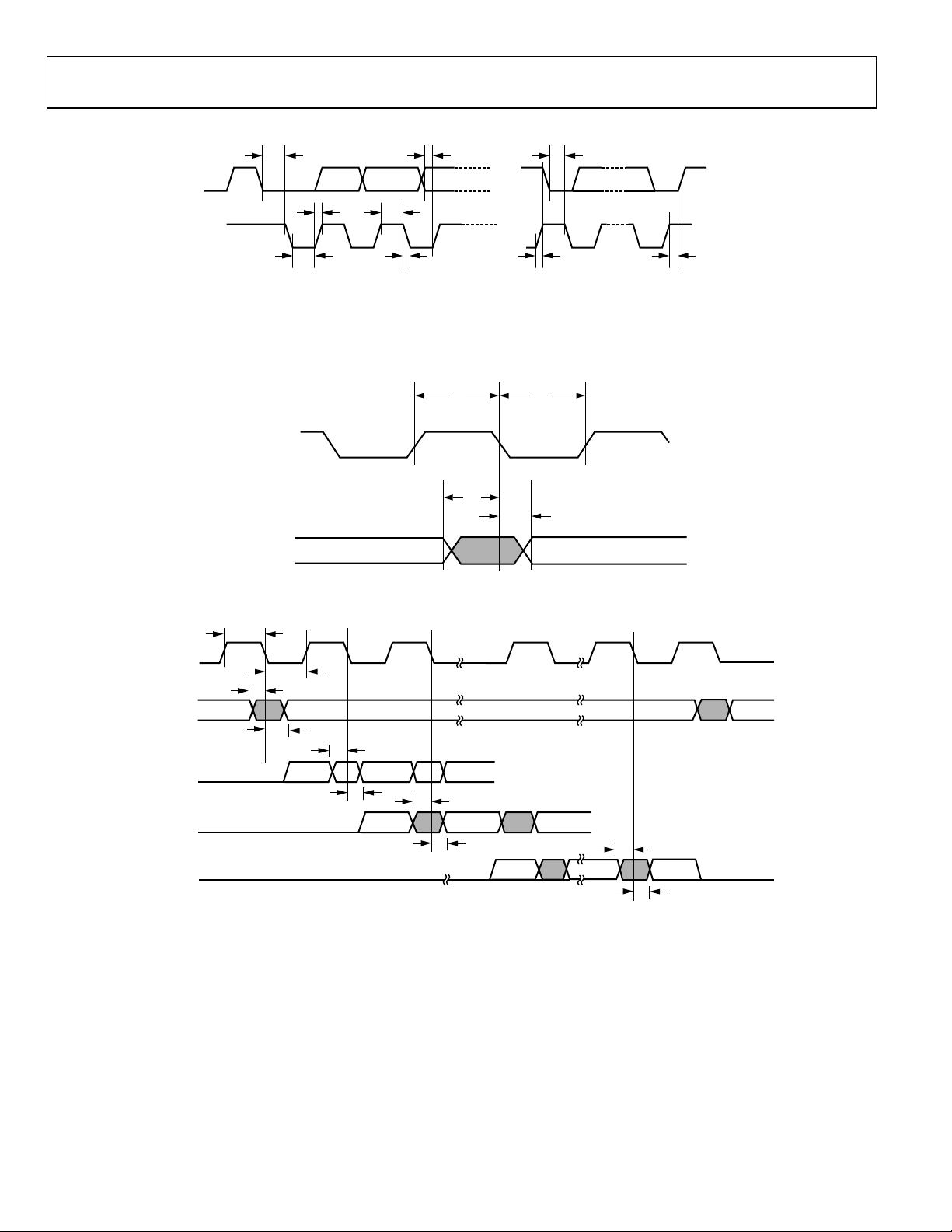
Timing Diagrams
t
3
xDA
t
t
6
1
xCL
t
2
NOTES
1. THE PREF IX x REFERS TO PIN NAMES BEGINNING WITH S, DDCA_S, AND DDCB_S.
t
7
Figure 2. I
t
5
2
C Timing
t
3
t
4
t
8
06915-002
LLC
P0 TO P29, VS,
HS, FIEL D/DE
t
9
t
11
t
10
t
12
06915-004
Figure 3. Pixel Port and Control CP Output Timing (CP Core)
t
13
SCLK
t
14
t
15
LRCLK
t
16
t
LEFT-JUSTIFIED
RIGHT -JUSTI FIED
I2Sx
MODE
I2Sx
2
I
S MODE
I2Sx
MODE
NOTES
1. THE SUF FIX x REFE RS TO PI N NAMES ENDING W ITH 0, 1, 2, AND 3.
17
MSB MSB – 1
t
18
MSB
t
17
t
18
Figure 4. I
MSB – 1
2
S Timing
t
17
LSBMSB
t
18
06915-005
Rev. B | Page 8 of 28
Page 9
AD9388A
www.BDTIC.com/IC
ABSOLUTE MAXIMUM RATINGS
Table 4.
Parameter Rating
AVDD to AGND 2.2 V
DVDD to DGND 2.2 V
PVDD to PGND 2.2 V
DVDDIO to DGND 4 V
CVDD to CGND 2.2 V
TVDD to TGND 4 V
DVDDIO to AVDD −0.3 V to +3.6 V
DVDDIO to TVDD −3.6 V to +3.6 V
DVDDIO to DVDD −2 V to +2 V
CVDD to DVDD −2 V to +0.3 V
PVDD to DVDD −2 V to +0.3 V
AVDD to CVDD −2 V to +2 V
AVDD to PVDD −2 V to +2 V
AVDD to DVDD −2 V to +2 V
AVDD to TVDD −3.6 V to +0.3 V
TVDD to DVDD −2 V to +2 V
Digital Inputs
Voltage to DGND DGND − 0.3 V to DVDDIO + 0.3 V
Digital Outputs
Voltage to DGND
Analog Inputs
Voltage to AGND
Maximum Junction
Temperature (T
Storage Temperature Range −65°C to +150°C
Infrared Reflow,
Soldering (20 sec)
) 125°C
J_MAX
DGND − 0.3 V to DVDDIO + 0.3 V
AGND − 0.3 V to AVDD + 0.3 V
260°C
Stresses above those listed under Absolute Maximum Ratings
may cause permanent damage to the device. This is a stress
rating only; functional operation of the device at these or any
other conditions above those indicated in the operational
section of this specification is not implied. Exposure to absolute
maximum rating conditions for extended periods may affect
device reliability.
THERMAL RESISTANCE
Table 5.
Package Type Ψ
144-Lead LQFP (ST-144) 1.62 °C/W
1
Junction-to-package surface thermal resistance.
1
Unit
JT
PACKAGE THERMAL PERFORMANCE
To reduce power consumption during AD9388A operation,
turn off unused ADCs.
On a four-layer PCB that includes a solid ground plane, the θ
JA
value is 25.3°C/W. However, due to variations within the PCB
metal and, therefore, variations in PCB heat conductivity, the
value of θ
may differ for various PCBs.
JA
The most efficient measurement technique is to use the surface
temperature of the package to estimate the die temperature
because this is not affected by the variance associated with the
θ
value.
JA
The maximum junction temperature (T
) of 125°C must not
J_MAX
be exceeded. The following equation calculates the junction
temperature using the measured surface temperature of the
package and applies only when no heat sink is used on DUT:
T
= TS + (ΨJT × W
J_MAX
TOTAL
)
where:
T
is the surface temperature of the package expressed in
S
degrees Celsius.
Ψ
is the junction-to-package surface thermal resistance.
JT
W
= {(AV D D × IAVDD) + (DVDD × IDVDD) + (DVDDIO
TOTAL
× IDVDDIO) + (PVDD × IPVDD) + (CVDD × ICVDD) +
(TVDD × ITVDD)}.
Contact an Analog Devices, Inc., representative for more details
on package thermal performance at video.products@analog.com.
ESD CAUTION
Rev. B | Page 9 of 28
Page 10

AD9388A
www.BDTIC.com/IC
PIN CONFIGURATIONS AND FUNCTION DESCRIPTIONS
CVDD
CGND
TVDD
RXA_CN
RXA_CP
TGND
RXA_0N
RXA_0P
TGND
RXA_1N
RXA_1P
TGND
RXA_2N
RXA_2P
TVDD
RTERM
CVDD
CGND
TVDD
RXB_CN
RXB_CP
TGND
RXB_0N
RXB_0P
TGND
RXB_1N
RXB_1P
TGND
RXB_2N
RXB_2P
TVDD
CGND
CVDD
DVDD
DGND
DDCB_SCL
109
110
111
112
113
114
115
116
117
118
119
120
121
122
123
124
125
126
127
128
129
130
131
132
133
134
135
136
137
138
139
140
141
142
143
144
DDCB_SDA
SPDIF
I2S0
I2S1
I2S2
I2S3
LRCLK
SCLK
MCLKOUT
EXT_CLAMP
SDA
SCL
ALSB
DGND
DVDDIO
DE/FIELD
HS/CS
VS/FIELD
SYNC_OUT/INT2
INT1
RESET
DGND
DVDD
DGND
DVDDIO
P10
1
PIN 1
2
3
4
5
6
7
8
9
10
11
12
13
14
15
16
17
18
19
20
21
22
23
24
P0
25
P1
26
P2
27
P3
28
P4
29
P5
30
P6
31
P7
32
P8
33
P9
34
35
36
37
48
49
50
AD9388A
TOP VIEW
(Not to Scale)
51
52
56
57
58
62
63
64
65
66
67
68
69
108
TEST5
107
TEST4
106
DDCA_SDA
105
DDCA_SCL
104
CVDD
103
CGND
102
AUDIO_ELPF
101
PVDD
100
PGND
99
AIN6
98
AIN12
97
SOY
96
AIN5
95
AIN11
94
AIN4
93
AIN10
92
REFP
91
TEST3
90
REFN
89
TEST2
88
AVDD
87
AGND
86
CML
85
REFOUT
84
AVDD
83
AGND
82
AGND
81
AIN3
80
AIN9
79
AIN2
78
AIN8
77
AIN1
76
AIN7
75
SOG
74
TEST1
73
TEST0
70
71
72
P1138P1239P1340P1441P1542P1643P1744P1845P1946P2047P21
EXT_CLK
DGND
DVDDIO
P2253P2354P2455P25
LLC
DGND
P2659P2760P2861P29
DVDD
DGND
XTAL
XTAL1
VS_IN
HS_IN/CS_IN
ELPF
PVDD
PVDD
PGND
DVDDIO
PGND
06915-006
Figure 5. Pin Configuration
Table 6. Pin Function Descriptions
Pin No. Mnemonic Type1Description
14, 22, 34, 49, 56, 64, 143 DGND G Digital Ground.
82, 83, 87 AGND G Analog Ground.
69, 72, 100 PGND G PLL Ground.
103, 110, 126, 140 CGND G Comparator Ground.
114, 117, 120, 130, 133, 136 TGND G Terminator Ground.
15, 35, 50, 67 DVDDIO P Digital I/O Supply Voltage (3.3 V).
23, 57, 142 DVDD P Digital Core Supply Voltage (1.8 V).
84, 88 AVDD P Analog Supply Voltage (1.8 V).
68, 71, 101 PVDD P Audio and Video PLL Supply Voltage (1.8 V).
104, 109, 125, 141 CVDD P HDMI Comparator, TMDS PLL, and Equalizer Supply Voltage (1.8 V).
111, 123, 127, 139 TVDD P Terminator Supply Voltage (3.3 V).
73, 74, 91, 108 TEST0, TEST1, TEST3, TEST5 I Test Pins. Do not connect.
89 TEST2 O Test Pin. Do not connect.
107 TEST4 I/O Test Pin. Do not connect.
76 to 81, 93 to 96, 98, 99 AIN1 to AIN12 I Analog Video Input Channel.
Rev. B | Page 10 of 28
Page 11

AD9388A
www.BDTIC.com/IC
Pin No. Mnemonic Type1Description
24 to 33, 36 to 47, 52 to 55,
58 to 61
19 INT1 O
20 SYNC_OUT/INT2 O Sliced Synchronization Output Signal (SYNC_OUT).
Interrupt Signal (INT2).
17 HS/CS O Horizontal Synchronization Output Signal (HS).
18 VS/FIELD O Vertical Synchronization Output Signal (VS).
16 DE/FIELD O Data Enable Signal (DE). Indicates active pixel data.
11 SDA I/O
12 SCL I
13 ALSB I This pin sets the second LSB of each AD9388A register map.
21
51 LLC O Line-Locked Output Clock for Pixel Data. Range is 13.5 MHz to 170 MHz.
65 XTAL1 O
66 XTAL I
70 ELPF O
102 AUDIO_ELPF O
85 REFOUT O Internal Voltage Reference Output.
86 CML O Common-Mode Level for the Internal ADCs.
90 REFN I Internal Voltage Output.
92 REFP I Internal Voltage Output.
63 HS_IN/CS_IN I
62 VS_IN I
75 SOG I
97 SOY I
112 RXA_CN I Digital Input Clock Complement of Port A in the HDMI Interface.
113 RXA_CP I Digital Input Clock True of Port A in the HDMI Interface.
115 RXA_0N I Digital Input Channel 0 Complement of Port A in the HDMI Interface.
116 RXA_0P I Digital Input Channel 0 True of Port A in the HDMI Interface.
118 RXA_1N I Digital Input Channel 1 Complement of Port A in the HDMI Interface.
119 RXA_1P I Digital Input Channel 1 True of Port A in the HDMI Interface.
P0 to P29 O Video Pixel Output Port.
Interrupt. Can be active low or active high. The set of events that
triggers an interrupt is under user control.
Composite Synchronization (CS). A single signal containing both
horizontal and vertical synchronization pulses.
Field Synchronization (FIELD). Field synchronization output signal in
all interlaced video modes.
Field Synchronization (FIELD). Field synchronization output signal in
all interlaced video modes.
2
C Port Serial Data Input/Output Pin. SDA is the data line for the
I
control port.
2
C Port Serial Clock Input. (Maximum clock rate of 400 kHz.) SCL is
I
the clock line for the control port.
RESET
I
System Reset Input. Active low. A minimum low reset pulse width of
5 ms is required to reset the AD9388A circuitry.
This pin should be connected to the 28.63636 MHz crystal or left as a
no connect if an external 3.3 V 28.63636 MHz clock oscillator source is
used to clock the AD9388A. In crystal mode, the crystal must be a
fundamental crystal.
Input Pin for the 28.63636 MHz Crystal. This pin can be overdriven by
an external 3.3 V 28.63636 MHz clock oscillator source to clock the
AD9388A.
The recommended external loop filter must be connected to this
ELPF pin.
The recommended external loop filter must be connected to this
AUDIO_ELPF pin.
HS Input Signal. Used in analog mode for 5-wire timing mode.
CS Input Signal. Used in analog mode for 4-wire timing mode.
For optimal performance, a 100 Ω series resistor is recommended on
the HS_IN/CS_IN pin.
VS Input Signal. This pin is used in analog mode for 5-wire timing
mode. For optimal performance, a 100 Ω series resistor is
recommended on the VS_IN pin.
Synchronization-on-Green Input. This pin is used in embedded
synchronization mode.
Synchronization-on-Luma Input. This pin is used in embedded
synchronization mode.
Rev. B | Page 11 of 28
Page 12

AD9388A
www.BDTIC.com/IC
Pin No. Mnemonic Type1Description
121 RXA_2N I Digital Input Channel 2 Complement of Port A in the HDMI Interface.
122 RXA_2P I Digital Input Channel 2 True of Port A in the HDMI Interface.
128 RXB_CN I Digital Input Clock Complement of Port B in the HDMI Interface.
129 RXB_CP I Digital Input Clock True of Port B in the HDMI Interface.
131 RXB_0N I Digital Input Channel 0 Complement of Port B in the HDMI Interface.
132 RXB_0P I Digital Input Channel 0 True of Port B in the HDMI Interface.
134 RXB_1N I Digital Input Channel 1 Complement of Port B in the HDMI Interface.
135 RXB_1P I Digital Input Channel 1 True of Port B in the HDMI Interface.
137 RXB_2N I Digital Input Channel 2 Complement of Port B in the HDMI Interface.
138 RXB_2P I Digital Input Channel 2 True of Port B in the HDMI Interface.
106 DDCA_SDA I/O HDCP Slave Serial Data Port A.
1 DDCB_SDA I/O HDCP Slave Serial Data Port B.
105 DDCA_SCL I HDCP Slave Serial Clock Port A.
144 DDCB_SCL I HDCP Slave Serial Clock Port B.
2 SPDIF O SPDIF Digital Audio Output.
3 I2S0 O I2S Audio (Channel 1 and Channel 2).
4 I2S1 O I2S Audio (Channel 3 and Channel 4).
5 I2S2 O I2S Audio (Channel 5 and Channel 6).
6 I2S3 O I2S Audio (Channel 7, and Channel 8).
7 LRCLK O LRCLK, Data Output Clock for Left and Right Audio Channels.
8 SCLK O Audio Serial Clock Output.
9 MCLKOUT O Audio Master Clock Output.
10 EXT_CLAMP I
48 EXT_CLK I
124 RTERM I
1
G = ground, P = power, I = input, and O = output.
External Clamp Signal. This is an optional mode of operation for the
AD9388A.
Clock Input for External Clock and Clamp Mode. This is an optional
mode of operation for the AD9388A.
Sets Internal Termination Resistance. Connect this pin to TGND using
a 500 Ω resistor.
Rev. B | Page 12 of 28
Page 13

AD9388A
www.BDTIC.com/IC
CVDD
CGND
TVDD
RXA_CN
RXA_CP
TGND
RXA_0N
RXA_0P
TGND
RXA_1N
RXA_1P
TGND
RXA_2N
RXA_2P
TVDD
RTERM
CVDD
CGND
TVDD
TEST15
TEST14
TGND
TEST13
TEST12
TGND
TEST11
TEST10
TGND
TEST9
TEST8
TVDD
CGND
CVDD
DVDD
DGND
TEST7
109
110
111
112
113
114
115
116
117
118
119
120
121
122
123
124
125
126
127
128
129
130
131
132
133
134
135
136
137
138
139
140
141
142
143
144
TEST6
SPDIF
I2S0
I2S1
I2S2
I2S3
LRCLK
SCLK
MCLKOUT
EXT_CLAMP
SDA
SCL
ALSB
DGND
DVDDIO
DE/FIELD
HS/CS
VS/FIELD
SYNC_OUT/INT2
INT1
RESET
DGND
DVDD
DGND
DVDDIO
P10
1
PIN 1
2
3
4
5
6
7
8
9
10
11
12
13
14
15
16
17
18
19
20
21
22
23
24
P0
25
P1
26
P2
27
P3
28
P4
29
P5
30
P6
31
P7
32
P8
33
P9
34
35
36
37
AD9388ABSTZ-A5
TOP VIEW
(Not to Scale)
48
49
50
51
52
56
57
58
62
63
64
65
66
67
68
69
108
TEST5
107
TEST4
106
DDCA_SDA
105
DDCA_SCL
104
CVDD
103
CGND
102
AUDIO_ELPF
101
PVDD
100
PGND
99
TEST16
98
TEST17
97
SOY
96
TEST18
95
TEST19
94
TEST20
93
TEST21
92
REFP
91
TEST3
90
REFN
89
TEST2
88
AVDD
87
AGND
86
CML
85
REFOUT
84
AVDD
83
AGND
82
AGND
81
AIN3
80
TEST22
79
AIN2
78
TEST23
77
AIN1
76
TEST24
75
SOG
74
TEST1
73
TEST0
70
71
72
P1138P1239P1340P1441P1542P1643P1744P1845P1946P2047P21
EXT_CLK
DGND
LLC
DVDDIO
P2253P2354P2455P25
DGND
DVDD
P2659P2760P2861P29
VS_IN
XTAL
DGND
XTAL1
HS_IN/CS_IN
ELPF
PVDD
PVDD
PGND
DVDDIO
PGND
6915-100
Figure 6. AD9388ABSTZ-A5 Derivative Pin Configuration
Table 7. Pin Function Descriptions
Pin No. Mnemonic Type
1
Description
14, 22, 34, 49, 56, 64, 143 DGND G Digital Ground.
82, 83, 87 AGND G Analog Ground.
69, 72, 100 PGND G PLL Ground.
103, 110, 126, 140 CGND G Comparator Ground.
114, 117, 120, 130,
TGND G Terminator Ground.
133, 136
15, 35, 50, 67 DVDDIO P Digital I/O Supply Voltage (3.3 V).
23, 57, 142 DVDD P Digital Core Supply Voltage (1.8 V).
84, 88 AVDD P Analog Supply Voltage (1.8 V).
68, 71, 101 PVDD P Audio and Video PLL Supply Voltage (1.8 V).
104, 109, 125, 141 CVDD P HDMI Comparator, TMDS PLL, and Equalizer Supply Voltage (1.8 V).
111, 123, 127, 139 TVDD P Terminator Supply Voltage (3.3 V).
128, 129, 131, 132, 134,
135, 137, 138, 108, 91,
74, 73
76, 78, 80, 93, 94, 95,
TEST15 to TEST8,
TEST5, TEST3,
TEST1, TEST0
Test 24 to Test16 I Test Pins. Connect to AGND through a 10 kΩ resistor.
I Test Pins. Do not connect.
96, 98, 99
89 TEST2 O Test Pin. Do not connect.
107 TEST4 I/O Test Pin. Do not connect.
77, 79, 81 AIN1 to AIN3 I Analog Video Input Channel.
Rev. B | Page 13 of 28
Page 14

AD9388A
www.BDTIC.com/IC
Pin No. Mnemonic Type
24 to 33, 36 to 47,
52 to 55, 58 to 61
19 INT1 O
20 SYNC_OUT/INT2 O Sliced Synchronization Output Signal (SYNC_OUT).
Interrupt Signal (INT2).
17 HS/CS O Horizontal Synchronization Output Signal (HS).
18 VS/FIELD O Vertical Synchronization Output Signal (VS).
16 DE/FIELD O Data Enable Signal (DE). Indicates active pixel data.
11 SDA I/O I2C Port Serial Data Input/Output Pin. SDA is the data line for the control port.
12 SCL I
13 ALSB I This pin sets the second LSB of each AD9388A register map.
21
51 LLC O Line-Locked Output Clock for Pixel Data. Range is 13.5 MHz to 170 MHz.
65 XTAL1 O
66 XTAL I
70 ELPF O The recommended external loop filter must be connected to this ELPF pin.
102 AUDIO_ELPF O The recommended external loop filter must be connected to AUDIO_ELPF.
85 REFOUT O Internal Voltage Reference Output.
86 CML O Common-Mode Level for the Internal ADCs.
90 REFN I Internal Voltage Output.
92 REFP I Internal Voltage Output.
63 HS_IN/CS_IN I HS Input Signal. Used in analog mode for 5-wire timing mode.
CS Input Signal. Used in analog mode for 4-wire timing mode.
62 VS_IN I
75 SOG I
97 SOY I
112 RXA_CN I Digital Input Clock Complement of Port A in the HDMI Interface.
113 RXA_CP I Digital Input Clock True of Port A in the HDMI Interface.
115 RXA_0N I Digital Input Channel 0 Complement of Port A in the HDMI Interface.
116 RXA_0P I Digital Input Channel 0 True of Port A in the HDMI Interface.
118 RXA_1N I Digital Input Channel 1 Complement of Port A in the HDMI Interface.
119 RXA_1P I Digital Input Channel 1 True of Port A in the HDMI Interface.
121 RXA_2N I Digital Input Channel 2 Complement of Port A in the HDMI Interface.
122 RXA_2P I Digital Input Channel 2 True of Port A in the HDMI Interface.
106 DDCA_SDA I/O HDCP Slave Serial Data Port A.
1 TEST6 I/O Test Pin. Do not connect.
105 DDCA_SCL I HDCP Slave Serial Clock Port A.
144 TEST7 I Test Pin. Connect this pin to DGND using a 10 kΩ resistor.
P0 to P29 O Video Pixel Output Port.
RESET
1
Description
Interrupt. Can be active low or active high. The set of events that triggers an
interrupt is under user control.
Composite Synchronization (CS). A single signal containing both horizontal
and vertical synchronization pulses.
Field Synchronization (FIELD). Field synchronization output signal in all
interlaced video modes.
Field Synchronization (FIELD). Field synchronization output signal in all
interlaced video modes.
2
C Port Serial Clock Input. (Maximum clock rate of 400 kHz.) SCL is the clock
I
line for the control port.
I
System Reset Input. Active low. A minimum low reset pulse width of 5 ms is
required to reset the AD9388A circuitry.
This pin should be connected to the 28.63636 MHz crystal or left as a no connect
if an external 3.3 V 28.63636 MHz clock oscillator source is used to clock the
AD9388A. In crystal mode, the crystal must be a fundamental crystal.
Input Pin for the 28.63636 MHz Crystal. This pin can be overdriven by an
external 3.3 V 28.63636 MHz clock oscillator source to clock the AD9388A.
For optimal performance, a 100 Ω series resistor is recommended on the
HS_IN/CS_IN pin.
VS Input Signal. This pin is used in analog mode for 5-wire timing mode. For
optimal performance, a 100 Ω series resistor is recommended on the VS_IN pin.
Synchronization-on-Green Input. This pin is used in embedded
synchronization mode.
Synchronization-on-Luma Input. This pin is used in embedded
synchronization mode.
Rev. B | Page 14 of 28
Page 15

AD9388A
www.BDTIC.com/IC
Pin No. Mnemonic Type
2 SPDIF O SPDIF Digital Audio Output.
3 I2S0 O I2S Audio (Channel 1 and Channel 2).
4 I2S1 O I2S Audio (Channel 3 and Channel 4).
5 I2S2 O I2S Audio (Channel 5 and Channel 6).
6 I2S3 O I2S Audio (Channel 7 and Channel 8).
7 LRCLK O LRCLK, Data Output Clock for Left and Right Audio Channels.
8 SCLK O Audio Serial Clock Output.
9 MCLKOUT O Audio Master Clock Output.
10 EXT_CLAMP I External Clamp Signal. This is an optional mode of operation for the AD9388A.
48 EXT_CLK I
124 RTERM I
1
G = ground, P = power, I = input, and O = output.
1
Description
Clock Input for External Clock and Clamp Mode. This is an optional mode of
operation for the AD9388A.
Sets Internal Termination Resistance. Connect this pin to TGND using a 500 Ω
resistor.
Rev. B | Page 15 of 28
Page 16

AD9388A
www.BDTIC.com/IC
FUNCTIONAL OVERVIEW
The following overview provides a brief description of the
functionality of the AD9388A. More details are available in the
Theory of Operation section.
ANALOG FRONT END
The analog front end of the AD9388A provides three high quality
10-bit ADCs to enable true 10-bit video decoding, a multiplexer
with 12 analog input channels to enable a multisource connection
without the requirement of an external multiplexer, and three
current and voltage clamp control loops to ensure that dc offsets
are removed from the video signal.
HDMI RECEIVER
The AD9388A is compatible with the HDMI 1.3 specification.
The AD9388A supports all HDTV formats up to 1080p in
nondeep color mode and 1080p in 36-bit deep color mode.
Furthermore, it supports all display resolutions up to UXGA
(1600 × 1200 at 60 Hz).
This device includes the following features:
• Adaptive front-end equalization for HDMI operation over
cable lengths of up to 30 meters.
• Synchronization conditioning for higher performance in
strenuous conditions.
• Audio mute for removing extraneous noises.
• Programmable data island packet interrupt generator.
In addition, the AD9388A features brightness, saturation, and
hue controls. System level component format detection is
enabled by standard identification (STDI), and a synchronization source polarity detector (SSPD) determines the source and
polarity of the synchronization signals that accompany the
input video.
Certified Macrovision® copy-protection detection is available on
component formats (525i, 625i, 525p, and 625p).
When no video input is present, stable timing is provided by the
free run output mode.
RGB GRAPHICS PROCESSING
The AD9388A provides 170 MSPS conversion rate support of
RGB input resolutions up to 1600 × 1200 at 60 Hz (UXGA).
The AD9388A offers automatic or manual clamp and gain controls
for graphics modes.
Similar to the component video processing features, the RBG
graphics processing for the AD9388A features contrast and
brightness controls, automatic detection of synchronization
source and polarity by the SSPD block, standard identification
enabled by the STDI block, and user-defined pixel sampling
support for nonstandard video sources.
Additional RGB graphics processing features of the AD9388A
include the following:
COMPONENT PROCESSOR PIXEL DATA OUTPUT MODES
The AD9388A features single data rate outputs as follows:
• 8-/10-bit 4:2:2 YCrCb for 525i, 625i.
• 16-/20-bit 4:2:2 YCrCb for all standards.
• 24-/30-bit 4:4:4 YCrCb/RGB for all standards.
COMPONENT VIDEO PROCESSING
The AD9388A supports 525i, 625i, 525p, 625p, 720p, 1080i,
1080p, and many other HDTV formats; automatic adjustment
of gain (contrast) and offset (brightness); manual adjustment
controls; analog component YPrPb/RGB video formats with
embedded synchronization or with separate HS, VS, or CS;
YCrCb-to-RGB and RGB-to-YCrCb conversions by any-to-any,
3 × 3, color-space conversion matrices; and user-defined pixel
sampling for nonstandard video sources.
• Sampling PLL clock with 500 ps p-p jitter at 150 MSPS.
• 32-phase DLL support of optimum pixel clock sampling.
• Color-space conversion of RGB to YCrCb and decimation
to a 4:2:2 format for videocentric, back-end IC interfacing.
• Data enable (DE) output signal supplied for direct
connection to HDMI/DVI transmitter IC.
GENERAL FEATURES
The AD9388A offers a high quality multiformat video decoder
and digitizer that features HS, VS, and FIELD output signals
with programmable position, polarity, and width; programmable interrupt request output pins (INT1 and INT2); low
power consumption: 1.8 V digital core and analog input, 3.3 V
digital input/output, low power power-down mode; and a
temperature range of −40°C to +85°C in a 144-lead, 20 mm ×
20 mm, RoHS-compliant LQFP.
Rev. B | Page 16 of 28
Page 17

AD9388A
www.BDTIC.com/IC
THEORY OF OPERATION
ANALOG FRONT END
The AD9388A analog front end comprises three 10-bit ADCs
that digitize the analog video signal before applying it to the CP.
The analog front end uses differential channels to each ADC to
ensure high performance in a mixed-signal application.
The front end also includes a 12-channel input multiplexer that
enables multiple video signals to be applied to the AD9388A.
Current and voltage clamps are positioned in front of each ADC
to ensure that the video signal remains within the range of the
converter. Fine clamping of the video signals is performed
downstream by digital fine clamping in the CP.
For component 525i, 625i, 525p, and 625p sources, 2× oversampling is performed, but 4× oversampling is available for
component 525i and 625i. All other video standards are 1×
oversampled. Oversampling the video signals reduces the cost
and complexity of external antialiasing (AA) filters with the
benefit of an increased signal-to-noise ratio (SNR).
HDMI RECEIVER
The HDMI receiver on the AD9388A incorporates active
equalization of the HDMI data signals. This equalization
compensates for the high frequency losses inherent in HDMI
and DVI cables, especially those with long lengths and high
frequencies. It is capable of equalizing for cable lengths up to
30 meters to achieve robust receiver performance at the highest
HDMI data rates.
With the inclusion of HDCP, displays can receive encrypted
video content. The HDMI interface of the AD9388A allows
for authentication of a video receiver, decryption of encoded
data at the receiver, and renewability of that authentication
during transmission as specified by the HDCP 1.3 protocol.
The HDMI receiver also offers advanced audio functionality.
The receiver contains an audio mute controller that can detect a
variety of selectable conditions that may result in audible
extraneous noise in the audio output. Upon detection of these
conditions, the audio data can be ramped to prevent audio
clicks and pops.
COMPONENT PROCESSOR (CP)
The CP is capable of decoding and digitizing a wide range of
component video formats in any color space. Component video
standards supported by the CP include 525i, 625i, 525p, 625p,
720p, 1080i, 1080p, 1250i, VGA up to UXGA at 60 Hz, and
many other standards.
The CP section of the AD9388A contains an AGC block. This
block is followed by a digital clamp circuit that ensures that the
video signal is clamped to the correct blanking level. Automatic
adjustments within the CP include gain (contrast) and offset
(brightness); however, manual adjustment controls are also
supported. If no embedded synchronization is present, the
video gain can be set manually.
A fully programmable, any-to-any 3 × 3 color-space converter is
placed before the CP section. This enables YPrPb-to-RGB and
RGB-to-YCrCb conversions. Many other standards of color
space can be implemented using the color-space converter.
A second fully programmable, any-to-any 3 × 3 color space
converter is placed in the back end of the CP core. This color
space converter features advanced color controls such as
contrast, saturation, brightness, and hue controls.
The output section of the CP can be configured in single data
rate (SDR) mode with one data packet per clock cycle. In SDR
mode, a 16-/20-bit 4:2:2 or 24-/30-bit 4:4:4 output is possible. In
these modes, HS/CS, VS/FIELD, and DE/FIELD (where
applicable) timing reference signals are provided.
The CP section contains circuitry to enable the detection of
Macrovision-encoded YPrPb signals for 525i, 625i, 525p, and
625p. It is designed to be fully robust when decoding these
types of signals.
VBI DATA PROCESSOR
VBI extraction of CGMS data is performed by the VBI data
processor (VDP) section of the AD9388A for interlaced,
progressive, and high definition scanning rates. The data
extracted is read back over the I
For more detailed product information about the AD9388A,
send an e-mail to video.products@analog.com or contact a local
Analog Devices sales representative.
2
C interface.
Rev. B | Page 17 of 28
Page 18

AD9388A
www.BDTIC.com/IC
PIXEL OUTPUT FORMATTING
Note that unused pins of the pixel output port are driven with a low voltage.
Table 8. Component Processor Pixel Output Pin Map (P19 toP0)
Output of Data Port Pins P[19:0]
Processor
CP
CP
CP
CP
CP
CP
CP
CP
CP
CP
CP
CP
CP
CP
CP
CP
1
Mode/Format
19 18 17 16 15 14 13 12 11 10 9 8 7 6 5 4 3 2 1 0
Mode 1
Video output
8-bit 4:2:2
2
YCrCb[7:0] – – – – – – – – – – – –
Mode 2
Video output
10-bit 4:2:2
2
YCrCb[9:0] – – – – – – – – – –
Mode 3
Video output
12-bit 4:2:2
2
YCrCb[11:2] – – – – – – – – – –
Mode 4
Video output
12-bit 4:2:2
2
YCrCb[11:4] – – – – – – – – – – – –
Mode 5
Video output
12-bit 4:2:2
2
YCrCb[11:4] – – YCrCb[3:0] – – – – – –
Mode 6
Video output
16-bit 4:2:2
3, 4
CHA[7:0] (default data is Y[7:0]) – – CHB/CHC[7:0] (default data is Cr/Cb[7:0]) – –
Mode 7
Video output
20-bit 4:2:2
3, 4
CHA[9:0] (default data is Y[9:0]) CHB/CHC[9:0] (default data is Cr/Cb[9:0])
Mode 8
Video output
20-bit 4:2:2
3, 4
CHA[9:2] (default data is Y[9:2]) – – CHB/CHC[9:2] (default data is Cr/Cb[9:2]) – –
Mode 9
Video output
24-bit 4:2:2
3, 4
Y[11:2] CrCb[11:2]
Mode 10
Video output
24-bit 4:2:2
3, 4
Y[11:4] – – CrCb[11:4] – –
Mode 11
Video output
24-bit 4:2:2
3, 4
Y[11:4] – – Y[3:0] CrCb[3:0] – –
Mode 12
Video output
24-bit 4:4:4
3, 4
CHA[7:0] (default data is G[7:0] or Y[7:0]) – – CHB[7:0] (default data is R[7:0] or Cr[7:0]) – –
Mode 13
Video output
24-bit 4:4:4
3, 4
CHA[7:0] (default data is G[7:0] or Y[7:0]) – – CHC[7:0] (default data is B[7:0] or Cb[7:0]) – –
Mode 14
Video output
24-bit 4:4:4
3, 4
CHC[7:0] (default data is B[7:0] or Cb[7:0]) – – CHA[7:0] (default data is G[7:0] or Y[7:0]) – –
Mode 15
Video output
24-bit 4:4:4
3, 4
CHC[7:0] (default data is B[7:0] or Cb[7:0]) – – CHB[7:0] (default data is R[7:0] or Cr[7:0]) – –
Mode 16
Video output
30-bit 4:4:4
3, 4
CHA[9:0] (default data is G[9:0] or Y[9:0]) CHB[9:0] (default data is R[9:0] or Cr[9:0])
Rev. B | Page 18 of 28
Page 19

AD9388A
www.BDTIC.com/IC
Processor
CP
1
Mode/Format
19 18 17 16 15 14 13 12 11 10 9 8 7 6 5 4 3 2 1 0
Mode 17
Video output
CHA[9:0] (default data is G[9:0] or Y[9:0]) CHC[9:0] (default data is B[9:0] or Cb[9:0])
30-bit 4:4:4
CP
Mode 18
Video output
CHC[9:0] (default data is B[9:0] or Cb[9:0]) CHA[9:0] (default data is G[9:0] or Y[9:0])
30-bit 4:4:4
CP
Mode 19
Video output
CHC[9:0] (default data is B[9:0] or Cb[9:0]) CHB[9:0] (default data is R[9:0] or Cr[9:0])
30-bit 4:2:2
1
CP processor uses digitizer or HDMI as input.
2
Maximum pixel clock rate of 54 MHz.
3
Maximum pixel clock rate of 170 MHz for the analog digitizer.
4
Maximum pixel clock rate of 165 MHz for HDMI.
Table 9. Component Processor Pixel Output Pin Map (P29 to P20)
Processor1Mode/Format
CP
CP
CP
CP
CP
CP
CP
CP
CP
CP
CP
CP
CP
Mode 1
Video output
8-bit 4:2:2
2
Mode 2
Video output
10-bit 4:2:2
2
Mode 3
Video output
12-bit 4:2:2
2
Mode 4
Video output
12-bit 4:2:2
2
Mode 5
Video output
12-bit 4:2:2
2
Mode 6
Video output
16-bit 4:2:2
3, 4
Mode 7
Video output
20-bit 4:2:2
3, 4
Mode 8
Video output
20-bit 4:2:2
3, 4
Mode 9
Video output
24-bit 4:2:2
3, 4
Mode 10
Video output
24-bit 4:2:2
3, 4
Mode 11
Video output
24-bit 4:2:2
3, 4
Mode 12
Video output
24-bit 4:4:4
3, 4
Mode 13
Video output
24-bit 4:4:4
3, 4
29 28 27 26 25 24 23 22 21 20
– – – – – – – – – –
– – – – – – – – – –
– – – – – – YCrCb[1:0] – –
– – – – YCrCb[3:0] – –
– – – – – – – – – –
– – – – – – – – – –
– – – – – – – – – –
Y[1:0] CrCb[1:0] – – – – – –
– – CrCb[1:0] – – Y[1:0] – –
CrCb[3:0] Y[3:0] – –
CHC[7:0] (for example, B[7:0] or Cb[7:0]) – –
CHB[7:0] (for example, R[7:0] or Cr[7:0]) – –
Output of Data Port Pins P[19:0]
Output of Data Port Pins P[29:20]
CrCb[11:4] – –
Rev. B | Page 19 of 28
Page 20

AD9388A
www.BDTIC.com/IC
Output of Data Port Pins P[29:20]
Processor1Mode/Format
CP
CP
CP
CP
CP
CP
1
CP processor uses digitizer or HDMI as input.
2
Maximum pixel clock rate of 54 MHz.
3
Maximum pixel clock rate of 170 MHz for the analog digitizer.
4
Maximum pixel clock rate of 165 MHz for HDMI.
Mode 14
Video output
24-bit 4:4:4
3, 4
Mode 15
Video output
24-bit 4:4:4
3, 4
Mode 16
Video output
30-bit 4:4:4
3, 4
Mode 17
Video output
30-bit 4:4:4
3, 4
Mode 18
Video output
30-bit 4:4:4
3, 4
Mode 19
Video output
30-bit 4:2:2
3, 4
29 28 27 26 25 24 23 22 21 20
CHB[7:0] (for example, R[7:0] or Cr[7:0]) – –
CHA[7:0] (for example, G[7:0] or Y[7:0]) – –
CHC[9:0] (for example, B[9:0] or Cb[9:0])
CHB[9:0] (for example, R[9:0] or Cr[9:0])
CHB[9:0] (for example, R[9:0] or Cr[9:0])
CHA[9:0] (for example, G[9:0] or Y[9:0])
Rev. B | Page 20 of 28
Page 21

AD9388A
www.BDTIC.com/IC
REGISTER MAP ARCHITECTURE
The AD9388A registers are controlled via a 2-wire serial (I2C-compatible) interface. The AD9388A has eight maps, each with a unique
2
I
C address. The state of the ALSB pin (Pin 13) sets Bit 2 of each register map address in Tab le 1 0 .
Table 10. AD9388A Map Addresses
Address with
Register Map
ALSB = Low
Address with
ALSB = High Programmable Address
Location at Which Address
is Programmable
User Map 0x40 0x42 Not programmable N/A
User Map 1 0x44 0x46 Programmable User Map 2, Register 0xEB
User Map 2 0x60 0x62 Programmable User Map, Register 0x0E
VDP Map 0x48 0x4A Programmable User Map 2, Register 0xEC
Reserved Map 0x4C 0x4E Programmable User Map 2, Register 0xEA
HDMI Map 0x68 0x6A Programmable User Map 2, Register 0xEF
Repeater/KSV Map 0x64 0x66 Programmable User Map 2, Register 0xED
EDID Map 0x6C 0x6E Programmable User Map 2, Register 0xEE
VDP MAPUSER MAP 2USER MAP 1USER MAP
SCL
SDA
SA: 0x40
PROGRAMMABLE
SA:
PROGRAMMABLE
SA:
SA:
PROGRAMMABLE
SA:
PROGRAMMABLE
PROGRAMMABLE
PROGRAMMABLE
SA:
SA:
SA:
PROGRAMMABLE
EDID MAPHDMI MAP
Figure 7. Register Map Access Through Main I
REPEATER/
KSV MAP
2
C Port
RESERVED MAP
06915-007
Rev. B | Page 21 of 28
Page 22

AD9388A
www.BDTIC.com/IC
TYPICAL CONNECTION DIAGRAM
Figure 8. Typical Connection Diagram
Rev. B | Page 22 of 28
06915-008
Page 23

AD9388A
A
www.BDTIC.com/IC
RECOMMENDED EXTERNAL LOOP FILTER COMPONENTS
Note that the external loop filter components for the ELPF and AUDIO_ELPF pins should be placed as close as possible to the respective
pins. The recommended component values are specified in Figure 9 and Figure 10.
70
ELPF
1.69kΩ
82nF
Figure 9. ELPF Components Figure 10. AUDIO_ELPF Components
10nF
PVDD = 1.8V
06915-009
UDIO_EL PF
102
1.5kΩ
80nF
8nF
PVDD = 1.8V
06915-010
Rev. B | Page 23 of 28
Page 24

AD9388A
www.BDTIC.com/IC
AD9388A/ADV7441A EVALUATION PLATFORM
Analog Devices has developed a new evaluation platform for
the AD9388A/ADV7441A decoders. The evaluation platform
consists of a motherboard and two daughterboards. The
motherboard features a Xilinx FPGA for digital processing
and muxing functions. The motherboard also features three
AD9742s (12-bit DACs) from Analog Devices. This allows the
user to drive a VGA monitor with just the motherboard and
front-end board.
Table 11. Front-End Modular Board Details
Front-End Modular Board Model On-Board Decoder HDCP License Required
EVAL-ADV7441AFEZ_1
EVAL-ADV7441AFEZ_2
EVAL-AD9388AFEZ_1
EVAL-AD9388AFEZ_2
EVAL-AD9388AFEZ_3
ADV7441ABSTZ-170 Yes
ADV7441ABSTZ-5P No
AD9388ABSTZ-170 Yes
AD9388ABSTZ-5P No
AD9388ABSTZ-A5 Yes
The back end of the platform can be connected to a specially
developed Analog Devices video output board. This modular
board features an ADV7341 encoder and AD9889B HDMI
transmitter.
The front end of the platform consists of an EVALAD9388AFEZ_x or EVAL-ADV7441AFEZ_x board. This
board feeds the digital outputs from the decoder to the FPGA
on the motherboard. The EVAL-AD9388AFEZ_x or EVALADV7441AFEZ_x board comes with one of the pin-compatible
decoders shown in Tabl e 11 .
VIDEO INPUT BOARD
EVAL-AD9388AFEZ_x OR EVAL-ADV7441AFEZ_x
AVI 168-PIN CO NNECTOR
AD9388A/ADV7441A
DECODER
ANALOG AND DIG ITAL VI DEO INPUTS
ATV MOTHERBOARD
Xilinx FPGA
AVO 168-PIN CONNECTOR
VIDEO OUTPUT BOARD
AD9889B ADV7341
AUDIO 96-PIN CO NNECTOR
VGA
OUTPUT
CVBS
Y/C
HDMI
Figure 11. Functional Block Diagram of Evaluation Platform
Rev. B | Page 24 of 28
YPrPb
06915-101
Page 25

AD9388A
www.BDTIC.com/IC
OUTLINE DIMENSIONS
22.20
0.75
0.60
0.45
1.60
MAX
144
1
PIN 1
22.00 SQ
21.80
TOP VIEW
(PINS DOWN)
109
108
20.20
20.00 SQ
19.80
1.45
1.40
1.35
0.15
SEATING
0.05
PLANE
VIEW A
ROTATED 90° CCW
0.20
0.09
7°
3.5°
0°
0.08
COPLANARIT Y
36
37
VIEW A
COMPLIANT TO JEDEC STANDARDS MS-026-BFB
0.50
BSC
LEAD PITCH
0.27
0.22
0.17
73
72
051706-A
Figure 12. 144-Lead Low Profile Quad Flat Package [LQFP]
(ST-144)
Dimensions shown in millimeters
ORDERING GUIDE
Model Temperature Range Package Description Package Option
AD9388ABSTZ-170
AD9388ABSTZ-110
AD9388ABSTZ- 5P
AD9388ABSTZ-A5
EVAL-AD9388AFEZ_1
EVAL-AD9388AFEZ_2
EVAL-AD9388AFEZ_3
1
Z = RoHS Compliant Part.
2
This part is programmed with internal HDCP keys. Customers must have HDCP adopter status (consult Digital Content Protection, LLC for licensing requirements) to
purchase any components with internal HDCP keys.
3
Speed Grade: 5 = 170 MHz, HDCP functionality: P = no HDCP functionality (pro version).
4
Professional version for nonHDCP encrypted applications. User is not required to be a HDCP adopter.
5
Speed Grade: 5 = 170 MHz, input configuration: A = 1 analog (AIN1, AIN2, AIN3, HS_IN/CS_IN, VS_IN, SOG, and SOY), 1 digital (1 HDMI port).
6
Front-end board for new evaluation platform; fitted with AD9388ABSTZ-170 decoder. See the AD9388A/ADV7441A Evaluation Platform section for details on the
evaluation platform.
7
Front-end board for new evaluation platform; fitted with AD9388ABSTZ-5P decoder. See the AD9388A/ADV7441A Evaluation Platform section for details on the
evaluation platform.
8
Front-end board for new evaluation platform; fitted with AD9388ABSTZ-A5 decoder. See the AD9388A/ADV7441A Evaluation Platform section for details on the
evaluation platform.
1, 2
–40°C to +85°C 144-Lead Low Profile Quad Flat Package [LQFP] ST-144
1, 2
–40°C to +85°C 144-Lead Low Profile Quad Flat Package [LQFP] ST-144
1, 3 , 4
1, 2, 5
1, 2, 6
Front End Evaluation Board
1, 4, 7
1, 2, 8
Front End Evaluation Board
–40°C to +85°C 144-Lead Low Profile Quad Flat Package [LQFP] ST-144
–40°C to +85°C 144-Lead Low Profile Quad Flat Package [LQFP] ST-144
Front End Evaluation Board
Rev. B | Page 25 of 28
Page 26

AD9388A
www.BDTIC.com/IC
NOTES
Rev. B | Page 26 of 28
Page 27

AD9388A
www.BDTIC.com/IC
NOTES
Rev. B | Page 27 of 28
Page 28

AD9388A
www.BDTIC.com/IC
NOTES
©2007–2008 Analog Devices, Inc. All rights reserved. Trademarks and
registered trademarks are the property of their respective owners.
D06915-0-7/08(B)
Rev. B | Page 28 of 28
 Loading...