

Page 1
现货库存、技术资料、百科信息、热点资讯,精彩尽在鼎好!
WiMAX/WiBro RF MxFE
FEATURES
RF transceiver with integrated ADCs and DACs
IEEE 802.16 WiMAX/WiBro
Dual receivers, single transmitter
Operating band: 2.3 GHz to 2.7 GHz
3.5 MHz < BW < 10 MHz
Superior receiver sensitivity with NF < 3.5 dB
Manual Rx gain or autonomous AGC mode
Highly linear and spectrally pure transmitter
Tx EVM = −38 dB
Tx noise floor < −134 dBm/Hz at f
Tx power control range of 58 dB, resolution of 0.25 dB
Integrated fractional-N synthesizer
10 Hz LO step size
LO integrated phase noise < 0.4°rms
Automatic frequency correction < 0.012 ppm
Industry-standard JESD-207 digital interface
APPLICATIONS
BWA/WiM AX/WiBro
CPEs
USB dongles/minicards
Pico and femto base stations
Proprietary radio systems
GENERAL DESCRIPTION
The AD9354 is a radio frequency (RF) transceiver with a single
transmitter and dual receivers fully integrated into the device. This
allows the part to be used for mobile and fixed WiMAX/WiBro
wireless network systems. By incorporating an RF MxFE™, the
AD9354 offers the combination of an RF front end and a mixedsignal baseband, enabling an easy-to-use JESD-207-compliant
digital interface to the baseband application-specific integrated
circuit (ASIC) or field-programmable gate array (FPGA). In
addition, the AD9354 operates in the 2.3 GHz to 2.7 GHz range,
covering most of the licensed and unlicensed bands. Channel
bandwidths of 3.5 MHz, 4.375 MHz, 5 MHz, 7 MHz, 8.75 MHz,
and 10 MHz are supported.
The direct-conversion receivers have state-of-the-art noise
figure (NF) and linearity and, with the exception of baluns, do
not require external components. The complete RF subsystem
integrates autonomous automatic gain control (AGC) loops and
dc offset corrections, thus eliminating the need for high speed
interaction with the baseband processor.
The received signal is digitized with a set of four analog-to-digital
converters (ADCs) with high dynamic range. Decimation and
Rev. Sp0
Information furnished by Analog Devices is believed to be accurate and reliable. However, no
responsibility is assumed by Analog Devices for its use, nor for any infringements of patents or other
rights of third parties that may result from its use. Specifications subject to change without notice. No
license is granted by implication or otherwise under any patent or patent rights of Analog Devices.
Trademarks and registered trademarks are the property of their respective owners.
OFFSET
> 22 MHz
MISO Transceiver
AD9354
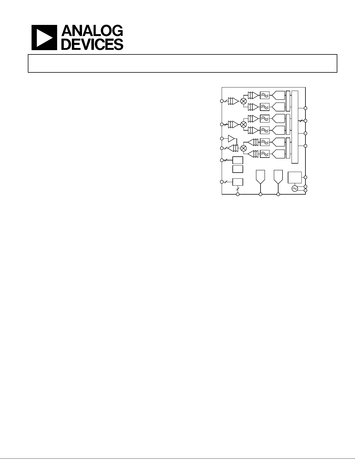
FUNCTIONAL BLOCK DIAGRAM
AD9354
RX1_N, RX1_P
RX2_N, RX2_P
PW_DET
TX_N, TX_P
SWITCHING*
(GPO0 TO GPO3)
SPI PORT
*RADIO SWI T CHI NG IS ONE POS SIBLE USE FO R THE GPO PI NS .
2
2
2
4
RADIO
GPO
LDOs
4
CTRL
2
CTRL_OUT[1:0] AUXADC AUXDAC
Figure 1.
channel filters produce a 10-bit output signal at the appropriate
sample rate determined by the bandwidth mode. The transmit
path interpolates 10-bit input data before converting it to the
analog domain, and then upconverting it to the carrier frequency.
The highly linear transmit path has excellent spectral purity
with sideband noise less than −134 dBm/Hz at 22 MHz offset,
and it offers an error vector magnitude (EVM) of −38 dB at
0 dBm output power. The transmit power is detected by an
accurate power detector with a range of more than 40 dB and
0.5 dB steps. The output power can be calibrated at the factory
by a single measurement.
The reference frequency is produced by an internal digitally
controlled crystal oscillator (DCXO) that has a programmable
frequency offset correction with a resolution of 0.012 ppm, thus
reducing the total bill of materials (BOM) of the device.
An internal auxiliary ADC and an auxiliary digital-to-analog
converter (DAC) are available for system monitoring and
control. Four general-purpose I/Os are also included and can be
register programmed or automatically sequenced by a userdefined state machine. Mode control is via a 3- or 4-wire serial
port and four real-time I/O control pins. The AD9354 is
powered either from a single 3.3 V supply or, for power savings,
from dual supplies and contains on-chip low dropout (LDO)
regulators. The AD9354 is packaged in an 8 mm × 8 mm, 56-lead
lead frame chip scale package (LFCSP).
One Technology Way, P.O. Box 9106, Norwood, MA 02062-9106, U.S.A.
Tel: 781.329.4700 www.analog.com
Fax: 781.461.3113 ©2008 Analog Devices, Inc. All rights reserved.
ADC
ADC
ADC
ADC
ADC
DAC
DAC
DAC
FILTER FILTER FILTER
LO
SYNTH
10
DATA INTERF ACE
TXNRX
D[9:0]
DATA_CLK
DV/FB_CLK
REFCLK
XTALP
XTALN
07602-001
Page 2

AD9354
NOTES
©2008 Analog Devices, Inc. All rights reserved. Trademarks and
registered trademarks are the property of their respective owners.
D07602F-0-7/08(Sp0)
Rev. Sp0 | Page 2 of 2
 Loading...