

Page 1
4 × 1 Wideband
a
FEATURES
34 MHz Full Power Bandwidth
60.1 dB Gain Flatness to 8 MHz
72 dB Crosstalk Rejection @ 10 MHz
0.038/0.01% Differential Phase/Gain
Cascadable for Switch Matrices
MIL-STD-883 Compliant Versions Available
APPLICATIONS
Video Routing
Medical Imaging
Electro Optics
ECM Systems
Radar Systems
Data Acquisition
GENERAL DESCRIPTION
The AD9300 is a monolithic high speed video signal multiplexer
usable in a wide variety of applications.
Its four channels of video input signals can be randomly
switched at megahertz rates to the single output. In addition,
multiple devices can be configured in either parallel or cascade
arrangements to form switch matrices. This flexibility in using
the AD9300 is possible because the output of the device is in a
high-impedance state when the chip is not enabled; when the
chip is enabled, the unit acts as a buffer with a high input impedance and low output impedance.
An advanced bipolar process provides fast, wideband switching
capabilities while maintaining crosstalk rejection of 72 dB at
10 MHz. Full power bandwidth is a minimum 27 MHz. The
device can be operated from ±10 V to ±15 V power supplies.
Video Multiplexer
AD9300
FUNCTIONAL BLOCK DIAGRAM
(Based on Cerdip)
The AD9300K is available in a 16-pin ceramic DIP and a
20-pin PLCC and is designed to operate over the commercial
temperature range of 0°C to +70°C. The AD9300TQ is a
hermetic 16-pin ceramic DIP for military temperature range
(–55°C to +125°C) applications. This part is also available processed to MIL-STD-883. The AD9300 is available in a 20-pin
LCC as the model AD9300TE, which operates over a temperature range of –55°C to +125°C.
The AD9300 Video Multiplexer is available in versions compliant with MIL-STD-883. Refer to the Analog Devices Military
Products Databook or current AD9300/883B data sheet for detailed specifications.
PIN DESIGNATIONS
DIP
REV. A
Information furnished by Analog Devices is believed to be accurate and
reliable. However, no responsibility is assumed by Analog Devices for its
use, nor for any infringements of patents or other rights of third parties
which may result from its use. No license is granted by implication or
otherwise under any patent or patent rights of Analog Devices.
LCC and PLCC
One Technology Way, P.O. Box 9106, Norwood, MA 02062-9106, U.S.A.
Tel: 617/329-4700 World Wide Web Site: http://www.analog.com
Fax: 617/326-8703 © Analog Devices, Inc., 1996
Page 2

AD9300–SPECIFICA TIONS
ELECTRICAL CHARACTERISTICS
(6VS = 612 V 6 5%; CL = 10 pF; RL = 2 kV, unless otherwise noted)
COMMERCIAL
08C to +708C
Test AD9300KQ/KP
Parameter (Conditions) Temp Level Min Typ Max Units
INPUT CHARACTERISTICS
Input Offset Voltage +25°CI 3 10 mV
Input Offset Voltage Full VI 14 mV
Input Offset Voltage Drift
2
Full V 75 µV/°C
Input Bias Current +25°C I 15 37 µA
Input Bias Current Full VI 55 µA
Input Resistance +25°C V 3.0 MΩ
Input Capacitance +25°CV 2 pF
Input Noise Voltage (dc to 8 MHz) +25°CV 16 µV rms
TRANSFER CHARACTERISTICS
Voltage Gain
Voltage Gain
DC Linearity
Gain Tolerance (V
3
3
4
= ±1 V)
IN
+25°C I 0.990 0.994 V/V
Full VI 0.985 V/V
+25°C V 0.01 %
dc to 5 MHz +25°C I 0.05 0.1 dB
5 MHz to 8 MHz +25°C I 0.1 0.3 dB
Small-Signal Bandwidth +25°C V 350 MHz
(V
= 100 mV p-p)
IN
Full Power Bandwidth
(V
= 2 V p-p)
IN
5
+25°C I 27 34 MHz
Output Swing Full VI ±2V
Output Current (Sinking @ = +25°C) +25°CV 5 mA
Output Resistance +25°C IV, V 9 15 Ω
DYNAMIC CHARACTERISTICS
Slew Rate
6
+25°C I 170 215 V/µs
Settling Time (to 0.1% on ±2 V Output) +25°C IV 70 100 ns
Overshoot
To T-Step
To Pulse
Differential Phase
Differential Gain
Crosstalk Rejection
Three Channels
One Channel
SWITCHING CHARACTERISTICS
AX Input to Channel HIGH Time
A
Input to Channel LOW Time14 (t
X
Enable to Channel ON Time
Enable to Channel OFF Time
Switching Transient
7
8
9
9
10
11
12
13
(t
HIGH
) +25°C I 35 45 ns
LOW
15
(tON) +25°C I 35 45 ns
16
(t
) +25°C I 35 45 ns
17
OFF
+25°C V <0.1 %
+25°C V <10 %
+25°C IV 0.03 0.1 °
+25°C IV 0.01 0.1 %
+25°CIV 68 72 dB
+25°CIV 70 76 dB
) +25°C I 40 50 ns
+25°CV 60 mV
DIGITAL INPUTS
Logic “1” Voltage Full VI 2 V
Logic “0” Voltage Full VI 0.8 V
Logic “1” Current Full VI 5 µA
Logic “0” Current Full VI 1 µA
POWER SUPPLY
Positive Supply Current (+12 V) +25°C I 13 16 mA
Positive Supply Current (+12 V) Full VI 13 16 mA
Negative Supply Current (–12 V) +25°C I 12.5 15 mA
Negative Supply Current (–12 V) Full VI 12.5 16 mA
Power Supply Rejection Ratio Full VI 67 75 dB
(±V
= ±12 V ± 5%)
S
Power Dissipation (±12 V)
l8
+25°C V 306 mW
–2–
REV. A
Page 3

AD9300
NOTES
11
Permanent damage may occur if any one absolute maximum rating is exceeded. Functional operation is not implied, and device reliability may be impaired by
exposure to higher-than-recommended voltages for extended periods of time.
12
Measured at extremes of temperature range.
13
Measured as slope of V
14
Measured as worst deviation from endpoint fit with VIN = ±1 V.
15
Full Power Bandwidth (FPBW) based on Slew Rate (SR). FPBW = SR/2 π V
16
Measured between 20% and 80% transition points of ±1 V output.
17
T-Step = Sin2 × Step, when Step between 0 V and +700 mV points has 10% to 90% risetime = 125 ns.
18
Measured with a pulse input having slew rate >250 V/µs.
19
Measured at output between 0.28 V dc and 1.0 V dc with VIN = 284 mV p-p at 3.58 MHz and 4.43 MHz.
10
This specification is critically dependent on circuit layout. Value shown is measured with selected channel grounded and 10 MHz 2 V p-p signal applied to remaining
three channels. If selected channel is grounded through 75 Ω, value is approximately 6 dB higher.
11
This specification is critically dependent on circuit layout. Value shown is measured with selected channel grounded and 10 MHz 2 V p-p signal applied to one other
channel. If selected channel is grounded through 75 Ω, value is approximately 6 dB higher. Minimum specification in ( ) applies to DIPs.
12
Consult system timing diagram.
13
Measured from address change to 90% point of –2 V to +2 V output LOW-to-HIGH transition.
14
Measured from address change to 90% point of +2 V to –2 V output HIGH-to-LOW transition.
15
Measured from 50% transition point of ENABLE input to 90% transition of 0 V to –2 V and 0 V to +2 V output.
16
Measured from 50% transition point of ENABLE input to 10% transition of +2 V to 0 V and –2 V to 0 V output.
17
Measured while switching between two grounded channels.
18
Maximum power dissipation is a package-dependent parameter related to the following typical thermal impedances:
16-Pin Ceramic θJA = 87°C/W; θJC = 25°C/W
20-Pin LCC θJA = 74°C/W; θJC = 10°C/W
20-Pin PLCC θJA = 71°C/W; θ
Specifications subject to change without notice.
versus VIN with VIN = ±1 V.
OUT
= 26°C/W
JC
PEAK
ABSOLUTE MAXIMUM RATINGS
l
Supply Voltages (±VS) . . . . . . . . . . . . . . . . . . . . . . . . . . ±16 V
Analog Input Voltage Each Input
(IN
thru IN4) . . . . . . . . . . . . . . . . . . . . . . . . . . . . . ±3.5 V
1
Differential Voltage Between Any Two
Inputs (IN
Digital Input Voltages (A
thru IN4) . . . . . . . . . . . . . . . . . . . . . . . . . . . 5 V
1
, A1, ENABLE) . . .–0.5 V to +5.5 V
0
Output Current
Sinking . . . . . . . . . . . . . . . . . . . . . . . . . . . . . . . . . . . 6.0 mA
Sourcing . . . . . . . . . . . . . . . . . . . . . . . . . . . . . . . . . . 6.0 mA
Operating Temperature Range
AD9300KQ/KP . . . . . . . . . . . . . . . . . . . . . . . 0°C to +70°C
Storage Temperature Range . . . . . . . . . . . . –65°C to +150°C
Junction Temperature . . . . . . . . . . . . . . . . . . . . . . . . +175°C
Lead Soldering (10 sec) . . . . . . . . . . . . . . . . . . . . . . . +300°C
ORDERlNG GUlDE
Temperature Package
Device Range Description Option
AD9300KQ 0°C to +70°C 16-Pin Cerdip, Commercial Q-16
AD9300TE/883B
AD9300TQ/883B
AD9300KP 0°C to +70°C 20-Pin PLCC, Commercial P-20A
NOTES
1
E = Ceramic Leadless Chip Carrier; P = Plastic Leaded Chip Carrier; Q = Cerdip.
2
For specifications, refer to Analog Devices Military Products Databook .
2
–55°C to +125°C 20-Pin LCC, Military Temperature E-20A
2
–55°C to +125°C 16-Pin Cerdip, Military Temperature Q-16
EXPLANATION OF TEST LEVELS
Test Level I – 100% production tested.
Test Level II – 100% production tested at +25°C, and
sample tested at specified temperatures.
Test Level III – Sample tested only.
Test Level IV – Parameter is guaranteed by design and
characterization testing.
Test Level V – Parameter is a typical value only.
Test Level VI – All devices are 100% production tested at
+25°C. 100% production tested at tempera-
ture extremes for military temperature de-
vices; sample tested at temperature extremes
for commercial/industrial devices.
1
CAUTION
ESD (electrostatic discharge) sensitive device. Electrostatic charges as high as 4000 V readily
accumulate on the human body and test equipment and can discharge without detection.
Although the AD9300 features proprietary ESD protection circuitry, permanent damage may
occur on devices subjected to high energy electrostatic discharges. Therefore, proper ESD
precautions are recommended to avoid performance degradation or loss of functionality.
REV. A
–3–
WARNING!
ESD SENSITIVE DEVICE
Page 4

AD9300
AD9300 BURN-IN DIAGRAM
FUNCTIONAL DESCRIPTION
IN
–IN
1
4
Four analog input channels.
GROUND Analog input shielding grounds, not internally con-
nected. Connect each to external low-impedance
ground as close to device as possible.
A
0
One of two TTL decode control lines required for
channel selection. See Logic Truth Table.
A
1
One of two TTL decode control lines required for
channel selection. See Logic Truth Table.
ENABLE TTL-compatible chip enable. In enabled mode
(logic HIGH), output signal tracks selected input
channel; in disabled mode (logic LOW), output is
high impedance and no signal appears at output.
–V
S
Negative supply voltage; normally –10 V dc to
–15 V dc.
+V
S
Positive supply voltage; normally +10 V dc to
+15 V dc.
OUTPUT Analog output. Tracks selected input channel when
enabled.
BYPASS Bypass terminal for internal bias line; must be
decoupled externally to ground through 0.1 µF
capacitor.
GROUND Analog signal and power supply ground return.
RETURN
SUGGESTED LAYOUT OF AD9300
PC BOARD
METALIZATION PHOTOGRAPH
MECHANICAL INFORMATION
Die Dimensions . . . . . . . . . . . . . . . . .84 × 104 × 18 (max) mils
Pad Dimensions . . . . . . . . . . . . . . . . . . . . . . . .4 × 4 (min) mils
Metalization . . . . . . . . . . . . . . . . . . . . . . . . . . . . . . . Aluminum
Backing . . . . . . . . . . . . . . . . . . . . . . . . . . . . . . . . . . . . . . None
Substrate Potential . . . . . . . . . . . . . . . . . . . . . . . . . . . . . . . –V
Passivation . . . . . . . . . . . . . . . . . . . . . . . . . . . . . . . . Oxynitride
Die Attach . . . . . . . . . . . . . . . . . . . . . . . . . . . . . Gold Eutectic
Bond Wire . . . . . . . . 1.25 mil, Aluminum; Ultrasonic Bonding
or 1 mil, Gold; Gold Ball Bonding
S
AD9300 Timing Diagram
–4–
LOGIC TRUTH TABLE
ENABLE A1A0OUTPUT
0 X X High Z
100IN
101IN
110IN
111IN
1
2
3
4
REV. A
Page 5

AD9300
THEORY OF OPERATION
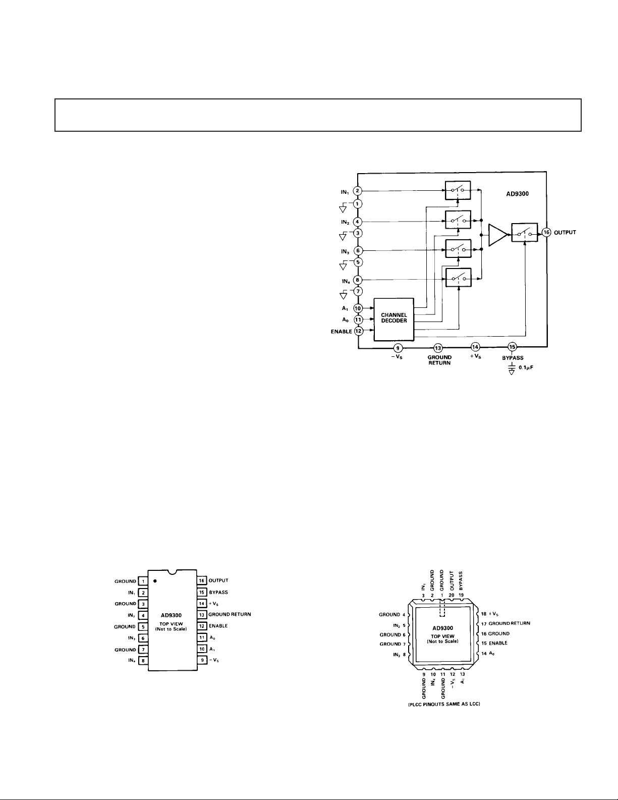
Refer to the functional block diagram of the AD9300.
As shown in the drawing, this diagram is based on the pinouts of
the DIP packaging of the models AD9300KQ and AD9300TQ.
The AD9300KP and AD9300TE are packaged in 20-pin surface
mount packages. The extra pins are used for ground connections;
the theory of operation remains the same.
The AD9300 Video Multiplexer allows the user to connect any
one of four analog input channels (IN
device and to switch between channels at megahertz rates.
The input channel, which is connected to the output is determined by a 2-bit TTL digital code applied to A
lected input will not appear at the output unless a digital “1” is
also applied to the ENABLE input pin; unless the output is
enabled, it is a high impedance. Necessary combinations to accomplish channel selection are shown in the Logic Truth Table.
Figure 1. Input and Output Equivalent Circuits
–IN4) to the output of the
1
and A1. The se-
0
Bipolar construction used in the AD9300 ensures that the input
impedance of the device remains high and will not vary with
power supply voltages. This characteristic makes the AD9300,
in effect, a switchable-input buffer. An onboard bias network
makes the performance of the AD9300 independent of applied
supply voltages, which can have any nominal value from
±10 V dc to ±15 V dc.
Although the primary application for the AD9300 is the routing
of video signals, the harmonic and dynamic attributes of the
device make it appropriate for other applications. The AD9300
has exceptional performance when switching video signals and
can also be used for switching other analog signals requiring
greater dynamic range and/or precision than those in video.
As shown in Figure 1, each analog input is connected to the
base of a bipolar transistor. If Channel 1 is selected, a current
switch is closed and routes current through the input transistor
for Channel 1.
If Channel 2 is then selected by the digital inputs, the current
switch for Channel 1 is opened and the current switch for Channel 2 is closed. This causes current to be routed away from the
Channel 1 transistor and into the Channel 2 input transistor.
Whenever a channel’s input device is carrying current, the analog input applied to that channel is passed to the output stage.
The operation of the output stage is similar to that of the input
stages. Whenever the output stage is enabled with a HIGH digital “1” signal at the ENABLE pin, the output transistor will
carry current and pass the selected analog input.
When the output stage is disabled (by virtue of the ENABLE
pin being driven LOW with a digital “0”), the output current
switch is opened. This routes the current to other circuits within
the AD9300 that keep the output transistor biased “off.” These
circuits require approximately 1 µA of bias current from the load
connected to the output of the multiplexer. In the absence of a
terminating load and the resulting dc bias, the output of the
AD9300 “floats” at –2.5 V.
In summary, when the AD9300 is enabled by the ENABLE pin
being driven HIGH with a digital “1,” the selected analog input
channel acts as a buffer for the input and the output of the multiplexer is a low impedance. When the AD9300 is disabled with
a digital “0” LOW signal, the selected channel acts as an open
switch for the input, and the output of the unit becomes a high
impedance. This characteristic allows the user to wire-or several
AD9300 Analog Multiplexers together to form switch matrices.
REV. A
–5–
Page 6

AD9300
AD9300 APPLICATIONS
To ensure optimum performance from circuits using the AD9300,
it is important to follow a few basic rules that apply to all high
speed devices.
A large, low-impedance ground plane under the AD9300 is
critical. Generally, GROUND and GROUND RETURN connections should be connected solidly to this plane. GROUND
pin connections are signal isolation grounds that are not
Figure 2. 4 x 1 AD9300 Multiplexer with Buffered Output
Driving 75
Ω
Coaxial Cable
connected internally; they can be left unconnected, but there
may be some degradation in crosstalk rejection. GROUND RETURN, on the other hand, serves as the internal ground reference for the AD9300 and, without exception, should be
connected to the ground plane.
The output stage of the unit is capable of driving a 2 kΩi10 pF
load. Larger capacitive loads may limit full power bandwidth
and increase t
(the interval between the 50% point of the
OFF
ENABLE high-to-low transition and the instant the output
becomes a high impedance).
For applications such as driving cables (see Figure 2), output
buffers are recommended.
It is recommended that the AD9300 be soldered directly into
circuit boards rather than using socket assemblies. If sockets
must be used, individual pin sockets are preferred rather than a
socket assembly. A second requirement for proper high speed
design involves decoupling the power supply and
internal bias supply lines from ground to improve noise immunity. Chip capacitors are recommended for connecting 0.1 µF
and 0.01 µF capacitors between ground and the ± V
supplies
S
(Pins 9 and 14) and the BYPASS connection (Pin 15).
Figure 3. Harmonic Distortion vs.
Frequency
Figure 6. Test Circuit for Harmonic Distortion, Pulse
Response, T-Step Response and Disable Characteristics
Figure 4. Output vs. Frequency
–6–
Figure 5. Crosstalk vs. Frequency
Figure 7. Crosstalk Rejection Test Circuit
REV. A
Page 7

AD9300
Figure 8. Pulse Response
Figure 9. T-Step Response
CROSSPOINT CIRCUIT APPLICATIONS
Four AD9300 multiplexers can be used to implement an 8 × 2
crosspoint, as shown in Figure 11. The circuit is modular in
concept, with each pair of multiplexers (#1 and #2; #3 and #4)
forming an 8 × 1 crosspoint. When the inputs to all four units
are connected as shown, the result is an 8 × 2 crosspoint circuit.
Figure 10. Enable to Channel
“Off” Response
The truth table describes the relationships among the digital inputs (D
input is selected at the outputs (OUT
) and the analog inputs (S1-S8) and which signal
0–D5
and OUT2). The num-
1
ber of crosspoint modules that can be connected in parallel is
limited by the drive capabilities of the input signal sources. High
input impedance (3 MΩ) and low input capacitance (2 pF) of
the AD9300 help minimize this limitation.
8 3 2 Crosspoint Truth Table
D
2
D
1
D
0
OUT
1
or or or or
D
5
00 0S
00 1S
01 0S
01 1S
10 0S
10 1S
11 0S
11 1S
D
4
D
3
OUT
2
1
2
3
4
5
6
7
8
Adding to the number of inputs applied to each crosspoint
module is simply a matter of adding AD9300 multiplexers in
parallel to the module. Eight devices connected in parallel result
in a 32 × 1 crosspoint, which can be used with input signals having 30 MHz bandwidth and 1 V peak-to-peak amplitude. Even
more AD9300 units can be added if input signal amplitude
and/or bandwidth are reduced; if they are not, distortion of the
output signals can result.
When an AD9300 is enabled, its low output impedance causes
the “off” isolation of disabled parallel devices to be greater than
the crosstalk rejection of a single unit.
Figure 11. 8 x 2 Signal Crosspoint Using Four AD9300
Multiplexers
REV. A
–7–
Page 8

AD9300
OUTLINE DIMENSIONS
Dimensions shown in inches and (mm).
16-Pin Cerdip (Q) Package
20-Pin LCC (E) Package
C1184a–21–11/90
20-Pin PLCC (P) Package
–8–
PRINTED IN U.S.A.
REV. A
 Loading...