

Page 1
8-Bit, 500 MSPS, 1.8 V
A
A
FEATURES
Single 1.8 V supply operation
SNR: 49.3 dBFS at 200 MHz input at 500 MSPS
SFDR: 65 dBc at 200 MHz input at 500 MSPS
Low power: 315 mW at 500 MSPS
On-chip interleaved clocking
On-chip reference and track-and-hold
1.2 V p-p analog input range for each channel
Differential input with 500 MHz bandwidth
LVDS-compliant digital output
On-chip voltage reference and sample-and-hold circuit
DNL: ±0.2 LSB
Serial port control options
Interleaved clock timing adjustment
Offset binary, Gray code, or twos complement data format
Optional clock duty cycle stabilizer
Built-in selectable digital test pattern generation
Pin-programmable power-down function
Available in 48-lead LFCSP
APPLICATIONS
Battery-powered instruments
Handheld scope meters
Low cost digital oscilloscopes
OTS: video over fiber
Analog-to-Digital Converter (ADC)
AD9286
GENERAL DESCRIPTION
The AD9286 is an 8-bit, monolithic sampling, analog-to-digital
converter (ADC) that supports interleaved operation and is
optimized for low cost, low power, and ease of use. Each ADC
operates at up to a 250 MSPS conversion rate with outstanding
dynamic performance.
The AD9286 takes a single sample clock and, with an on-chip
clock divider, time interleaves the two ADC cores (each running
at one-half the clock frequency) to achieve the rated 500 MSPS.
By using the SPI, the user can accurately adjust the timing of the
sampling edge per ADC to minimize the image spur energy.
The ADC requires a single 1.8 V supply and an encode clock for
full performance operation. No external reference components
are required for many applications. The digital outputs are LVDS
compatible.
The AD9286 is available in a Pb-free, 48-lead LFCSP that is
specified over the industrial temperature range of −40°C to +85°C.
PRODUCT HIGHLIGHTS
1. Integrated 8-Bit, 500 MSPS ADC.
2. Single 1.8 V Supply Operation with LVDS Outputs.
3. Power-Down Option Controlled via a Pin-Programmable
Setting.
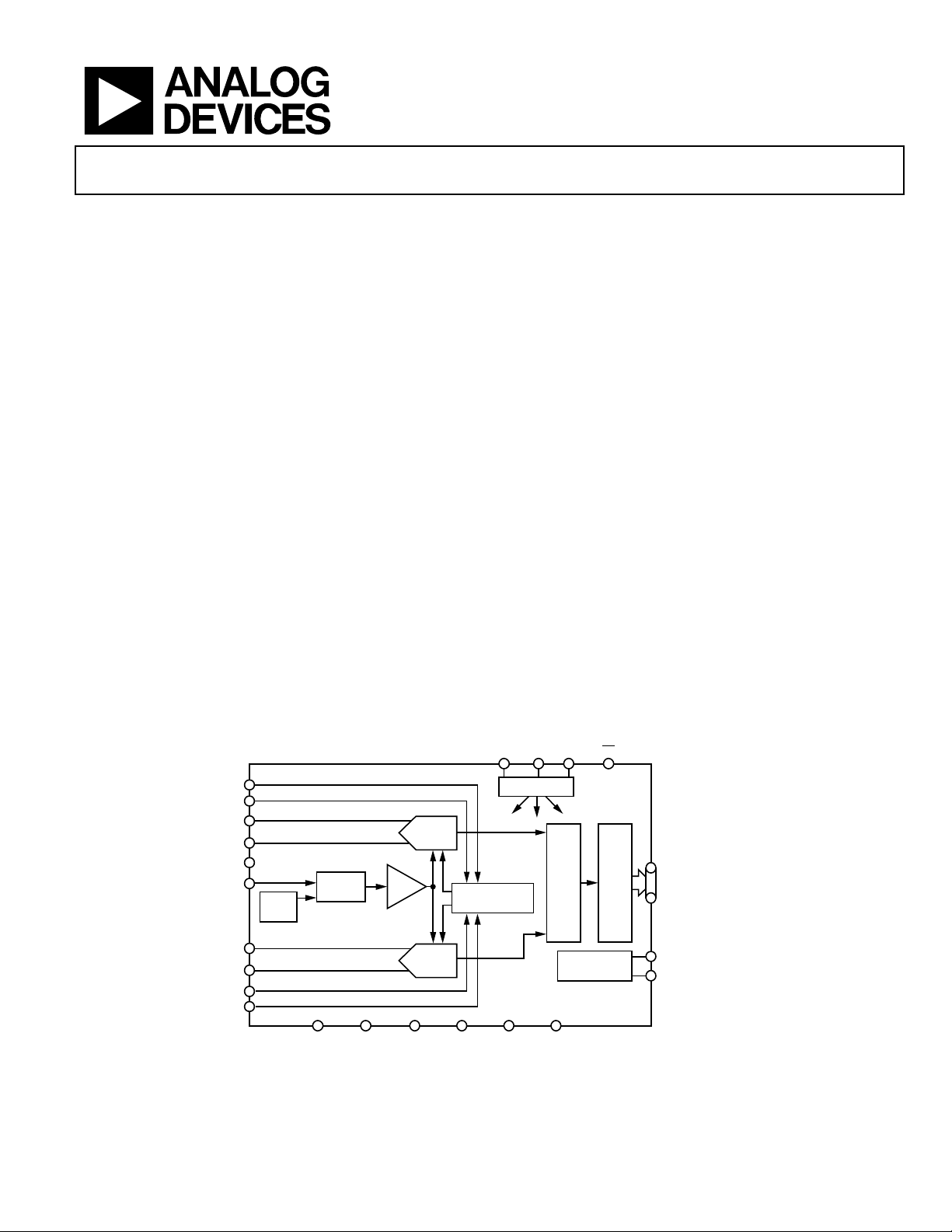
FUNCTIONAL BLOCK DIAGRAM
CLK+
CLK–
VIN1+
VIN1–
VCM
VREF
1.0V
V
REF
VIN2–
VIN2+
UXCLK–
UXCLK+
Rev. A
Information furnished by Analog Devices is believed to be accurate and reliable. However, no
responsibility is assumed by Analog Devices for its use, nor for any infringements of patents or other
rights of third parties that may result from its use. Specifications subject to change without notice. No
license is granted by implication or otherwise under any patent or patent rights of Analog Devices.
Trademarks and registered trademarks are the property of their respective owners.
REF
SELECT
RBIAS AUXCLKEN AGND AVDD DRVDD DRGND
ADC
×1.5
ADC
SDIO/
PWDN
CLOCK
MANAGEMENT
Figure 1.
One Technology Way, P.O. Box 9106, Norwood, MA 02062-9106, U.S.A.
Tel: 781.329.4700 www.analog.com
Fax: 781.461.3113 ©2011 Analog Devices, Inc. All rights reserved.
CSB
SPI
SCLK
OE
OUTPUT
INTERLEAVE
DCO
GENERATION
AD9286
D7+ (MSB), D7– (MSB)
LVDS
D0+ (LSB), D0– (LSB)
OUTPUT BUFFER
DCO+
DCO–
09338-001
 Loading...