

Page 1
Sigma-Delta (CTSD) Analog-to-Digital Converters
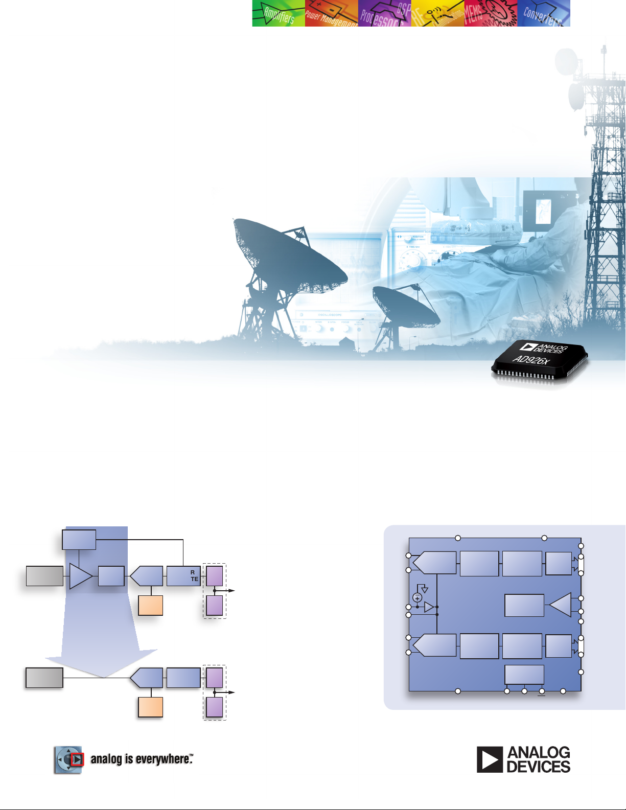
ANALOG
FRONT END
GAIN
CONTROL
POWER
ESTIMATE
AMP LPF
ANTIALIAS
FILTER
ADC
CLOCK
NETWORK INTERFACE NETWORK INTERFACE
DSP
DSP
REDUCE PART COUNT
REDUCE SYSTEM COST
REDUCE DESIGN TIME
ANALOG
FRONT END
POWER
ESTIMATE
ADC
CLOCK
DSP
DSP
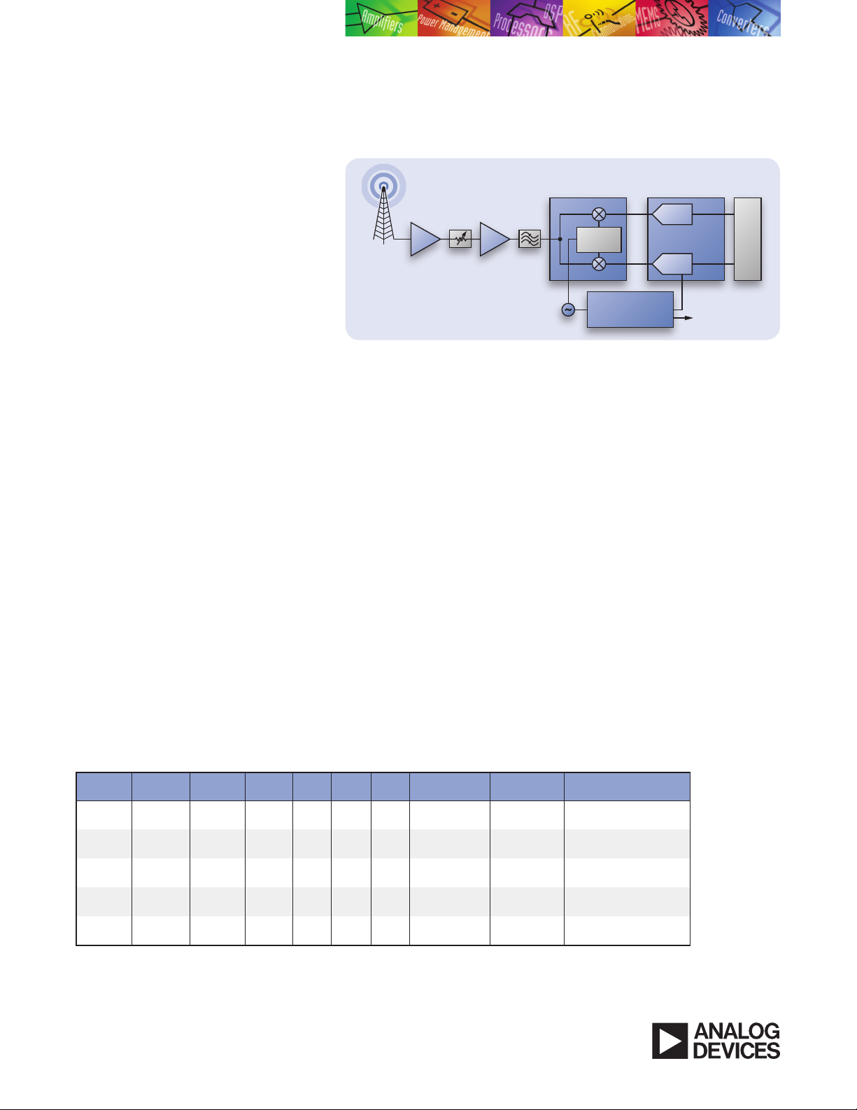
CT «-
MODULATOR
LOW-PASS
DECIMATION
FILTER
VIN+A
VIN–A
VIN+B
VIN–B
VREF
AGND SDIO SCLK
SAMPLE
RATE
CONVERTER
PHASE-
LOCKED
LOOP
CMOS
BUFFER
CT «-
MODULATOR
LOW-PASS
DECIMATION
FILTER
SAMPLE
RATE
CONVERTER
CMOS
BUFFER
DGND
AVDD
AD9262
DRVDD
D15A
ORA
D0A
D15B
D0B
CLK+
CLK–
DCO
ORB
CFILT
SERIAL
INTERFACE
CS
Features
Excellent low noise, wide bandwidth,
and high level of integration
SNR: 84.5 dBFS to 10 MHz input•
SFDR: 87 dBc to 10 MHz input•
Noise figure: 15 dB•
Input impedance of 1 k• Ω
Power: 350 mW/channel•
1.8 V analog supply•
1.8 V to 3.3 V output supply•
Output data rate: 30 MSPS to 160 MSPS •
Selectable bandwidth•
5 MHz/10 MHz/20 MHz complex•
2.5 MHz/5 MHz/10 MHz dual real•
Integrated decimation filter•
Integrated sample rate converter•
Integrated PLL clock multiplier•
Low drift voltage reference•
Benefits
Simplifies system design
No antialias filters required•
Removes need for driver amplifier•
Simplifies or eliminates need for AGC•
Relaxes system linearity requirements•
Capable of high input voltage swings •
AD926x Family
16-Bit, 10 MHz Bandwidth, Continuous-Time
New Family of CTSD ADCs Efficiently Achieves High Dynamic Range
and Wide Bandwidth Performance
Data converters play a pivotal role in a tremendously wide and growing range of electronic
systems such as wireless communications, medical imaging, and instrumentation. The
rapidly escalating performance requirements of today’s end applications are demanding
ever-increasing sampling speeds in combination with higher resolution, superior noise
performance, and lower power consumption. Engineers typically have had to settle for a
compromise between these challenging requirements.
With the advent of continuous-time Σ-∆ analog-to-digital converters, designers can
achieve breakthrough performance in their designs without compromising on bandwidth,
noise performance, power
consumption, and ease of use.
Utilizing an innovative converter
architecture, the AD926x family of
CTSD ADCs from Analog Devices
offers up to 10 MHz of bandwidth
with 86 dB dynamic range at only
350 mW/channel. This combination
of performance characteristics
enables designers to build next
generation system architectures
with fewer components, running
on less power, in smaller form
factors, and with less design and
test time than before.
AD9262 Block Diagram.
www.analog.com/AD9262
Page 2
ADC
ADC
90˚ PHASE
SHIFTER
AD9262
16-BIT CTSD ADC
ADL5382
IQ DEMODULATOR
FPGA DIGITAL
PROCESSING
AD9520
CLOCK GENERATION
AND DISTRIBUTION
TO Tx/FPGA
AMPLNA
MAIN Rx
CTSD ADC System Level Benefits
The AD926x family of CTSD ADCs offers significant
system level advantages to the design engineer
by providing a high level of dynamic performance,
efficiency, integration, and ease of use.
Performance
The ADC provides an extremely low 15 dB noise figure,
which is nearly a 7 dB improvement over current state
of the art wideband converters. The low noise figure
reduces the front end gain, thereby relaxing linearity
requirements in an RF system. In addition, the high
dynamic range of 86 dB makes it possible to eliminate
the automatic gain control commonly employed in many communication systems. Furthermore, the purely resistive 1 kΩ input
structure of the converter significantly relaxes the requirements of the ADC driver amplifier. This results in the AD926x requiring
–3 dBm input power to achieve a 2 V p-p input voltage swing, which is 7 dBm lower than conventional switched capacitor input
converters. In fact, if no additional gain is required in the system, the driver can be completely eliminated.
Efficiency
At approximately 350 mW/channel the AD926x is at least 2× lower in power consumption than converters with similar
dynamic range, noise performance, and bandwidths. In addition, the high dynamic range and ease of input drive help
reduce or eliminate signal chain components, providing further reductions in system level power consumption. The internal
low pass loop filter response attenuates aliases and out of band signals, thereby eliminating the need for an antialiasing
filter at the input of the ADC and resulting in a reduction of system level components.
Integration
In addition to their excellent performance and efficiency, the AD9262 and AD9261 have an integrated digital decimation
filter, sample rate converter, PLL clock multiplier, and voltage reference. The AD9267 is a 4-bit 640 MSPS modulator-only
version intended for offloading signal processing functions to FPGAs and other processors.
These unique features enabled by the CTSD architecture allow designers to significantly reduce or completely eliminate
the need for antialiasing filters, driver amplifiers, and automatic gain control used in conventional designs—thus reducing
cost, size, power consumption, and time to market for their products. An example of this is shown above using the AD9262
in combination with ADI’s high performance ADL5382 quadrature demodulator and AD9520 clock generation and distribution
products to implement a high performance and low part count 700 MHz to 2.7 GHz direct conversion receiver.
The AD926x family is available in several different versions including channel count, bandwidth, and level of integration.
AD926x Continuous-Time 𝚺-𝚫 Converter Family
Part
Number
AD9262 16 2.5 2 90.5 87 580
AD9262-5 16 5 2 87.5 87 630
AD9262-10 16 10 2 84.5 87 675
AD9267
AD9261-10 16 10 1 84.5 87 350
* AD9267 is a CTSD modulator providing 4-bit, 640 MSPS LVDS output enabling 85 dBFS SNR over a dc to 10 MHz BW.
©2008 Analog Devices, Inc. All rights reserved.
Trademarks and registered trademarks are the property
of their respective owners.
Printed in the U.S.A. PH07863-.15-11/08 www.analog.com/AD9262
Resolution
modulator*
(Bits)
4-bit
Bandwidth
(MHz)
10*
Channel
Count
2
SNR
(dBFS)
Example Application: Communication Receiver.
SFDR
Power
(dBFS)
87 400 4-bit LVDS
85*
Output Interface Package Integration
(mW)
16-bit CMOS
16-bit CMOS
16-bit CMOS
16-bit CMOS
9 mm × 9 mm
64-lead LFCSP
9 mm × 9 mm
64-lead LFCSP
9 mm × 9 mm
64-lead LFCSP
9 mm × 9 mm
64-lead LFCSP
7 mm × 7 mm
48-lead LFCSP
PLL, decimation filters,
sample rate converter
PLL, decimation filters,
sample rate converter
PLL, decimation filters,
sample rate converter
PLL
PLL, decimation filters,
sample rate converter
Analog Devices, Inc.
Worldwide Headquarters
Analog Devices, Inc.
One Technology Way
P.O. Box 9106
Norwood, MA 02062-9106
U.S.A.
Tel: 781.329.4700
(800.262.5643,
U.S.A. only)
Fax: 781.461.3113
Analog Devices, Inc.
Europe Headquarters
Analog Devices, Inc.
Wilhelm-Wagenfeld-Str. 6
80807 Munich
Germany
Tel: 49.89.76903.0
Fax: 49.89.76903.157
Analog Devices, Inc.
Japan Headquarters
Analog Devices, KK
New Pier Takeshiba
South Tower Building
1-16-1 Kaigan, Minato-ku,
Tokyo, 105-6891
Japan
Tel: 813.5402.8200
Fax: 813.5402.1064
Analog Devices, Inc.
Southeast Asia
Headquarters
Analog Devices
22/F One Corporate Avenue
222 Hu Bin Road
Shanghai, 200021
China
Tel: 86.21.2320.8000
Fax: 86.21.2320.8222
 Loading...