Page 1

16-Bit, 10 MHz Bandwidth, 30 MSPS to
A
V
160 MSPS Continuous Time Sigma-Delta ADC
FEATURES
SNR: 83 dB (85 dBFS) to 10 MHz input
SFDR: 87 dBc to 10 MHz input
Noise figure: 15 dB
Input impedance: 1 kΩ
Power: 340 mW
1.8 V analog supply operation
1.8 V to 3.3 V output supply
Selectable bandwidth
2.5 MHz/5 MHz/10 MHz
Output data rate: 30 MSPS to 160 MSPS
Integrated decimation filters
Integrated sample rate converter
On-chip PLL clock multiplier
On-chip voltage reference
Offset binary, Gray code, or twos complement data format
Serial control interface (SPI)
APPLICATIONS
Data acquisition
Automated test equipment
Instrumentation
Medical imaging
VIN+
VIN–
VREF
CFILT
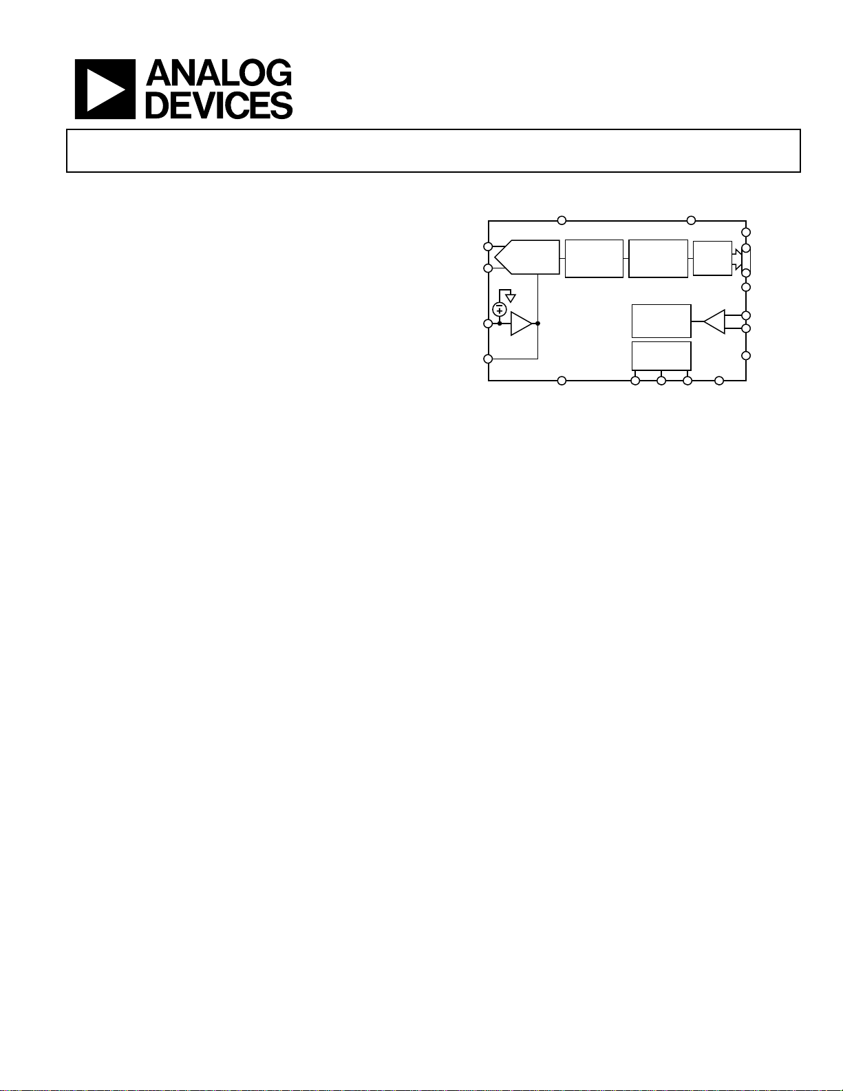
FUNCTIONAL BLOCK DIAGRAM
Σ-Δ
MODULATOR
DD
LOW-PASS
DECIMATION
FILTER
AD9261
AGND SDIO SCLK CSB
CONVERTER
Figure 1.
SAMPLE
RATE
PHASE
LOCKED
LOOP
SERIAL
INTERFACE
DRVDD
AD9261
OR
CMOS
BUFFER
DGND
D15
D0
PLL_
LOCKED
CLK+
CLK–
DCO
07803-001
GENERAL DESCRIPTION
The AD9261 is a single 16-bit analog-to-digital converter
(ADC) based on a continuous time (CT) sigma-delta (Σ-Δ)
architecture that achieves 87 dBc of dynamic range over a 10 MHz
input bandwidth. The integrated features and characteristics
unique to the continuous time Σ-Δ architecture significantly
simplify its use and minimize the need for external components.
The AD9261 has a resistive input impedance that relaxes the
requirements of the driver amplifier. In addition, a 32× oversampled fifth-order continuous time loop filter significantly attenuates
out-of-band signals and aliases, reducing the need for external
filters at the input.
An external clock input or the integrated integer-N PLL provides
the 640 MHz internal clock needed for the oversampled continuous time Σ-Δ modulator. On-chip decimation filters and sample
rate converters reduce the modulator data rate from 640 MSPS to a
user-defined output data rate from 30 MSPS to 160 MSPS,
enabling a more efficient and direct interface.
The digital output data is presented in offset binary, Gray code,
or twos complement format. A data clock output (DCO) is
provided to ensure proper timing with the receiving logic.
The AD9261 operates on a 1.8 V analog supply and a 1.8 V
to 3.3 V digital supply, consuming 340 mW. The AD9261 is
available in a 48-lead LFCSP and is specified over the industrial
temperature range (−40°C to +85°C).
PRODUCT HIGHLIGHTS
1. Continuous time Σ-Δ architecture efficiently achieves high
dynamic range and wide bandwidth.
2. Passive input structure reduces or eliminates the require-
ments for a driver amplifier.
3. An oversampling ratio of 32× and high order loop filter
provide excellent alias rejection reducing or eliminating the
need for antialiasing filters.
4. An integrated decimation filter, sample rate converter, PLL
clock multiplier, and voltage reference provide ease of use.
5. This part operates from a single 1.8 V analog power supply
and 1.8 V to 3.3 V output supply.
Rev. 0
Information furnished by Analog Devices is believed to be accurate and reliable. However, no
responsibility is assumed by Analog Devices for its use, nor for any infringements of patents or other
rights of third parties that may result from its use. Specifications subject to change without notice. No
license is granted by implication or otherwise under any patent or patent rights of Analog Devices.
Trademarks and registered trademarks are the property of their respective owners.
One Technology Way, P.O. Box 9106, Norwood, MA 02062-9106, U.S.A.
Tel: 781.329.4700 www.analog.com
Fax: 781.461.3113 ©2010 Analog Devices, Inc. All rights reserved.
 Loading...