

Page 1
PRELIMINAR Y TECHNICAL D A T A
a
14-Bit, 40/65 MSPS
Monolithic A/D Converter
Preliminary Technical Data
FEATURES
14-Bit, 65MSPS ADC
Low Power:
- 590mW at 65MSPS with Fin to Nyquist
- 340mW at 40MSPS with Fin to Nyquist
On-Chip Reference and Sample/Hold
750MHz Analog Input Bandwidth
SNR = 74dB up to Nyquist
SFDR = 83dB up to Nyquist
Differential Non Linearity Error = ±0.6LSB
Guaranteed No Missing Codes Over Full Temp range
1V to 2V p-p Differential Full Scale Analog Input Range
Single +5.0V Analog Supply, 3/5V Driver Supply
Out-of-Range Indicator
Straight Binary or Two’s Complement Output Data
48-Lead LQFP Package
APPLICATIONS
Communications Subsystems (Microcell, Picocell)
Medical and High End Imaging Equipment
Ultrasound Equipment
PRODUCT DESCRIPTION
The AD9244 is a monolithic, single 5V supply, 14-bit,
65MSPS Analog to Digital Converter with an on-chip,
high performance sample and hold amplifier and voltage
reference. The AD9244 uses a multi-stage differential
pipelined architecture with output error correction logic to
provide 14-bit accuracy at 65MSPS data rates and
guarantees no missing codes over the full operating
temperature range.
The AD9244 has an on-board, programmable voltage
reference. An external reference can also be chosen to suit
the DC accuracy and temperature drift requirements of the
application.
A differential clock input is used to control all internal
conversion cycles. The digital output data can be presented in straight binary or in two’s complement format.
An out of range (OTR) signal indicates an overflow condition, which can be used with the most significant bit to
determine low or high overflow.
Fabricated on an advanced CMOS process, the AD9244 is
available in a 48 pin surface mount plastic package (48
LQFP) and is specified for operation over the industrial
temperature range of (-40°C to +85°C).
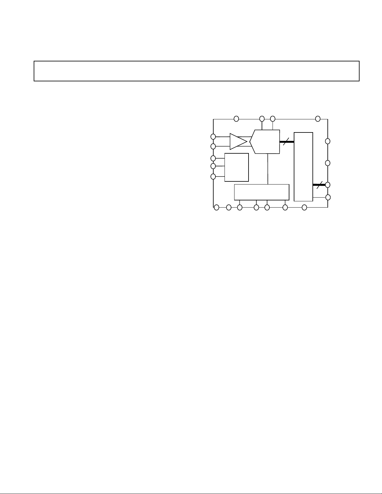
VIN+
VIN-
CLK+
CLK-
DUTY
AD9244
FUNCTIONAL BLOCK DIAGRAM
AVDD DRVDD
AD9244
SHA
TIMING
AGND DRGNDVREF REF
PRODUCT HIGHLIGHTS
Low Power—The AD9244 at 590mW consumes a fraction
of the power of presently available in existing, high speed
monolithic solutions.
On-Board Sample-and-Hold (SHA)—The versatile SHA
input can be configured for either single-ended or differential inputs.
Out of Range (OTR)—The OTR output bit indicates when
the input signal is beyond the AD9244’s input range.
Single Supply—The AD9244 uses a single +5V power supply simplifying system power supply design. It also features
a separate digital output driver supply line to accommodate
3V and 5V logic families.
IF Sampling—The AD9244 delivers outstanding performance at input frequencies beyond the first Nyquist zone.
Sampling at 65MSPS, with an input frequency of 100MHz,
the AD9244 delivers 70dB SNR and SFDR of 82dB.
REFT REFB
REFERENCE
VRCML
EIGHT
STAGE
PIPELINE
ADC
SENSE
14
REF
GND
OUTPUT REGISTER
DFS
OTR
DB13-DB0
14
OEB
REV. PrD 01/22/02
Information furnished by Analog Devices is believed to be accurate and
reliable. However, no responsibility is assumed by Analog Devices for its
use, nor for any infringements of patents or other rights of third parties
which may result from its use. No license is granted by implication or
otherwise under any patent or patent rights of Analog Devices.
One Technology Way, P.O. Box 9106, Norwood, MA 020629106, U.S.A.
Tel: 781/329-4700 www.analog.com
Fax: 781/326-8703 © Analog Devices, Inc., 2002
Page 2

PRELIMINARY TECHNICAL DAT A
AD9244–SPECIFICATIONS
DC SPECIFICATIONS
INPUTS, DIFFERENTIAL CLOCK INPUTS, EXTERNAL REFERENCE, T
(AVDD = +5 V , CLKVDD=3V , DRVDD = +3.0 V , f
to T
unless otherwise noted)
MIN
MAX
= 65 MSPS (-65) or 40MSPS (-40), INPUT RANGE = 2V p-p, DIFFERENTIAL ANALOG
SAMPLE
Test AD9244BST-65 AD9244BST-40
Parameter Temp Level Mi n T y p Ma x Min Typ Ma x Units
RESOLUTION Full VI 14 14 bits
DC ACCURACY
No Missing Codes Guaranteed Full VI 14 14 bits
Offset Error Full VI %FSR
Gain Error
Differential Nonlinearity (DNL)
Integral Nonlinearity (INL)
1
2
Full VI %FSR
2
Full IV L SB
+25°C I ±0.6 ±0.6 LS B
Full IV L SB
+25°C I ±1.9 ±1.3 LS B
TEMPERATURE DRIFT
Offset Error Full V ppm/°C
Gain Error
1
Full V ppm/°C
INTERNAL VOLTAGE REFERENCE
Output Voltage Error (2V VREF) Full VI ±3.9 ±3.9 mV
Load Regulation @ 1ma Full V
Output Voltage Error (1V VREF) Full V ±2.79 ±2.79 mV
Load Regulation @ 0.5ma Full V
INPUT REFERRED NOISE
VREF=2V +2 5°C V 0.82 0.79 LSB rms
VREF=1V +2 5°C V LSB rms
ANALOG INPUT
Input Voltage Range (differential)
VREF=2V +2 5°C V 2 2 V p-p
VREF=1V +2 5°C V 1 1 V p-p
Common Mode Voltage Full V 0.5 2 0.5 2 V
Input Capacitance
3
+25°CIV 7 7 pF
Input Bias Current +2 5°CIV 5 5 mA
Analog Bandwidth (full power) +2 5°C V 750 750 MHz
REFERENCE INPUT RESISTANCE Full V 5 5 kΩ
POWER SUPPLIES
Supply Voltages
AVDD Full IV 4.75 5.0 5.25 4.75 5.0 5.25 V
DRVDD Full IV 2.7 3.0 3.6 2.7 3.0 3.6 V
Supply Current
2
IAVDD
IDRVDD
2
Full IV 104 62 mA
+25°CI
Full IV 12 7.6 mA
+25°CI
POWER CONSUMPTION
DC Input
Sinewave Input
NOTES
1
Gain Error is based on the ADC only (with a fixed 1.0V external reference).
2
Measured at maximum clock rate, fIN = 2.4MHz, full scale sinewave, with approximately 5pF loading on each output bit.
3
Input capacitance refers to the effective capacitance between one differential input pin and AGND. Refer to Figure 2 for the equivalent analog
input structure.
4
Measured with dc input at maximum clock rate.
4
2
Full V mW
Full VI 590 340 mW
Specifications subject to change without notice
REV. PrD 01/22/02
–2–
Page 3

PRELIMINAR Y TECHNICAL D A T A
AD9244–SPECIFICATIONS
AC SPECIFICATIONS
INPUTS, DIFFERENTIAL CLOCK INPUTS, EXTERNAL REFERENCE, T
(AVDD = +5 V , CLKVDD=3V , DRVDD = +3.0 V , f
to T
unless otherwise noted)
MIN
MAX
= 65 MSPS (-65) or 40MSPS (-40), INPUT RANGE = 2V p-p, DIFFERENTIAL ANALOG
SAMPLE
Test AD9244BST-65 AD9244BST-40
Parameter Temp Level Mi n T y p Ma x Min Typ Ma x Units
SIGNAL TO NOISE RATIO
= 2.4 MHz Full VI
f
IN
+25°C I 75 75 dB c
f
= 20 MHz +2 5°C V 74 75 dBc
IN
f
= 35 MHz +2 5°C V 74 dBc
IN
= 100 MHz +2 5°C V 70 71 dBc
f
IN
SIGNAL TO NOISE AND
DISTORTION (SINAD)
= 2.4 MHz Full VI
f
IN
+25°C I 74 75 dB c
f
= 20 MHz +2 5°C V 72 74 dBc
IN
f
= 35 MHz +2 5°C V 73 dBc
IN
= 100 MHz +2 5°C V 70 70 dBc
f
IN
TOTAL HARMONIC DISTORTION
= 2.4 MHz Full VI
f
IN
+25°C I -87 -92 dB c
f
= 20 MHz +2 5°C V -82 -82 dBc
IN
f
= 35 MHz +2 5°C V -82 dB c
IN
= 100 MHz +2 5°C V -80 -74 dBc
f
IN
WORST OF 2nd, 3rd HARMONIC
= 2.5 MHz Full V -90 -97
f
IN
f
= 20 MHz Full V -83 -79
IN
= 35 MHz Full V -83
f
IN
= 100 MHz Full V -82 -77
f
IN
SPURIOUS FREE DYNAMIC RANGE
f
= 2.4 MHz Full VI
IN
+25°C I 89 95 dB c
= 20 MHz +2 5°C V 83 82 dBc
f
IN
= 35 MHz +2 5°C V 83 dBc
f
IN
= 100 MHz +2 5°C V 82 79 dBc
f
IN
Specifications subject to change without notice
REV. PrD 01/22/02
–3–
Page 4

PRELIMINAR Y TECHNICAL DATA
AD9244–SPECIFICATIONS
DIGITAL SPECIFICATIONS
Parameter Temp Level Mi n T y p Ma x Min Typ Ma x Units
DIGITAL INPUTS (CLK+,CLK-, DFS,
DUTY and OEB)
Logic “1” Voltage Full IV +2.0 +2.0 V
Logic “0” Voltage Full IV +0.8 +0.8 V
Logic “1” Current Full IV ±10 ±10 µa
Logic “0” Current Full IV ±10 ±10 µa
Input Capacitance +25 °CV 5 5 pf
DIGITAL OUTPUTS (DRVDD=5V)
Logic “1” Voltage (IOH=50µa) Full IV 4.5 4.5 V
Logic “1” Voltage (I
Logic “0” Voltage (I
Logic “0” Voltage (I
DIGITAL OUTPUTS (DRVDD=3V)
Logic “1” Voltage (IOH=50µa) Full IV 2.95 2.95 V
Logic “1” Voltage (I
Logic “0” Voltage (I
Logic “0” Voltage (I
Output Capacitance +25 °CV 5 5 pf
(AVDD = +5 V , DRVDD = +3.0V , f
= 65 MSPS, VREF = 2V , EXTERNAL REFERENCE, T
SAMPLE
to T
unless otherwise noted)
MIN
MAX
Test AD9244BST-65 AD9244BST-40
1
=0.5ma) Full IV 2.4 2.4 V
OH
=1.6ma) Full IV 0.4 0.4 V
OL
=50µa) Full IV 0.1 0.1 V
OL
=0.5ma) Full IV 2.80 2.80 V
OH
=50µa) Full IV 0.4 0.4 V
OL
=0.5ma) Full IV 0.05 0.05 V
OL
1
NOTES
1. Output Voltage Levels measured with 5pF load on each output
Specifications subject to change without notice
SWITCHING SPECIFICATIONS
(AVDD = +5 V, DRVDD = +3.0V, T
MIN
to T
unless otherwise noted)
MAX
Test AD9244BST-65 AD9244BST-40
Parameter Temp Level Mi n T y p Ma x Min Typ Ma x Units
CLOCK INPUT PARAMETERS
Max Conversion Rate Full VI 65 40 MHz
Min Conversion Rate Full V 500 500 kHz
Clock Period
Clock Pulsewidth High
Clock Pulsewidth Low
DATA OUTPUT PARAMETERS
Output Delay (t
1
2
2
3
)
OD
Full V 15.4 25 ns
Full V 6.2 8.8 ns
Full V 6.2 8.8 ns
Full V 3.5 7 3.5 7 ns
Pipeline Delay (Latency) Full V 8 8 Clock Cycles
Aperature Delay (tA) Full V 3 3 ns
Aperature Uncertainty (Jitter) Full V 0.5 0.5 ps rms
Wake-Up Time
3
Full V 2.5 2.5 ms
OUT OF RANGE RECOVERY TIME Full V 2 1 Clock Cycles
NOTES
1
The clock period may be extended to 2µs with no degradation in specified performance at +25°C.
2
For the AD9244-65 only, with duty cycle stabilizer enabled. DCS function not applicable for -40 model.
3
Output delay is measured from clock 50% transition to data 50% transition, with 5pF load on each output.
4
Wake-up time is dependent on value of decoupling capacitors, typical values shown with 0.1µF and 10µF capacitors on REFT and REFB.
Specifications subject to change without notice.
REV. PrD 01/22/02
–4–
Page 5
PRELIMINAR Y TECHNICAL D A T A
AD9244–SPECIFICATIONS
ABSOLUTE MAXIMUM RATINGS*
Pin Name WRT Min Max Units
AVDD AGND –0.3 +6.5 V
DRVDD DR GND –0.3 +6.5 V
AGND DRGND –0.3 +0.3 V
AVDD DRVDD –6.5 +6.5 V
REFGND AGND –0.3 +0.3 V
CLK, DUTY AGND –0.3 AVDD+0.3 V
DF S AGND -0.3 AVDD+0.3 V
VIN+, VIN- AGND -0.3 AVDD+0.3 V
VREF AGND –0.3 AVDD+0.3 V
EXPLANATION OF TEST LEVELS
Test Level
I 100% production tested
II 100% production tested at 25°C and sample tested at specified
temperatures
III Sample tested only
IV Parameter is guaranteed by design and characterization testing
V Parameter is a typical value only
VI 100% production tested at 25°C; guaranteed by design and characterization testing for industrial temperature range; 100% production tested
at temperature extremes for military devices.
REFSENSE AGND –0.3 AVDD+0.3 V
REFB, REFT AGND –0. 3 AVDD
+0.3 V
CM LEVEL AGND -0.3 AVDD+0.3 V
VR AGND -0.3 AVDD+0.3 V
OTR AGND -0.3 AVDD+0.3 V
BIT0-BIT13 DRGND -0.3 DRVDD+0.3 V
OE B D RGN D -0.3 DRVDD+0.3 V
Digital Output Current 20 mA
Storage Temperature –65 +150 °C
Operating Temperature +175 °C
Case Temperature +175 °C
Lead Temp. (10 sec) +300 °C
*Stresses above those listed under Absolute Maximum Ratings may cause permanent
damage to the device. This is a stress rating only; functional operation of the device at
these or any other conditions above those indicated in the operational sections of this
specification is not implied. Exposure to absolute maximum ratings for extended periods
may affect device reliability.
ORDERING GUIDE
MODEL TEMPERATURE RANGE PACKAGE OPTION
AD9244BST-65,-40 -40°C to +85°C ST-48
AD9244-EVAL Evaluation Board
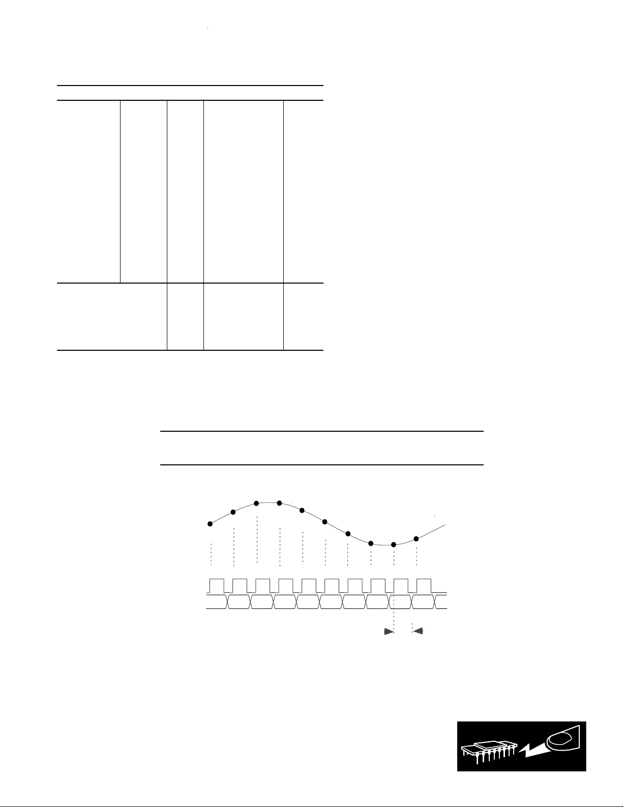
n+2
n+3
n+1
n
Analog
Input
clock
data
n-9 n-8 n-7 n-6 n-5 n-4 n-3 n-2 n-1
out
n+4
n+5
n+6
n+7
n+8
n+9
n
n+1
Tod = 7nsec typ
Figure 1. AD9244 Input Timing
CAUTION
ESD (electrostatic discharge) sensitive device. Electrostatic charges as high as 4000 V readily
accumulate on the human body and test equipment and can discharge without detection. Although
the AD9244 features proprietary ESD protection circuitry, permanent damage may occur on devices
subjected to high energy electrostatic discharges. Therefore, proper ESD precautions are recommended to avoid performance degradation or loss of functionality.
REV. PrD 01/22/02
–5–
WARNING!
ESD SENSITIVE DEVICE
Page 6
PRELIMINAR Y TECHNICAL DATA
AD9244–SPECIFICATIONS
PIN FUNCTION DESCRIPTIONS
Pin
Nunber Name Descriptions
1,2,5,32,33 AGND Analog Ground
3,4,31,34 AVDD Analog Supply Voltage
5 CLKGND Clock Ground
8,44 N C Do not connect
7,6 CLK+,CLK- Differential Clock Input
9 OEB Digital Output Enable (active low)
10 DB0 (LSB) Least Significant Bit, digital output
11-13,16-21
24-26 DB1 - DB12 Digital outputs
27 DB13 (MSB) Most Significant Bit, digital output
14,22,30 DRGND Digital Ground
15,23,29 DRVDD Digital Supply Voltage
28 OTR Out of range indicator (logic 1 indicates OTR)
35 DFS Data Format Select, connect to;
DRGND for straight binary
DRVDD for 2’s complement
36 REFSENSE Internal reference control
37 VREF Internal Reference
38 REFGND Reference ground
39,40,41,42 REFT,REFB Internal ADC reference decoupling
43 DUTY 50% Duty Cycle Restore, (Connect to AVDD to activate 50% duty cycle restore, de-
couple to AGND for external control of both clock edges.)
45 CML Common mode reference (0.5*AVDD)
46,47 V IN +,VIN- Differential analog inputs
48 VR Internal Bias Decoupling
AGND
AGND
AVDD
AVDD
AGND
CLK-
CLK+
NC
OEB
DB0 (LSB)
DB1
DB2
VR
VIN-
VIN+
CML
NC
DUTY
REFT
REFT
REFB
1
2
3
4
5
6
7
(Preliminary and not to scale)
8
9
10
11
12
13 14 15 16 17 18 19 20 21 22 23 24
DB3
DRGND
DRVDD
AD9244
48 LQFP
DB4
DB5
DB6
DB7
DB8
DB9
REFB
REFGND
VREF
373839404142434445464748
REF SENSE
36
DFS
35
AVDD
34
AGND
33
AGND
32
AVDD
31
30
DRGND
29
DRVDD
28
OTR
27
DB13 (MSB)
26
DB12
25
DB11
DRGND
DRVDD
DB10
REV. PrD 01/22/02
–6–
Page 7

PRELIMINAR Y TECHNICAL D A T A
AD9244–SPECIFICATIONS
DEFINITIONS OF SPECIFICATIONS
INTEGRAL NONLINEARITY (INL)
INL refers to the deviation of each individual code from a
line drawn from “negative full scale” through “positive
full scale.” The point used as “negative full scale” occurs
1/2 LSB before the first code transition. “Positive full
scale” is defined as a level 1 1/2 LSB beyond the last code
transition. The deviation is measured from the middle of
each particular code to the true straight line.
DIFFERENTIAL NONLINEARITY (DNL, NO MISSING
CODES)
An ideal ADC exhibits code transitions that are exactly 1
LSB apart. DNL is the deviation from this ideal value.
Guaranteed no missing codes to 14-bit resolution indicates
that all 16384 codes, respectively, must be present over all
operating ranges.
ZERO ERROR
The major carry transition should occur for an analog
value 1/2 LSB below VIN+ = VIN-. Zero error is defined
as the deviation of the actual transition from that point.
GAIN ERROR
The first code transition should occur at an analog value
1/2 LSB above negative full scale. The last transition
should occur at an analog value 1 1/2 LSB below the
nominal full scale. Gain error is the deviation of the actual
difference between first and last code transitions and the
ideal difference between first and last code transitions.
TEMPERATURE DRIFT
The temperature drift for zero error and gain error specifies the maximum change from the initial (+25°C) value
to the value at T
POWER SUPPLY REJECTION
The specification shows the maximum change in full scale
from the value with the supply at the minimum limit to the
value with the supply at its maximum limit.
APERTURE JITTER
The variation in aperture delay for successive samples
which is manifested as noise on the input to the A/D.
APERTURE DELAY
Aperture delay is a measure of the sample-and-hold amplifier (SHA) performance and is measured from the rising
edge of the clock input to when the input signal is held for
conversion.
MIN
or T
MAX
.
SIGNAL-TO-NOISE AND DISTORTION (S/N+D,
SINAD) RATIO
The ratio of the rms value of the measured input signal to
the rms sum of all other spectral components below the
Nyquist frequency, including harmonics but excluding dc.
The value for S/N+D is expressed in decibels.
EFFECTIVE NUMBER OF BITS (ENOB)
For a sine wave, SINAD can be expressed in terms of the
number of bits. Using the following formula,
N = (SINAD – 1.76)/6.02
it is possible to get a measure of performance expressed as
N, the effective number of bits.
Thus, effective number of bits for a device for sine wave
inputs at a given input frequency can be calculated directly
from its measured SINAD.
TOTAL HARMONIC DISTORTION (THD)
The ratio of the rms sum of the first six harmonic components to the rms value of the measured input signal and is
expressed as a percentage or in decibels.
SIGNAL-TO-NOISE RATIO (SNR)
The ratio of the rms value of the measured input signal to
the rms sum of all other spectral components below the
Nyquist frequency, excluding the first six harmonics and
dc. The value for SNR is expressed in decibels.
SPURIOUS FREE DYNAMIC RANGE (SFDR)
The difference in dB between the rms amplitude of the
input signal and the peak spurious signal.
NYQUIST SAMPLING
When the frequency components of the analog input are
below the Nyquist frequency (Fclock/2), this is often referred to as Nyquist sampling.
IF SAMPLING
Due to the effects of aliasing, an ADC is not necessarily
limited to Nyquist sampling. Higher sampled frequencies
will be aliased down into the 1st Nyquist zone (DCFclock/2) on the output of the ADC. Care must be taken
that the bandwidth of the sampled signal does not overlap
Nyquist zones and alias onto itself. Nyquist sampling performance is limited by the bandwidth of the input SHA
and clock jitter (jitter adds more noise at higher input
frequencies).
REV. PrD 01/22/02
–7–
Page 8

TYPICAL PERFORMANCE CHARACTERISTICS - AD9244
(AVDD = 5.0V, DRVDD = 3.0V, f
= 65MSPS with CLK Duty Cycle Stabilizer Enabled, TA =25
SAMPL E
°C, Differential Input Span,
, VCM = 2.5V, AIN = -0.5dBFS, VREF = 2.0V, FFT
length = 8K, unless otherwise noted)
TPC1. Single Tone 8K FFT, fIN = 5MHz TPC2. Single Tone SNR/SFDR vs AIN, fIN = 5MHz
TPC3. Single Tone 8K FFT, f
TPC5. 3rd Order Intermodulation Distortion vs.
Fin1,Fin2 at Ain1,Ain2=-6.5dBFS. Spacing between Fin1 and Fin2 = 1MHz.
= 31MHz TPC4. Dual-Tone SNR/SFDR vs. AIN with f
IN
REV. PrD 01/22/02
–8–
= 18MHz and f
TPC6. Single Tone SNR/SFDR vs AIN, f
= 20MHz
IN2
IN
IN1
= 31MHz
Page 9

TYPICAL PERFORMANCE CHARACTERISTICS - AD9244
(AVDD = 5.0V, DRVDD = 3.0V, f
length = 8K, unless otherwise noted)
TPC7. SINAD/ENOB vs. Frequency TPC10. SNR vs. Frequency
= 65MSPS with CLK Duty Cycle Stabilizer Enabled, TA =25
SAMPL E
°C, Differential Input Span,
, VCM = 2.5V, AIN = -0.5dBFS, VREF = 2.0V, FFT
TPC8. THD vs. Frequency TPC11. SFDR vs. Frequency
TPC9. SNR vs. Temperature and Frequency
REV. PrD 01/22/02
TPC12. THD vs. Temperature and Frequency
–9–
Page 10

TYPICAL PERFORMANCE CHARACTERISTICS - AD9244
(AVDD = 5.0V, DRVDD = 3.0V, f
length = 8K, unless otherwise noted)
TPC13. Harmonics vs. Frequency TPC16. SINAD vs. Sample Rate
= 65MSPS with CLK Duty Cycle Stabilizer Enabled, TA =25
SAMPL E
°C, Differential Input Span,
, VCM = 2.5V, AIN = -0.5dBFS, VREF = 2.0V, FFT
TPC14. SFDR vs. Sample Rate
TPC15. Typical INL TPC18. Typical DNL
REV. PrD 01/22/02
TPC17. SINAD/SFDR vs. Duty Cycle, , f
–10–
= 20MHz
IN
Page 11

TYPICAL PERFORMANCE CHARACTERISTICS - AD9244
(AVDD = 5.0V, DRVDD = 3.0V, f
= 65MSPS with CLK Duty Cycle Stabilizer Enabled, TA =25
SAMPL E
length = 8K, unless otherwise noted)
TPC19. Dual-Tone 8K FFT, f
= 45.6MHz
= 44.2MHz and f
IN1
IN2
°C, Differential Input Span,
TPC22. Dual Tone SNR and SFDR, f
and f
= 45.6MHz
IN2
, VCM = 2.5V, AIN = -0.5dBFS, VREF = 2.0V, FFT
IN1
= 44.2MHz
TPC20. Dual-Tone 8K FFT, f
70.6MHz
TPC21. Dual-Tone 8K FFT, f
and f
= 140.7MHz
IN2
REV. PrD 01/22/02
= 69.2MHz and f
IN1
= 139.2MHz
IN1
IN2
=
TPC23. Dual-Tone SNR and SFDR, f
and f
= 70.6MHz
IN2
TPC24. Dual-Tone SNR and SFDR, f
and f
= 140.7MHz
IN2
–11–
= 69.2MHz
IN1
= 139.2MHz
IN1
Page 12

TYPICAL PERFORMANCE CHARACTERISTICS - AD9244
(AVDD = 5.0V, DRVDD = 3.0V, f
length = 8K, unless otherwise noted)
= 65MSPS with CLK Duty Cycle Stabilizer Enabled, TA =25
SAMPL E
°C, Differential Input Span,
, VCM = 2.5V, AIN = -0.5dBFS, VREF = 2.0V, FFT
TPC25. Single Tone 8K FFT at IF = 190.82MHz
(typical WCDMA carrier), f
TPC26. Dual-Tone 8K FFT, f
= 61.44MSPS
SAMPLE
= 239.1MHz and f
IN1
IN2
240.7MHz
=
TPC28. Single Tone SNR and SFDR at IF = 190.82
MHz (typical WCDMA carrier), f
TPC29. Dual-Tone SNR and SFDR, f
and f
= 240.7MHz
IN2
= 61.44MSPS
SAMPLE
= 239.1MHz
IN1
TPC27. CMRR vs. Frequency (A
= 2.5V
REV. PrD 01/22/02
= 0dBFS and CML
IN
–12–
Page 13

TYPICAL PERFORMANCE CHARACTERISTICS - AD9244
AD9244 - SINAD/SFDR vs. AIN at FIN=190 MHz
95
90
85
80
75
70
dBFS and dBc
65
60
55
-24 -19 -14 -9 -4 1
AIN-dBFS
TPC30. Undersampling Performance of AD9244, f
CLK
AD9244 - SNR/SFDR v s. AIN at FIN=240 MHz
100
90
80
70
dBFS and dBc
60
50
SINAD-dBc
SINAD-dBFS
SFDR-dBc
SFDR-dBFS
=65MSPS, Driving ADC Inputs with Transformer and Balun
SNR-dBc
SNR-dBFS
SFDR-dBc
SFDR-dBFS
40
-24 -19 -14 -9 -4 1
AIN-dBFS
TPC31. Undersampling Performance of AD9244, f
CLK
AD9244 with FIN= 240 MHz and F
(2 V Input Span-Differential, Ain=-8.5 dBFS)
0
-10
-20
-30
-40
-50
-60
dBFs
-70
-80
-90
-100
-110
-120
0 4 8 121620242832
Frequency (MHz)
TPC32. Undersampling Performance of AD9244, Driving ADC Inputs with Transformer and Balun
=65MSPS, Driving ADC Inputs with Transformer and Balun
=65 MSPS
CLK
SNR=73 dBFS
THD=-89.5 dBFS
SINAD=72.7 dBFS
Note: Spur Floor Below 90
dBc @ 240 MHz!
REV. PrD 01/22/02
–13–
Page 14

AD9244
PRELIMINAR Y TECHNICAL DATA
THEORY OF OPERATION
The AD9244 is a high performance, single supply 14-bit
ADC. In addition to high dynamic range Nyquist sampling, it is designed for excellent IF undersampling performance with an input analog bandwidth of 750MHz.
The AD9244 utilizes an eight stage pipeline architecture
with a wideband, calibrated, input sample and hold amplifier (SHA) implemented on a cost-effective CMOS process. Each stage of the pipeline, excluding the last, consists of a low resolution flash ADC along with a switched
capacitor DAC and interstage residue amplifier (MDAC).
The MDAC amplifies the difference between the reconstructed DAC output and the flash input for the next stage
in the pipeline. One bit of redundancy is used in each of
the stages to facilitate digital correction of flash errors.
The last stage simply consists of a flash ADC.
The performance of the AD9244 is greatly enhanced by
the use of active calibration, yielding superb dynamic
performance.
The pipeline architecture allows a greater throughput rate
at the expense of pipeline delay or latency. While the converter captures a new input sample every clock cycle, it
takes eight clock cycles for the conversion to be fully processed and appear at the output. This is illustrated in Figure 1 on page 5. This latency is not a concern in many
applications. The digital output, together with the out-ofrange indicator (OTR), is latched into an output buffer to
drive the output pins. The output drivers of the AD9244
can be configured to interface with +5V or +3V logic
families.
Connecting the DUTY pin to AVDD implements the
internal clock stabilization function in the AD9244. In
this mode, the AD9244 generates its own internal falling
edge to create an internal 50% duty cycle clock, independent of the externally applied duty cycle. See the pin function descriptions on page 6 for details.
If the DUTY pin is connected to ground through a 10KΩ
resistor or left floating (and decoupled), the AD9244 will
use both edges of the external clock in its internal timing
circuitry (see Figure 1 and specification page for exact
timing requirements).
Control of straight binary or two’s complement output
format is accomplished with the DFS pin. See the pin
function descriptions on page 6 for details.
The ADC samples the analog input on the rising edge of
the clock. While clock is low, the input SHA is in sample
mode. When the clock transitions to a high logic level, the
SHA goes into the hold mode. System disturbances just
prior to or immediately after the rising edge of the clock
and/or excessive clock jitter may cause the input SHA to
acquire the wrong value, and should be minimized.
inputs to the VIN+ and VIN- pins results in a data inversion (complementing the output word).
S
C
H
-
+
C
H
S
VIN+
VIN-
C
PIN,PAR
C
PIN,PAR
S
S
C
S
H
C
S
Figure 2. Analog Input of AD9244 SHA
The optimum noise and dc linearity performance for either differential or single-ended inputs is achieved with the
largest input signal voltage span (i.e., 2V input span) and
matched input impedance for VIN+ and VIN-. Only a
slight degradation in dc linearity performance exists between the 2V and 1V input spans.
High frequency inputs may find the 1V span better suited
to achieve superior SFDR performance. (See Typical
Performance Characteristics.)
When the ADC is driven by an op amp and a capacitive
load is switched onto the output of the op amp, the output
will momentarily drop due to its effective output impedance. As the output recovers, ringing may occur. To remedy the situation, a series resistor can be inserted between
the op amp and the SHA input as shown in Figure 3. A
shunt capacitance also acts like a charge reservoir, sinking
or sourcing the additional charge required by the hold
capacitor, C
, further reducing current transients seen at
H
the op amp’s output.
V
CC
V
EE
10µF
R
S
33Ω
0.1µF
R
33Ω
AD9244
S
VIN+
15pF
VINVREF
REFSENSE
REFCOM
Figure 3. Resistors Isolating SHA Input from Op Amp
ANALOG INPUT OPERATION
Figure 2 shows the equivalent analog input of the AD9244
which consists of a 750 MHz differential SHA. The differential input structure of the SHA is flexible, allowing
the device to be configured for either a differential or
single-ended input. The analog inputs VIN+ and VINare interchangeable, with the exception that reversing the
REV. PrD 01/22/02
–14–
The optimum size of this resistor is dependent on several
factors, including the ADC sampling rate, the selected op
amp, and the particular application. In most applications,
a 30Ω to 100Ω resistor is sufficient.
Page 15

PRELIMINAR Y TECHNICAL DATA
For noise sensitive applications, the very high bandwidth
of the AD9244 may be detrimental and the addition of a
series resistor and/or shunt capacitor can help limit the
wideband noise at the ADC’s input by forming a low pass
filter. The source impedance driving VIN+ and VINshould be matched. Failure to provide matching may result in degradation of the SNR, THD, or SFDR of the
AD9244.
ANALOG INPUT AND REFERENCE OVERVIEW
The differential input span of the AD9244 is equal to the
potential at the VREF pin. The VREF potential may be
obtained from the internal AD9244 reference or an external source.
In differential applications, the center point of the input
span is obtained by the common mode level of the signals.
In single ended applications, the center point is the dc
potential applied to one input pin while the signal is applied to the opposite input pin.
Figure 4 is a simplified model of the AD9244 analog input, showing the relationship between the analog inputs,
VIN+, VIN-, and the reference voltage, VREF. Note that
this is only a symbolic model and that no actual negative
voltages exist inside the AD9244. Similar to the voltages
applied to the top and bottom of the resistor ladder in a
flash ADC, the value VREF/2 defines the minimum and
maximum input voltages to the ADC core.
AD9244
VIN+
VIN-
Figure 4. Equivalent Analog Input of AD9244
The addition of a differential input structure allows the
user to easily configure the inputs for either single-ended
or differential operation. The ADC’s input structure allows the dc offset of the input signal to be varied independently of the input span of the converter. Specifically, the
input to the ADC core can be defined as the difference of
the voltages applied at the VIN+ and VIN- input pins.
Therefore, the equation
V
defines the output of the differential input stage and pro-
vides the input to the ADC core.
The voltage, V
–VREF/2 < V
where VREF is the voltage at the VREF pin.
AD9244
+
Σ
-
V
CORE
+VREF/2
ADC
COR E
14
-VREF/2
= VIN+ – VIN- (1)
CORE
, must satisfy the condition,
CORE
< VREF/2 (2)
CORE
Table I. Analog Input Configuration Summary
Input Input Input Range (V)
Connection Coupling Span (V) VIN+
Single-Ended DC or AC 1.0 0.5 to 1.5 1.0 Best for stepped input response applications, requires ±5 V op amp.
2.0 1 to 3 2.0 Optimum noise performance for single ended mode, often
Differential DC or AC 1.0 2.25 to 2.75 2.75 to 2.25 Optimum full-scale THD and SFDR performance well beyond
(via Transformer) the ADC’s Nyquist frequency. Preferred mode for undersampling
or Amplifier applications.
2.0 2.0 to 3.0 3.0 to 2.0 Optimum noise performance for differential mode.
NOTE
1
VIN+ and VIN- can be interchanged if signal inversion is required.
1
Table II. Reference Configuration Summary
VIN-
1
Comments
requires low distortion op amp with VCC > +5 V due to its headroom issues.
Reference Input Span (VIN+–VIN-)
Operating Mode (V p-p) Required VREF (V) Connect T o
INTERNAL 1 1 REFSENSE VREF
INTERNAL 2 2 REFSENSE AGND
INTERNAL 1 ⱕ SPAN ⱕ 21 ⱕ VREF ⱕ 2.0 R1 VREF AND REFSENSE
(SPAN=VREF) VREF = (1 + R1/R2) R2
REFSENSE AND REFGND
EXTERNAL SPAN=EXTERNAL REF 1 ⱕ VREF ⱕ 2.0 REFSENSE AVDD
VREF EXTERNAL REF
REV. PrD 01/22/02
–15–
Page 16

AD9244
PRELIMINAR Y TECHNICAL DATA
In addition to the limitations placed on the input voltages
VIN+ and VIN- by Equation 2, boundaries on the inputs
also exist based on the power supply voltages according to
the conditions
AGND – 0.3V < VIN+ < AVDD + 0.3V
AGND – 0.3V < VIN- < AVDD + 0.3V
(3)
where AGND is nominally 0V and AVDD is nominally
+5 V. The range of valid inputs for VIN+ and VIN- is
any combination that satisfies both Equations 2 and 3.
For additional information showing the relationship between VIN+, VIN-, VREF and the analog input range of
the AD9244, see Tables I and II on page 15.
REFERENCE OPERATION
The AD9244 contains a bandgap reference which provides a pin-strappable option to generate either a 1V or
2V output. With the addition of two external resistors, the
user can generate reference voltages between 1V and 2V.
Another alternative is to use an external reference for designs requiring enhanced accuracy and/or drift performance as described later in this section. Figure 5a shows a
simplified model of the internal voltage reference of the
AD9244. A reference amplifier buffers a 1V fixed reference. The output from the reference amplifier, A1, appears on the VREF pin. As stated earlier, the voltage on
the VREF pin determines the full scale differential input
span of the ADC.
The voltage appearing at the VREF pin, and the state of
the internal reference amplifier, A1, are determined by the
voltage present at the REFSENSE pin. The logic circuitry contains comparators that monitor the voltage at the
REFSENSE pin. If REFSENSE is tied to AGND, the
switch is connected to the internal resistor network thus
providing a VREF of 2.0V. If REFSENSE is tied to
VREF pin via a short or resistor, the switch will connect
to the REFSENSE pin. This connection will provide a
VREF of 1.0V. An external resistor network will provide
an alternative VREF between 1.0V and 2.0V (see Figure
6). Another comparator controls internal circuitry which
disables the reference amplifier if REFSENSE is tied to
AVDD. Disabling the reference amplifier allows the
VREF pin to be driven by an external voltage reference.
The actual reference voltages used by the internal circuitry
of the AD9244 appear on the REFT and REFB pins. The
voltages on these pins are symmetrical about the analog
supply. For proper operation when using an internal or
external reference, it is necessary to add a capacitor network to decouple these pins. Figure 5b shows the recommended decoupling network. The turn-on time of the
reference voltage appearing between REFT and REFB is
approximately 10ms and should be evaluated in any power
down mode of operation.
USING THE INTERNAL REFERENCE
The AD9244 can be easily configured for either a 1V p-p
differential input span or 2V p-p input span by setting the
internal reference. Other input spans can be realized with
two external gain-setting resistors as shown in Figure 6 of
this data sheet, or using an external reference.
REV. PrD 01/22/02
–16–
AD9244
TO
ADC
REFT
A2
2.5V
REFB
VREF
REFSENSE
REFGND
1V
DISAB LE
A1
A1
LOGIC
Figure 5a. AD9244 Equivalent Reference Circuit
0.1µF
VREF REF T
10µF0.1µF
AD9244
REFB
0.1µF10µF
0.1µF
Figure 5b. REFT and REFB Decoupling
Pin Programmable Reference
By shorting the VREF pin directly to the REFSENSE
pin, the internal reference amplifier is placed in a unity
gain mode and the resultant VREF output is 1V. By shorting the REFSENSE pin directly to the REFGND pin, the
internal reference amplifier is configured for a gain of 2.0
and the resultant VREF output is 2.0V. The VREF pin
should be bypassed to the REFGND pin with a 10µF
tantalum capacitor in parallel with a low-inductance
0.1µF ceramic capacitor as shown in Figure 6.
Resistor Programmable Reference
Figure 6 shows an example of how to generate a reference
voltage other than 1.0V or 2.0V with the addition of two
external resistors. Use the equation,
VREF = 1V ×(1 + R1/R2)
to determine appropriate values for R1 and R2. These
resistors should be in the 2KΩ to 10KΩ range. For the
example shown, R1 equals 2.5KΩ and R2 equals 5KΩ.
From the equation above, the resultant reference voltage
on the VREF pin is 1.5 V. This sets the differential input
span to be 1.5V p-p. The midscale voltage can also be set
to VREF by connecting VIN- to VREF.
3.25V
1.75V
2.5V
10µF0.1µF
33Ω
33Ω
R1
2.5K
R2
5K
15pF
1.5V
AD9244
VIN+
VINVREF
REFSENSE
REFGND
REFT
REFB
0.1µF
0.1µF
0.1µF
10µF
Figure 6. Resistor Programmable Reference (1.5V p-p
Input Span, Differential Input with VCM = 2.5V
Page 17

PRELIMINAR Y TECHNICAL D A TA
OUTLINE DIMENSIONS
Dimensions shown in inches and (mm).
48 pin LQFP package
(ST-48)
AD9244
0.063 (1.60) MAX
0.030 (0.75)
0.018 (0.45)
SEATING
0.006 (0.15)
PLANE
0.002 (0.05)
COPLANARITY (0.08)
0° - 7°
0.057 (1.45)
0.053 (1.35)
0° MIN
0.007 (0.2)
0.004 (0.09)
0.354 (9.00) BSC
0.276 (7.0) BSC
48
1
TOP VIEW
(PINS DOWN)
12
13
0.019 (0.5)
BSC
37
24
0.011 (0.27)
0.006 (0.17)
36
0.354
0.276
(9.00)
(7.0)
BSC
BSC
25
REV. PrD 01/22/02
17
 Loading...