

Page 1
Quad, 12-Bit, 170 MSPS/210 MSPS/250 MSPS
A
www.BDTIC.com/ADI
FEATURES
4 ADCs in 1 package
Coded serial digital outputs with ECC per channel
On-chip temperature sensor
−95 dB channel-to-channel crosstalk
SNR = 65 dBFS with AIN = 85 MHz at 250 MSPS
SFDR = 77 dBc with AIN = 85 MHz at 250 MSPS
Excellent linearity
DNL = ±0.3 LSB (typical)
INL = ±0.7 LSB (typical)
780 MHz full power analog bandwidth
Power dissipation = 380 mW per channel at 250 MSPS
1.25 V p-p input voltage range, adjustable up to 1.5 V p-p
1.8 V supply operation
Clock duty cycle stabilizer
Serial port interface features
Power-down modes
Digital test pattern enable
Programmable header
Programmable pin functions (PGMx, PDWN)
APPLICATIONS
Communication receivers
Cable head end equipment/M-CMTS
Broadband radios
Wireless infrastructure transceivers
Radar/military-aerospace subsystems
Test equipment
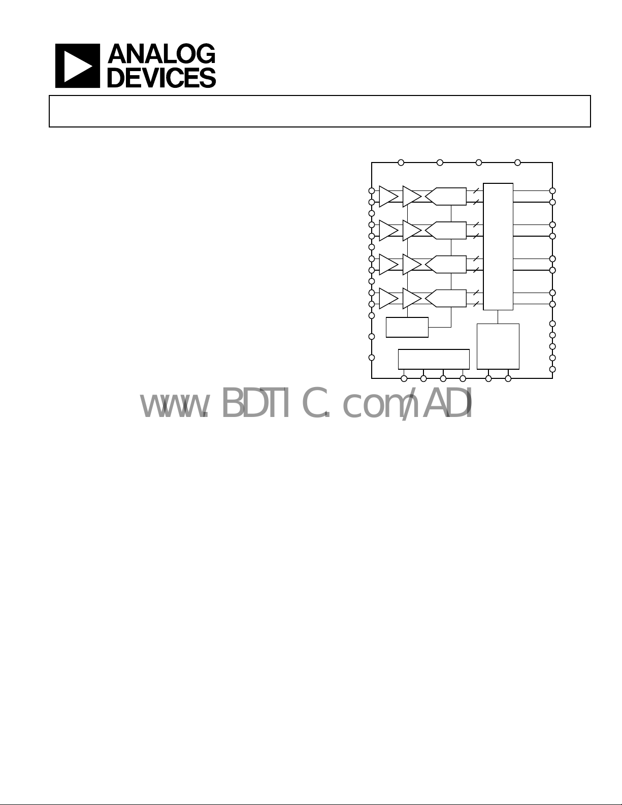
Serial Output 1.8 V ADC
AD9239
FUNCTIONAL BLOCK DIAGRAM
VDD PDWN DRVDD DRGND
AD9239
VIN + A DOUT + A
VIN – A
VCM A
VIN + B
VIN – B
VCM B
VIN + C DOUT + C
VIN – C
VCM C
VIN + D
VIN – D
VCM D
RBIAS
TEMPOUT
BUF
BUF
BUF
BUF
REFERENCE
SCLK SDI/
SHA
SHA
SHA
SHA
SDIO
PIPELINE
PIPELINE
PIPELINE
PIPELINE
SERIAL
PORT
ADC
ADC
ADC
ADC
SDO CSB
Figure 1.
12
12
12
12
DATA RATE
MULTIPLIER
CLK+ CLK–
CML DRIVERS
DATA SERIALIZE R, ENCODER, AND
CHANNEL A
CHANNEL B
CHANNEL C
CHANNEL D
DOUT – A
DOUT + B
DOUT – B
DOUT – C
DOUT + D
DOUT – D
PGM3
PGM2
PGM1
PGM0
RESET
06980-001
GENERAL DESCRIPTION
The AD9239 is a quad, 12-bit, 250 MSPS analog-to-digital
converter (ADC) with an on-chip temperature sensor and a
high speed serial interface. It is designed to support digitizing
high frequency, wide dynamic range signals with an input
bandwidth up to 780 MHz. The output data are serialized and
presented in packet format, consisting of channel-specific
information, coded samples, and error correction code.
The ADC requires a single 1.8 V power supply and the input
clock may be driven differentially with a sine wave, LVPECL,
TTL, or LVDS. A clock duty cycle stabilizer allows high
performance at full speed with a wide range of clock duty
cycles. The on-chip reference eliminates the need for external
decoupling and can be adjusted by means of SPI control.
Various power-down and standby modes are supported. The
ADC typically consumes 145 mW per channel with the digital
link still in operation when standby operation is enabled.
Rev. 0
Information furnished by Analog Devices is believed to be accurate and reliable. However, no
responsibility is assumed by Analog Devices for its use, nor for any infringements of patents or other
rights of third parties that may result from its use. Specifications subject to change without notice. No
license is granted by implication or otherwise under any patent or patent rights of Analog Devices.
Trademarks and registered trademarks are the property of their respective owners.
Fabricated on an advanced CMOS process, the AD9239 is available in a Pb-free/RoHS-compliant, 72-lead LFCSP package. It is
specified over the industrial temperature range of −40°C to +85°C.
PRODUCT HIGHLIGHTS
1. Four ADCs are contained in a small, space-saving package.
2. An on-chip PLL allows users to provide a single ADC
sampling clock, and the PLL distributes and multiplies up
to produce the corresponding data rate clock.
3. Coded data rate supports up to 4.0 Gbps per channel.
Coding includes scrambling to ensure proper dc common
mode, embedded clock, and error correction.
4. The AD9239 operates from a single 1.8 V power supply.
5. Flexible synchronization schemes and programmable
mode pins.
6. On-chip temperature sensor.
One Technology Way, P.O. Box 9106, Norwood, MA 02062-9106, U.S.A.
Tel: 781.329.4700 www.analog.com
Fax: 781.461.3113 ©2008 Analog Devices, Inc. All rights reserved.
Page 2

AD9239
www.BDTIC.com/ADI
TABLE OF CONTENTS
Features .............................................................................................. 1
Applications ....................................................................................... 1
Functional Block Diagram .............................................................. 1
General Description ......................................................................... 1
Product Highlights ........................................................................... 1
Revision History ............................................................................... 2
Specifications ..................................................................................... 3
AC Specifications .......................................................................... 4
Digital Specifications ................................................................... 5
Switching Specifications .............................................................. 6
Timing Diagram ........................................................................... 7
Absolute Maximum Ratings ............................................................ 8
Thermal Resistance ...................................................................... 8
ESD Caution .................................................................................. 8
Pin Configuration and Function Description .............................. 9
Typical Performance Characteristics ........................................... 11
Equivalent Circuits ......................................................................... 17
Theory of Operation ...................................................................... 19
Analog Input Considerations ................................................... 19
Clock Input Considerations ...................................................... 21
Serial Port Interface (SPI) .............................................................. 31
Hardware Interface ..................................................................... 31
Memory Map .................................................................................. 33
Reading the Memory Map Table .............................................. 33
Reserved Locations .................................................................... 33
Default Values ............................................................................. 33
Logic Levels ................................................................................. 33
Outline Dimensions ....................................................................... 38
Ordering Guide .......................................................................... 38
REVISION HISTORY
10/08—Revision 0: Initial Version
Rev. 0 | Page 2 of 40
Page 3

AD9239
www.BDTIC.com/ADI
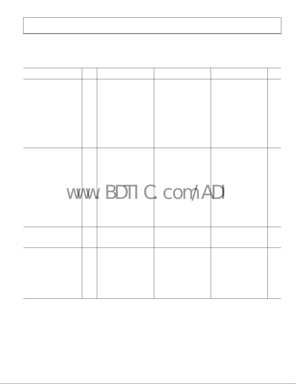
SPECIFICATIONS
AVDD = 1.8 V, DRVDD = 1.8 V, T
otherwise noted.
Table 1.
AD9239BCPZ-170 AD9239BCPZ-210 AD9239BCPZ-250
Parameter
1
Temp Min Typ Max Min Typ Max Min Typ Max Unit
RESOLUTION 12 12 Bits
ACCURACY
No Missing Codes Full Guaranteed Guaranteed Guaranteed
Offset Error 25°C −2 ±12 −2 ±12 −2 ±12 mV
Offset Matching 25°C 4 12 4 12 4 12 mV
Gain Error 25°C −2.8 +1 +4.7 −2.8 +1 +4.7 −2.8 +1 +4.7 % FS
Gain Matching 25°C 0.9 2.7 0.9 2.7 0.9 2.7 % FS
Differential Nonlinearity (DNL) Full ±0.28 ±0.6 ±0.28 ±0.6 ±0.3 ±0.6 LSB
Integral Nonlinearity (INL) Full ±0.45 ±0.9 ±0.7 ±1.3 ±0.7 ±1.3 LSB
ANALOG INPUTS
Differential Input Voltage Range
Common-Mode Voltage Full 1.4 1.4 1.4 V
Input Capacitance 25°C 2 2 2 pF
Input Resistance Full 4.3 4.3
Analog Bandwidth, Full Power Full 780 780 780 MHz
Voltage Common Mode (VCMx)
Voltage Output Full 1.4 1.44 1.5 1.4 1.44 1.5 1.4 1.44 1.5 V
Current Drive Full 1 1 1 mA
Temperature Sensor Output −1.12 −1.12 −1.12 mV/°C
Voltage Output Full 739 737 734 mV
Current Drive Full 10 10 10 µA
POWER SUPPLY
AVDD Full 1.7 1.8 1.9 1.7 1.8 1.9 1.7 1.8 1.9 V
DRVDD Full 1.7 1.8 1.9 1.7 1.8 1.9 1.7 1.8 1.9 V
I
Full 535 570 610 650 725 775 mA
AVDD
I
Full 98 105 111 120 123 133 mA
DRVDD
Total Power Dissipation
(Including Output Drivers)
Power-Down Dissipation Full 3 3 3 mW
Standby Dissipation
2
Full 152 173 195 mW
CROSSTALK Full −95 −95 −95 dB
Overrange Condition
1
See the AN-835 Application Note, Understanding High Speed ADC Testing and Evaluation, for definitions and details on how these tests were completed.
2
AVDD/DRVDD, with link established.
3
Overrange condition is specified with 6 dB above the full-scale input range.
3
Full −90 −90 −90 dB
= −40°C, T
MIN
2
Full 1.25 1.25 1.25 V p-p
= +85°C, 1.25 V p-p differential input, AIN = −1.0 dBFS, DCS enabled, unless
MAX
4.3
kΩ
Full 1.139 1.215 1.298 1.386 1.526 1.634 W
Rev. 0 | Page 3 of 40
Page 4

AD9239
www.BDTIC.com/ADI
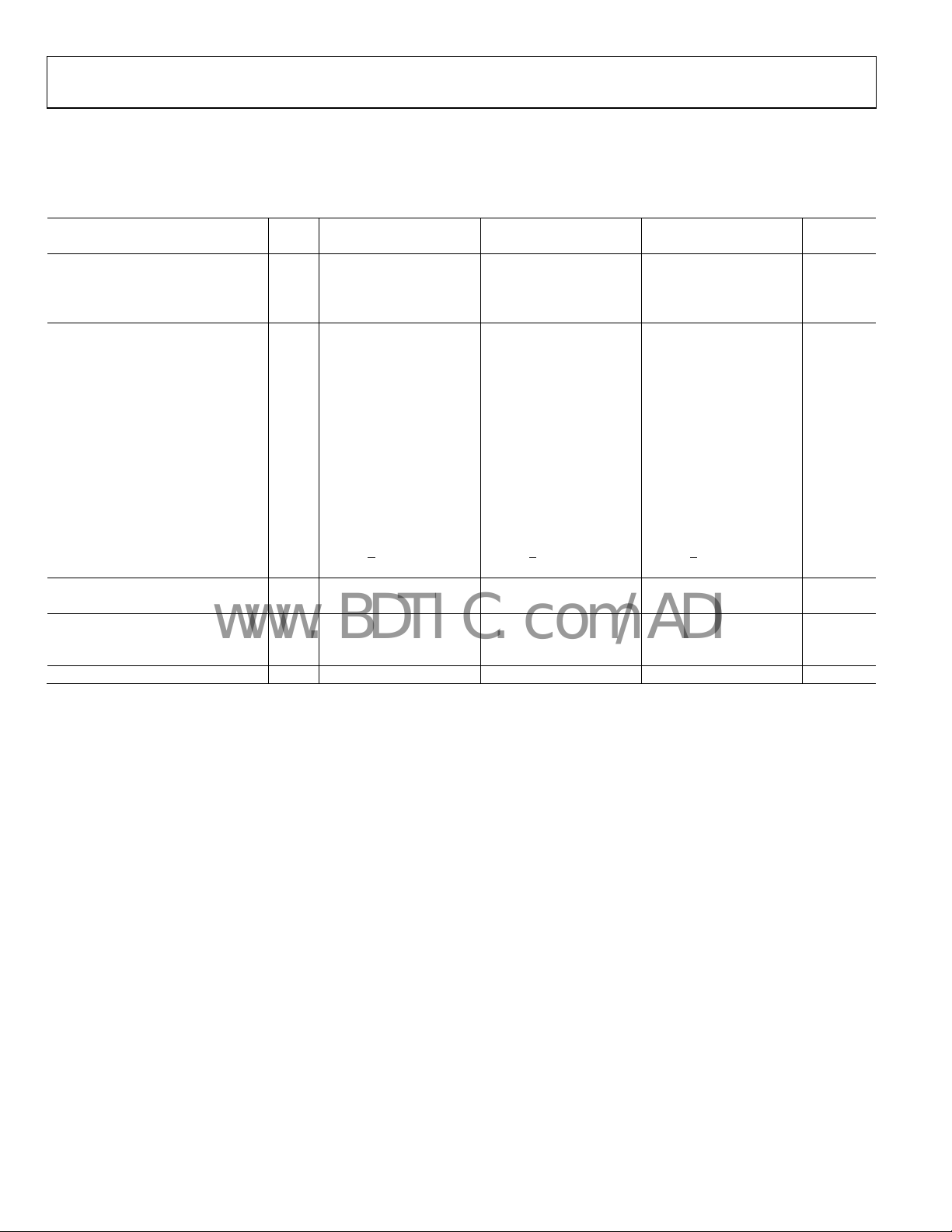
AC SPECIFICATIONS
AVDD = 1.8 V, DRVDD = 1.8 V, T
otherwise noted.
Table 2.
AD9239BCPZ-170 AD9239BCPZ-210 AD9239BCPZ-250
Parameter
1
Temp Min Typ Max Min Typ Max Min Typ Max Unit
SIGNAL-TO-NOISE RATIO (SNR)
fIN = 9.7 MHz 25°C 64.5 dB
fIN = 84.3 MHz Full 63.5 64.5 63.2 64.2 63.1 64.1 dB
fIN = 170.3 MHz 25°C 63.9 dB
fIN = 240.3 MHz 25°C 64.1 63.2 63.3 dB
SIGNAL-TO-NOISE RATIO (SINAD)
fIN = 9.7 MHz 25°C 64.2 dB
fIN = 84.3 MHz Full 63.3 64.4 62.8 63.9 62.8 63.8 dB
fIN = 170.3 MHz 25°C 63.1 dB
fIN = 240.3 MHz 25°C 63.9 63 63.1 dB
EFFECTIVE NUMBER OF BITS (ENOB)
fIN = 9.7 MHz 25°C 10.4 Bits
fIN = 84.3 MHz Full 10.2 10.4 10.1 10.3
fIN = 170.3 MHz 25°C 10.2 Bits
fIN = 240.3 MHz 25°C 10.3 10.2 10.2 Bits
WORST HARMONIC (SECOND)
fIN = 9.7 MHz 25°C 90 dBc
fIN = 84.3 MHz Full 87.5 78.6 86 77 86 74.5 dBc
fIN = 170.3 MHz 25°C 76 dBc
fIN = 240.3 MHz 25°C 82 80 82 dBc
WORST HARMONIC (THIRD)
fIN = 9.7 MHz 25°C 78 dBc
fIN = 84.3 MHz Full 79 74 76 72.6 76 72.5 dBc
fIN = 170.3 MHz 25°C 74 dBc
fIN = 240.3 MHz 25°C 84 77 80 dBc
WORST OTHER (EXCLUDING SECOND OR THIRD)
fIN = 9.7 MHz 25°C 85 dBc
fIN = 84.3 MHz Full 96 86 90 83.7 94 83.6 dBc
fIN = 170.3 MHz 25°C 85 dBc
fIN = 240.3 MHz 25°C 88 88 85 dBc
TWO-TONE INTERMOD DISTORTION (IMD)
f
= 140.2 MHz, f
IN1
= 141.3 MHz,
IN2
AIN1 and AIN2 = −7.0 dBFS
f
= 170.2 MHz, f
IN1
= 171.3 MHz,
IN2
AIN1 and AIN2 = −7.0 dBFS
1
See the AN-835 Application Note, Understanding High Speed ADC Testing and Evaluation, for definitions and details on how these tests were completed.
2
Tested at 210 MSPS and 250 MSPS only.
MIN
2
= −40°C, T
= +85°C, 1.25 V p-p differential input, AIN = −1.0 dBFS, DCS enabled, unless
MAX
10.1
10.3 Bits
4
25°C 78 77 76 dBc
25°C 77 76 dBc
Rev. 0 | Page 4 of 40
Page 5
AD9239
www.BDTIC.com/ADI
DIGITAL SPECIFICATIONS
AVDD = 1.8 V, DRVDD = 1.8 V, T
otherwise noted.
Table 3.
AD9239BCPZ-170 AD9239BCPZ-210 AD9239BCPZ-250
Parameter
CLOCK INPUTS (CLK+, CLK–)
LOGIC INPUTS (PDWN, CSB, SDI/
LOGIC OUTPUTS (SDO)
DIGITAL OUTPUTS
1
See the AN-835 Application Note, Understanding High Speed ADC Testing and Evaluation, for definitions and details on how these tests were completed.
2
Specified for 13 SDI/SDIO pins sharing the same connection.
1
Logic Compliance Full LVPECL/LVDS/CMOS LVPECL/LVDS/CMOS LVPECL/LVDS/CMOS
Differential Input Voltage Full 0.2 6 0.2 6 0.2 6 V p-p
Input Voltage Range Full AVDD −
Internal Common-Mode Bias Full 1.2 1.2 1.2 V
Input Common-Mode Voltage Full 1.1 AVDD 1.1 AVDD 1.1 AVDD V
High Level Input Voltage (VIH) Full 1.2 3.6 1.2 3.6 1.2 3.6 V
Low Level Input Voltage (VIL) Full 0 0.8 0 0.8 0 0.8 V
High Level Input Current (IIH) Full −10 +10 −10 +10 −10 +10 µA
Low Level Input Current (IIL) Full −10 +10 −10 +10 −10 +10 µA
Differential Input Resistance 25°C 16 20 24 16 20 24 16 20 24 kΩ
Input Capacitance 25°C 4 4 4 pF
2
SDIO, SCLK, RESET, PGMx)
Logic 1 Voltage Full 0.8 ×
Logic 0 Voltage Full 0.2 ×
Logic 1 Input Current (CSB) Full 0 0 0 µA
Logic 0 Input Current (CSB) Full −60 −60 −60 µA
Logic 1 Input Current
(SCLK, PDWN, SDI/SDIO,
RESET, PGMx)
Logic 0 Input Current
(SCLK, PDWN, SDI/SDIO,
RESET, PGMx)
Input Resistance 25°C 30 30 30 kΩ
Input Capacitance 25°C 4 4 4 pF
Logic 1 Voltage Full 1.2 AVDD +
Logic 0 Voltage Full 0 0.3 0 0.3 0 0.3 V
(DOUT + x, DOUT − x)
Logic Compliance Current
Differential Output Voltage Full 0.8 0.8 0.8 V
Common-Mode Level Full DRVDD/2 DRVDD/2 DRVDD/2 V
= −40°C, T
MIN
Temp Min Typ Max Min Typ Max Min Typ Max Unit
0.3
AVDD
Full 55 55 55 µA
Full 0 0 0 µA
= +85°C, 1.25 V p-p differential input, AIN = −1.0 dBFS, DCS enabled, unless
MAX
AVDD +
1.6
0.8 ×
AVDD
0.3
Current
mode
logic
AVDD −
0.3
AVDD
0.2 ×
1.2 AVDD +
AVDD +
1.6
0.8 ×
AVDD
0.3
Current
mode
logic
AVDD −
0.3
AVDD
0.2 ×
1.2 AVDD +
AVDD +
V
mode
logic
1.6
V
V
AVDD
V
0.3
Rev. 0 | Page 5 of 40
Page 6
AD9239
www.BDTIC.com/ADI
SWITCHING SPECIFICATIONS
AVDD = 1.8 V, DRVDD = 1.8 V, T
otherwise noted.
Table 4.
AD9239BCPZ-170 AD9239BCPZ-210 AD9239BCPZ-250
Parameter
CLOCK
DATA OUTPUT PARAMETERS
TERMINATION CHARACTERISTICS
APERTURE
OUT-OF-RANGE RECOVERY TIME 25°C 1 1 1 CLK cycles
1
See the AN-835 Application Note, Understanding High Speed ADC Testing and Evaluation, for definitions and details on how these tests were completed.
2
Receiver dependent.
3
See the section. Digital Start-Up Sequence
1
Clock Rate Full 170 100 210 100 250 100 MSPS
Clock Pulse Width High (tEH) Full 2.65 2.9 2.15 2.4 1.8 2.0 ns
Clock Pulse Width Low (tEL) Full 2.65 2.9 2.15 2.4 1.8 2.0 ns
Data Output Period or UI
(DOUT + x, DOUT − x)
Data Output Duty Cycle 25°C 50 50 50 %
Data Valid Time 25°C 0.8 0.8 0.8 UI
PLL Lock Time (t
Wake-Up Time (Standby) 25°C 250 250 250 ns
Wake-Up Time (Power-Down)
Pipeline Latency Full 40 40 40 CLK cycles
Data Rate per Channel (NRZ) 25°C 2.72 3.36 4.0 Gbps
Deterministic Jitter 25°C 10 10 10 ps max
Random Jitter 25°C 6 6 6 ps rms
Channel-to-Channel Bit Skew 25°C 0 0 0 sec
Channel-to-Channel Packet Skew
Output Rise/Fall Time 25°C 50 50 50 ps
Differential Termination Resistance 25°C 100 100 100 Ω
Aperture Delay (tA) 25°C 1.2 1.2 1.2 ns
Aperture Uncertainty (Jitter) 25°C 0.2 0.2 0.2 ps rms
) 25°C 4 4 4 µs
LOCK
2
= −40°C, T
MIN
Temp Min Typ Max Min Typ Max Min Typ Max Unit
Full 1/(16 × f
25°C 50 50 50 s
3
25°C +1 +1 +1 CLK cycles
= +85°C, 1.25 V p-p differential input, AIN = –1.0 dBFS, DCS enabled, unless
MAX
) 1/(16 × f
CLK
) 1/(16 × f
CLK
) sec
CLK
Rev. 0 | Page 6 of 40
Page 7
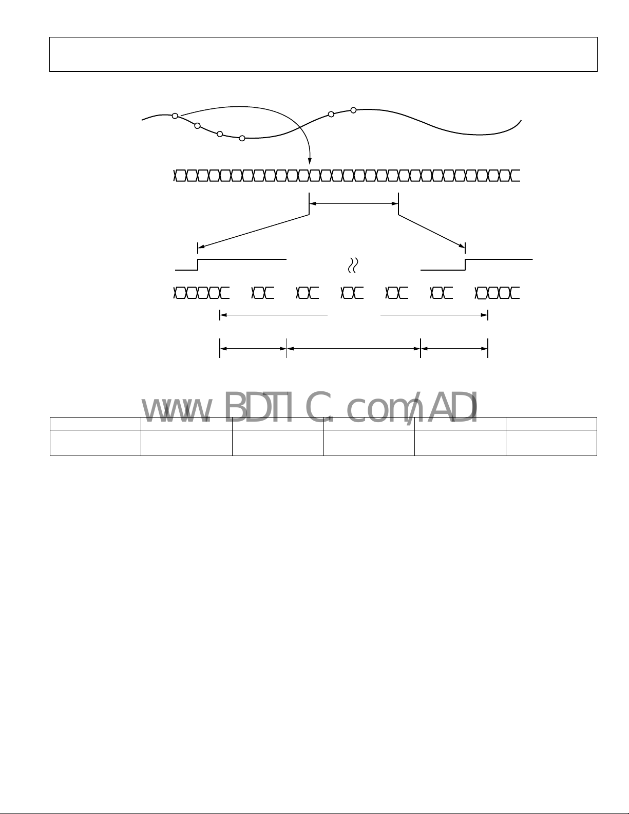
AD9239
www.BDTIC.com/ADI
TIMING DIAGRAM
SAMPLE
N + 1
N
ANALOG
INPUT SIGNAL
RATE CLOCK
SAMPLE
N – 40
N – 39
N – 38
N – 37
SAMPLE
RATE CLOCK
SERIAL
DATA OUT
SERIAL CODED SAMPLES: N – 40, N – 39, N – 38, N – 37 ...
... ... ...
8-BIT HEADER
CHANNEL ID
Figure 2. Timing Diagram
...
DATA PACKET 1
(64 BITS)
48-BIT ADC
DATA-WORD
...
...... ...
8-BIT ERROR
CORRECTION
06980-002
Table 1. Packet Protocol
Bits[64:57] Bits[56:45] Bits[44:33] Bits[32:21] Bits[20:9] Bits[8:1]
Header Data 1 Data 2 Data 3 Data 4 ECC
(8 bits MSB first) (12 bits MSB first) (12 bits MSB first) (12 bits MSB first) (12 bits MSB first) (8 bits MSB first)
Rev. 0 | Page 7 of 40
Page 8
AD9239
www.BDTIC.com/ADI
ABSOLUTE MAXIMUM RATINGS
Table 5.
Parameter Rating
Electrical
AVDD to AGND −0.3 V to +2.0 V
DRVDD to DRGND −0.3 V to +2.0 V
AGND to DRGND −0.3 V to +0.3 V
AVDD to DRVDD −2.0 V to +2.0 V
DOUT ± x to DRGND −0.3 V to DRVDD + 0.3 V
SDO, SDI/SDIO, CLK± , VIN ± x,
VCMx, TEMPOUT, RBIAS to AGND
SCLK, CSB, PGMx, RESET,
PDWN to AGND
Environmental
Storage Temperature Range −65°C to +125°C
Operating Temperature Range −40°C to +85°C
Lead Temperature
(Soldering 10 sec)
Junction Temperature 150°C
Stresses above those listed under Absolute Maximum Ratings
may cause permanent damage to the device. This is a stress
rating only; functional operation of the device at these or any
other conditions above those indicated in the operational
section of this specification is not implied. Exposure to absolute
maximum rating conditions for extended periods may affect
device reliability.
−0.3 V to AVDD + 0.3 V
−0.3 V to AVDD + 0.3 V
300°C
THERMAL RESISTANCE
The exposed paddle must be soldered to the ground plane for
the LFCSP package. Soldering the exposed paddle to the customer
board increases the reliability of the solder joints, maximizing
the thermal capability of the package.
Table 6. Thermal Resistance
Package Type θJA θJB θJC Unit
72-Lead LFCSP (CP-72-3) 16.2 7.9 0.6 °C/W
Typical θJA, θJB, and θJC values are specified for a 4-layer board in
still air. Airflow increases heat dissipation, effectively reducing
θ
. In addition, metal in direct contact with the package leads
JA
from metal traces and through holes, ground, and power planes
reduces the θ
.
JA
ESD CAUTION
Rev. 0 | Page 8 of 40
Page 9
AD9239
www.BDTIC.com/ADI
PIN CONFIGURATION AND FUNCTION DESCRIPTION
NC
AVDD
VCM C
AVDD
VIN – C
VIN + C
AVDD
AVDD
AVDDNCAVDD
AVDD
AVDD
VIN + B
VIN – B
AVDD
VCM B
AVDD
NC
TEMPOUT
RBIAS
AVDD
NC
NC
AVDD
VCM D
AVDD
VIN – D
VIN + D
AVDD
AVDD
AVDD
AVDD
CLK–
7271706968676665646362616059585756
1
2
3
4
5
6
7
8
9
10
11
12
13
14
15
16
17CLK+
18AVDD
PIN 1
INDICAT OR
PIN 0 = EPAD = AGND
AD9239
TOP VIEW
(Not to Scale)
55
54
NC
53
PGM0
52
PGM1
51
PGM2
50
PGM3
49
NC
48
AVDD
47
VCM A
46
AVDD
45
VIN – A
44
VIN + A
43
AVDD
42
AVDD
41
AVDD
40
CSB
39
SCLK
38
SDI/SDIO
37
SDO
192021222324252627282930313233
NC
AVDD
AVDD
RESET
DRVDD
DRGND
DOUT – D
DOUT – C
DOUT + D
DOUT + C
NOTES
1. NC = NO CONNECT .
2. THE EXPO SED PADDLE MUST BE SOLDERED T O THE GRO UND PLANE
FOR THE L FCSP PACKAGE. SOLDERING THE EXPOSED PADDLE TO
THE CUSTOMER BOARD INCREASES T HE RELIABIL ITY OF THE SOL DER
JOINTS, MAXIMIZ ING THE THERMAL CAPABILITY O F THE PACKAGE.
DOUT + B
DOUT – B
34
35PDWN
36NC
DRVDD
DRGND
DOUT – A
DOUT + A
06980-004
Figure 3. Pin Configuration
Table 7. Pin Function Descriptions
Pin No. Mnemonic Description
0 AGND Analog Ground (Exposed Paddle).
23, 34 DRGND Digital Output Driver Ground.
4, 7, 9, 12, 13, 14,
AVDD 1.8 V Analog Supply.
15, 18, 20, 21, 41, 42,
43, 46, 48, 55, 57,
60, 61, 62, 64, 65,
66, 69, 71
24, 33 DRVDD 1.8 V Digital Output Driver Supply.
2 TEMPOUT Output Voltage to Monitor Temperature.
3 RBIAS External Resistor to Set the Internal ADC Core Bias Current.
8 VCM D Common-Mode Output Voltage Reference (0.5 × AVDD).
10 VIN − D ADC D Analog Complement.
11 VIN + D ADC D Analog True.
16 CLK− Input Clock Complement.
17 CLK+ Input Clock True.
22 RESET Digital Output Timing Reset.
25 DOUT + D ADC D True Digital Output.
26 DOUT − D ADC D Complement Digital Output.
27 DOUT + C ADC C True Digital Output.
28 DOUT − C ADC C Complement Digital Output.
29 DOUT + B ADC B True Digital Output.
30 DOUT − B ADC B Complement Digital Output.
31 DOUT + A ADC A True Digital Output.
32 DOUT − A ADC A Complement Digital Output.
35 PDWN Power-Down.
Rev. 0 | Page 9 of 40
Page 10

AD9239
www.BDTIC.com/ADI
Pin No. Mnemonic Description
37 SDO Serial Data Output. Used for 4-wire SPI interface.
38 SDI/SDIO Serial Data Input/Serial Data IO for 3-Wire SPI Interface.
39 SCLK Serial Clock.
40 CSB Chip Select Bar.
44 VIN + A ADC A Analog Input True.
45 VIN − A ADC A Analog Input Complement.
47 VCM A Common-Mode Output Voltage Reference (0.5 × AVDD).
50 PGM3 Optional Pin to be Programmed by Customer.
51 PGM2 Optional Pin to be Programmed by Customer.
52 PGM1 Optional Pin to be Programmed by Customer.
53 PGM0 Optional Pin to be Programmed by Customer.
56 VCM B Common-Mode Output Voltage Reference (0.5 × AVDD).
58 VIN − B ADC B Analog Input Complement.
59 VIN + B ADC B Analog Input True.
67 VIN + C ADC C Analog Input True.
68 VIN − C ADC C Analog Input Complement.
70 VCM C Common-Mode Output Voltage Reference (0.5 × AVDD).
1, 5, 6, 19, 36,
49, 54, 63, 72
NC No Connection.
Rev. 0 | Page 10 of 40
Page 11
AD9239
www.BDTIC.com/ADI
TYPICAL PERFORMANCE CHARACTERISTICS
0
AIN = –1.0dBF S
SNR = 64.88dB
ENOB = 10.49 BI TS
–20
SFDR = 77.57d Bc
–20
0
AIN = –1.0dBFS
SNR = 63.13dB
ENOB = 10.19 BI TS
SFDR = 76.07dBc
–40
–60
–80
AMPLITUDE (dBFS)
–100
–120
0 10 20304050607080
FREQUENCY (MHz)
Figure 4. Single-Tone 32k FFT with fIN = 84.3 MHz, f
0
AIN = –1.0dBF S
SNR = 63.95dB
ENOB = 10.33 BI TS
–20
SFDR = 78.90dBc
–40
–60
–80
AMPLITUDE (dBFS)
–100
= 170 MSPS
SAMPLE
–40
–60
–80
AMPLITUDE (dBFS)
–100
–120
020406080100
06980-059
Figure 7. Single-Tone 32k FFT with fIN = 240.3 MHz, f
0
–20
–40
–60
–80
AMPLITUDE (dBFS)
–100
FREQUENCY (MHz)
= 210 MSPS
SAMPLE
AIN = –1.0dBF S
SNR = 64.62dB
ENOB = 10.44 BI TS
SFDR = 75.48d Bc
06980-062
–120
0 10 20304050607080
FREQUENCY (MHz)
Figure 5. Single-Tone 32k FFT with fIN = 240.3 MHz, f
0
AIN = –1.0dBFS
SNR = 64.65dB
ENOB = 10.44 BI TS
–20
SFDR = 77.54d Bc
–40
–60
–80
AMPLITUDE (dBFS)
–100
–120
0 20 40 60 80 100
FREQUENCY (MHz)
Figure 6. Single-Tone 32k FFT with fIN = 84.3 MHz, f
SAMPLE
SAMPLE
= 170 MSPS
= 210 MSPS
–120
06980-060
0 20 40 60 80 100 120
Figure 8. Single-Tone 32k FFT with fIN = 10.3 MHz, f
0
AIN = –1.0dBFS
SNR = 64.50dB
ENOB = 10.42 BI TS
–20
SFDR = 77.97dBc
–40
–60
–80
AMPLITUDE (dBFS)
–100
–120
06980-061
0 20 40 60 80 100 120
Figure 9. Single-Tone 32k FFT with fIN = 84.3 MHz, f
FREQUENCY (MHz)
FREQUENCY (MHz)
SAMPLE
SAMPLE
06980-063
= 250 MSPS
06980-064
= 250 MSPS
Rev. 0 | Page 11 of 40
Page 12
AD9239
www.BDTIC.com/ADI
0
–20
–40
–60
–80
AMPLITUDE (dBFS)
–100
–120
0 20 40 60 80 100 120
FREQUENCY (MHz)
Figure 10. Single-Tone 32k FFT with fIN = 171.3 MHz, f
0
–20
–40
–60
–80
AMPLITUDE (dBFS)
–100
–120
0 20 40 60 80 100 120
FREQUENCY (MHz)
Figure 11. Single-Tone 32k FFT with fIN = 240.3 MHz, f
AIN = –1.0dBFS
SNR = 63.90dB
ENOB = 10.32 BI TS
SFDR = 73.10d Bc
= 250 MSPS
SAMPLE
AIN = –1.0dBFS
SNR = 63.41dB
ENOB = 10.24 BI TS
SFDR = 77.49dBc
= 250 MSPS
SAMPLE
90
88
86
84
82
80
78
SFDR (dBFS)
76
74
72
70
06980-065
170MSPS
210MSPS
50 70 90 110 130 150 170 190 210 230 250
ENCODE (MSPS)
250MSPS
06980-068
Figure 13. SFDR vs. Encode, fIN = 84.3 MHz
100
90
80
70
60
50
40
SNR/SFDR (dB)
30
20
10
0
–90 –80 –70 –60 –50 –40 –30 –20 –10 0
06980-066
Figure 14. SNR/SFDR vs. Analog Input Level, fIN = 84.3 MHz, f
SFDR (dBFS)
SNR (dBFS)
SFDR (dB)
ANALOG INPUT LEVEL (dBFS)
SNR (dB)
SAMPLE
06980-069
= 170 MSPS
70
69
68
170MSPS
250MSPS
210MSPS
ENCODE (MSPS)
06980-067
Figure 15. SNR/SFDR vs. Analog Input Level, fIN = 84.3 MHz, f
67
66
65
64
SNR (dBFS)
63
62
61
60
50 70 90 110 130 150 170 190 210 230 250
Figure 12. SNR vs. Encode, fIN = 84.3 MHz
Rev. 0 | Page 12 of 40
100
90
80
70
60
50
40
SNR/SFDR (dB)
30
20
10
0
–90 –80 –70 –60 –50 –40 –30 –20 –10 0
SFDR (dBFS)
SNR (dBFS)
SFDR (dB)
SNR (dB)
ANALOG INPUT LEVEL (dBFS)
SAMPLE
06980-070
= 210 MSPS
Page 13

AD9239
www.BDTIC.com/ADI
100
90
80
70
60
50
40
SNR/SFDR (dB)
30
20
10
0
–90 –80 –70 –60 –50 –40 –30 –20 –10 0
SFDR (dBFS)
SNR (dBFS)
SFDR (dB)
SNR (dB)
ANALOG INPUT LEVEL (dBFS)
Figure 16. SNR/SFDR vs. Analog Input Level, fIN = 84.3 MHz, f
SAMPLE
06980-071
= 250 MSPS
0
–20
–40
–60
–80
AMPLITUDE (dBFS)
–100
–120
0 20 40 60 80 100
FREQUENCY (MHz)
Figure 19. Two-Tone 32k FFT with f
f
SAMPLE
AIN1 AND AIN2 = –7.0dBFS
SFDR = 76.88d Bc
IMD2 = –78.75d Bc
IMD3 = –78.68d Bc
= 170.2 MHz and f
IN1
= 2 10 MSPS
= 171.3 MHz,
IN2
06980-074
0
–20
–40
–60
–80
AMPLITUDE (dBFS)
–100
–120
0 10 2030 4050607080
FREQUENCY (MHz)
Figure 17. Two-Tone 32k FFT with f
f
SAMPLE
0
AIN1 AND AIN2 = –7.0dBF S
SFDR = 75.44d Bc
IMD2 = –78.34d Bc
–20
IMD3 = –75.44d Bc
–40
AIN1 AND AIN2 = –7.0dBFS
SFDR = 77.26dBc
IMD2 = –86.55d Bc
IMD3 = –77.26d Bc
= 140.2 MHz and f
IN1
= 170 MSPS
= 141.3 MHz,
IN2
0
AIN1 AND AIN2 = –7.0dBF S
SFDR = 74.48dBc
IMD2 = –76.10d Bc
–20
IMD3 = –74.48d Bc
–40
–60
–80
AMPLITUDE (dBFS)
–100
–120
0 20 40 60 80 100 120
06980-072
Figure 20. Two-Tone 32k FFT with f
0
AIN1 AND AIN2 = –7.0dBF S
SFDR = 74.29dBc
IMD2 = –76.51d Bc
–20
IMD3 = –74.30d Bc
–40
FREQUENCY (MHz)
= 140.2 MHz and f
IN1
= 250 MSPS
f
SAMPLE
= 141.3 MHz,
IN2
06980-075
–60
–80
AMPLITUDE (dBFS)
–100
–120
0 20 40 60 80 100
Figure 18. Two-Tone 32k FFT with f
FREQUENCY (MHz)
= 140.2 MHz and f
IN1
= 210 MSPS
f
SAMPLE
= 141.3 MHz,
IN2
06980-073
Rev. 0 | Page 13 of 40
–60
–80
AMPLITUDE (dBFS)
–100
–120
0 20 40 60 80 100 120
Figure 21. Two-Tone 32k FFT with f
FREQUENCY (MHz)
= 170.2 MHz and f
IN1
= 250 MSPS
f
SAMPLE
= 171.3 MHz,
IN2
06980-076
Page 14

AD9239
www.BDTIC.com/ADI
95
90
85
80
75
70
65
AMPLITUDE ( dBFS)
60
55
50
45
0 50 100 150 200 250 300 350 4 00 450 500
SNR (dB)
AIN FREQUENCY ( MHz)
SFDR (dB)
Figure 22. SNR/SFDR Amplitude vs. AIN Frequency, f
95
90
85
80
75
70
65
AMPLITUDE ( dBFS)
60
55
50
45
0 50 100 150 200 250 300 350 4 00 450 500
SNR (dB)
AIN FREQUENCY ( MHz)
SFDR (dB)
Figure 23. SNR/SFDR Amplitude vs. AIN Frequency, f
= 170 MSPS
SAMPLE
= 210 MSPS
SAMPLE
70
69
68
67
66
65
SNR (dB)
64
63
62
61
60
–40 –20 0 20 40 60 80
06980-077
SNR, 170MSPS
SNR, 250MSPS
TEMPERATURE (° C)
SNR, 210MSPS
06980-080
Figure 25. SNR vs. Temperature, fIN = 84.3 MHz
90
85
SFDR, 210MSPS
80
75
SFDR (dB)
70
65
60
–40 –20 0 20 40 60 80
06980-078
TEMPERATURE (° C)
SFDR, 250MSPS
SFDR, 170MSP S
06980-081
Figure 26. SFDR vs. Temperature, fIN = 84.3 MHz
95
90
85
80
75
70
65
AMPLITUDE ( dBFS)
60
55
50
45
0 50 100 150 200 250 300 350 4 00 450 500
SNR (dB)
AIN FREQUENCY ( MHz)
Figure 24. SNR/SFDR Amplitude vs. AIN Frequency, f
SFDR (dB)
= 250 MSPS
SAMPLE
06980-079
Rev. 0 | Page 14 of 40
1.0
0.8
0.6
0.4
0.2
0
INL (LSB)
–0.2
–0.4
–0.6
–0.8
–1.0
0 500 1000 1500 2000 2500 3000 3500 4000
Figure 27. INL, fIN = 9.7 MHz, f
CODE
= 250 MSPS
SAMPLE
06980-082
Page 15

AD9239
www.BDTIC.com/ADI
0.5
0.4
0.3
0.2
0.1
0
DNL (LSB)
–0.1
–0.2
–0.3
–0.4
–0.5
0 500 1000 1500 2000 2500 3000 3500 4000
Figure 28. DNL, fIN = 9.7 MHz, f
CODE
= 250 MSPS
SAMPLE
06980-083
40000
35000
30000
25000
20000
15000
NUMBER OF HITS
10000
5000
0
N – 3 N – 2 N – 1 N N + 1 N + 2 N + 3 MORE
INPUT REFERRED NOISE: 0.71 LSB
BIN
Figure 31. Input-Referred Noise Histogram, f
SAMPLE
06980-108
= 250 MSPS
40000
35000
30000
25000
20000
15000
NUMBER OF HITS
10000
5000
0
N – 3 N – 2 N – 1 N N + 1 N + 2 N + 3 MORE
INPUT REFERRED NOISE: 0.72 LSB
BIN
Figure 29. Input-Referred Noise Histogram, f
40000
35000
30000
25000
20000
15000
NUMBER OF HITS
10000
5000
0
N – 3 N – 2 N – 1 N N + 1 N + 2 N + 3 MORE
INPUT REFERRED NOISE: 0.70 LSB
BIN
Figure 30. Input-Referred Noise Histogram, f
SAMPLE
SAMPLE
= 170 MSPS
= 210 MSPS
0
–20
–40
–60
–80
AMPLITUDE (dBFS)
–100
–120
–140
020406080100120
06980-106
FREQUENCY (Hz)
Figure 32. Noise Power Ratio (NPR), f
90
85
80
75
70
65
60
SNR/SFDR (dB)
55
50
45
40
1.0 1.1 1.2 1.3 1.4 1.5 1.6 1.7 1.8
06980-107
ANALOG INPUT COMMON-MODE VOLTAGE (V)
SFDR (dBc)
SNR (dB)
NPR = 52dB
NOTCH = 18.9MHz
NOTCH WIDT H = 1MHz
= 250 MSPS
SAMPLE
06980-109
06980-087
Figure 33. SNR/SFDR vs. Analog Input Common-Mode Voltage,
= 84.3 MHz, f
f
IN
SAMPLE
= 250 MSPS
Rev. 0 | Page 15 of 40
Page 16

AD9239
www.BDTIC.com/ADI
0
–1
–2
–3
–4
–5
–6
AMPLITUDE ( dBFS)
–7
–8
–9
–10
1M 10M 100M 1G 10G
Figure 34. Full-Power Bandwidth Amplitude vs. AIN Frequency, f
AIN FREQUENCY (Hz)
–3dB CUTOFF =
780MHz
SAMPLE
06980-088
= 250 MSPS
Rev. 0 | Page 16 of 40
Page 17

AD9239
A
A
V
V
www.BDTIC.com/ADI
EQUIVALENT CIRCUITS
AVDD
VDD AVDD
1.2V
CLK+
10k 10k
CLK–
SDI/SDIO
250
30k
VIN + x
VIN – x
SCLK,
PDWN,
PGMx,
RESET
Figure 35. CLK± Inputs
AVDD
2k
AVDD
2k
Figure 36. Analog Inputs
175
BUF
BUF
30k
BUF
AVDD
~1.4V
06980-005
06980-009
Figure 39. Equivalent SDI/SDIO Input Circuit
DD
TEMPOUT
06980-006
6980-010
Figure 40. Equivalent TEMPOUT Output Circuit
100
RBIAS
175
06980-007
Figure 37. Equivalent SCLK, PDWN, PGMx, RESET Input Circuit
AVDD
26k
06980-008
CSB
1k
Figure 38. Equivalent CSB Input Circuit
Rev. 0 | Page 17 of 40
Figure 41. Equivalent RBIAS Input/Output Circuit
CMx
175
06980-012
Figure 42. Equivalent VCMx Output Circuit
06980-011
Page 18

AD9239
A
V
www.BDTIC.com/ADI
DD
SDO
DRVDD
4mA
DOUT + x DOUT – x
4mA
R
TERM
V
CM
Figure 43. Equivalent Digital Output Circuit
4mA
4mA
06980-089
Figure 44. Equivalent SDO Output Circuit
AVD D
345
06980-030
Rev. 0 | Page 18 of 40
Page 19

AD9239
www.BDTIC.com/ADI
THEORY OF OPERATION
The AD9239 architecture consists of a differential input buffer,
front-end sample-and-hold amplifier (SHA) followed by a
pipelined switched capacitor ADC. The quantized outputs from
each stage are combined into a final 12-bit result in the digital
correction logic. The pipelined architecture permits the first
stage to operate on a new input sample, while the remaining
stages operate on preceding samples. Sampling occurs on the
rising edge of the clock.
Each stage of the pipeline, excluding the last, consists of a low
resolution flash ADC connected to a switched capacitor DAC
and interstage residue amplifier (for example, a multiplying
digital-to-analog converter (MDAC)). The residue amplifier
magnifies the difference between the reconstructed DAC output
and the flash input for the next stage in the pipeline. One bit of
redundancy is used in each stage to facilitate digital correction
of flash errors. The last stage simply consists of a flash ADC.
The input stage contains a differential SHA that can be ac- or
dc-coupled in differential or single-ended mode. The output of
the pipeline ADC is put into its final serial format by the data
serializer, encoder, and CML drivers block. The data rate multiplier
creates the clock used to output the high speed serial data at the
CML outputs.
ANALOG INPUT CONSIDERATIONS
The analog input to the AD9239 is a differential buffer. This
input is optimized to provide superior wideband performance
and requires that the analog inputs be driven differentially. SNR
and SINAD performance degrades if the analog input is driven
with a single-ended signal.
For best dynamic performance, the source impedances driving
VIN + x and VIN − x should be matched such that commonmode settling errors are symmetrical. These errors are reduced
by the common-mode rejection of the ADC. A small resistor in
3.3V
205
1.25V p-p
SIGNAL
GENERATOR
62
0.1µF
Figure 45. Differential Amplifier Configuration for AC-Coupled Baseband Applications
1.25V p-p
SIGNAL
GENERATOR
62
0.1µF
Figure 46. Differential Amplifier Configuration for DC-Coupled Baseband Applications
10k
10k
200
200
27
200
20
27
1.65V
V
OCM
V
0
+V
S
ADA4937
G = UNITY
–V
S
205
3.3V
+V
S
OCM
ADA4937
G = UNITY
–V
S
Rev. 0 | Page 19 of 40
205
205
series with each input can help reduce the peak transient current
injected from the output stage of the driving source.
In addition, low-Q inductors or ferrite beads can be placed on
each leg of the input to reduce high differential capacitance at
the analog inputs and therefore achieve the maximum bandwidth
of the ADC. Such use of low-Q inductors or ferrite beads is
required when driving the converter front end at high intermediate
frequency (IF). Either a shunt capacitor or two single-ended capacitors can be placed on the inputs to provide a matching passive
network. This ultimately creates a low-pass filter at the input to
limit unwanted broadband noise. See the AN-827 Application Note
and the Analog Dialogue article “Transformer-Coupled Front-End
for Wideband A/D Converters” (Volume 39, April 2005) for
more information on this subject. In general, the precise values
depend on the appli
cation.
Maximum SNR performance is achieved by setting the ADC to
the largest span in a differential configuration. In the case of the
AD9239, the default input span is 1.25 V p-p. To configure the
ADC for a different input span, see Register 18. For the best
performance, an input span of 1.25 V p-p or greater should be
used (see Tabl e 14 for details).
Differential Input Configurations
There are several ways to drive the AD9239 either actively or
passively; in either case, optimum performance is achieved by
driving the analog input differentially. For example, using the
ADA4937 differential amplifier to drive the AD9239 provides
excellent performance and a flexible interface to the ADC (see
Figure 45 and Figure 46) for baseband and second Nyquist
(~100 MHz IF) applications. In either application, 1% resistors
should be used for good gain matching. It should also be noted
that the dc-coupled configuration will show some degradation
in spurious performance. For further reference, consult the
ADA4937 data sheet.
1.8V1.8V
24
24
24
OPTIONAL C
24
0.1µF
0.1µF
33
OPTIONAL C
33
33
33
1.4V
VIN + x
VIN + x
VIN – x
VIN – x
R
R
AVDD DRVDD
C
VCMx
AVDD DRVDD
AD9239
C
ADC INPUT
IMPEDANCE
1.8V1. 8V
AD9239
ADC INPUT
IMPEDANCE
06980-090
06980-091
Page 20

AD9239
www.BDTIC.com/ADI
For applications where SNR is a key parameter, differential
transformer coupling is the recommended input configuration
(see Figure 47 to Figure 49), to achieve the true performance of
the AD9239.
Regardless of the configuration, the value of the shunt capacitor, C,
is dependent on the input frequency and may need to be reduced
or removed.
ADT1-1W T
1:1 Z RATIO
1.25V p-p
*C
DIFF IS OPTIO NAL
50
0.1µF
0.1F
Figure 47. Differential Transformer-Coupled Configuration
for Baseband Applications
1.25V p-p
L
65
0.1F
ADT1-1WT
1:1 Z RATIO
Figure 48. Differential Transformer-Coupled Configuration
for Wideband IF Applications
1.25V p-p
0.1F
ADT1-1W T
1:1 Z RATIO
Figure 49. Differential Transformer-Coupled Configuration
for Narrow-Band IF Applications
250
0.1F
250
0.1F
33
*C
33
L
L
DIFF
33
33
C
C
33
2.2pF
33
VIN + x
ADC
AD9239
VIN – x
AGND
VIN + x
ADC
AD9239
VIN – x
VIN + x
L
ADC
AD9239
VIN – x
06980-015
06980-013
06980-014
1.25V p-p
0.1µF
BALUN
1:1 Z
0.1µF
0.1µF
BALUN
1:1 Z
66
33
4.7pF
33
VIN + x
AD9239
VIN – x
ADC
Figure 50. Differential Balun-Coupled Configuration
for Wideband IF Applications
Single-Ended Input Configuration
A single-ended input may provide adequate performance in
cost-sensitive applications. In this configuration, SFDR and
distortion performance can degrade due to input common-mode
swing mismatch. If the application requires a single-ended input
configuration, ensure that the source impedances on each input
are well matched in order to achieve the best possible performance.
A full-scale input of 1.25 V p-p can be applied to the ADC’s
VIN + x pin while the VIN − x pin is terminated. Figure 51
details a typical single-ended input configuration.
C
1.25V p-p
49.9
0.1µF
0.1µF
25
33
*C
DIFF
33
C
*C
DIFF IS OPTIO NAL
VIN + x
AD9239
VIN – x
ADC
06980-016
Figure 51. Single-Ended Input Configuration
06980-017
Rev. 0 | Page 20 of 40
Page 21

AD9239
www.BDTIC.com/ADI
CLOCK INPUT CONSIDERATIONS
For optimum performance, the AD9239 sample clock inputs
(CLK+ and CLK−) should be clocked with a differential signal.
This signal is typically ac-coupled to the CLK+ and CLK− pins
via a transformer or capacitors. These pins are biased internally
to 1.2 V and require no additional biasing.
Figure 52 shows a preferred method for clocking the AD9239. The
low jitter clock source is converted from a single-ended signal
to a differential signal using an RF transformer. The back-toback Schottky diodes across the secondary transformer limit
clock excursions into the AD9239 to approximately 0.8 V p-p
differential. This helps prevent the large voltage swings of the
clock from feeding through to other portions of the AD9239,
and it preserves the fast rise and fall times of the signal, which
are critical to low jitter performance.
Mini-Circuits
ADT1-1W T, 1:1 Z
CLK+
50
Figure 52. Transformer-Coupled Differential Clock
Another option is to ac-couple a differential PECL signal to the
sample clock input pins as shown in Figure 53. The AD9510/
AD9511/AD9512/AD9513/AD9514/AD9515/AD9516/AD9518
family of clock drivers offers excellent jitter performance.
CLK+
CLK–
50* 50*
*50 RESISTORS ARE OPTI ONAL.
CLK+
CLK–
50* 50*
*50 RESISTORSARE OPTIONAL.
0.1µF
CLK
PECL DRIVER
0.1µF
CLK
Figure 53. Differential PECL Sample Clock
0.1µF
CLK
LVDS DRIVER
0.1µF
CLK
Figure 54. Differential LVDS Sample Clock
In some applications, it is acceptable to drive the sample clock
inputs with a single-ended CMOS signal. In such applications,
CLK+ should be driven directly from a CMOS gate, and the
CLK− pin should be bypassed to ground with a 0.1 F capacitor
in parallel with a 39 kΩ resistor (see Figure 55). Although the
®
0.1µF0.1µF
XFMR
0.1µF
0.1µF
AD9510/AD9511/
AD9512/AD9513/
AD9514/AD9515/
AD9516/AD9518
AD9510/AD9511/
AD9512/AD9513/
AD9514/AD9515/
AD9516/AD9518
SCHOTTKY
DIODES:
HSM2812
240240
0.1µF
100
0.1µF
0.1µF
100
0.1µF
CLK+
ADC
AD9239
CLK–
CLK+
AD9239
CLK–
CLK+
AD9239
CLK–
ADC
ADC
06980-018
06980-019
06980-020
CLK+ input circuit supply is AVDD (1.8 V), this input is
designed to withstand input voltages of up to 3.3 V and
therefore offers several selections for the drive logic voltage.
AD9510/AD9511/
AD9512/AD9513/
AD9514/AD9515/
AD9516/AD9518
OPTION AL
100
0.1µF
39k
0.1µF
CLK+
ADC
AD9239
CLK–
CLK+
0.1µF
50*
0.1µF
*50 RESISTOR IS OPTIONAL.
CLK
CMOS DRIVER
CLK
Figure 55. Single-Ended 1.8 V CMOS Sample Clock
AD9510/AD9511/
AD9512/AD9513/
AD9514/AD9515/
CLK+
0.1µF
50*
0.1µF
*50 RESISTOR IS OPTIONAL.
CLK
CLK
AD9516/AD9518
CMOS DRIVER
OPTIONAL
100
0.1µF
0.1µF
CLK+
ADC
AD9239
CLK–
Figure 56. Single-Ended 3.3 V CMOS Sample Clock
Clock Duty Cycle Considerations
Typical high speed ADCs use both clock edges to generate a
variety of internal timing signals. As a result, these ADCs may
be sensitive to the clock duty cycle. Commonly, a 5% tolerance
is required on the clock duty cycle to maintain dynamic performance characteristics.
The AD9239 contains a duty cycle stabilizer (DCS) that retimes
the nonsampling edge, providing an internal clock signal with a
nominal 50% duty cycle. This allows a wide range of clock input
duty cycles without affecting the performance of the AD9239.
When the DCS is on (default), noise and distortion performance
are nearly flat for a wide range of duty cycles. However, some
applications may require the DCS function to be off. If so, keep
in mind that the dynamic range performance may be affected
when operated in this mode. See the Memory Map section for
more details on using this feature.
Jitter in the rising edge of the input is an important concern,
and it is not reduced by the internal stabilization circuit. The
duty cycle control loop does not function for clock rates of less
than 50 MHz nominal. It is not recommended that this ADC
clock be dynamic in nature. Moving the clock around dynamically
requires long wait times for the back end serial capture to retime
and resynchronize to the receiving logic. This long time constant
far exceeds the time it takes for the DSC and PLL to lock and
stabilize. Only in rare applications would it be necessary to disable
the DCS circuitry of Register 9 (see Tab l e 14 ). Keeping the DCS
circuit enabled is recommended to maximize ac performance.
06980-021
06980-022
Rev. 0 | Page 21 of 40
Page 22

AD9239
www.BDTIC.com/ADI
Clock Jitter Considerations
High speed, high resolution ADCs are sensitive to the quality of the
clock input. The degradation in SNR at a given input frequency (f
due only to aperture jitter (t
SNR Degradation = 20 × log 10(1/2 × π × f
) can be calculated by
J
A
× tJ)
A
In this equation, the rms aperture jitter represents the root mean
square of all jitter sources, including the clock input, analog input
signal, and ADC aperture jitter. IF undersampling applications
are particularly sensitive to jitter (see Figure 57).
The clock input should be treated as an analog signal in cases
where aperture jitter may affect the dynamic range of the AD9239.
Power supplies for clock drivers should be separated from the
ADC output driver supplies to avoid modulating the clock signal
with digital noise. Low jitter, crystal-controlled oscillators are
the best clock sources. If the clock is generated from another
type of source (by gating, dividing, or another method), it
should be retimed by the original clock during the last step.
Refer to the AN-501 Application Note, the AN-756 Application
Note, and the Analog Dialogue article “Analog-to-Digital Converter
Clock Optimization: A Test Engineering Perspective” (Volume 42,
Number 2, February 2008) for more in-depth information about
jitter performance as it relates to ADCs (visit www.analog.com).
130
RMS CLOCK JIT TER REQUIREM ENT
120
110
100
90
80
SNR (dB)
70
10 BITS
60
50
40
30
1 10 100 1000
ANALOG INPUT FREQUENCY (MHz)
0.125 ps
0.25 ps
0.5 ps
1.0 ps
2.0 ps
16 BITS
14 BITS
12 BITS
06980-024
Figure 57. Ideal SNR vs. Input Frequency and Jitter
Power Dissipation
As shown in Figure 58 to Figure 60, the power dissipated by the
AD9239 is proportional to its clock rate. The digital power
dissipation does not vary significantly because it is determined
primarily by the DRVDD supply and bias current of the digital
output drivers.
2.0
1.8
)
1.6
1.4
1.2
1.0
0.8
POWER (W)
0.6
0.4
0.2
0
50 9070 110 130 150 170
Figure 58. Supply Current vs. Encode for f
2.0
1.8
1.6
1.4
1.2
1.0
0.8
POWER (W)
0.6
0.4
0.2
0
50 9070 110 130 150 170 190 210
Figure 59. Supply Current vs. Encode for f
2.0
1.8
1.6
1.4
1.2
1.0
0.8
POWER (W)
0.6
0.4
0.2
0
50 9070 110 130 150 170 190 210 230 250
Figure 60. Supply Current vs. Encode for f
I
AVDD
POWER
I
DRVDD
ENCODE (MSPS)
I
AVDD
POWER
I
DRVDD
ENCODE (MSPS)
I
AVDD
POWER
I
DRVDD
ENCODE (MSPS)
= 84.3 MHz, f
IN
= 84.3 MHz, f
IN
= 84.3 MHz, f
IN
SAMPLE
SAMPLE
SAMPLE
0.8
0.7
0.6
0.5
0.4
0.3
0.2
0.1
0
= 170 MSPS
0.8
0.7
0.6
0.5
0.4
0.3
0.2
0.1
0
= 210 MSPS
0.8
0.7
0.6
0.5
0.4
0.3
0.2
0.1
0
= 250 MSPS
CURRENT (mA)
06980-056
CURRENT (mA)
06980-057
CURRENT (mA)
06980-058
Rev. 0 | Page 22 of 40
Page 23

AD9239
www.BDTIC.com/ADI
Digital Start-Up Sequence
The output digital data from the AD9239 is coded and packetized,
which requires the device to have a certain start-up sequence.
The following steps should be initialized by the user to capture
coherent data at the receiving logic.
1. Initialize a soft reset via Bit 5 of Register 0 (see Tab l e 1 4 ).
2. All PGMx pins are automatically initialized as sync pins by
default. These pins can be used to lock the FPGA timing
and data capture during initial startup. These pins are
respective to each channel (PGM3 = Channel A).
3. Each sync pin is held low until its respective PGMx pin
receives a high signal input from the receiver, during which
time the ADC outputs a training pattern.
4. The training pattern defaults to the values implemented by
the user in Register 19 through Register 20.
5. When the receiver finds the frame boundary, the sync
identification is deasserted high via the sync pin or via a
SPI write. The ADC outputs the valid data on the next packet
boundary. The time necessary for sync establishment is highly
dependent on the receiver logic processing. Refer to the
Switching Specifications section; the switching timing is
directly related to the ADC channel.
6. Once steady state operation for the device has occurred,
these pins can each be assigned to be a standby option by
using Register 53 (see Tabl e 14 ). All other pins act as
universal sync pins.
To minimize skew and time misalignment between each
channel of the digital outputs, the following actions should be
taken to ensure that each channel data packet is within ±1 clock
cycle of its specified switching time. For some receiver logic,
this is not required.
1. Full power-down through external PDWN pin.
2. Chip reset via external RESET pin.
3. Power back up by releasing external PDWN pin.
Digital Outputs and Timing
The AD9239 has differential digital outputs that power up on
default. The driver current is derived on chip and sets the output
current at each output equal to a nominal 8 mA. Each output
presents a 100 Ω dynamic internal termination to reduce unwanted
reflections
A 100 Ω differential termination resistor should be placed at each
receiver input to result in a nominal 800 mV p-p swing at the
receiver. Alternatively, single-ended 50 Ω termination can be
used. When single-ended termination is used, the termination
voltage should be DRVDD/2; otherwise, ac coupling capacitors
can be used to terminate to any single-ended voltage.
The AD9239 digital outputs can interface with custom applicationspecific integrated circuits (ASICs) and field-programmable gate
array (FPGA) receivers, providing superior switching performance
in noisy environments. Single point-to-point net topologies are
recommended with a single differential 100 Ω termination resistor
placed as close to the receiver logic as possible. The common mode
of the digital output automatically biases itself to half the supply
of the receiver (that is, the common-mode voltage is 0.9 V for a
receiver supply of 1.8 V) if dc-coupled connecting is used. For
receiver logic that is not within the bounds of the DRVDD supply,
an ac-coupled connection should be used. Simply place a 0.1 µF
capacitor on each output pin and derive a 100 Ω differential
termination close to the receiver side.
If there is no far-end receiver termination or there is poor
differential trace routing, timing errors may result. To avoid
such timing errors, it is recommended that the trace length be
less than 6 inches and that the differential output traces be close
together and at equal lengths.
DRVDD
DOUT + x
DOUT – x
OUTPUT SWING = 400mV p-p
Figure 61. DC-Coupled Digital Output Termination Example
DRVDD
DOUT + x
DOUT – x
OUTPUT SWING = 400mV p-p
Figure 62. AC-Coupled Digital Output Termination Example
DIFFERENTIAL
T
DIFFERENTIAL
TRACE PAIR
0.1µF
0.1µF
100
RACE P
100
AIR
100
100 OR
V
RXCM
RECEIVER
VCM = DRVDD/2
RECEIVE R
VCM = Rx V
CM
06980-092
06980-093
Rev. 0 | Page 23 of 40
Page 24

AD9239
www.BDTIC.com/ADI
600
400
200
VOLTAGE (mV)
–200
–400
–600
HEIGHT1: EYE DIAGRAM TIE1: HIS TOGRAM
–375.023m
(y1)
+409.847m
(y2)
+784.671m
(y)
0
EYE: ALL BITS
OFFSET: 0.015
ULS: 5000: 40044, TOTAL: 12000: 80091
–200 –100 0 100 200 –30 –10 010 30 –0.5 0.5
TIME (ps) TIME (ps) ULS
600
1
+
500
400
300
HITS
200
100
0
Figure 63. Digital Outputs Data Eye with Trace Lengths Less than 6 Inches on Standard FR-4, External 100 Ω Terminations at Receiver
HEIGHT 1: EYE DIAGRAM TI E1: HI STOGRAM
–402.016m
(y1)
+398.373m
(y2)
VOLTAGE (mV)
–200
–400
–600
600
400
200
+800.389m
(y)
0
EYE: ALL BI TS
OFFSET: 0.015
ULS: 5000: 40044, TOTAL 8000: 40044
–200 – 100 0 100 200 –50 0 50
TIME (p s) TIME (p s)
300
1
+
250
200
150
HITS
100
50
0
Figure 64. Digital Outputs Data Eye with Trace Lengths Greater than 12 Inches on Standard FR-4, External 100 Ω Terminations at Receiver
An example of the digital output (default) data eye and a time
interval error (TIE) jitter histogram with trace lengths less than
6 inches on standard FR-4 material is shown in Figure 63. Figure 64
shows an example of trace lengths exceeding 12 inches on standard
FR-4 material. Notice that the TIE jitter histogram reflects the
decrease of the data eye opening as the edge deviates from the
ideal position. It is the user’s responsibility to determine if the
waveforms meet the timing budget of the design when the trace
lengths exceed 6 inches.
Additional SPI options allow the user to further increase the
output driver voltage swing of all four outputs in order to drive
longer trace lengths (see Register 15 in Tabl e 14 ). Even though
this produces sharper rise and fall times on the data edges and is
less prone to bit errors, the power dissipation of the DRVDD
supply increases when this option is used. See the Memory Map
section for more details.
The format of the output data is offset binary by default. An
example of the output coding format can be found in Tab l e 8 .
1
2
+
0.01
0.0001
–6
1E
BER
–8
1E
–10
1E
–12
1E
–14
1E
TJ@BERI: BATHTUB
3
+
1
2
+
0.01
0.0001
–6
1E
BER
–8
1E
–10
1E
–12
1E
–14
1E
TJ@BERI: BATHTUB
3
+
0–0.5 0.5
ULS
To change the output data format to twos complement or gray
code, see the Memory Map section.
Table 8. Digital Output Coding
Code
Input Span = 1.25 V p-p (V)
4095 +0.625 1111 1111 1111
2048 0.00 1000 0000 0000
2047 −0.000305 0111 1111 1111
0 −0.625 0000 0000 0000
(VIN + x) − (VIN − x),
Digital Output Offset Binary
(D11 ... D0)
Data from each ADC is serialized and provided on a separate
channel. The data rate for each serial stream is equal to N bits
times the sample clock rate times, in addition to some amount
of overhead to account for the 8-bit header and error correction,
for a maximum of 3.15 Gbps (that is, 12 bits × 210 MSPS × 25%
= 3.15 Gbps). The lowest typical clock rate is 100 MSPS. For
clock rates slower than 100 MSPS, refer to Register 21 in the SPI
Memory Map. This option allows the user to adjust the PLL
loop bandwidth in order to use clock rates as low as 50 MSPS.
06980-094
06980-095
Rev. 0 | Page 24 of 40
Page 25

AD9239
www.BDTIC.com/ADI
Table 9. Flexible Output Test Modes
Output Test Mode
Bit Sequence Pattern Name Digital Output Word 1 Digital Output Word 2
0000 Off (default) N/A N/A Yes
0001 Midscale short 1000 0000 0000 Same Yes
0010 +Full-scale short
0011 −Full-scale short 0000 0000 0000 Same Yes
0100 Checkerboard 1010 1010 1010 0101 0101 0101 No
0101 PN sequence long
0110 PN sequence short
0111 One-/zero-word toggle 1111 1111 1111 0000 0000 0000 No
1
All test mode options except PN sequence short and PN sequence long can support 8- to 14-bit word lengths in order to verify data capture to the receiver.
1
1
N/A N/A Yes
1111 1111 1111
N/A N/A Yes
Same Yes
Register 14 allows the user to invert the digital outputs from
their nominal state. This is not to be confused with inverting
the serial stream to an LSB-first mode. In default mode, as
shown in Figure 2, the MSB is first in the data output serial
stream. However, this can be inverted so that the LSB is first in
the data output serial stream.
There are eight digital output test pattern options available that
can be initiated through the SPI. This feature is useful when
validating receiver capture and timing. Refer to Ta b le 9 for the
output bit sequencing options available. Some test patterns have
two serial sequential words and can be alternated in various
ways, depending on the test pattern chosen. It should be noted
that some patterns do not adhere to the data format select
option. In addition, custom user-defined test patterns can be
assigned in the 0x19, 0x1A, 0x1B, 0x1C, 0x1D, 0x1E, 0x1F, and
0x20 register addresses.
The PN sequence short pattern produces a pseudorandom bit
sequence that repeats itself every 2
9
− 1 or 511 bits. A description
of the PN sequence and how it is generated can be found in
Section 5.1 of the ITU-T 0.150 (05/96) standard. The only
difference is that the starting value must be a specific value
instead of all 1s (see Tabl e 10 for the initial values).
The PN sequence long pattern produces a pseudorandom bit
sequence that repeats itself every 2
23
− 1 or 8,388,607 bits. A
description of the PN sequence and how it is generated can be
found in Section 5.6 of the ITU-T 0.150 (05/96) standard. The
only differences are that the starting value must be a specific
value instead of all 1s (see Tab l e 10 for the initial values) and the
AD9239 inverts the bit stream with relation to the ITU standard.
Digital Output Scrambler and Error Code Correction
The data from the AD9239 is sent serially in packets of 64 bits.
These numbers are derived from the necessity to have the output
data streaming at 16× the encode clock. The data packets consist
of a header, data, and error correction code (that is, 8 Bits of
Header + 48 Bits of Data (4 Conv.) + 8 Bits of ECC = 64 Bits).
The 12-bit protocol is shown in Figure 2 and Table 1.
Error Correction Code
The error correction code (ECC) is a Hamming code due to the
ease of implementation. Seven bits are used for the ECC to
correct one error or detect one or two errors during transmission.
The MSB of the ECC is always 0 and is not used to detect an
error. The six LSBs of the ECC are the result of the XORs of the
given bits (see Figure 68 to Figure 75). These bits allow for a
parity check for any bit in the header and data field.
The seventh parity bit is applied to the entire packet after the
Hamming parity bits are calculated. This parity check allows
correction of an error in the data or in the ECC bits.
In the general implementation, the parity bits are located in the
power of 2 positions, but are pulled from these locations and
placed together at the end of the packet. Figure 68 to Figure 75
show which header and data bits are associated with the parity bits.
In the receiver, these parity checks are performed and the
receiver parity bits are calculated. The difference between the
received parity bits and the calculated parity bits indicate which
bit was in error.
Subject to Data
Format Select
Table 10. PN Sequence
Sequence
PN Sequence Short 0x0df 0xdf9, 0x353, 0x301
PN Sequence Long 0x29b80a 0x591, 0xfd7, 0x0a3
Initial
Value
First Three Output Samples
(MSB First)
Consult the Memory Map section for information on how to
change these additional digital output timing features through
the SPI.
Rev. 0 | Page 25 of 40
Page 26

AD9239
www.BDTIC.com/ADI
Scramblers
There are three scramblers on the AD9239. The scramblers are
an Ethernet scrambler (x
6
+ 1), and a static inverter scrambler (inverts bits at set locations
x
in the packet). The scramblers are used to help balance the number
of 1s and 0s in the packet.
The Ethernet and SONET scramblers work on scrambling the
whole packet (64 bits), the header and the data (56 bits), or just
the data (48 bits). The scrambler is self-synchronizing on the
descramble end or receive end and does not require an additional
sync bit. For a copy of either the Ethernet or SONET scrambler
code, send an email to highspeed.converters@analog.com.
Figure 65 and Figure 66 show the serial implementation of the
Ethernet and SONET scramblers. The parallel implementation
allows the scrambler and descrambler to run at a slower clock
rate and can be implemented in the fabric of a receiver.
The serial implementations of the Ethernet and SONET scramblers
more easily show what is being done. The parallel implementation
must be derived from the serial implementation. The end product
depends on how many bits need to be processed in parallel. For
the scrambler, 64 bits are processed even in the 56- and 48-bit
cases. To achieve this for 56 bits and 48 bits, a portion of two
samples is used to fill the rest of the input word.
58
+ x39 + 1), a SONET scrambler (x7 +
Inverter Balance Example
The inverter implementation uses predetermined bit positions
to balance the packet in an overrange condition (all 1s or all 0s)
in the converter. The inversions are present in all conditions,
not just the overrange condition.
The descrambler can be based off any number of bits the user
chooses to process. In the inverter-based scrambler, the packet
is balanced based on an overranged condition. If each packet is
balanced, the bit stream should be balanced. Instead of a random
sequence that changes from packet to packet, certain inverts are
set at predetermined bit positions within the packet. This allows
the decoding to be done in the receiver end. Figure 67 shows the
inverters in the packet for the 12-bit data case and the inverter
order in the header.
Tabl e 11 shows the average value of the packet for various
conditions.
Table 11. Average of 1s and 0s in Overrange Conditions
Assuming Header Bits are All 0 12-Bit ECC
No Scramble (Data = 0) 0 00000000
No Scramble (Data = 1) 0.844 00111111
Average of Negative and Positive
Overrange
Scramble Only Data (Data = 0) 0.375 00000000
Scramble Only Data (Data = 1) 0.469 00111111
Average of Negative and Positive
Overrange
Scramble Data and Header (Data = 0) 0.437 00000000
Scramble Data and Header (Data = 1) 0.531 00111111
Average of Negative and Positive
Overrange
If the analog signal is out of range, there should be about the same
number of out-of-range positive and out-of-range negative values.
The average for no scrambling and for scrambling just the data
is about the same. If the header is used to indicate out of range,
the balance improves for the 12-bit case.
0.422
0.422
0.484
Rev. 0 | Page 26 of 40
Page 27

AD9239
www.BDTIC.com/ADI
POLYNOM IAL = 1 + x39 + x
D
58
S
S
58
S
58
S
D
58
S
57
57
56
S
56
S
19
S
19
58
S
18
S
18
S
S
S
1
1
0
S
0
06980-025
Figure 65. Serial Implementation of Ethernet Scrambler
POLYNOM IAL = 1 + x6 + x
D
7
S
S
7
S
7
S
6
S
5
4
7
S
S
3
S
2
S
1
0
S
D
7
S
6
S
5
S
4
S
3
S
2
S
1
0
06980-026
Figure 66. Serial Implementation of SONET Scrambler
h7 h6 h5 h4 h3 h2 h1 h0
D1
<3>D1<2>D1<1>D1<0>D2<11>D2<10>D2<9>D2<8>
D3
<11>D3<10>D3<9>D3<8>D3<7>D3<6>D3<5>D3<4>
D4
<7>D4<6>D4<5>D4<4>D4<3>D4<2>D4<1>D4<0>
= INVERTED BI T
Figure 67. Scrambler Inverters for 64-Bit Packet: 12-Bit Case
D1
<11>D1<10>D1<9>D1<8>D1<7>D1<6>D1<5>D1<4>
D2
<7>D2<6>D2<5>D2<4>D2<3>D2<2>D2<1>D2<0>
D3
<3>D3<2>D3<1>D3<0>D4<11>D4<10>D4<9>D4<8>
0 p7p6p5p4p3p2p1
06980-105
Rev. 0 | Page 27 of 40
Page 28

AD9239
www.BDTIC.com/ADI
Calculating the Parity Bits for the Hamming Code
The Hamming bits are defined as follows. The definition is
shown in the charts for a 12-bit example. The Hamming parity
bits are shown interleaved in the data. This makes it easier to
see the numeric relationship. The decoding on the receive side
h7 h6 h5 h4 h3 h2 h1 h0
D1
<3>D1<2>D1<1>D1<0>D2<11>D2<10>D2<9>D2<8>
D3
<11>D3<10>D3<9>D3<8>D3<7>D3<6>D3<5>D3<4>
D4
<7>D4<6>D4<5>D4<4>D4<3>D4<2>D4<1>D4<0>
Figure 68. 64-Bit Packet: 12-Bit Case
p7
D1
<4>D1<3>D1<2>D1<1>D1<0>D2<11>D2<10>D2<9>
p6
p5
h6h7 h5 h4 h3 h2 h1 h0
D2
<0>D3<11>D3<10>D3<9>D3<8>D3<7>D3<6>
D4
<9>D4<8>D4<7>D4<6>D4<5>D4<4>D4<3>
Figure 69. 64-Bit Packet Hamming Template for 12-Bit Case
h7 h5 h3 h1
D1
<3>
D2
<0>
D4
<9>
p1 = h7^h5^h3^h1^d1<11>^d1<9>^d1<7>^d1<5>^d1<3>^d1<1>^d2<11>^d2<9>^d2<7>^d2<5>^d2<3>^d2<1>^d2<0>
^d3<10>^d3<8>^d3<6>^d3<4>^d3<2>^d3<0>^d4<10>^d4<9>^d4<7>^d4<5>^d4<3>^d4<2>^d4<0>^0
D1
<1>
D3
<10>
D4
<7>
D2
<11>
D3
<8>
D4
<5>
Figure 70. p1 Bit for 64-Bit Packet: 12-Bit Case
h6h7 h3 h2
D1
<3>D1<2>
D2
<0>D3<11>
D4
<9>D4<8>
p2 = h7^h6^h3^h2^d1<11>^d1<10>^d1<7>^d1<6>^d1<3>^d1<2>^d2<11>^d2<10>^d2<7>^d2<6>^d2<3>^d2<2>^
d2<0>^d3<11>^d3<8>^d3<7>^d3<4>^d3<3>^d3<0>^d4<11>^d4<9>^d4<8>^d4<5>^d4<4>^d4<2>^d4<1>^0
D2
<11>D2<10>
D3
<8>D3<7>
D4
<5>D4<4>
Figure 71. p2 Bit for 64-Bit Packet: 12-Bit Case
<9>
<6>
<3>
D2
D3
D4
is just the inversion. A separate document will show the proper
way to correct an error in the transmission.
The p8 bit (MSB of the parity bits) will always be 0. The p7 bit is
a parity bit for the entire packet after the other parity bits are
calculated.
D1
<11>D1<10>D1<9>D1<8>D1<7>D1<6>D1<5>D1<4>
D2
<7>D2<6>D2<5>D2<4>D2<3>D2<2>D2<1>D2<0>
D3
<3>D3<2>D3<1>D3<0>D4<11>D4<10>D4<9>D4<8>
0 p7p6p5p4p3p2p1
D1
<11>D1<10>D1<9>D1<8>D1<7>D1<6>D1<5>
D2
<8>D2<7>D2<6>D2<5>D2<4>D2<3>D2<2>D2<1>
D3
<5>D3<4>D3<3>D3<2>D3<1>D3<0>D4<11>D4<10>
D4
p4 0p3 p2 p1
<2>D4<1>D4<0>
D1
<11>
D2
<7>
D3
<4>
D4
<2>
D1
<11>D1<10>
D2
<7>D2<6>
D3
<4>D3<3>
D4
<2>D4<1>
D1
<9>
D2
<5>
D3
<2>
D4
<0>
D1
<7>
D2
<3>
D3
<0>
0p1
D1
<7>D1<6>
D2
<3>D2<2>
D3
<0>D4<11>
0p2
D1
<5>
D2
<1>
D4
<10>
06980-096
06980-097
06980-098
06980-099
Rev. 0 | Page 28 of 40
Page 29

AD9239
www.BDTIC.com/ADI
h6h7 h5 h4
D1
<3>D1<2>D1<1>D1<0>
D2
<0>D3<11>D3<10>D3<9>
D4
<9>D4<8>D4<7>D4<6>
p3 = h7^h6^h5^h4^d1<11>^d1<10>^d1<9>^d1<8>^d1<3>^d1<2>^d1<1>^d1<0>^d2<7>^d2<6>^d2<5>^d2<4>^d2<0>^
d3<11>^d3<10>^d3<9>^d3<4>^d3<3>^d3<2>^d3<1>^d4<9>^d4<8>^d4<7>^d4<6>^d4<2>^d4<1>^d4<0>
Figure 72. p3 Bit for 64-Bit Packet: 12-Bit Case
h6h7 h5 h4 h3 h2 h1 h0
D1
<11>D1<10>D1<9>D1<8>
D2
<7>D2<6>D2<5>D2<4>
D3
<4>D3<3>D3<2>D3<1>
D4
<2>D4<1>D4<0>
p3
06980-100
D1
<3>D1<2>D1<1>D1<0>D2<11>D2<10>D2<9>
D2
<0>D3<11>D3<10>D3<9>D3<8>D3<7>D3<6>
D4
<9>D4<8>D4<7>D4<6>D4<5>D4<4>D4<3>
p4 = h7^h6^h5^h4^h3^h2^h1^h0^d1<3>^d1<2>^d1<1>^d1<0>^d2<11>^d2<10>^d2<9>^d2<8>^d2<0>^d3<11>^
d3<10>^d3<9>^d3<8>^d3<7>^d3<6>^d3<5>^d4<9>^d4<8>^d4<7>^d4<6>^d4<5>^d4<4>^d4<3>
D2
<8>
D3
<5>
p4
06980-101
Figure 73. p4 Bit for 64-Bit Packet: 12-Bit Case
h6h7 h5 h4 h3 h2 h1 h0
D1
<4>
D2
<0>D3<11>D3<10>D3<9>D3<8>D3<7>D3<6>
p5
p5 = h7^h6^h5^h4^h3^h2^h1^h0^d1<11>^d1<10>^d1<9>^d1<8>^d1<7>^d1<6>^d1<5>^d1<4>^d2<0>^d3<11>^
d3<10>^d3<9>^d3<8>^d3<7>^d3<6>^d3<5>^d3<4>^d3<3>^d3<2>^d3<1>^d3<0>^d4<11>^d4<10>
Figure 74. p5 Bit for 64-Bit Packet: 12-Bit Case
D1
<11>D1<10>D1<9>D1<8>D1<7>D1<6>D1<5>
D3
<5>D3<4>D3<3>D3<2>D3<1>D3<0>D4<11>D4<10>
06980-102
h6h7 h5 h4 h3 h2 h1 h0
D1
<4>D1<3>D1<2>D1<1>D1<0>D2<11>D2<10>D2<9>
p6
D1
<11>D1<10>D1<9>D1<8>D1<7>D1<6>D1<5>
D2
<8>D2<7>D2<6>D2<5>D2<4>D2<3>D2<2>D2<1>
p6 = h7^h6^h5^h4^h3^h2^h1^h0^d1<11>^d1<10>^d1<9>^d1<8>^d1<7>^d1<6>^d1<5>^d1<4>^d1<3>^d1<2>^d1<1>^
d1<0>^d2<11>^d2<10>^d2<9>^d2<8>^d2<7>^d2<6>^d2<5>^d2<4>^d2<3>^d2<2>^d2<1>
Figure 75. p6 Bit for 64-Bit Packet: 12-Bit Case
Rev. 0 | Page 29 of 40
06980-103
Page 30

AD9239
www.BDTIC.com/ADI
TEMPOUT Pin
The TEMPOUT pin can be used as a course temperature sensor
to monitor the internal die temperature of the device. This pin
typical has a 734 mV output with a clock rate of 250 MSPS and
a negative temperature going coefficient of −1.12 mV/C. The
voltage response of this pin is characterized in Figure 76.
0.85
0.83
0.81
0.79
0.77
0.75
0.73
0.71
TEMPOUT PIN VOLTAGE (V)
0.69
0.67
0.65
–40 –30 –20 –10 0 10 20 30 40 50 60 70 80
Figure 76. TEMPOUT Pin Voltage vs. Temperature
TEMPERATURE (°C)
06980-055
RBIAS Pin
To set the internal core bias current of the ADC, place a resistor
(nominally equal to 10.0 kΩ) between ground and the RBIAS pin.
The resistor current is derived on chip and sets the AVDD current
of the ADC to a nominal 725 mA at 250 MSPS. Therefore, it is
imperative that a 1% or less tolerance on this resistor be used to
achieve consistent performance.
VCMx Pins
The common-mode output pins can be enabled through the SPI
to provide an external reference bias voltage of 1.4 V for driving the
VIN + x/VIN − x analog inputs. These pins may be required when
connecting external devices, such as an amplifier or transformer,
to interface to the analog inputs.
RESET Pin
The RESET pin sets all SPI registers to their default values and
the datapath. Using this pin requires the user to resync the
digital outputs. This pin is only 1.8 V tolerant.
PDWN Pin
When asserted high, the PDWN pin turns off all the ADC
channels, including the output drivers. This function can be
changed to a standby function. See Register 8 in Tab l e 14 . Using
this feature allows the user to put all channels into standby mode.
The output drivers transmit pseudorandom data until the outputs
are disabled using Register 14.
By asserting the PDWN pin high, the AD9239 is placed into
power-down mode, shutting down the reference, reference buffer,
PLL, and biasing networks. In this state, the ADC typically
dissipates 3 mW. If any of the SPI features are changed before
the power-down feature is enabled, the chip continues to function
after PDWN is pulled low without requiring a reset. The AD9239
returns to normal operating mode when the PDWN pin is pulled
low. This pin is only 1.8 V tolerant.
SDO Pin
The SDO pin is for use in applications that require a 4-wire SPI
mode operation. For normal operation, it should be tied low to
AGND through a 10 kΩ resistor. Alternatively, the device pin
can be left open, and the 345 Ω internal pull-down resistor pulls
this pin low. This pin adheres to only 1.8 V logic.
SDI/SDIO Pin
The SDI/SDIO pin is for use in applications that require either a
4- or 3-wire SPI mode operation. For normal operation, it should
be tied low to AGND through a 10 kΩ resistor. Alternatively,
the device pin can be left open, and the 30 kΩ internal pulldown resistor pulls this pin low. This pin is only 1.8 V tolerant.
SCLK Pin
For normal operation, the SCLK pin should be tied to AGND
through a 10 kΩ resistor. Alternatively, the device pin can be left
open, and the 30 kΩ internal pull-down resistor pulls this pin low.
This pin is only 1.8 V tolerant.
CSB Pin
For normal operation, the CSB pin should be tied high to
AVDD through a 10 kΩ resistor. Alternatively, the device pin
can be left open, and the 26 kΩ internal pull-up resistor pulls
this pin high. By tying the CSB pin to AVDD, all SCLK and
SDI/SDIO information is ignored. In comparison, by tying the
CSB pin low, all information on the SDO and SDI/SDIO pins
are written to the device. This feature allows the user to reduce
the number of traces to the device if necessary. This pin is only
1.8 V tolerant.
PGMx Pins
All PGMx pins are automatically initialized as a sync pin by
default. These pins are used to lock the FPGA timing and data
capture during initial startup. These pins are respective to each
channel (PGM3 = Channel A). The sync pin should be pulled
low until this pin receives a high signal input from the receiver,
during which time the ADC outputs a training word. The training
word defaults to the values implemented by the user in Register 19
through Register 20. When the receiver finds the frame boundary,
the sync identification is deasserted high and the ADC outputs
the valid data on the next packet boundary.
Once steady state operation for the device has occurred, these
pins can be assigned as a standby option using Register 53 in
Tabl e 14 . All other pins change to a global sync pin.
This pin is only 1.8 V tolerant.
Rev. 0 | Page 30 of 40
Page 31

AD9239
www.BDTIC.com/ADI
SERIAL PORT INTERFACE (SPI)
The AD9239 serial port interface allows the user to configure the
converter for specific functions or operations through a structured
register space provided in the ADC. This may provide the user
with additional flexibility and customization, depending on the
application. Addresses are accessed via the serial port and can
be written to or read from via the port. Memory is organized
into bytes that can be further divided into fields, as documented
in the Memory Map section. Detailed operational information
can be found in the Analog Devices, Inc., AN-877 Application
Note, Interfacing to High Speed ADCs via SPI.
Four pins define the SPI: SCLK, SDI/SDIO, SDO, and CSB (see
Tabl e 12 ). The SCLK pin is used to synchronize the read and
write data presented to the ADC. The SDI/SDIO pin is a dualpurpose pin that allows data to be sent to and read from the
internal ADC memory map registers. The CSB pin is an active
low control that enables or disables the read and write cycles.
Table 12. Serial Port Pins
Pin Function
SCLK
SDI/SDIO
SDO
CSB
The falling edge of the CSB in conjunction with the rising edge of
the SCLK determines the start of the framing sequence. During an
instruction phase, a 16-bit instruction is transmitted, followed by
one or more data bytes, which is determined by Bit Field W0 and
Bit Field W1. An example of the serial timing and its definitions
can be found in Figure 78 and Tab l e 13.
During normal operation, CSB is used to signal to the device
that SPI commands are to be received and processed. When
CSB is brought low, the device processes SCLK and SDI/SDIO
to execute instructions. Normally, CSB remains low until the
communication cycle is complete. However, if connected to a
slow device, CSB can be brought high between bytes, allowing
older microcontrollers enough time to transfer data into shift
registers. CSB can be stalled when transferring one, two, or three
bytes of data. When W0 and W1 are set to 11, the device enters
streaming mode and continues to process data, either reading
or writing, until CSB is taken high to end the communication
cycle. This allows complete memory transfers without requiring
Serial Clock. The serial shift clock input. SCLK is used
to synchronize serial interface reads and writes.
Serial Data Input/Output. A dual-purpose pin that
typically serves as an input or output, depending on
the SPI wire mode and instruction sent and the
relative position in the timing frame.
Serial Data Output is used only in 4-wire SPI mode.
When set, the SDO pin becomes active. When cleared,
the SDO pin remains in tristate, and all read data is
routed to the SDI/SDIO pin.
Chip Select Bar (Active Low). This control gates the
read and write cycles.
additional instructions. Regardless of the mode, if CSB is taken
high in the middle of a byte transfer, the SPI state machine is
reset and the device waits for a new instruction.
In addition to the operation modes, the SPI port configuration
influences how the AD9239 operates. For applications that do
not require a control port, the CSB line can be tied and held
high. This places the SDI/SDIO pin into its secondary mode, as
defined in the SDI/SDIO Pin section. CSB can also be tied low to
enable 2-wire mode. When CSB is tied low, SCLK and SDI/SDIO
are the only pins required for communication. Although the
device is synchronized during power-up, the user should ensure
that the serial port remains synchronized with the CSB line
when using this mode. When operating in 2-wire mode, it is
recommended to use a 1-, 2-, or 3-byte transfer exclusively.
Without an active CSB line, streaming mode can be entered but
not exited.
In addition to word length, the instruction phase determines if
the serial frame is a read or write operation, allowing the serial
port to be used to both program the chip and read the contents
of the on-chip memory. If the instruction is a readback operation,
performing a readback causes the SDI/SDIO pin to change from
an input to an output at the appropriate point in the serial frame.
Data can be sent in MSB- or LSB-first mode. MSB-first mode
is the default at power-up and can be changed by adjusting the
configuration register. For more information about this and
other features, see the AN-877 Application Note, Interfacing to
High Speed ADCs via SPI.
HARDWARE INTERFACE
The pins described in Ta b l e 12 constitute the physical interface
between the user’s programming device and the serial port of
the AD9239. The SDO, SCLK and CSB pins function as inputs
when using the SPI. The SDI/SDIO pin is bidirectional, functioning
as an input during write phases and as an output during readback.
If multiple SDI/SDIO pins share a common connection, care
should be taken to ensure that proper V
the same load for each AD9239, Figure 77 shows the number of
SDI/SDIO pins that can be connected together and the resulting
V
level. This interface is flexible enough to be controlled by
OH
either serial PROMS or PIC mirocontrollers, providing the
user with an alternative method, other than a full SPI controller,
to program the ADC (see the AN-812 Application Note).
For users who wish to operate the ADC without using the
SPI, remove any connections from the CSB, SCLK, SDO, and
SDI/SDIO pins. By disconnecting these pins from the control bus,
the ADC can function in its most basic operation. Each of these
pins has an internal termination that floats to its respective level.
levels are met. Assuming
OH
Rev. 0 | Page 31 of 40
Page 32

AD9239
www.BDTIC.com/ADI
CSB
SCLK
DON’T CARE
1.800
1.795
1.790
1.785
1.780
1.775
1.770
1.765
1.760
(V)
1.755
OH
V
1.750
1.745
1.740
1.735
1.730
1.725
1.720
1.715
0302010 40 50 60 70 80 90 100
NUMBER OF SDI/ SDIO PINS CONNECTED TO GETHER
06980-104
Figure 77. SDI/SDIO Pin Loading
t
DS
t
S
t
DH
t
HI
t
CLK
t
LO
t
H
DON’T CARE
SDIO
DON’T CARE
R/W W1W0A12A11A10A9A8A7 D5D4D3D2D1D0
Figure 78. Serial Timing Details
Table 13. Serial Timing Definitions
Parameter Timing (Minimum, ns) Description
tDS 5 Setup time between the data and the rising edge of SCLK
tDH 2 Hold time between the data and the rising edge of SCLK
t
40 Period of the clock
CLK
tS 5 Setup time between CSB and SCLK
tH 2 Hold time between CSB and SCLK
tHI 16 Minimum period that SCLK should be in a logic high state
tLO 16 Minimum period that SCLK should be in a logic low state
t
EN_SDI/SDIO
10
Minimum time for the SDI/SDIO pin to switch from an input to an output relative to the
SCLK falling edge (not shown in Figure 78)
t
DIS_SDI/SDIO
10
Minimum time for the SDI/SDIO pin to switch from an output to an input relative to the
SCLK rising edge (not shown in Figure 78)
DON’T CARE
06980-028
Rev. 0 | Page 32 of 40
Page 33

AD9239
www.BDTIC.com/ADI
MEMORY MAP
READING THE MEMORY MAP TABLE
Each row in the memory map register table (Ta b le 1 4 ) has eight
bit locations. The memory map is divided into three sections: the
chip configuration registers (Address 0x00 to Address 0x02), the
device index and transfer registers (Address 0x05 and
Address 0xFF), and the ADC functions registers (Address 0x08 to
Address 0x53).
The leftmost column of the memory map indicates the register
address number, and the default value is shown in the second
rightmost column. The Bit 7 column is the start of the default
hexadecimal value given. For example, Address 0x09, the clock
register, has a default value of 0x01, meaning that Bit 7 = 0, Bit 6
= 0, Bit 5 = 0, Bit 4 = 0, Bit 3 = 0, Bit 2 = 0, Bit 1 = 0, and
Bit 0 = 1, or 0000 0001 in binary. This setting is the default for
the duty cycle stabilizer in the on condition. By writing a 0 to Bit 0
of this address, followed by a 0x01 in Register 0xFF (transfer bit),
the duty cycle stabilizer turns off. It is important to follow each
writing sequence with a transfer bit to update the SPI registers. For
more information on this and other functions, consult the AN-877
Application Note, Interfacing to High Speed ADCs via SPI.
RESERVED LOCATIONS
Undefined memory locations should not be written to except
when writing the default values suggested in this data sheet.
Addresses that have values marked as 0 should be considered
reserved and have a 0 written into their registers during power-up.
DEFAULT VALUES
When the AD9239 comes out of a reset, critical registers are
preloaded with default values. These values are indicated in
Tabl e 14 , where an X refers to an undefined feature.
LOGIC LEVELS
An explanation of various registers follows: “bit is set” is
synonymous with “bit is set to Logic 1” or “writing Logic 1 for
the bit.” Similarly, “clear a bit” is synonymous with “bit is set to
Logic 0” or “writing Logic 0 for the bit.”
Rev. 0 | Page 33 of 40
Page 34

AD9239
www.BDTIC.com/ADI
Table 14. Memory Map Register
Addr.
(Hex)
Chip Configuration Registers
00 chip_port_
01 chip_id
02 chip_grade
Device Index and Transfer Registers
05 device_
FF device_
ADC Functions Registers
08 modes
09 Clock
0D test_io
0E test_bist
Register
Name
config (local,
master)
(global)
(global)
index_A
(global)
update (local,
master)
(local)
(global)
(local)
(local)
(MSB)
Bit 7 Bit 6 Bit 5 Bit 4 Bit 3 Bit 2 Bit 1
SDO active
(not
required,
ignored if
not used)
Speed grade
ADC A ADC B ADC C ADC D 0x0F Bits are set
SW
External
Duty
Reset PN
BIST init
LSB
first
010 = 170
100 = 210
101 = 250
Soft
reset
PDWN
pin
function
00 = full
PDWN
(default)
01 =
standby
long gen
1 = on
0 = off
(default)
16 bit
address
(default
mode for
ADCs)
8-bit Chip ID Bits[2:0]
0x0B – AD9239 – 12-bit quad
00 = chip run
Reset PN
short gen
1 = on
0 = off
(default)
Default
(LSB)
Bit 0
0x18
Read
transfer
1 = on
0 = off
(default)
(default)
01 = full power-down
10 = standby
11 = reset
cycle
stabilize
1 = on
(default)
0 = off
Flex output test mode
0000 = off (normal operation)
0001 = midscale short
0010 = +FS short
0011 = −FS short
0100 = checkerboard output
0101 = PN 23 sequence
0110 = PN 9 sequence
0111 = one/zero word toggle
1 = on
BIST
0 = off
(default)
enable
1 = on
0 = off
(default)
Value
(Hex)
Read
only
only
0x00 Synchro-
0x00 Determines
0x01 Turns the
0x00 When set,
0x00 When Bit 0
Default
Notes/
Comments
to determine
which device
on chip
receives the
next write
command.
The default
is all devices
on chip.
nously
transfers
data from
the master
shift register
to the slave.
various generic modes
of chip
operation.
internal
duty cycle
stabilizer
on and off.
the test data
is placed on
the output
pins in place
of normal
data.
is set, the
built-in selftest function
is initiated.
Rev. 0 | Page 34 of 40
Page 35

AD9239
www.BDTIC.com/ADI
Addr.
(Hex)
0F adc_input
10 offset
14 output_mode
15 output_adjust
18 vref
19 user_
1A user_
1B user_
1C user_
1D user_
1E user_
Register
Name
(local)
(local)
(local/global)
(global)
(global)
patt1_lsb
(local)
patt1_msb
(local)
patt2_lsb
(local)
patt2_msb
(local)
patt3_lsb
(local)
patt3_msb
(local)
Default
(MSB)
Bit 7 Bit 6 Bit 5 Bit 4 Bit 3 Bit 2 Bit 1
Analog
6-bit Device Offset Adjustment[5:0]
Output
Output Drive
Ref_Vfs[4:0]
B7 B6 B5 B4 B3 B2 B1 B0 0xAA User-defined
B15 B14 B13 B12 B11 B10 B9 B8 0xAA User-defined
B7 B6 B5 B4 B3 B2 B1 B0 0xAA User-defined
B15 B14 B13 B12 B11 B10 B9 B8 0xAA User-defined
B7 B6 B5 B4 B3 B2 B1 B0 0xAA User-defined
B15 B14 B13 B12 B11 B10 B9 B8 0xAA User-defined
011111 = +31 LSB
011110 = +30 LSB
011101 = +29 LSB
…
000010 = +2 LSB
000001 = +1 LSB
000000 = 0 LSB
111111 = −1 LSB
111110 = −2 LSB
111101 = −3 LSB
…
100001 = −31 LSB
100000 = −32 LSB
Output
enable bar
(local)
1 = off
0 = on
(default)
Reference full-scale adjust
10000 = 1.14 V p-p FS
10001 = 1.1575 V p-p FS
10010 = 1.175 V p-p FS
10011 = 1.1925 V p-p FS
…
11111 = 1.4025 V p-p FS
00000 = 1.42 V p-p FS
00001 = 1.4375 V p-p FS
…
01110 = 1.6825 V p-p FS
01111 = 1.7 V p-p FS
disconnect
enable
1 = on
0 = off
(default)
invert
(global)
enable
1 = on
0 = off
(default)
VCM
enable
1 = on
0 = off
(default)
Data format select
(global)
00 = offset binary
(default)
01 = twos
complement
10 = gray code
Current[1:0]
00 = 400 mV
(default)
01 = 500 mV
10 = 440 mV
11 = 320 mV
(LSB)
Bit 0
0x00
Value
(Hex)
0x00 Device
0x00 Configures
0x00 VCM output
00h Select
Default
Notes/
Comments
offset
trim.
the outputs
and the
format of
the data.
adjustments.
adjustments
for V
.
REF
pattern,
1 LSB.
pattern,
1 MSB
pattern,
2 LSB
pattern,
2 MSB
pattern,
3 LSB
pattern,
3 MSB
Rev. 0 | Page 35 of 40
Page 36

AD9239
www.BDTIC.com/ADI
Addr.
(Hex)
1F user_
20 user_
21 serial_control
24 misr_lsb
25 misr_msb
32 adi_link_
34 Channel ID
50 coarse_
51 fine_
52 gain_cal_ctl Temp. sensor
53 Dynamic
Register
Name
patt4_lsb
(local)
patt4_msb
(local)
(global)
(local)
(local)
options
(global)
(local)
gain_adj
(local)
gain_adj
(local)
pgm pins
(global)
(MSB)
Bit 7 Bit 6 Bit 5 Bit 4 Bit 3 Bit 2 Bit 1
B7 B6 B5 B4 B3 B2 B1 B0 0xAA User-defined
B15 B14 B13 B12 B11 B10 B9 B8 0xCC User defined
PLL
B7 B6 B5 B4 B3 B2 B1 B0 0x00 Least
B15 B14 B13 B12 B11 B10 B9 B8 0x00 Most
Hamming
Gain adjust
enable
1 = on
0 = off
(default)
Fine Gain Adjust[3:0] = Output[15:0]
enable
1 = on
0 = off
(default)
pgm_3
00 = sync
01 = standby A
10 = standby A and D
11 = standby A and B
enable
1 = on
(default)
0 = off
Coarse Gain Adjust[5:0] = Output[63:0]
Gain quar-
high
encode
rate
mode
(global)
0 = low
rate
1 = high
rate
(default)
Scramble
data only
0 =
scramble
header
and data
(default)
1 =
scramble
data only
(Only Bits[3:0] used if overrange is included in header)
000000 = 0000…0001
000001 = 0000…0011
000010 = 0000…0111
…
111101 = 0011…1111
111110 = 0111…1111
111111 = 1111…1111
pgm_2
00 = sync
01 = standby B
10 = standby B and C
11 = standby B and A
Data flow
order
0 =
ECC last
(default)
1 =
Scrambler
last
(Override
0x032[5])
Channel ID
Overrange in
header
1 = on
(default)
0 = off
0000 = 0000000000000001
0001 = 0000000000000010
0010 = 0000000000000100
…
1101 = 0010000000000000
1110 = 0100000000000000
1111 = 1000000000000000
pgm_1
00 = sync
01 = standby C
10 = standby C and B
11 = standby C and D
0x08 Serial stream
Scramble options
00 = inverted
01 = SONET (default)
10 = Ethernet
ter LSB
1 = on
0 = off
(default)
(LSB)
Bit 0
Scramble
enable
1 = on
(default)
0 = off
Gain cal
resetb
1 = on
(default)
0 = off
pgm_0
00 = sync
01 = standby D
10 = standby D and A
11 = standby D and C
Gain cal
enable
1 = on
0 = off
(default)
Default
Value
(Hex)
0x4B Default is
0x00
0x00
00h
0x02
0x00 Standby =
Default
Notes/
Comments
pattern,
4 LSB.
pattern
4 MSB.
control.
significant
byte of
MISR.
Read only.
significant
byte of
MISR.
Read only.
56-bit
SONET
scrambler
with over
range in the
header bits.
ADC core
off, PN23
enabled,
serial channel
enabled.
Rev. 0 | Page 36 of 40
Page 37

AD9239
www.BDTIC.com/ADI
Power and Ground Recommendations
When connecting power to the AD9239, it is recommended
that two separate 1.8 V supplies be used: one for analog (AVDD)
and one for digital (DRVDD). If only one supply is available, it
should be routed to the AVDD first and then tapped off and
isolated with a ferrite bead or a filter choke preceded by
decoupling capacitors for the DRVDD. The user can employ
several different decoupling capacitors to cover both high and
low frequencies. These should be located close to the point of
entry at the printed circuit board (PCB) level and close to the
parts, with minimal trace lengths.
A single PCB ground plane should be sufficient when using the
AD9239. With proper decoupling and smart partitioning of the
analog, digital, and clock sections of the PCB, optimum
performance can easily be achieved.
Exposed Paddle Thermal Heat Slug Recommendations
It is required that the exposed paddle on the underside of the
ADC is connected to analog ground (AGND) to achieve the best
electrical and thermal performance of the AD9239. An exposed
continuous copper plane on the PCB should mate to the AD9239
exposed paddle, Pin 0. The copper plane should have several vias
to achieve the lowest possible resistive thermal path for heat
dissipation to flow through the bottom of the PCB. These vias
should be solder-filled or plugged with nonconductive epoxy.
To maximize the coverage and adhesion between the ADC and
PCB, partition the continuous copper plane by overlaying a
silkscreen on the PCB into several uniform sections. This provides
several tie points between the ADC and PCB during the reflow
process, whereas using one continuous plane with no partitions
guarantees only one tie point. See Figure 79 for a PCB layout
example. For detailed information on packaging and the PCB
layout of chip scale packages, see the AN-772 Application Note,
A Design and Manufacturing Guide for the Lead Frame Chip
Scale Package (LFCSP), at www.analog.com.
SILKSCREEN PARTITION
PIN 1 INDICATOR
06980-029
Figure 79. Typical PCB Layout
Rev. 0 | Page 37 of 40
Page 38

AD9239
www.BDTIC.com/ADI
OUTLINE DIMENSIONS
PIN 1
INDICATOR
10.00
BSC SQ
TOP VI EW
9.75
BSC SQ
0.60
0.42
0.24
0.50
BSC
54
0.60
0.42
0.24
55
EXPOSEDPAD
(BOTTOM VIEW)
PIN 1
1
INDICATOR
8.35
8.20 SQ
8.05
72
1.00
0.85
0.80
SEATING
PLANE
12° MAX
0.50
0.40
0.30
0.80 MAX
0.65 TYP
0.30
0.23
0.18
COMPLIANT TO JEDEC ST ANDARDS MO-220-VNND- 4
0.05 MAX
0.02 NOM
0.20 REF
COPLANARITY
0.08
37
8.50 REF
FOR PROPER CONNECTION OF
THE EXPOSED PAD, REFER TO
THE PIN CONF IGURATIO N AND
FUNCTION DES CRIPTIONS
SECTION OF THIS DATA SHEET.
18
1936
030408-A
Figure 80. 72-Lead Lead Frame Chip Scale Package [LFCSP_VQ]
10 mm × 10 mm Body, Very Thin Quad
(CP-72-3)
Dimensions shown in millimeters
ORDERING GUIDE
Model Temperature Range Package Description Package Option
AD9239BCPZ-170
AD9239BCPZ-210
AD9239BCPZ-250
AD9239-250KITZ
1
Z = RoHS Compliant Part.
1
–40°C to +85°C 72-Lead Lead Frame Chip Scale Package [LFCSP_VQ] CP-72-3
1
–40°C to +85°C 72-Lead Lead Frame Chip Scale Package [LFCSP_VQ] CP-72-3
1
–40°C to +85°C 72-Lead Lead Frame Chip Scale Package [LFCSP_VQ] CP-72-3
1
Evaluation Board
Rev. 0 | Page 38 of 40
Page 39

AD9239
www.BDTIC.com/ADI
NOTES
Rev. 0 | Page 39 of 40
Page 40

AD9239
www.BDTIC.com/ADI
NOTES
©2008 Analog Devices, Inc. All rights reserved. Trademarks and
registered trademarks are the property of their respective owners.
D06980-0-10/08(0)
Rev. 0 | Page 40 of 40
 Loading...