

Page 1
Complete 12-Bit, 65 MSPS
a
FEATURES
Signal-to-Noise Ratio: 69 dB @ f
Spurious-Free Dynamic Range: 85 dB @ f
Intermodulation Distortion of –75 dBFS @ f
ENOB = 11.1 @ f
= 10 MHz
IN
Low-Power Dissipation: 475 mW
No Missing Codes Guaranteed
Differential Nonlinearity Error: ⴞ0.6 LSB
Integral Nonlinearity Error: ⴞ0.6 LSB
Clock Duty Cycle Stabilizer
Patented On-Chip Sample-and-Hold with
Full Power Bandwidth of 750 MHz
Straight Binary or Two’s Complement Output Data
28-Lead SSOP, 48-Lead LQFP
Single 5 V Analog Supply, 3 V/5 V Driver Supply
Pin-Compatible to AD9220, AD9221, AD9223,
AD9224, AD9225
PRODUCT DESCRIPTION
The AD9226 is a monolithic, single-supply, 12-bit, 65 MSPS
analog-to-digital converter with an on-chip, high-performance
sample-and-hold amplifier and voltage reference. The AD9226
uses a multistage differential pipelined architecture with a patented input stage and output error correction logic to provide
12-bit accuracy at 65 MSPS data rates. There are no missing
codes over the full operating temperature range (guaranteed).
The input of the AD9226 allows for easy interfacing to both
imaging and communications systems. With a truly differential
input structure, the user can select a variety of input ranges and
offsets including single-ended applications.
The sample-and-hold amplifier (SHA) is well suited for IF
undersampling schemes such as in single-channel communication applications with input frequencies up to and well
beyond Nyquist frequencies.
The AD9226 has an on-board programmable reference. For system design flexibility, an external reference can also be chosen.
A single clock input is used to control all internal conversion
cycles. An out-of-range signal indicates an overflow condition
that can be used with the most significant bit to determine low
or high overflow.
= 31 MHz
IN
= 31 MHz
IN
= 140 MHz
IN
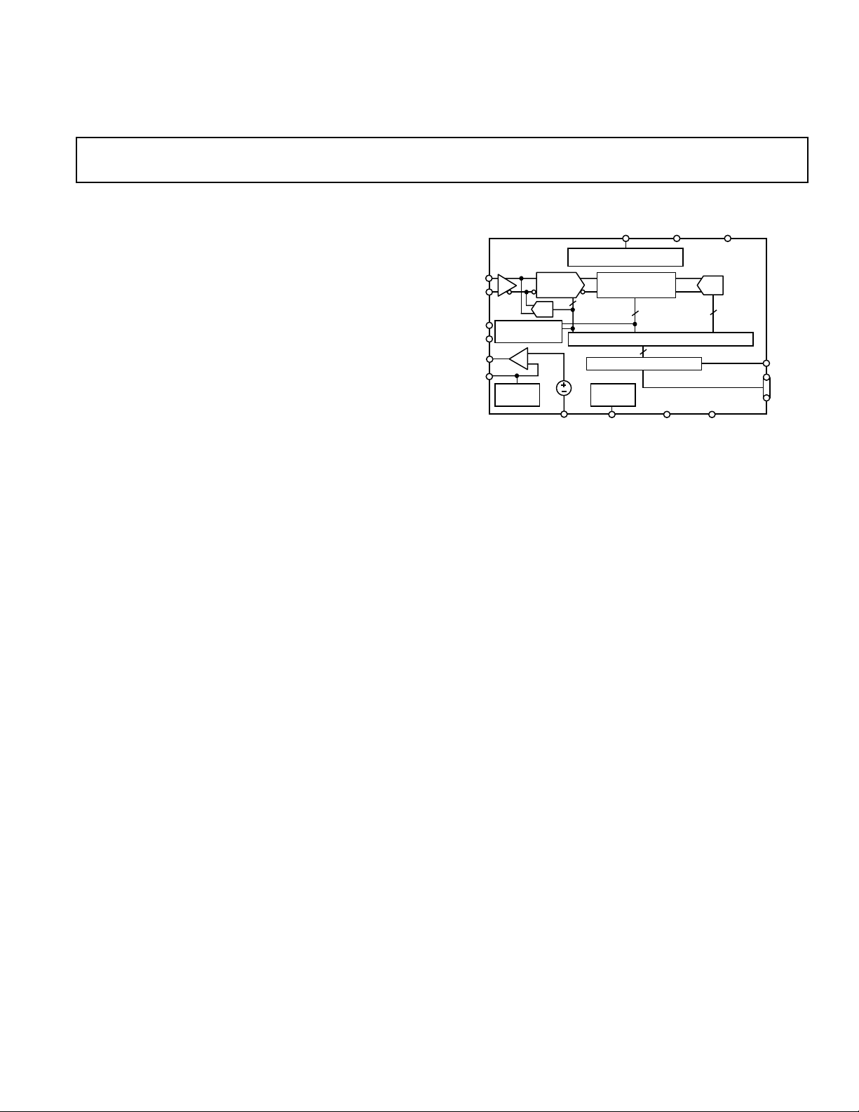
ADC Converter
AD9226
FUNCTIONAL BLOCK DIAGRAM
A/D
AD9226
DRVSS
DRVDD
3
OTR
BIT 1
(MSB)
BIT 12
(LSB)
AVDD
16
12
AVSS
VINA
VINB
CAPT
CAPB
VREF
SENSE
SHA
CALIBRATION
SELECT
REF
MDAC1
A/D
ROM
1V
REFCOM
CLK
DUTY CYCLE STABILIZER
8-STAGE
1-1/2-BIT PIPELINE
4
CORRECTION LOGIC
OUTPUT BUFFERS
MODE
SELECT
MODE
The AD9226 has two important mode functions. One will set
the data format to binary or two’s complement. The second will
make the ADC immune to clock duty cycle variations.
PRODUCT HIGHLIGHTS
IF Sampling—The patented SHA input can be configured for
either single-ended or differential inputs. It will maintain outstanding AC performance up to input frequencies of 300 MHz.
Low Power—The AD9226 at 475 mW consumes a fraction of
the power presently available in existing, high-speed monolithic
solutions.
Out of Range (OTR)—The OTR output bit indicates when
the input signal is beyond the AD9226’s input range.
Single Supply—The AD9226 uses a single 5 V power supply
simplifying system power supply design. It also features a separate digital output driver supply line to accommodate 3 V and
5 V logic families.
Pin Compatibility—The AD9226 is similar to the AD9220,
AD9221, AD9223, AD9224, and AD9225 ADCs.
Clock Duty Cycle Stabilizer—Makes conversion immune to
varying clock pulsewidths.
REV. 0
Information furnished by Analog Devices is believed to be accurate and
reliable. However, no responsibility is assumed by Analog Devices for its
use, nor for any infringements of patents or other rights of third parties
which may result from its use. No license is granted by implication or
otherwise under any patent or patent rights of Analog Devices.
One Technology Way, P.O. Box 9106, Norwood, MA 02062-9106, U.S.A.
Tel: 781/329-4700 World Wide Web Site: http://www.analog.com
Fax: 781/326-8703 © Analog Devices, Inc., 2000
Page 2

AD9226–SPECIFICATIONS
(AVDD = 5 V, DRVDD = 3 V, f
DC SPECIFICATIONS
P
arameter Temp Test Level Min Typ Max Unit
RESOLUTION 12 Bits
ACCURACY
Integral Nonlinearity (INL) Full V ± 0.6 LSB
Differential Nonlinearity (DNL) Full V ± 0.6 LSB
No Missing Codes Guaranteed Full I 12 Bits
Zero Error Full V ± 0.3 % FSR
Gain Error 25°CI ± 2.0 % FSR
TEMPERATURE DRIFT
Zero Error Full V ± 2 ppm/°C
Gain Error
Gain Error
POWER SUPPLY REJECTION
AVDD (5 V ± 0.25 V) Full V ± 0.05 % FSR
INPUT REFERRED NOISE
VREF = 1.0 V Full V 0.5 LSB rms
VREF = 2.0 V Full V 0.25 LSB rms
ANALOG INPUT
Input Span (VREF = 1 V) Full V 1 V p-p
Input (VINA or VINB) Range Full IV 0 AVDD V
Input Capacitance Full V 7 pF
INTERNAL VOLTAGE REFERENCE
Output Voltage (1 V Mode) Full V 1.0 V
Output Voltage Tolerance (1 V Mode) 25°CI ± 15 mV
Output Voltage (2.0 V Mode) Full V 2.0 V
Output Voltage Tolerance (2.0 V Mode) 25°CI ± 29 mV
Output Current (Available for External Loads) Full V 1.0 mA
Load Regulation
REFERENCE INPUT RESISTANCE Full V 5 kΩ
POWER SUPPLIES
Supply Voltages
AVDD Full V 4.75 5 5.25 V (± 5% AVDD
DRVDD Full V 2.85 5.25 V (± 5% DRVDD
Supply Current
IAVDD
IDRVDD
POWER CONSUMPTION
NOTES
1
Includes internal voltage reference error.
2
Excludes internal voltage reference error.
3
Load regulation with 1 mA load current (in addition to that required by the AD9226).
4
AVDD = 5 V
5
DRVDD = 3 V
Specifications subject to change without notice.
1
2
(VREF = 2 V) Full V 2 V p-p
3
4
5
4, 5
noted.)
25°CI ± 1.6 LSB
25°CI ± 1.0 LSB
25°CI ± 1.4 % FSR
Full V ± 0.6 % FSR
Full V ± 26 ppm/°C
Full V ± 0.4 ppm/°C
25°CI ± 0.4 % FSR
Full V 0.7 mV
25°C I 1.5 mV
Full V 86 mA (2 V External VREF)
25°C I 90.5 mA (2 V External VREF)
Full V 14.6 mA (2 V External VREF)
25°C I 16.5 mA (2 V External VREF)
Full V 475
25°C I 500 mW (2 V External VREF)
= 65 MSPS, VREF = 2.0 V, Differential inputs, T
SAMPLE
MIN
to T
unless otherwise
MAX
Operating)
Operating)
–2–
REV. 0
Page 3
AD9226
DIGITAL SPECIFICATIONS
(AVDD = 5 V, DRVDD = 3 V, f
= 65 MSPS, VREF = 2.0 V, T
SAMPLE
MIN
to T
, unless otherwise noted.)
MAX
Parameters Temp Test Level Min Typ Max Unit
LOGIC INPUTS (Clock, DFS
Output Enable
1
)
1
, Duty Cycle1, and
High-Level Input Voltage Full IV 2.4 V
Low-Level Input Voltage Full IV 0.8 V
High-Level Input Current (V
Low-Level Input Current (V
Input Capacitance Full V 5 pF
Output Enable
1
= AVDD) Full IV –10 +10 µA
IN
= 0 V) Full IV –10 +10 µA
IN
Full IV V
DRVDD
2
05– .
DRVDD
2
05+ .
LOGIC OUTPUTS (With DRVDD = 5 V)
High-Level Output Voltage (I
High-Level Output Voltage (I
Low-Level Output Voltage (I
Low-Level Output Voltage (I
= 50 µA) Full IV 4.5 V
OH
= 0.5 mA) Full IV 2.4 V
OH
= 1.6 mA) Full IV 0.4 V
OL
= 50 µA) Full IV 0.1 V
OL
Output Capacitance 5pF
LOGIC OUTPUTS (With DRVDD = 3 V)
High-Level Output Voltage (I
High-Level Output Voltage (I
Low-Level Output Voltage (I
= 50 µA) Full IV 2.95 V
OH
= 0.5 mA) Full IV 2.80 V
OH
= 1.6 mA) Full IV 0.4 V
OL
Low-Level Output Voltage (IOL = 50 µA) Full IV 0.05 V
NOTES
1
LQFP package.
Specifications subject to change without notice.
(T
to T
SWITCHING SPECIFICATIONS
MIN
with AVDD = 5 V, DRVDD = 3 V, CL = 20 pF)
MAX
Parameters Temp Test Level Min Typ Max Unit
Max Conversion Rate Full VI 65 MHz
Clock Period
CLOCK Pulsewidth High
CLOCK Pulsewidth Low
1
2
2
Full V 15.38 ns
Full V 3 ns
Full V 3 ns
Output Delay Full V 3.5 7 ns
Pipeline Delay (Latency) Full V 7 Clock Cycles
Output Enable Delay
NOTES
1
The clock period may be extended to 10 µs without degradation in specified performance @ 25°C.
2
When MODE pin is tied to AVDD or grounded, the AD9226 SSOP is not affected by clock duty cycle.
3
LQFP package.
Specifications subject to change without notice.
3
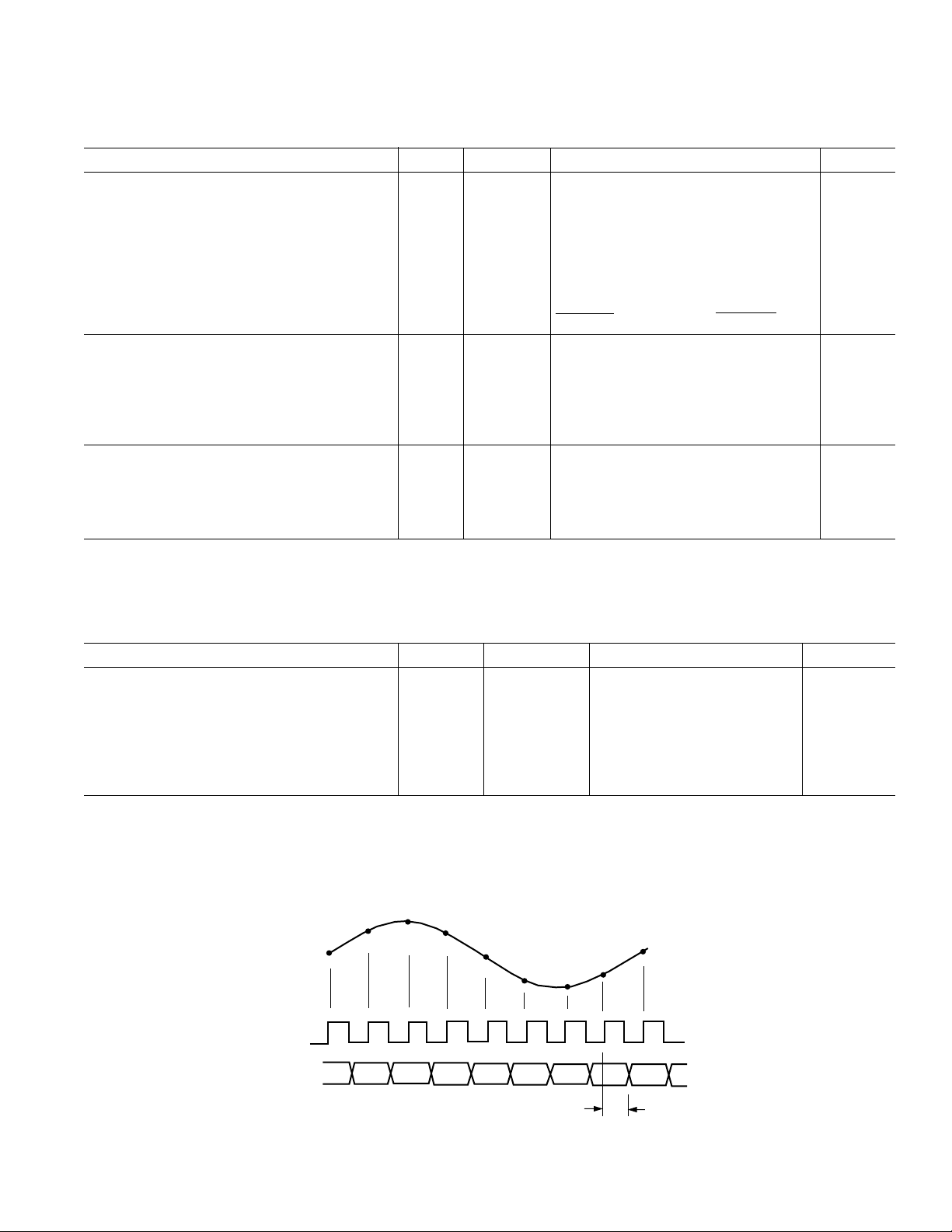
n+1
ANALOG
INPUT
CLOCK
DATA
n
n–8 n–7 n–6 n–5 n–4 n–3
OUT
Full V 15 ns
n+2
n+3
n+7
n–1
n+8
n
n+1
n+4
n+5
n+6
n–2
REV. 0
Figure 1. Timing Diagram
–3–
TOD = 7.0 MAX
3.5 MIN
Page 4

AD9226–SPECIFICATIONS
AC SPECIFICATIONS
(AVDD = 5 V, DRVDD = 3 V, f
= 65 MSPS, VREF = 2.0 V, T
SAMPLE
MIN
to T
, Differential Input unless otherwise noted.)
MAX
Parameter Temp Test Level Min Typ Max Unit
SIGNAL-TO-NOISE RATIO
fIN = 2.5 MHz Full V 68.9 dBc
25°C
= 15 MHz Full V 68.4 dBc
f
IN
25°C
f
= 31 MHz Full V 68 dBc
IN
= 60 MHz Full V 68 dBc
f
IN
fIN = 200 MHz
1
Full V 65 dBc
I 68 dBc
I 67.4 dBc
SIGNAL-TO-NOISE RATIO AND DISTORTION
fIN = 2.5 MHz Full V 68.8 dBc
25°C
= 15 MHz Full V 68.3 dBc
f
IN
25°C
= 31 MHz Full V 67 dBc
f
IN
= 60 MHz Full V 67 dBc
f
IN
fIN = 200 MHz
1
Full V 60 dBc
I 67.9 dBc
I 67.3 dBc
TOTAL HARMONIC DISTORTION
fIN = 2.5 MHz Full V –84 dBc
25°C
f
= 15 MHz Full V –82.3 dBc
IN
25°C
= 31 MHz Full V –68 dBc
f
IN
f
= 60 MHz Full V –68 dBc
IN
fIN = 200 MHz
1
Full V –61 dBc
I –77.0 dBc
I –76.0 dBc
SECOND AND THIRD HARMONIC DISTORTION
fIN = 2.5 MHz Full V –86.5 dBc
25°C
f
= 15 MHz Full V –86.7 dBc
IN
25°C
= 31 MHz Full V –83 dBc
f
IN
f
= 60 MHz Full V –82 dBc
IN
fIN = 200 MHz
1
Full V –75 dBc
I –78 dBc
I –76 dBc
SPURIOUS FREE DYNAMIC RANGE
fIN = 2.5 MHz Full V 86.4 dBc
25°C
f
= 15 MHz Full V 85.5 dBc
IN
25°C
= 31 MHz Full V 82 dBc
f
IN
f
= 60 MHz Full V 81 dBc
IN
fIN = 200 MHz
1
Full V 60 dBc
I 78 dBc
I 76 dBc
ANALOG INPUT BANDWIDTH 25°C V 750 MHz
NOTES
1
1.0 V Reference and Input Span
Specifications subject to change without notice.
–4–
REV. 0
Page 5
AD9226
WARNING!
ESD SENSITIVE DEVICE
EXPLANATION OF TEST LEVELS
Test Level
I. 100% production tested.
II. 100% production tested at 25°C and sample tested at
specified temperatures. AC testing done on sample basis.
III. Sample tested only.
IV. Parameter is guaranteed by design and characterization
testing.
V. Parameter is a typical value only.
VI. All devices are 100% production tested at 25°C; sample tested
at temperature extremes.
ABSOLUTE MAXIMUM RATINGS
1
With
Pin Name Respect to Min Max Unit
AVDD AVSS –0.3 +6.5 V
DRVDD DRVSS –0.3 +6.5 V
AVSS DRVSS –0.3 +0.3 V
AVDD DRVDD –6.5 +6.5 V
REFCOM AVSS –0.3 +0.3 V
CLK, MODE AVSS –0.3 AVDD + 0.3 V
Digital Outputs DRVSS –0.3 DRVDD + 0.3 V
VINA, VINB AVSS –0.3 AVDD + 0.3 V
VREF AVSS –0.3 AVDD
SENSE AVSS –0.3 AVDD
CAPB, CAPT AVSS –0.3 AVDD
2
OEB
CM LEVEL
2
VR
DRVSS –0.3 DRVDD + 0.3 V
2
AVSS –0.3 AVDD + 0.3 V
AVSS –0.3 AVDD + 0.3 V
+ 0.3 V
+ 0.3 V
+ 0.3 V
Junction Temperature 150 °C
Storage Temperature –65 +150 °C
Lead Temperature (10 sec) 300 °C
NOTES
1
Stresses above those listed under Absolute Maximum Ratings may cause perma-
nent damage to the device. This is a stress rating only; functional operation of the
device at these or any other conditions above those indicated in the operational
sections of this specification is not implied. Exposure to absolute maximum ratings
for extended periods may affect device reliability.
2
LQFP package.
THERMAL RESISTANCE
θJC SSOP . . . . . . . . . . . . . . . . . . . . . . . . . . . . . . . . . . . 23°C/W
θ
SSOP . . . . . . . . . . . . . . . . . . . . . . . . . . . . . . . . . . 63.3°C/W
JA
LQFP . . . . . . . . . . . . . . . . . . . . . . . . . . . . . . . . . . . 17°C/W
θ
JC
θ
LQFP . . . . . . . . . . . . . . . . . . . . . . . . . . . . . . . . . .76.2°C/W
JA
ORDERING GUIDE
Model Temperature Range Package Description Package Option
AD9226ARS –40°C to +85°C 28-Lead Shrink Small Outline (SSOP) RS-28
AD9226AST –40°C to +85°C 48-Lead Thin Plastic Quad Flatpack (LQFP) ST-48
AD9226-EB Evaluation Board (SSOP)
AD9226-LQFP-EB Evaluation Board (LQFP)
CAUTION
ESD (electrostatic discharge) sensitive device. Electrostatic charges as high as 4000 V readily
accumulate on the human body and test equipment and can discharge without detection. Although
the AD9226 features proprietary ESD protection circuitry, permanent damage may occur on
devices subjected to high-energy electrostatic discharges. Therefore, proper ESD precautions are
recommended to avoid performance degradation or loss of functionality.
REV. 0
–5–
Page 6
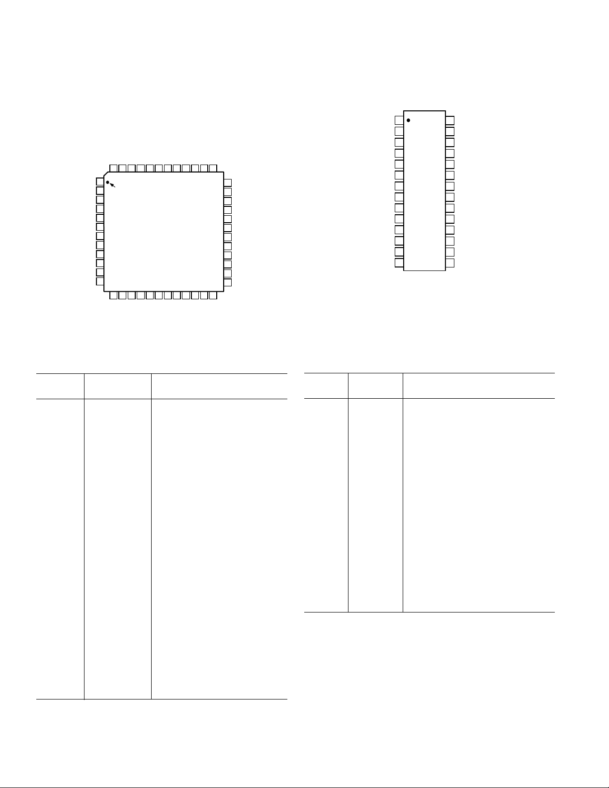
AD9226
AVSS
AVSS
AVDD
AVDD
NC
NC
CLK
NC
OEB
NC
NC
(LSB) BIT 12
NC = NO CONNECT
48-PIN FUNCTION DESCRIPTIONS
PIN CONNECTION
48-Lead LQFP
VR
VINB
VINA
CM LEVELNCMODE1
CAPT
AD9226
BIT 9
BIT 8
BIT 7
CAPT
BIT 6
48 47 46 45 44 39 38 3743 42 41 40
1
PIN 1
2
IDENTIFIER
3
4
5
6
7
8
9
10
11
12
13 14 15 16 17 18 19 20 21 22 23 24
BIT 11
DRVSS
DRVDD
TOP VIEW
(Not to Scale)
BIT 10
CAPB
CAPB
REF COM (AVSS)
BIT 5
DRVSS
DRVDD
VREF
BIT 4
36
SENSE
35
MODE2
34
AVDD
33
AVSS
32
AVSS
31
AVDD
30
DRVSS
29
DRVDD
28
OTR
BIT 1 (MSB)
27
BIT 2
26
BIT 3
25
PIN CONNECTION
28-Lead SSOP
CLK
(LSB) BIT 12
BIT 11
BIT 10
BIT 9
BIT 8
BIT 7
BIT 6
BIT 5
BIT 4
BIT 3
BIT 2
(MSB) BIT 1
OTR
1
2
3
4
5
6
AD9226
7
TOP VIEW
(Not to Scale)
8
9
10
11
12
13
14
28
DRVDD
27
DRVSS
26
AVDD
25
AVSS
24
VINB
23
VINA
22
MODE
21
CAPT
20
CAPB
19
REFCOM (AVSS)
18
VREF
17
SENSE
16
AVSS
15
AVDD
28-PIN FUNCTION DESCRIPTIONS
Pin
Number Name Description
1, 2, 32, 33 AVSS Analog Ground
3, 4, 31, 34 AVDD 5 V Analog Supply
5, 6, 8, 10, NC No Connect
11, 44
7 CLK Clock Input Pin
9 OEB Output Enable (Active Low)
12 BIT 12 Least Significant Data Bit (LSB)
13 BIT 11 Data Output Bit
14, 22, 30 DRVSS Digital Output Driver Ground
15, 23, 29 DRVDD 3 V to 5 V Digital Output
Driver Supply
16–21, BITS 10–5, Data Output Bits
24–26 BITS 4–2
27 BIT 1 Most Significant Data Bit (MSB)
28 OTR Out of Range
35 MODE2 Data Format Select
36 SENSE Reference Select
37 VREF Reference In/Out
38 REFCOM Reference Common
(AVSS)
39, 40 CAPB Noise Reduction Pin
41, 42 CAPT Noise Reduction Pin
43 MODE1 Clock Stabilizer
45 CM LEVEL Midsupply Reference
46 VINA Analog Input Pin (+)
47 VINB Analog Input Pin (–)
48 VR Noise Reduction Pin
Pin
Number Name Description
1 CLK Clock Input Pin
2 BIT 12 Least Significant Data Bit (LSB)
3–12 BITS 11–2 Data Output Bits
13 BIT 1 Most Significant Data Bit (MSB)
14 OTR Out of Range
15, 26 AVDD 5 V Analog Supply
16, 25 AVSS Analog Ground
17 SENSE Reference Select
18 VREF Input Span Select (Reference I/O)
19 REFCOM Reference Common
(AVSS)
20 CAPB Noise Reduction Pin
21 CAPT Noise Reduction Pin
22 MODE Data Format Select /Clock Stabilizer
23 VINA Analog Input Pin (+)
24 VINB Analog Input Pin (–)
27 DRVSS Digital Output Driver Ground
28 DRVDD 3 V to 5 V Digital Output
Driver Supply
–6–
REV. 0
Page 7

AD9226
DEFINITIONS OF SPECIFICATIONS
INTEGRAL NONLINEARITY (INL)
INL refers to the deviation of each individual code from a line
drawn from “negative full scale” through “positive full scale.”
The point used as “negative full scale” occurs 1/2 LSB before
the first code transition. “Positive full scale” is defined as a level
1 1/2 LSB beyond the last code transition. The deviation is
measured from the middle of each particular code to the true
straight line.
DIFFERENTIAL NONLINEARITY (DNL, NO MISSING
CODES)
An ideal ADC exhibits code transitions that are exactly 1 LSB
apart. DNL is the deviation from this ideal value. Guaranteed
no missing codes to 12-bit resolution indicates that all 4096
codes, respectively, must be present over all operating ranges.
ZERO ERROR
The major carry transition should occur for an analog value
1/2 LSB below VINA = VINB. Zero error is defined as the
deviation of the actual transition from that point.
GAIN ERROR
The first code transition should occur at an analog value
1/2 LSB above negative full scale. The last transition should
occur at an analog value 1 1/2 LSB below the positive full scale.
Gain error is the deviation of the actual difference between first
and last code transitions and the ideal difference between first
and last code transitions.
TEMPERATURE DRIFT
The temperature drift for zero error and gain error specifies the
maximum change from the initial (25°C) value to the value at
T
or T
MIN
POWER SUPPLY REJECTION
MAX
.
The specification shows the maximum change in full scale from
the value with the supply at the minimum limit to the value with
the supply at its maximum limit.
EFFECTIVE NUMBER OF BITS (ENOB)
For a sine wave, SINAD can be expressed in terms of the number of bits. Using the following formula,
N = (SINAD – 1.76)/6.02
it is possible to obtain a measure of performance expressed as
N, the effective number of bits.
Thus, effective number of bits for a device for sine wave inputs
at a given input frequency can be calculated directly from its
measured SINAD.
TOTAL HARMONIC DISTORTION (THD)
THD is the ratio of the rms sum of the first six harmonic components to the rms value of the measured input signal and is
expressed as a percentage or in decibels.
SIGNAL-TO-NOISE RATIO (SNR)
SNR is the ratio of the rms value of the measured input signal to
the rms sum of all other spectral components below the Nyquist
frequency, excluding the first six harmonics and dc. The value
for SNR is expressed in decibels.
SPURIOUS FREE DYNAMIC RANGE (SFDR)
SFDR is the difference in dB between the rms amplitude of the
input signal and the peak spurious signal.
ENCODE PULSEWIDTH DUTY CYCLE
Pulsewidth high is the minimum amount of time that the clock
pulse should be left in the logic “1” state to achieve rated performance; pulsewidth low is the minimum time the clock pulse
should be left in the low state. At a given clock rate, these specs
define an acceptable clock duty cycle.
MINIMUM CONVERSION RATE
The clock rate at which the SNR of the lowest analog signal
frequency drops by no more than 3 dB below the guaranteed limit.
MAXIMUM CONVERSION RATE
The encode rate at which parametric testing is performed.
APERTURE JITTER
Aperture jitter is the variation in aperture delay for successive
samples and can be manifested as noise on the input to the ADC.
APERTURE DELAY
Aperture delay is a measure of the sample-and-hold amplifier
(SHA) performance and is measured from the rising edge of the
clock input to when the input signal is held for conversion.
SIGNAL-TO-NOISE AND DISTORTION (S/N+D, SINAD)
RATIO
S/N+D is the ratio of the rms value of the measured input
signal to the rms sum of all other spectral components below
the Nyquist frequency, including harmonics but excluding dc.
The value for S/N+D is expressed in decibels.
REV. 0
–7–
OUTPUT PROPAGATION DELAY
The delay between the clock logic threshold and the time when
all bits are within valid logic levels.
TWO TONE SFDR
The ratio of the rms value of either input tone to the rms value
of the peak spurious component. The peak spurious component
may or may not be an IMD product. May be reported in dBc
(i.e., degrades as signal levels are lowered) or in dBFS (always
related back to converter full scale).
Page 8
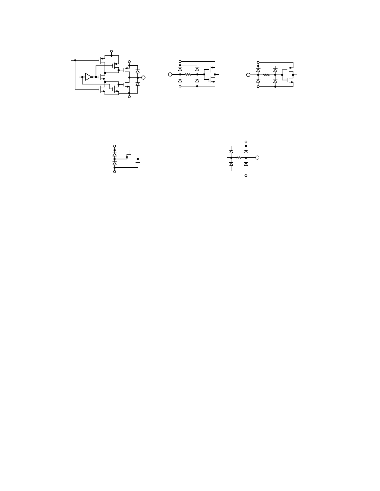
AD9226
DRVDD
DRVDD
DRVDD
AVDD
DRVSS
a. D0–D11, OTR
AVDD
AVSS
d. AIN e. CAPT, CAPB, MODE, SENSE, VREF
DRVSS
b. Three-State (OEB)
Figure 2. Equivalent Circuits
AVSS
c. CLK
AVDD
AVSS
–8–
REV. 0
Page 9
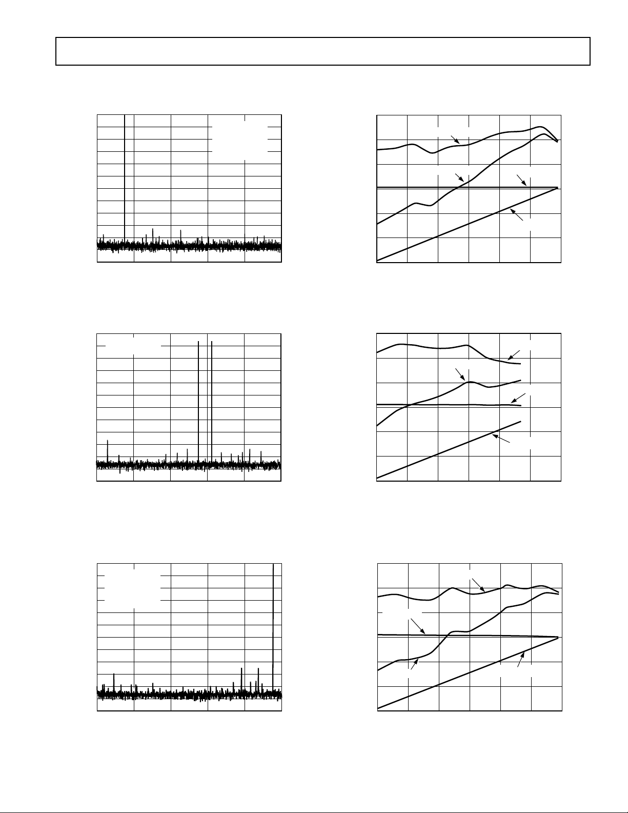
Typical Performance Characteristics–A
SNR – dBFS
SFDR – dBc
SNR – dBc
100
80
60
40
dBFS AND dBc
50
70
90
A
IN
– dBFS
–30
–25 –20
–15 –10
0
–5
SFDR – dBFS
D9226
(AVDD = 5.0 V, DRVDD = 3.0 V, f
V
= 2.0 V, unless otherwise noted.)
REF
0
–10
–20
–30
–40
–50
–60
dBFS
–70
–80
–90
–100
–110
–120
0
TPC 1. Single-Tone 8K FFT with fIN = 5 MHz
0
SNR = 70.4dBFS
–10
SFDR = 87.5dBFS
–20
–30
–40
–50
–60
dBFS
–70
–80
–90
–100
–110
–120
0
FREQUENCY – MHz
= 65 MSPS with CLK Stabilizer Enabled, TA = 25ⴗC, 2 V Differential Input Span, VCM = 2.5 V, AIN = –0.5 dBFS,
SAMPLE
100
FREQUENCY – MHz
SNR = 69.9dBc
SINAD = 69.8dBc
ENOB = 11.4BITS
THD = –86.4dBc
SFDR = 88.7dBc
90
80
70
dBFS AND dBc
60
50
32.56.5 13 19.5 26
40
–30
–25 –20
SFDR – dBFS
SFDR – dBc
–15 –10
– dBFS
A
IN
SNR – dBFS
SNR – dBc
TPC 4. Single-Tone SNR/SFDR vs. AIN with fIN = 5 MHz
32.56.5 13 19.5 26
–5
0
TPC 2. Dual-Tone 8K FFT with f
f
= 20 MHz (A
IN–2
0
–10
–20
–30
–40
–50
–60
dBFS
–70
–80
–90
–100
–110
–120
0 32.56.5 13 19.5 26
IN–1 = AIN–2
SNR = 69.5dBc
SINAD = 69.4dBc
ENOB = 11.3BITS
THD = –85dBc
SFDR = 87.6dBc
FREQUENCY – MHz
TPC 3. Single-Tone 8K FFT with fIN = 31 MHz
REV. 0
= –6.5 dBFS)
= 18 MHz and
IN–1
TPC 5. Dual-Tone SNR/SFDR vs. AIN with f
and f
= 20 MHz
IN–2
100
90
80
70
dBFS AND dBc
60
50
40
–30
SNR – dBFS
SFDR – dBc
–25 –20
SFDR – dBFS
–15 –10
– dBFS
A
IN
IN–1
SNR – dBc
–5
TPC 6. Single-Tone SNR/SFDR vs. AIN with fIN = 31 MHz
–9–
= 18 MHz
0
Page 10

AD9226
75
70
65
60
SINAD – dBc
55
50
45
1 1000
2V SPAN, DIFFERENTIAL
2V SPAN, SINGLE-ENDED
10
FREQUENCY – MHz
100
1V SPAN,
DIFFERENTIAL
1V SPAN,
SINGLE-ENDED
TPC 7. SINAD/ENOB vs. Frequency
–45
–50
–55
–60
–65
–70
THD – dBc
–75
–80
–85
–90
1 1000
2V SPAN, SINGLE-ENDED
10
FREQUENCY – MHz
100
1V SPAN,
SINGLE-ENDED
2V SPAN,
DIFFERENTIAL
1V SPAN,
DIFFERENTIAL
TPC 8. THD vs. Frequency
12.2
11.4
10.6
9.8
8.9
8.1
7.3
ENOB – Bits
71
70
69
68
67
66
SNR – dBc
65
64
63
62
61
1 1000
2V SPAN, SINGLE-ENDED
1V SPAN,
DIFFERENTIAL
1V SPAN,
SINGLE-ENDED
FREQUENCY – MHz
2V SPAN, DIFFERENTIAL
10010
TPC 10. SNR vs. Frequency
95
90
85
80
75
70
65
SFDR – dBc
60
55
50
45
1 1000
2V SPAN, SINGLE-ENDED
10
FREQUENCY – MHz
1V SPAN,
DIFFERENTIAL
2V SPAN,
DIFFERENTIAL
1V SPAN,
SINGLE-ENDED
100
TPC 11. SFDR vs. Frequency
72
–40ⴗC
70
68
SNR – dBc
66
64
62
1 1000
+25ⴗC
+85ⴗC
10
FREQUENCY – MHz
100
TPC 9. SNR vs. Temperature and Frequency
–10–
–70
–72
–74
–76
–78
–80
THD – dBc
–82
–84
–86
–88
–90
+25ⴗC
–40ⴗC
1
FREQUENCY – MHz
+85ⴗC
TPC 12. THD vs. Temperature and Frequency
10010
REV. 0
Page 11

AD9226
% POSITIVE DUTY CYCLE
30 45
SINAD/SFDR – dBc
35 50 55 70
45
50
55
60
65
70
75
80
85
90
40 60 65
SFDR – CLOCK STABILIZER ON
SINAD – CLOCK STABILIZER ON
SFDR – CLOCK STABILIZER OFF
SINAD – CLOCK STABILIZER OFF
105
95
85
75
HARMONICS – dBc
65
55
1 1000
3RD HARMONIC
2ND HARMONIC
10
FREQUENCY – MHz
4th HARMONIC
100
TPC 13. Harmonics vs. Frequency
100
95
fIN = 2MHz
90
SFDR – dBc
fIN = 12MHz
70.5
70.25
70
fIN = 12MHz
69.75
SINAD – dBc
69.5
69.25
69
10 20 30 40 50 7060
fIN = 2MHz
fIN = 20MHz
SAMPLE RATE – MSPS
TPC 16. SINAD vs. Sample Rate
REV. 0
85
fIN = 20MHz
80
10 20 30 40 50 7060
TPC 14. SFDR vs. Sample Rate
70.5
70.25
70
fIN = 12MHz
69.75
SINAD – dBc
69.5
fIN = 20MHz
69.25
69
10 20 30 40 50 7060
TPC 15. Typical INL
SAMPLE RATE – MSPS
fIN = 2MHz
SAMPLE RATE – MSPS
–11–
TPC 17. SINAD/SFDR vs. Duty Cycle @ fIN = 20 MHz
1
0.8
0.6
0.4
0.2
0
DNL – LSB
–0.2
–0.4
–0.6
–0.8
–1
0
500
1k
1500 2k 2500 3k 3500 4k
CODE
TPC 18. Typical DNL
Page 12

AD9226
AD9226–Typical IF Sampling Performance Characteristics
(AVDD = 5.0 V, DRVDD = 3.0 V, f
V
= 2.0 V, unless otherwise noted.)
REF
0
SNR = 70.2dBFS
–10
SFDR = 89dBFS
NOISE FLOOR = 145.33dBFS/Hz
–20
–30
–40
–50
–60
dBFS
–70
–80
–90
–100
–110
–120
4
024
8
= 65 MSPS with CLK Stabilizer Enabled, TA = 25ⴗC, 2 V Differential Input Span, VCM = 2.5 V, AIN = –6.5 dBFS,
SAMPLE
12 16
FREQUENCY – MHz
TPC 19. Dual-Tone 8K FFT with f
= 45.6 MHz
f
IN–2
0
–10
–20
–30
–40
–50
–60
dBFS
–70
–80
–90
–100
–110
–120
02441216
828
SNR = 68.5dBFS
SFDR = 75dBFS
NOISE FLOOR = 143.6dBFS/Hz
FREQUENCY – MHz
TPC 20. Dual-Tone 8K FFT with f
f
= 70.6 MHz
IN–2
20
= 44.2 MHz and
IN–1
20
= 69.2 MHz and
IN–1
28
95
90
85
80
SNR/SFDR – dBFS
75
70
65
32
–24
TPC 22. Dual-Tone SNR and SFDR with f
and f
32
= 45.6 MHz
IN–2
90
85
80
75
SNR/SFDR – dBFS
70
65
60
–24
SFDR – 2V SPAN
SNR/NOISE FLOOR – 2V SPAN
–21
SFDR – 1V SPAN
SNR/NOISE FLOOR – 2V SPAN
–18
SNR/NOISE FLOOR – 1V SPAN
–21
–18
–15 –12 –9
A
– dBFS
IN
SFDR – 2V SPAN
–15 –12 –9
A
– dBFS
IN
IN–1
TPC 23. Dual-Tone SNR and SFDR with f
and f
= 70.6 MHz
IN–2
170.1
165.1
160.1
155.1
150.1
145.1
140.1
–6
= 44.2 MHz
165.1
160.1
155.1
150.1
145.1
140.1
135.1
–6
= 69.2 MHz
IN–1
NOISE FLOOR – dBFS/Hz
NOISE FLOOR – dBFS/Hz
0
–10
–20
–30
–40
–50
–60
dBFS
–70
–80
–90
–100
–110
–120
4
024
8
SNR = 67.5dBFS
SFDR = 75dBFS
NOISE FLOOR = 142.6dBFS/Hz
12 16
FREQUENCY – MHz
TPC 21. Dual-Tone 8K FFT with f
f
= 140.7 MHz
IN–2
20
= 139.2 MHz and
IN–1
28
90
SFDR – 2V SPAN
85
80
75
SNR/SFDR – dBFS
70
SNR/NOISE FLOOR – 1V SPAN
65
60
32
–24
TPC 24. Dual-Tone SNR and SFDR with f
–12–
–12–
and f
= 140.7 MHz
IN–2
–21
SFDR – 1V SPAN
SNR/NOISE FLOOR – 2V SPAN
–18
–15 –12 –9
A
– dBFS
IN
IN–1
165.1
160.1
155.1
150.1
145.1
NOISE FLOOR – dBFS/Hz
140.1
135.1
–6
= 139.2 MHz
REV. 0
REV. 0
Page 13

AD9226
0
–10
–20
–30
–40
–50
–60
dBFS
–70
–80
–90
–100
–110
–120
0
51520
10 30
FREQUENCY – MHz
fIN = 190.82MHz
= 61.44MSPS
f
SAMPLE
25
TPC 25. Single-Tone 8K FFT at IF = 190 MHz–WCDMA
= 190.82 MHz, f
(f
IN
0
SNR = 65.1dBFS
–10
SFDR = 59dBFS
NOISE FLOOR = 140.2dBFS/Hz
–20
–30
–40
–50
–60
dBFS
–70
–80
–90
–100
–110
–120
4
024
TPC 26. Dual-Tone 8K FFT with f
= 240.7 MHz
f
IN–2
SAMPLE
8
12 16
FREQUENCY – MHz
= 61.44 MSPS)
20
= 239.1 MHz and
IN–1
32
28
–6
165.1
160.1
155.1
150.1
145.1
NOISE FLOOR – dBFS/Hz
140.1
135.1
90
85
80
75
SNR/SFDR – dBFS
70
65
60
–24
SFDR – 1V SPAN
SNR/NOISE FLOOR – 2V SPAN
SNR/NOISE FLOOR – 1V SPAN
–21
–18
–15 –12 –9
A
– dBFS
IN
SFDR – 2V SPAN
TPC 28. Single-Tone SNR and SFDR vs. AIN at IF = 190 MHz
–WCDMA (f
85
80
75
70
SNR/SFDR – dBFS
65
60
55
–24
= 190.8 MHz, f
IN–1
SFDR – 2V SPAN
SNR/NOISE FLOOR – 2V SPAN
SNR/NOISE FLOOR – 1V SPAN
–21
–18 –15 –12 –9 –6
A
IN
– dBFS
TPC 29. Dual-Tone SNR and SFDR with f
and f
= 240.7 MHz
IN–2
= 61.44 MSPS)
SAMPLE
SFDR – 1V SPAN
= 239.1 MHz
IN–1
160.1
155.1
150.1
145.1
140.1
NOISE FLOOR – dBFS/Hz
135.1
130.1
–35
–45
–55
–65
INPUT SPAN = 2V p–p
CMRR – dBc
–75
–85
–95
1
INPUT SPAN = 1V p–p
10
FREQUENCY – MHz
TPC 27. CMRR vs. Frequency (A
CML = 2.5 V)
REV. 0
100
= –0 dBFS and
IN
1000
–13–
Page 14

AD9226
THEORY OF OPERATION
The AD9226 is a high-performance, single-supply 12-bit ADC.
The analog input of the AD9226 is very flexible allowing for both
single-ended or differential inputs of varying amplitudes that can
be ac- or dc-coupled.
It utilizes a nine-stage pipeline architecture with a wideband,
sample-and-hold amplifier (SHA) implemented on a costeffective CMOS process. A patented structure is used in the
SHA to greatly improve high frequency SFDR/distortion. This
also improves performance in IF undersampling applications.
Each stage of the pipeline, excluding the last stage, consists of a
low resolution flash ADC connected to a switched capacitor
DAC and interstage residue amplifier (MDAC). The residue
amplifier amplifies the difference between the reconstructed DAC
output and the flash input for the next stage in the pipeline. One
bit of redundancy is used in each of the stages to facilitate digital
correction of flash errors. The last stage simply consists of a
flash ADC.
Factory calibration ensures high linearity and low distortion.
ANALOG INPUT OPERATION
Figure 3 shows the equivalent analog input of the AD9226 which
consists of a 750 MHz differential SHA. The differential input
structure of the SHA is highly flexible, allowing the device to be
easily configured for either a differential or single-ended input.
The analog inputs, VINA and VINB, are interchangeable with
the exception that reversing the inputs to the VINA and VINB
pins results in a data inversion (complementing the output word).
The optimum noise and dc linearity performance for either
differential or single-ended inputs is achieved with the largest input
signal voltage span (i.e., 2 V input span) and matched input
impedance for VINA and VINB. Only a slight degradation in
dc linearity performance exists between the 2 V and 1 V input
spans.
High frequency inputs may find the 1 V span better suited to
achieve superior SFDR performance. (See Typical Performance Characteristics.)
The ADC samples the analog input on the rising edge of the clock
input. During the clock low time (between the falling edge and
rising edge of the clock), the input SHA is in the sample mode;
during the clock high time it is in hold. System disturbances just
prior to the rising edge of the clock and/or excessive clock jitter
on the rising edge may cause the input SHA to acquire the wrong
value and should be minimized.
When the ADC is driven by an op amp and a capacitive load is
switched onto the output of the op amp, the output will momentarily drop due to its effective output impedance. As the output
recovers, ringing may occur. To remedy the situation, a series
resistor can be inserted between the op amp and the SHA
input as shown in Figure 4. A shunt capacitance also acts like
a charge reservoir, sinking or sourcing the additional charge
required by the hold capacitor, C
, further reducing current
H
transients seen at the op amp’s output.
The optimum size of this resistor is dependent on several factors,
including the ADC sampling rate, the selected op amp, and the
particular application. In most applications, a 30 Ω to 100 Ω
resistor is sufficient.
For noise-sensitive applications, the very high bandwidth of the
AD9226 may be detrimental and the addition of a series resistor
and/or shunt capacitor can help limit the wideband noise at the
ADC’s input by forming a low-pass filter. The source impedance driving VINA and VINB should be matched. Failure to
provide matching will result in degradation of the AD9226’s
SNR, THD, and SFDR.
C
H
Q
S2
Q
S2
C
H
VINA
VINB
C
PIN
Q
S1
C
PAR
Q
S1
C
PIN
C
PAR
C
S
Q
C
H1
S
Figure 3. Equivalent Input Circuit
V
CC
V
EE
10F
R
33⍀
S
0.1F
R
33⍀
AD9226
VINA
15pF
S
VINB
VREF
SENSE
REFCOM
Figure 4. Series Resistor Isolates Switched-Capacitor
SHA Input from Op Amp; Matching Resistors Improve
SNR Performance
OVERVIEW OF INPUT AND REFERENCE
CONNECTIONS
The overall input span of the AD9226 is equal to the potential
at the VREF pin. The VREF potential may be obtained from
the internal AD9226 reference or an external source (see
Reference Operation section).
In differential applications, the center point of the span is
obtained by the common-mode level of the signals. In singleended applications, the center point is the dc potential applied
to one input pin while the signal is applied to the opposite input
pin. Figures 5a–5f show various system configurations.
DRIVING THE ANALOG INPUTS
The AD9226 has a very flexible input structure allowing it to
interface with single-ended or differential input interface circuitry.
The optimum mode of operation, analog input range, and associated interface circuitry will be determined by the particular
applications performance requirements as well as power supply
options.
DIFFERENTIAL DRIVER CIRCUITS
Differential operation requires that VINA and VINB be simultaneously driven with two equal signals that are 180ⴗ out of phase
with each other.
Differential modes of operation (ac- or dc-coupled input) provide
the best THD and SFDR performance over a wide frequency
range. They should be considered for the most demanding
spectral-based applications (e.g., direct IF conversion to digital).
–14–
REV. 0
Page 15

AD9226
10F
VINA
VREF
AD9226
VINB
2.0V
SENSE
0.1F
10F0.1F
0.1F
15pF
2.75V
33⍀
33⍀
1V
0.1F
49.9⍀
2.75V
2.25V
2.5V
2.5V
CAPT
CAPB
0.1F
2.5V
AVDD
10k⍀10k⍀
1.5V
0.5V
10F
33⍀
15pF
33⍀
1V
0.1F
AD9226
VINA
VINB
VREF
SENSE
REFCOM
0.1F
CAPT
10F0.1F
CAPB
0.1F
Figure 5a. 1 V Single-Ended Input, Common-Mode
Voltage = 1 V
1.25V
VINA
VINB
VREF
SENSE
AD9226
0.1F
CAPT
10F0.1F
CAPB
0.1F
0.75V
1.25V
0.75V
49.9⍀
33⍀
10F
33⍀
15pF
1V
0.1F
Figure 5b. 1 V Differential Input, Common-Mode
Voltage = 1 V
2.5V
3.0V
2.5V
2.0V
3.0V
2.5V
2.0V
49.9⍀
33⍀
33⍀
10F
0.1F
15pF
0.1F
CMLEVEL
AD9226
(LQFP)
VINA
VINB
2V
VREF
SENSE
0.1F
CAPT
10F0.1F
CAPB
0.1F
Figure 5e. 2 V Differential Input, Common-Mode
Voltage = 2.5 V
2.5V
VINA
VINB
VREF
SENSE
AD9226
0.1F
CAPT
CAPB
2.5V
1.5V
1.5V
49.9⍀
33⍀
10F
33⍀
15pF
2V
0.1F
Figure 5c. 2 V Differential Input, Common-Mode
Voltage = 2 V
3.0V
AD9226
VINA
VINB
VREF
SENSE
REFCOM
0.1F
CAPT
CAPB
1.0V
10F
Figure 5d. 2 V Single-Ended Input, Common-Mode
Voltage = 2 V
REV. 0
33⍀
15pF
33⍀
2V
0.1F
10F0.1F
0.1F
10F0.1F
0.1F
Figure 5f. 1 V Differential Input, Common-Mode
Voltage = 2.5 V (Recommended for IF Undersampling)
The differential input characterization for this data sheet was
performed using the configuration shown in Figure 7.
Since not all applications have a signal preconditioned for
differential operation, there is often a need to perform a singleended-to-differential conversion. In systems that do not need to
be dc-coupled, an RF transformer with a center tap is the best
method to generate differential inputs for the AD9226. It provides all the benefits of operating the ADC in the differential
mode without contributing additional noise or distortion. An RF
transformer also has the added benefit of providing electrical
isolation between the signal source and the ADC. An improvement
in THD and SFDR performance can be realized by operating
the AD9226 in the differential mode. The performance enhancement between the differential and single-ended mode is most
noteworthy as the input frequency approaches and goes beyond
the Nyquist frequency (i.e., f
> FS /2).
IN
The circuit shown in Figure 6a is an ideal method of applying
a differential dc drive to the AD9226. It uses an AD8138 to
derive a differential signal from a single-ended one. Figure 6b
illustrates its performance.
Figure 7 presents the schematic of the suggested transformer
circuit. The circuit uses a Minicircuits RF transformer, model
T1-1T, which has an impedance ratio of four (turns ratio of 2).
The schematic assumes that the signal source has a 50 Ω source
impedance. The center tap of the transformer provides a convenient means of level-shifting the input signal to a desired
common-mode voltage. In Figure 7 the transformer centertap
is connected to a resistor divider at the midsupply voltage.
–15–
Page 16

AD9226
1V p-p
4.7F
1k⍀
450⍀
49⍀
499⍀
0.1F
1k⍀
499⍀
AD8138
499⍀
49⍀
15pF
49⍀
VIN A
AD9226
VIN B
CAPT
CAPB
0.1F
0.1F
10F
0.1F
Figure 6a. Direct-Coupled Drive Circuit with AD8138
Differential Op Amp
0
–20
–40
–60
dBc
–80
–100
–120
048121620242832
MHz
SNR = 66.9dBc
SFDR = 70.0dBc
Figure 6b. FS = 65 MSPS, fIN = 30 MHz, Input Span = 1 V p-p
The same midsupply potential may be obtained from the
CMLEVEL pin of the AD9226 in the LQFP package.
Referring to Figure 7, a series resistor, R
, is inserted between the
S
AD9226 and the secondary of the transformer. The value of
33 ohm was selected to specifically optimize both the THD and
SNR performance of the ADC. R
and the internal capacitance
S
help provide a low-pass filter to block high-frequency noise.
Transformers with other turns ratios may also be selected to
optimize the performance of a given application. For example, a
given input signal source or amplifier may realize an improvement in distortion performance at reduced output power levels
and signal swings. By selecting a transformer with a higher
impedance ratio (e.g., Minicircuits T16-6T with a 1:16 impedance ratio), the signal level is effectively “stepped up” thus
further reducing the driving requirements of signal source.
AVDD
49.9⍀
MINICIRCUITS
T1-1T
0.1F
R
33⍀
S
R
33⍀
1k⍀
VINA
AD9226
1k⍀
S
15pF
VINB
0.1F
CAPT
10F0.1F
CAPB
0.1F
Figure 7. Transformer-Coupled Input
SINGLE-ENDED DRIVER CIRCUITS
The AD9226 can be configured for single-ended operation using
dc- or ac-coupling. In either case, the input of the ADC must be
driven from an operational amplifier that will not degrade the
ADC’s performance. Because the ADC operates from a single
supply, it will be necessary to level-shift ground-based bipolar
signals to comply with its input requirements. Both dc- and
ac-coupling provide this necessary function, but each method
results in different interface issues which may influence the
system design and performance.
Single-ended operation requires that VINA be ac- or dc-coupled
to the input signal source, while VINB of the AD9226 be biased
to the appropriate voltage corresponding to the middle of the input
span. The single-ended specifications for the AD9226 are characterized using Figure 9a circuitry with input spans of 1 V and
2 V. The common-mode level is 2.5 V.
If the analog inputs exceed the supply limits, internal parasitic
diodes will turn on. This will result in transient currents within
the device. Figure 8 shows a simple means of clamping an input.
It uses a series resistor and two diodes. An optional capacitor is
shown for ac-coupled applications. A larger series resistor can
be used to limit the fault current through D1 and D2. This
can cause a degradation in overall performance. A similar
clamping circuit can also be used for each input if a differential input signal is being applied. A better method to ensure
the input is not overdriven is to use amplifiers powered by a single
5 V supply such as the AD8138.
V
CC
V
EE
OPTIONAL
AC-COUPLING
CAPACITOR
R
30⍀
AVDD
S1
D2
D1
R
20⍀
S2
AD9226
Figure 8. Simple Clamping Circuit
AC-COUPLING AND INTERFACE ISSUES
For applications where ac-coupling is appropriate, the op amp
output can be easily level-shifted by means of a coupling
capacitor. This has the advantage of allowing the op amp’s common-mode level to be symmetrically biased to its midsupply
level (i.e., (AVDD/2). Op amps that operate symmetrically with
respect to their power supplies typically provide the best ac
performance as well as greatest input/output span. Various highspeed performance amplifiers that are restricted to +5 V/–5 V
operation and/or specified for 5 V single-supply operation can be
easily configured for the 2 V or 1 V input span of the AD9226.
Simple AC Interface
Figure 9a shows a typical example of an ac-coupled, singleended configuration of the SSOP package. The bias voltage
shifts the bipolar, ground-referenced input signal to approximately AVDD/2. The capacitors, C1 and C2, are 0.1 µF ceramic
and 10 µF tantalum capacitors in parallel to achieve a low
cutoff frequency while maintaining a low impedance over a
wide frequency range. The combination of the capacitor and the
resistor form a high-pass network with a high-pass –3 dB frequency determined by the equation,
= 1/(2 × π × R × (C1 + C2))
f
–3 dB
–16–
REV. 0
Page 17

AD9226
The low-impedance VREF output can be used to provide dc
bias levels to the fixed VINB pin and the signal on VINA. Figure 9b shows the VREF configured for 2.0 V, thus the input
range of the ADC is 1.0 V to 3.0 V. Other input ranges could
be selected by changing VREF.
When the inputs are biased from the reference (Figure 9b),
there may be a slight degeneration of dynamic performance. A
midsupply output level is available at the CM LEVEL pin of the
LQFP package.
+1V
0V
–1V
V
IN
0.1F
+5V
–5V
10F
C1
10F
C2
0.1F
3.5
2.5
1.5
VV
RR
15pF
R
R
R
S
VINA
AD9226
R
S
VINB
VREF
10F
0.1F
CAPT
10F0.1F
CAPB
0.1F
0.1F
Figure 9a. AC-Coupled Input Configuration
0.1F
V
IN
10F
10F
R
S
1k⍀
1k⍀
R
S
0.1F
15pF
VINA
VINB
AD9226
0.1F
CAPT
10F0.1F
CAPB
0.1F
VREF
0.1F10F
Figure 9b. Alternate AC-Coupled Input Configuration
–84
–83
–82
–81
–80
dBc
–79
–78
–77
–76
0
0.5 1.0 1.5 2.0 2.5 3.0 3.5 4.0 4.5 5.0
volts
Figure 10. THD vs. Common-Mode Voltage
(2 V Differential Input Span, f
= 10 MHz)
IN
Figure 10 illustrates the relation between common-mode voltage
and THD. Note that optimal performance occurs when the
reference voltage is set to 2.0 V (input span = 2.0 V).
DC-COUPLING AND INTERFACE ISSUES
Many applications require the analog input signal to be dc-coupled
to the AD9226. An operational amplifier can be configured to
rescale and level-shift the input signal to make it compatible
with the selected input range of the ADC.
The selected input range of the AD9226 should be considered
with the headroom requirements of the particular op amp to
prevent clipping of the signal. Many of the new high-performance
op amps are specified for only ±5 V operation and have limited
input/output swing capabilities. Also, since the output of a dual
supply amplifier can swing below absolute minimum (–0.3 V),
clamping its output should be considered in some applications
(see Figure 8). When single-ended, dc-coupling is needed, the
use of the AD8138 in a differential configuration (Figure 9a) is
highly recommended.
Simple Op Amp Buffer
In the simplest case, the input signal to the AD9226 will already
be biased at levels in accordance with the selected input range. It
is necessary to provide an adequately low source impedance for
the VINA and VINB analog pins of the ADC.
REFERENCE OPERATION
The AD9226 contains an on-board bandgap reference that
provides a pin-strappable option to generate either a 1 V or
2 V output. With the addition of two external resistors, the user
can generate reference voltages between 1 V and 2 V. See
Figures 5a-5f for a summary of the pin-strapping options for the
AD9226 reference configurations. Another alternative is to use
an external reference for designs requiring enhanced accuracy
and/or drift performance described later in this section.
Figure 11a shows a simplified model of the internal voltage reference of the AD9226. A reference amplifier buffers a 1 V fixed
reference. The output from the reference amplifier, A1, appears
on the VREF pin. The voltage on the VREF pin determines
the full-scale input span of the ADC. This input span equals,
Full-Scale Input Span = VREF
The voltage appearing at the VREF pin, and the state of the
internal reference amplifier, A1, are determined by the voltage
appearing at the SENSE pin. The logic circuitry contains comparators that monitor the voltage at the SENSE pin. If the
SENSE pin is tied to AVSS, the switch is connected to the
internal resistor network thus providing a VREF of 2.0 V. If the
SENSE pin is tied to the VREF pin via a short or resistor, the
switch will connect to the SENSE pin. This connection will provide a VREF of 1.0 V. An external resistor network will provide
an alternative VREF between 1.0 V and 2.0 V (see Figure 12).
Another comparator controls internal circuitry that will disable
the reference amplifier if the SENSE pin is tied to AVDD.
Disabling the reference amplifier allows the VREF pin to be
driven by an external voltage reference.
REV. 0
–17–
Page 18

AD9226
AD9226
TO
A/D
CAPT
A2
2.5V
CAPB
VREF
SENSE
REFCOM
1V
DISABLE
A1
LOGIC
A1
Figure 11a. Equivalent Reference Circuit
0.1F
CAPT
VREF
0.1F10F
AD9226
CAPB
0.1F
10F
0.1F
Figure 11b. CAPT and CAPB DC-Coupling
The actual reference voltages used by the internal circuitry of the
AD9226 appear on the CAPT and CAPB pins. The voltages
on these pins are symmetrical about the analog supply. For
proper operation when using an internal or external reference, it
is necessary to add a capacitor network to decouple these pins.
Figure 11b shows the recommended decoupling network. The
turn-on time of the reference voltage appearing between CAPT
and CAPB is approximately 10 ms and should be evaluated in
any power-down mode of operation.
USING THE INTERNAL REFERENCE
The AD9226 can be easily configured for either a 1 V p-p input
span or 2 V p-p input span by setting the internal reference.
Other input spans can be realized with two external gainsetting resistors as shown in Figure 12 of this data sheet, or
using an external reference.
Pin Programmable Reference
By shorting the VREF pin directly to the SENSE pin, the internal reference amplifier is placed in a unity-gain mode and the
resultant VREF output is 1 V. By shorting the SENSE pin
directly to the REFCOM pin, the internal reference amplifier is
configured for a gain of 2.0 and the resultant VREF output is
2.0 V. The VREF pin should be bypassed to the REFCOM pin
with a 10 µF tantalum capacitor in parallel with a low-inductance
0.1 µF ceramic capacitor as shown in Figure 11b.
Resistor Programmable Reference
Figure 12 shows an example of how to generate a reference
voltage other than 1.0 V or 2.0 V with the addition of two external resistors. Use the equation,
VREF = 1 V × (1 + R1/R2)
to determine appropriate values for R1 and R2. These resistors
should be in the 2 kΩ to 10 kΩ range. For the example shown,
R1 equals 2.5 kΩ and R2 equals 5 kΩ. From the equation above,
the resultant reference voltage on the VREF pin is 1.5 V. This
–18–
sets the input span to be 1.5 V p-p. The midscale voltage can
also be set to VREF by connecting VINB to VREF. Alternatively, the midscale voltage can be set to 2.5 V by connecting
VINB to a low-impedance 2.5 V source as shown in Figure 12.
10F
3.25V
1.75V
2.5V
0.1F
33⍀
33⍀
R1
2.5k⍀
R2
5k⍀
15pF
1.5V
0.1F
C1
AD9226
VINA
VINB
VREF
SENSE
REFCOM
0.1F
CAPT
10F0.1F
CAPB
0.1F
Figure 12. Resistor Programmable Reference (1.5 V p-p
Input Span, Differential Input V
= 2.5 V)
CM
USING AN EXTERNAL REFERENCE
The AD9226 contains an internal reference buffer, A2 (see
Figure 11b), that simplifies the drive requirements of an external
reference. The external reference must be able to drive about
5kΩ (±20%) load. Note that the bandwidth of the reference
buffer is deliberately left small to minimize the reference noise
contribution. As a result, it is not possible to rapidly change the
reference voltage in this mode.
Figure 13 shows an example of an external reference driving
both VINB and VREF. In this case, both the common-mode
voltage and input span are directly dependent on the value of
VREF. Both the input span and the center of the input span are
equal to the external VREF. Thus the valid input range extends
from (VREF + VREF/2) to (VREF – VREF/2). For example,
if the REF191, a 2.048 V external reference, is selected, the
input span extends to 2.048 V. In this case, 1 LSB of the AD9226
corresponds to 0.5 mV. It is essential that a minimum of a 10 µF
capacitor, in parallel with a 0.1 µF low-inductance ceramic
capacitor, decouple the reference output to ground.
To use an external reference, the SENSE pin must be connected
to AVDD. This connection will disable the internal reference.
VINA+VREF/2
VINB–VREF/2
5V
0.1F
VREF
10F
33⍀
15pF
33⍀
0.1F
5V
AD9226
VINA
VINB
VREF
SENSE
0.1F
CAPT
10F0.1F
CAPB
0.1F
Figure 13. Using an External Reference
MODE CONTROLS
Clock Stabilizer
The clock stabilizer is a circuit that desensitizes the ADC from
clock duty cycle variations. The AD9226 eases system clock
constraints by incorporating a circuit that restores the internal duty
cycle to 50%, independent of the input duty cycle. Low jitter on
the rising edge (sampling edge) of the clock is preserved while
the noncritical falling edge is generated on-chip.
It may be desirable to disable the clock stabilizer, and may be
necessary when the clock frequency speed is varied or completely
REV. 0
Page 19

AD9226
stopped. Once the clock frequency is changed, over 100 clock
cycles may be required for the clock stabilizer to settle to a different speed. When the stabilizer is disabled, the internal switching
will be directly affected by the clock state. If the external clock is
high, the SHA will be in hold. If the clock pulse is low, the SHA
will be in track. TPC 16 shows the benefits of using the clock
stabilizer. See Tables I and III.
Data Format Select (DFS)
The AD9226 may be set for binary or two’s complement data
output formats. See Tables I and II.
SSOP Package
The SSOP mode control (Pin 22) has two functions. It enables/
disables the clock stabilizer and determines the output data format.
The exact functions of the mode pin are outlined in Table I.
Table I. Mode Select (SSOP)
Mode DFS Clock Duty Cycle Shaping
DNC Binary Clock Stabilizer Disabled
AVDD Binary Clock Stabilizer Enabled
GND Two’s Complement Clock Stabilizer Enabled
10 kΩ Two’s Complement Clock Stabilizer Disabled
Resistor To GND
LQFP Package
Pin 35 of the LQFP package determines the output data format
(DFS). If it is connected to AVSS, the output word will be straight
binary. If it is connected to AVDD, the output data format will
be two’s complement. See Table II.
Pin 43 of the LQFP package controls the clock stabilizer function
of the AD9226. If the pin is connected to AVDD, both clock
edges will be used in the conversion architecture. When Pin 43
is connected to AVSS, the internal duty cycle will be determined
by the clock stabilizer function within the ADC. See Table III.
Table II. DFS Pin Controls
DFS Function Pin 35 Connection
Straight Binary AVDD
Two’s Complement AVSS
Table IV. Output Data Format
Two’s
Binary Complement
Input (V) Condition (V) Output Mode Mode OTR
VINA–VINB < – VREF 0000 0000 0000 1000 0000 0000 1
VINA–VINB = – VREF 0000 0000 0000 1000 0000 0000 0
VINA–VINB = 0 1000 0000 0000 0000 0000 0000 0
VINA–VINB = + VREF – 1 LSB 1111 1111 1111 0111 1111 1111 0
VINA–VINB ≥ + VREF 1111 1111 1111 0111 1111 1111 1
Out of Range (OTR)
An out-of-range condition exists when the analog input voltage
is beyond the input range of the converter. OTR is a digital
output that is updated along with the data output corresponding
to the particular sampled analog input voltage. Hence, OTR has
the same pipeline delay (latency) as the digital data. It is LOW
when the analog input voltage is within the analog input range.
It is HIGH when the analog input voltage exceeds the input
range as shown in Figure 14. OTR will remain HIGH until the
analog input returns within the input range and another conversion
is completed. By logical ANDing OTR with the MSB and its
complement, overrange high or underrange low conditions can be
detected. Table V is a truth table for the over/underrange
circuit in Figure 15, which uses NAND gates. Systems requiring
programmable gain conditioning of the AD9226 input signal
can immediately detect an out-of-range condition, thus eliminating gain selection iterations. Also, OTR can be used for
digital offset and gain calibration.
Table V. Out-of-Range Truth Table
OTR MSB Analog Input Is
0 0 In Range
0 1 In Range
1 0 Underrange
1 1 Overrange
OTR DATA OUTPUTS
1111 1111 1111
1
1111 1111 1111
0
1111 1111 1110
0
OTR
–FS +1/2 LSB
+FS – 1 1/2 LSB
Table III. Clock Stabilizer Pin
Clock Restore Function Pin 43 Connection
Clock Stabilizer Enabled AVDD
Clock Stabilizer Disabled AVSS
DIGITAL INPUTS AND OUTPUTS
Digital Outputs
Table IV details the relationship among the ADC input, OTR, and
straight binary output.
REV. 0
0000 0000 0001
0
0000 0000 0000
0
0000 0000 0000
1
–FS
+FS
+FS – 1/2 LSB–FS – 1/2 LSB
Figure 14. OTR Relation to Input Voltage and Output Data
MSB
OTR
MSB
OVER = 1
UNDER = 1
Figure 15. Overrange or Underrange Logic
–19–
Page 20

AD9226
Digital Output Driver Considerations
The AD9226 output drivers can be configured to interface with
5 V or 3.3 V logic families by setting DRVDD to 5 V or 3.3 V
respectively. The output drivers are sized to provide sufficient
output current to drive a wide variety of logic families. However,
large drive currents tend to cause glitches on the supplies and may
affect converter performance. Applications requiring the ADC to
drive large capacitive loads or large fan outs may require external
buffers or latches.
OEB Function (Three-State)
The LQFP-packaged AD9226 has Three-State (OEB) ability. If
the OEB pin is held low, the output data drivers are enabled. If
the OEB pin is high, the output data drivers are placed in a high
impedance state. It is not intended for rapid access to buss.
Clock Input Considerations
High-speed, high-resolution ADCs are sensitive to the quality of
the clock input. The clock input should be treated as an analog
signal in cases where aperture jitter may affect the dynamic
performance of the AD9226. Power supplies for clock drivers
should be separated from the ADC output driver supplies to
avoid modulating the clock signal with digital noise. Low-jitter
crystal controlled oscillators make the best clock sources.
The quality of the clock input, particularly the rising edge, is
critical in realizing the best possible jitter performance of the
part. Faster rising edges often have less jitter.
Clock Input and Power Dissipation
Most of the power dissipated by the AD9226 is from the analog
power supplies. However, lower clock speeds will reduce digital
current. Figure 16 shows the relationship between power and
clock rate.
3. The inherent distributed capacitor formed by the power
plane, PCB insulation, and ground plane.
It is important to design a layout that prevents noise from coupling onto the input signal. Digital signals should not be run in
parallel with input signal traces and should be routed away from
the input circuitry. While the AD9226 features separate analog
and driver ground pins, it should be treated as an analog component. The AVSS and DRVSS pins must be joined together
directly under the AD9226. A solid ground plane under the
ADC is acceptable if the power and ground return currents are
carefully managed.
10F
0.1F
AVDD
AD9226
AVSS
Figure 17. Analog Supply Decoupling
Analog and Digital Driver Supply Decoupling
The AD9226 features separate analog and digital supply and
ground pins, helping to minimize digital corruption of sensitive
analog signals. In general, AVDD (analog power) should be
decoupled to AVSS (analog ground). The AVDD and AVSS
pins are adjacent to one another. Also, DRVDD (digital power)
should be decoupled to DRVDD (digital ground). The decoupling
capacitors (especially 0.1 µf) should be located as close to the
pins as possible. Figure 17 shows the recommended decoupling
for the pair of analog supplies; 0.1 µF ceramic chip and 10 µF
tantalum capacitors should provide adequately low impedance
over a wide frequency range.
600
550
500
450
400
350
300
POWER DISSIPATION – mW
250
200
515
25 35
DRVDD = 5V
DRVDD = 3V
45 55
SAMPLE RATE – Msps
65 75
Figure 16. Power Consumption vs. Sample Rate
GROUNDING AND DECOUPLING
Analog and Digital Grounding
Proper grounding is essential in any high-speed, high-resolution
system. Multilayer printed circuit boards (PCBs) are recommended to provide optimal grounding and power schemes. The
use of ground and power planes offers distinct advantages:
1. The minimization of the loop area encompassed by a signal
and its return path.
2. The minimization of the impedance associated with ground
and power paths.
0.1F
CML
AD9226
VR
0.1F
Figure 18. CML Decoupling (LQFP)
Bias Decoupling
The CML and VR are analog bias points used internally by the
AD9226. These pins must be decoupled with at least a 0.1 µF
capacitor as shown in Figure 18. The dc level of CML is approximately AVDD/2. This voltage should be buffered if it is to be
used for any external biasing. CML and VR outputs are only
available in the LQFP package.
10F
0.1F
DRVDD
AD9226
DRVSS
Figure 19. Digital Supply Decoupling
CML
The LQFP-packaged AD9226 has a midsupply reference point.
This midsupply point is used within the internal architecture of
the AD9226 and must be decoupled with a 0.1 µF capacitor. It
will source or sink a load of up to 300 µA. If more current is
required, it should be buffered with a high impedance amplifier.
–20–
REV. 0
Page 21

AD9226
VR
VR is an internal bias point on the LQFP package. It must be
decoupled to ground with a 0.1 µF capacitor.
The digital activity on the AD9226 chip falls into two general
categories: correction logic and output drivers. The internal
correction logic draws relatively small surges of current, mainly
during the clock transitions. The output drivers draw large
current impulses while the output bits are changing. The size
and duration of these currents are a function of the load on the
output bits: large capacitive loads are to be avoided.
For the digital decoupling shown in Figure 19, 0.1 µF ceramic
chip and 10 µF tantalum capacitors are appropriate. Reasonable capacitive loads on the data pins are less than 20 pF per
bit. Applications involving greater digital loads should consider
increasing the digital decoupling proportionally and/or using
external buffers/latches.
A complete decoupling scheme will also include large tantalum
or electrolytic capacitors on the power supply connector to
reduce low-frequency ripple to negligible levels.
EVALUATION BOARD AND TYPICAL BENCH
CHARACTERIZATION TEST SETUP
The AD9226 evaluation board is configured to operate upon
applying both power and the analog and clock input signals. It
provides three possible analog input interfaces to characterize
the AD9226’s ac and dc performance. For ac characterization, it
provides a transformer coupled input with the common-mode
input voltage (CMV) set to AVDD/2. Note, the evaluation
board is shipped with a transformer coupled interface and a 2 V
input span. For differential dc coupled applications, the evaluation board has provisions to be driven by the AD8138 amplifier.
If a single-ended input is desired, it may be driven through the
S3 connector. The various input signal options are accessible by
the jumper connections. Refer to the Evaluation Board schematic.
The clock input signal to the AD9226 evaluation board can be
applied to one of two inputs, CLOCK and AUXCLK. The
CLOCK input should be selected if the frequency of the input
clock signal is at the target sample rate of the AD9226. The
input clock signal is ac-coupled and level-shifted to the switching threshold of a 74VHC02 clock driver. The AUXCLK input
should be selected in applications requiring the lowest jitter and
SNR performance (i.e., IF Undersampling characterization). It
allows the user to apply a clock input signal that is 4× the target
sample rate of the AD9226. A low-jitter, differential divide-by-4
counter, the MC100EL33D, provides a 1× clock output that is
subsequently returned back to the CLOCK input via JP7. For
example, a 260 MHz signal (sinusoid) will be divided down to
a 65 MHz signal for clocking the ADC. Note, R1 must be
removed with the AUXCLK interface. Lower jitter is often
achieved with this interface since many RF signal generators
display improved phase noise at higher output frequencies and
the slew rate of the sinusoidal output signal is 4× that of a 1×
signal of equal amplitude.
Figure 20 shows the bench characterization setup used to evaluate the AD9226’s ac performance for many of the data sheet
characterization curves. Signal and Clock RF generators A and
B are high-frequency, “very” low-phase noise frequency sources.
These generators should be phase locked by sharing the same
10 MHz REF signal (located on the instruments back panel) to
allow for nonwindowed, coherent FFTs. Also, the AUXCLK
option on the AD9226 evaluation board should be used to
achieve the best SNR performance. Since the distortion and
broadband noise of an RF generator can often be a limiting
factor in measuring the true performance of an ADC, a high Q
passive bandpass filter should be inserted between the generator
and AD9226 evaluation board.
SIGNAL SYNTHESIZER
REFIN
65(OR 260 MHz), 4V p-p
10 MHz
REFOUT
HP8644
CLK SYNTHESIZER
65(OR 260 MHz), 4V p-p
HP8644
5V5V 3V 3V
1 MHz
BANDPASS FILTER
AVDD GND GND DUT
S4
INPUT
xFMR
S1
INPUT
CLOCK
AVDD
AD9226
EVALUATION BOARD
S4
AUX CLOCK
(ⴜ4)
Figure 20. Evaluation Board Connections
DVDD
DVDDDUT
OUTPUT
WORD
(P1)
DSP
EQUIPMENT
REV. 0
–21–
Page 22

AD9226
AVDDIN
DVDDIN
10k⍀
10k⍀
2TB1
3TB1AGND
1TB1
5TB1
4TB1AGND
6TB1
R3
R4
22F
22F
22F
22F
TP5
C58
25V
C47
25V
C48
25V
25V
WHT
C21
10F
10V
FBEAD2L1
FBEAD2L2
FBEAD2L3
FBEAD2L4
C6
C59
0.1F
C52
0.1F
C53
0.1F
C14
0.1F
C35
0.1F
1
1
1
1
TP2
TP1
TP3
TP4
RED
RED
RED
RED
TP11
DUTAVDDDUTAVDDIN
AVDD
DUTDRVDDDRVDDIN
DVDD
BLK
JP25
JP24
0.1F
TP12
C34
JP22JP23
C20
10F
10V
C32
0.1F
DUTAVDD
C23
10F
10V
TP13
BLK
10F
BLK
C1
10V
C33
0.1F
C50
0.1F
0.1F
DUTDRVDD
TP14
BLK
DUTAVDD
C36
0.1F
SHEET 3
C38
0.001F
C41
0.001F
10F
10V
C3
C39
VINA
VINB
AD9226LQFP
3
AVDD1
4
AVDD2
1
AVSS1
2
AVSS2
36
SENSE
37
VREF
38
REFCOM
39
CAPB1
40
CAPB2
41
CAPT1
42
CAPT2
45
CML
5
6
U1
VINA
VINB
NC1
NC2
AVSS3
AVSS4
AVDD3
AVDD4
DRVSS3
DRVDD3
DRVDD1
DRVSS1
0.1F
46
47
32
33
31
34
30
29
23
22
MSB-B1
LSB-B14
DRVDD2
DRVSS2
C37
OTR
B10
B11
B12
B13
NC3
OEB
DFS
DUTY
CLK
NC4
B2
B3
B4
B5
B6
B7
B8
B9
VR
28
27
26
25
24
21
20
19
18
17
16
13
12
11
10
8
9
48
35
43
7
44
15
14
0.001F
OTR0
D130
D120
D110
D100
D90
D80
D70
D60
D50
D40
D30
D20
D10
D00
TP6
C40
NC = NO CONNECT
WHT
JP6
JP1
JP2
R42
1k⍀
R6
1k⍀
R10
1k⍀
DUTCLK
AVDD
C2
0.1F
Figure 21. AD9226 Evaluation Board
–22–
REV. 0
Page 23

AD9226
U7
20
VCC
17
Y2
10
GND
18
Y1
G1
16
Y3
15
Y4
14
Y5
13
Y6
12
Y7
11
Y8
19
G2
2
D5
A1
3
D4
A2
4
D3
A3
5
D2
A4
6
D1
A5
7
D0
A6
8
OTR
A7
9
A8
1
10F
1
10V
2
C5
C11
0.1F
74VHC541
U6
20
VCC
17
Y2
10
GND
18
Y1
G1
16
Y3
15
Y4
14
Y5
13
Y6
12
Y7
11
Y8
19
G2
2
D13
A1
3
D12
A2
4
D11
A3
5
D10
A4
6
D9
A5
7
D8
A6
8
D7
A7
9
A8
1
10F
1
10V
2
C4
C12
0.1F
74VHC541
D6
DVDD
RP1
22⍀
116
RP1
22⍀
4
13
RP1
22⍀
314
RP1
22⍀
215
RP1
22⍀
512
RP1
22⍀
611
RP1
22⍀
710
RP1
22⍀
89
1 P1
3 P1
5 P1
7 P1
9 P1
11 P1
13 P1
15 P1
2P1
4P1
6P1
8P1
10P1
12P1
14P1
16P1
RP2
22⍀
116
17 P1 18P1
RP2
22⍀
215
19 P1 20P1
RP2
22⍀
314
21 P1 22P1
RP2
22⍀
413
23 P1 24P1
RP2
22⍀
512
25 P1
26P1
RP2
22⍀
611
27 P1 28P1
29 P1 30P1
31 P1 32P1
RP2
22⍀
89
33 P1 34P1
35 P1 36P1
37 P1 38P1
RP2
22⍀
710
39 P1 40P1
R9
22⍀
JP4
JP3
21
8c
74VHC04
1011
8b
74VHC04
R7
22⍀
DUTCLK
1213
8a
74VHC04
TP7
JP17
1
2
AB
3
C13
0.10F
R1
49.9⍀
R19
4k⍀R25k⍀
R18
4k⍀
AVDD
JP7
R15
90⍀
R13
113⍀
C19
0.1F
AVDD
R14
90⍀
R12
113⍀
C17
0.1F
AVDD
U3
1
NC
2
INA
3
INB
4
INCOM
8
AVDD
VCC
7
OUT
6
REF
5
VEE
T2
1
2
3
6
5
4
T1–1T
2
2
D2
D1
1N5712
1N5712
R11
49.9⍀
CLOCK
S1
2
1
2
1
AUXCLK
S5
MC100EL33D
WHT
NC = NO CONNECT
C18
0.1F
C26
10F
10V
U3
DECOUPLING
AVDD
C10
0.1F
C3
10F
10V
U8
DECOUPLING
AVDD
8
9
8d
74VHC04
65
8e
74VHC04
4
3
8f
74VHC04
REV. 0
Figure 22. AD9226 Evaluation Board
–23–
Page 24

AD9226
D120
D80
AMP INPUT
S2
1
2
RP3
22⍀
8
1
RP3
22⍀
2
RP3
22⍀
3
RP3
22⍀
4
22⍀
1
22⍀
2
22⍀
3
22⍀
4
RP4
RP4
RP4
RP4
R31
49.9⍀
7
6
5
8
7
6
5
R34
523⍀
R35
499⍀
OTROTRO
D13D130
D12
D11D110
D10D100
D9D90
D8
D7D70
R5
49.9⍀
JP5
C9
0.33F
6
5
4
T1–1T
T2
R40
1k⍀C70.1F
R41
1k⍀
1
2
3
SINGLE
INPUT
S3
1
2
C15
AVDD
10F
10V
21
C69
0.1F
R37
499⍀
3
VCC
1
–W
8
ⴙW
VEE
6
U2
AD8138
VOⴙ
VO–
R36
499⍀
4
VDC
5
2
AVDD
R32
10k⍀
R33
10k⍀
XFMR INPUT
S4
1
2
C8
0.1F
R24
49.9⍀
AVDD
DUTAVDD
R38
1k⍀
R8
1k⍀
C25
0.33F
JP42
JP40
JP45
JP46
JP41
JP43
C16
0.1F
R21
22⍀
R22
22⍀
D40
D10
C44
TBD
C43
TBD
1
2
3
4
1
2
3
4
C24
50pF
RP5
22⍀
RP5
22⍀
RP5
22⍀
RP5
22⍀
RP6
22⍀
RP6
22⍀
RP6
22⍀
RP6
22⍀
VINA
VINB
SHEET 1
8
D6D60
7
D5D50
6
D4
5
8
D3D30
7
D2D20
6
D1
5
D0D00
Figure 23. AD9226 Evaluation Board
Figure 24. Evaluation Board Component Side Layout (Not to Scale)
–24–
REV. 0
Page 25

AD9226
Figure 25. Evaluation Board Solder Side Layout (Not to Scale)
REV. 0
Figure 26. Evaluation Board Power Plane
–25–
Page 26

AD9226
Figure 27. Evaluation Board Ground Plane
Figure 28. Evaluation Board Component Side (Not to Scale)
–26–
REV. 0
Page 27

AD9226
Figure 29. Evaluation Board Solder Side (Not to Scale)
REV. 0
–27–
Page 28

AD9226
(
)
OUTLINE DIMENSIONS
Dimensions shown in inches and (mm).
0.311 (7.9)
0.301 (7.64)
0.078 (1.98)
0.068 (1.73)
0.008 (0.203)
0.002 (0.050)
28-Lead Shrink Small Outline
(RS-28)
0.407 (10.34)
0.397 (10.08)
28 15
PIN 1
0.0256
(0.65)
BSC
0.015 (0.38)
0.010 (0.25)
SEATING
PLANE
0.212 (5.38)
141
0.07 (1.79)
0.066 (1.67)
0.009 (0.229)
0.005 (0.127)
0.205 (5.21)
8°
0°
0.03 (0.762)
0.022 (0.558)
48-Lead Thin Plastic Quad Flatpack
(ST-48)
0.063 (1.60)
0.030 (0.75)
0.018 (0.45)
COPLANARITY
0.003 (0.08)
0.004 (0.09)
MAX
0.008 (0.2)
0.354 (9.00) BSC SQ
48
1
12
0ⴗ
13
MIN
0.019 (0.5)
BSC
7ⴗ
0ⴗ
0.006 (0.15)
0.002
TOP VIEW
(PINS DOWN)
0.05
0.011 (0.27)
0.006 (0.17)
SEATING
PLANE
37
24
36
25
0.276
(7.00)
BSC
SQ
0.057 (1.45)
0.053 (1.35)
C01027–3–7/00 (rev. 0)
PRINTED IN U.S.A.
–28–
REV. 0
 Loading...