

Datasheet AD9200SSOP, AD9200LQFP, AD9200KSTRL, AD9200KST, AD9200JSTRL Datasheet (Analog Devices)
...Page 1
Complete 10-Bit, 20 MSPS, 80 mW
a
FEATURES
CMOS 10-Bit, 20 MSPS Sampling A/D Converter
Pin-Compatible with AD876
Power Dissipation: 80 mW (3 V Supply)
Operation Between 2.7 V and 5.5 V Supply
Differential Nonlinearity: 0.5 LSB
Power-Down (Sleep) Mode
Three-State Outputs
Out-of-Range Indicator
Built-In Clamp Function (DC Restore)
Adjustable On-Chip Voltage Reference
IF Undersampling to 135 MHz
PRODUCT DESCRIPTION
The AD9200 is a monolithic, single supply, 10-bit, 20 MSPS
analog-to-digital converter with an on-chip sample-and-hold
amplifier and voltage reference. The AD9200 uses a multistage
differential pipeline architecture at 20 MSPS data rates and
guarantees no missing codes over the full operating temperature
range.
The input of the AD9200 has been designed to ease the development of both imaging and communications systems. The user
can select a variety of input ranges and offsets and can drive the
input either single-ended or differentially.
The sample-and-hold (SHA) amplifier is equally suited for both
multiplexed systems that switch full-scale voltage levels in successive channels and sampling single-channel inputs at frequencies up to and beyond the Nyquist rate. AC coupled input
signals can be shifted to a predetermined level, with an onboard
clamp circuit (AD9200ARS, AD9200KST). The dynamic performance is excellent.
The AD9200 has an onboard programmable reference. An
external reference can also be chosen to suit the dc accuracy and
temperature drift requirements of the application.
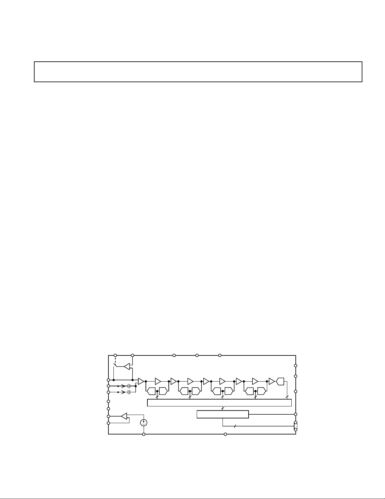
FUNCTIONAL BLOCK DIAGRAM
CMOS A/D Converter
AD9200
A single clock input is used to control all internal conversion
cycles. The digital output data is presented in straight binary
output format. An out-of-range signal (OTR) indicates an overflow condition which can be used with the most significant bit
to determine low or high overflow.
The AD9200 can operate with supply range from 2.7 V to
5.5 V, ideally suiting it for low power operation in high speed
portable applications.
The AD9200 is specified over the industrial (–40°C to +85°C)
and commercial (0°C to +70°C) temperature ranges.
PRODUCT HIGHLIGHTS
Low Power
The AD9200 consumes 80 mW on a 3 V supply (excluding the
reference power). In sleep mode, power is reduced to below
5 mW.
Very Small Package
The AD9200 is available in both a 28-lead SSOP and 48-lead
LQFP packages.
Pin Compatible with AD876
The AD9200 is pin compatible with the AD876, allowing older
designs to migrate to lower supply voltages.
300 MHz On-Board Sample-and-Hold
The versatile SHA input can be configured for either singleended or differential inputs.
Out-of-Range Indicator
The OTR output bit indicates when the input signal is beyond
the AD9200’s input range.
Built-In Clamp Function
Allows dc restoration of video signals with AD9200ARS and
AD9200KST.
CLAMP
CLAMP
AIN
REFTS
REFBS
REFTF
REFBF
VREF
REFSENSE
IN
SHA SHAGAIN SHA GAINGAIN
SHA
AVSS
1V
A/D
D/A
A/D
AD9200
REV. E
Information furnished by Analog Devices is believed to be accurate and
reliable. However, no responsibility is assumed by Analog Devices for its
use, nor for any infringements of patents or other rights of third parties
which may result from its use. No license is granted by implication or
otherwise under any patent or patent rights of Analog Devices.
DRVDDAVDDCLK
STBY
SHA GAIN
A/D
D/A A/D
CORRECTION LOGIC
OUTPUT BUFFERS
One Technology Way, P.O. Box 9106, Norwood, MA 02062-9106, U.S.A.
Tel: 781/329-4700 World Wide Web Site: http://www.analog.com
Fax: 781/326-8703 © Analog Devices, Inc., 1999
D/A
DRVSS
A/D
D/A
MODE
THREE-
STATE
OTR
D9
(MSB)
D0
(LSB)
Page 2

(AVDD = +3 V, DRVDD = +3 V, FS = 20 MHz (50% Duty Cycle), MODE = AVDD, 2 V Input
AD9200–SPECIFICATIONS
Span from 0.5 V to 2.5 V, External Reference, T
Parameter Symbol Min Typ Max Units Condition
RESOLUTION 10 Bits
CONVERSION RATE F
S
20 MHz
DC ACCURACY
Differential Nonlinearity DNL ±0.5 ±1 LSB REFTS = 2.5 V, REFBS = 0.5 V
Integral Nonlinearity INL ±0.75 ±2 LSB
Offset Error E
Gain Error E
ZS
FS
0.4 1.2 % FSR
1.4 3.5 % FSR
REFERENCE VOLTAGES
Top Reference Voltage REFTS 1 AVDD V
Bottom Reference Voltage REFBS GND AVDD – 1 V
Differential Reference Voltage 2 V p-p
Reference Input Resistance
1
10 kΩ REFTS, REFBS: MODE = AVDD
4.2 kΩ Between REFTF and REFBF: MODE = AVSS
ANALOG INPUT
Input Voltage Range AIN REFBS REFTS V REFBS Min = GND: REFTS Max = AVDD
Input Capacitance C
Aperture Delay t
Aperture Uncertainty (Jitter) t
IN
AP
AJ
1 pF Switched
4ns
2ps
Input Bandwidth (–3 dB) BW
Full Power (0 dB) 300 MHz
DC Leakage Current 23 µA Input = ±FS
INTERNAL REFERENCE
Output Voltage (1 V Mode) VREF 1 V REFSENSE = VREF
Output Voltage Tolerance (1 V Mode) ±10 ±25 mV
Output Voltage (2 V Mode) VREF 2 V REFSENSE = GND
Load Regulation (1 V Mode) 0.5 2 mV 1 mA Load Current
POWER SUPPLY
Operating Voltage AVDD 2.7 3 5.5 V
DRVDD 2.7 3 5.5 V
Supply Current IAVDD 26.6 33.3 mA AVDD = 3 V, MODE = AVSS
Power Consumption P
D
80 100 mW AVDD = DRVDD = 3 V, MODE = AVSS
Power-Down 4 mW STBY = AVDD, MODE and CLOCK =
AVSS
Gain Error Power Supply Rejection PSRR 1 % FS
DYNAMIC PERFORMANCE (AIN = 0.5 dBFS)
Signal-to-Noise and Distortion SINAD
f = 3.58 MHz 54.5 57 dB
f = 10 MHz 54 dB
Effective Bits
f = 3.58 MHz 9.1 Bits
f = 10 MHz 8.6 Bits
Signal-to-Noise SNR
f = 3.58 MHz 55 57 dB
f = 10 MHz 56 dB
Total Harmonic Distortion THD
f = 3.58 MHz –59 –66 dB
f = 10 MHz –58 dB
Spurious Free Dynamic Range SFDR
f = 3.58 MHz –61 –69 dB
f = 10 MHz –61 dB
Two-Tone Intermodulation
Distortion IMD 68 dB f = 44.49 MHz and 45.52 MHz
Differential Phase DP 0.1 Degree NTSC 40 IRE Mod Ramp
Differential Gain DG 0.05 %
MIN
to T
unless otherwise noted)
MAX
–2–
REV. E
Page 3
Parameter Symbol Min Typ Max Units Condition
DIGITAL INPUTS
High Input Voltage V
Low Input Voltage V
IH
IL
2.4 V
0.3 V
DIGITAL OUTPUTS
High-Z Leakage I
Data Valid Delay t
Data Enable Delay t
Data High-Z Delay t
OZ
OD
DEN
DHZ
–10 +10 µA Output = GND to VDD
25 ns CL = 20 pF
25 ns
13 ns
LOGIC OUTPUT (with DRVDD = 3 V)
High Level Output Voltage (I
High Level Output Voltage (I
Low Level Output Voltage (I
Low Level Output Voltage (I
= 50 µA) V
OH
= 0.5 mA) V
OH
= 1.6 mA) V
OL
= 50 µA) V
OL
OH
OH
OL
OL
+2.95 V
+2.80 V
+0.4 V
+0.05 V
LOGIC OUTPUT (with DRVDD = 5 V)
High Level Output Voltage (I
High Level Output Voltage (I
Low Level Output Voltage (I
Low Level Output Voltage (I
= 50 µA) V
OH
= 0.5 mA) V
OH
= 1.6 mA) V
OL
= 50 µA) V
OL
OH
OH
OL
OL
+4.5 V
+2.4 V
+0.4 V
+0.1 V
CLOCKING
Clock Pulsewidth High t
Clock Pulsewidth Low t
CH
CL
22.5 ns
22.5 ns
Pipeline Latency 3 Cycles
CLAMP
NOTES
1
2
Specifications subject to change without notice.
2
Clamp Error Voltage E
Clamp Pulsewidth t
See Figures 1a and 1b.
Available only in AD9200ARS and AD9200KST.
OC
CPW
±20 ±40 mV CLAMPIN = 0.5 V–2.7 V, RIN = 10 Ω
2 µsC
= 1 µF (Period = 63.5 µs)
IN
AD9200
REV. E
AV
DD
REFTS
REFBS
MODE
10kV
10kV
AD9200
0.4 3 V
DD
REFTS
REFTF
REFBF
REFBS
MODE
Figure 1a. Figure 1b.
–3–
AD9200
4.2kV
Page 4
AD9200
WARNING!
ESD SENSITIVE DEVICE
ABSOLUTE MAXIMUM RATINGS*
With
Respect
Parameter to Min Max Units
AVDD AVSS –0.3 +6.5 V
DRVDD DRVSS –0.3 +6.5 V
AVSS DRVSS –0.3 +0.3 V
AVDD DRVDD –6.5 +6.5 V
MODE AVSS –0.3 AVDD + 0.3 V
CLK AVSS –0.3 AVDD + 0.3 V
Digital Outputs DRVSS –0.3 DRVDD + 0.3 V
AIN AVSS –0.3 AVDD + 0.3 V
VREF AVSS –0.3 AVDD + 0.3 V
REFSENSE AVSS –0.3 AVDD + 0.3 V
REFTF, REFTB AVSS –0.3 AVDD + 0.3 V
REFTS, REFBS AVSS –0.3 AVDD + 0.3 V
Junction Temperature +150 °C
Storage Temperature –65 +150 °C
Lead Temperature
10 sec +300 °C
AVDD
DRVDD
AVDD
*Stresses above those listed under Absolute Maximum Ratings may cause perma-
nent damage to the device. This is a stress rating only; functional operation of the
device at these or any other conditions above those indicated in the operational
sections of this specification is not implied. Exposure to absolute maximum
ratings for extended periods may effect device reliability.
ORDERING GUIDE
Temperature Package Package
Model Range Description Options*
AD9200JRS 0°C to +70°C 28-Lead SSOP RS-28
AD9200ARS –40°C to +85°C 28-Lead SSOP RS-28
AD9200JST 0°C to +70°C 48-Lead LQFP ST-48
AD9200KST 0°C to +70°C 48-Lead LQFP ST-48
AD9200JRSRL 0°C to +70°C 28-Lead SSOP (Reel) RS-28
AD9200ARSRL –40°C to +85°C 28-Lead SSOP (Reel) RS-28
AD9200JSTRL 0°C to +70°C 48-Lead LQFP (Reel) ST-48
AD9200KSTRL 0°C to +70°C 48-Lead LQFP (Reel) ST-48
AD9200 SSOP-EVAL Evaluation Board
AD9200 LQFP-EVAL Evaluation Board
*RS = Shrink Small Outline; ST = Thin Quad Flatpack.
AVDD
AVDD
AVDD
DRVSS
DRVSS
AVSS
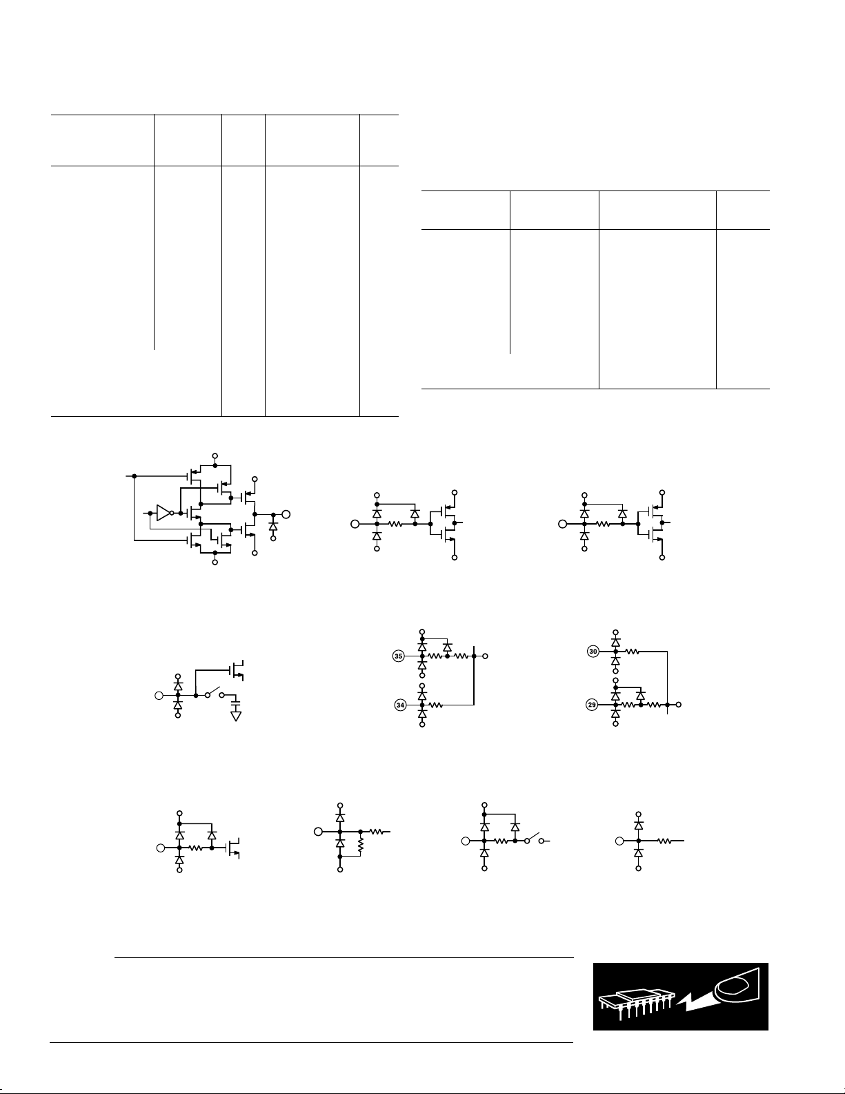
a. D0–D9, OTR
AVDD
AVSS
b. Three-State, Standby, Clamp
d. AIN
AVDD
AVSS
f. CLAMPIN g. MODE
AVDD
AVSS
AVSS
REFBS
REFBF
AVDD
AVDD
AVSS
AVSS
AVSS
e. Reference
AVDD
AVSS
h. REFSENSE
Figure 2. Equivalent Circuits
CAUTION
ESD (electrostatic discharge) sensitive device. Electrostatic charges as high as 4000 V readily
accumulate on the human body and test equipment and can discharge without detection.
Although the AD9200 features proprietary ESD protection circuitry, permanent damage may
occur on devices subjected to high energy electrostatic discharges. Therefore, proper ESD
precautions are recommended to avoid performance degradation or loss of functionality.
–4–
REFTF
REFTS
AVSS
AVDD
AVDD
AVSS
c. CLK
AVSS
AVSS
AVDD
AVSS
i. VREF
REV. E
Page 5
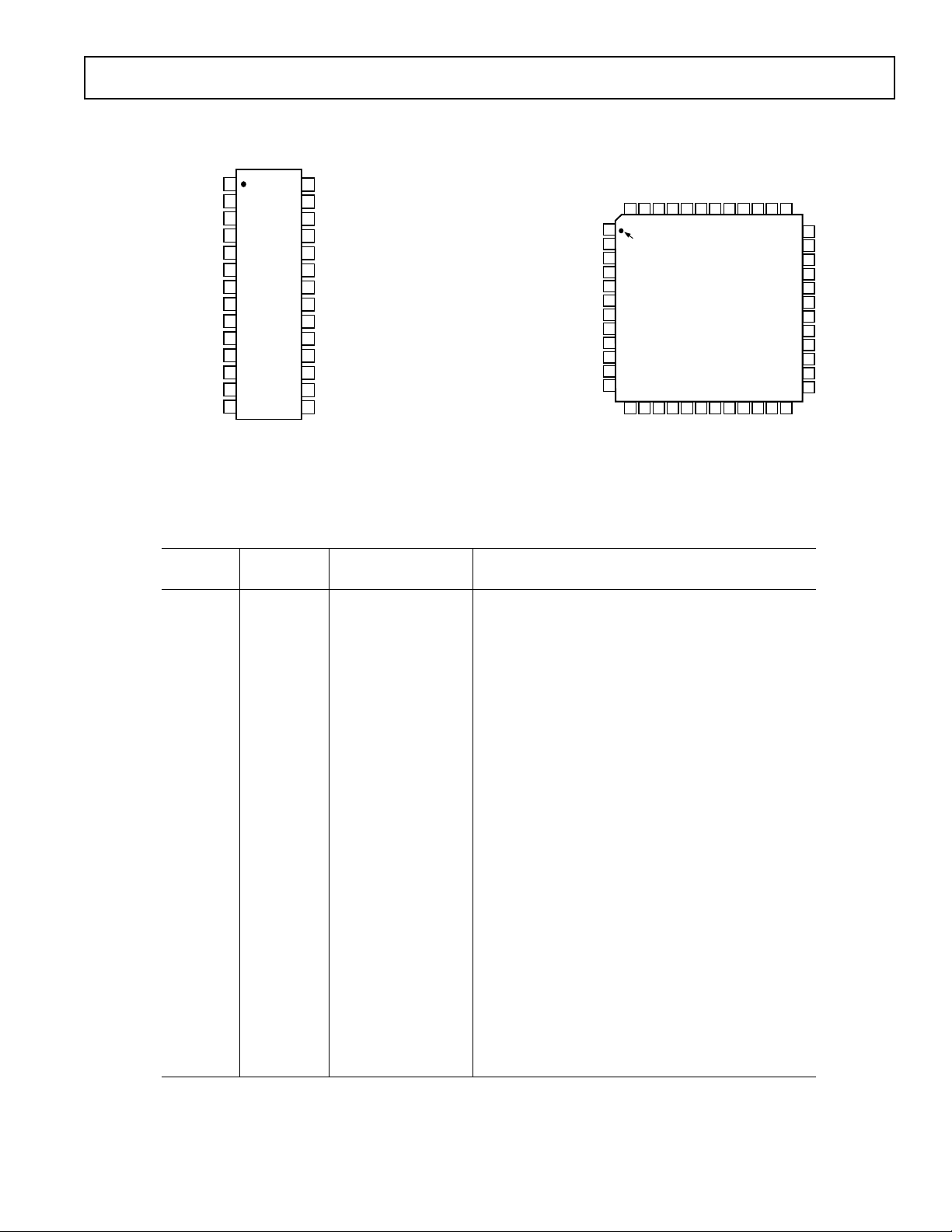
PIN CONFIGURATIONS
28-Lead Shrink Small Outline (SSOP)
AD9200
48-Lead Plastic Thin Quad Flatpack (LQFP)
AVSS
DRVDD
OTR
DRVSS
D0
D1
D2
D3
D4
D5
D6
D7
D8
D9
1
2
3
4
5
AD9200
6
TOP VIEW
(Not to Scale)
7
8
9
10
11
12
13
14
AVDD
28
AIN
27
VREF
26
REFBS
25
REFBF
24
23
MODE
REFTF
22
REFTS
21
20
CLAMPIN
19
CLAMP
18
REFSENSE
17
STBY
16
THREE-STATE
15
CLK
D0
D1
D2
D3
D4
NC
NC
D5
D6
D7
D8
D9
NC = NO CONNECT
NC
NC
DRVDD
NC
48 47 46 45 44 39 38 3743 42 41 40
1
PIN 1
2
IDENTIFIER
3
4
5
6
7
8
9
10
11
12
13 14 15 16 17 18 19 20 21 22 23 24
NC
NC
TOP VIEW
(Not to Scale)
NC
OTR
NC
AVSS
AD9200
NC
DRVSS
AVDD
NC
NC
NC
NC
NC
AIN
CLK
VREF
NC
36
35
34
33
32
31
30
29
28
27
26
25
STBY
THREE-STATE
PIN FUNCTION DESCRIPTIONS
SSOP LQFP
Pin No. Pin No. Name Description
1 44 AVSS Analog Ground
2 45 DRVDD Digital Driver Supply
3 1 D0 Bit 0, Least Significant Bit
4 2 D1 Bit 1
5 3 D2 Bit 2
6 4 D3 Bit 3
7 5 D4 Bit 4
8 8 D5 Bit 5
9 9 D6 Bit 6
10 10 D7 Bit 7
11 11 D8 Bit 8
12 12 D9 Bit 9, Most Significant Bit
13 16 OTR Out-of-Range Indicator
14 17 DRVSS Digital Ground
15 22 CLK Clock Input
16 23 THREE-STATE HI: High Impedance State. LO: Normal Operation
17 24 STBY HI: Power-Down Mode. LO: Normal Operation
18 26 REFSENSE Reference Select
19 27 CLAMP HI: Enable Clamp Mode. LO: No Clamp
20 28 CLAMPIN Clamp Reference Input
21 29 REFTS Top Reference
22 30 REFTF Top Reference Decoupling
23 32 MODE Mode Select
24 34 REFBF Bottom Reference Decoupling
25 35 REFBS Bottom Reference
26 38 VREF Internal Reference Output
27 39 AIN Analog Input
28 42 AVDD Analog Supply
NC
REFBS
REFBF
NC
MODE
NC
REFTF
REFTS
CLAMPIN
CLAMP
REFSENSE
NC
REV. E
–5–
Page 6
AD9200
DEFINITIONS OF SPECIFICATIONS
Integral Nonlinearity (INL)
Integral nonlinearity refers to the deviation of each individual
code from a line drawn from “zero” through “full scale”. The
point used as “zero” occurs 1/2 LSB before the first code transition. “Full scale” is defined as a level 1 1/2 LSB beyond the last
code transition. The deviation is measured from the center of
each particular code to the true straight line.
Differential Nonlinearity (DNL, No Missing Codes)
An ideal ADC exhibits code transitions that are exactly 1 LSB
apart. DNL is the deviation from this ideal value. It is often
specified in terms of the resolution for which no missing codes
(NMC) are guaranteed.
(AVDD = +3 V, DRVDD = +3 V, FS = 20 MHz (50% Duty Cycle), MODE = AVDD, 2 V Input
Typical Characterization Curves
1.0
0.5
0
DNL
Span from 0.5 V to 2.5 V, External Reference, unless otherwise noted)
Offset Error
The first transition should occur at a level 1 LSB above “zero.”
Offset is defined as the deviation of the actual first code transition from that point.
Gain Error
The first code transition should occur for an analog value 1 LSB
above nominal negative full scale. The last transition should
occur for an analog value 1 LSB below the nominal positive full
scale. Gain error is the deviation of the actual difference between first and last code transitions and the ideal difference
between the first and last code transitions.
Pipeline Delay (Latency)
The number of clock cycles between conversion initiation and
the associated output data being made available. New output
data is provided every rising edge.
60
55
50
45
40
SNR– dB
35
–0.5 AMPLITUDE
–6.0 AMPLITUDE
–20.0 AMPLITUDE
–0.5
–1.0
1.0
0.5
INL
–0.5
–1.0
0 1024128
0
0 1024128
256 384 512 640 768 896
CODE OFFSET
Figure 3. Typical DNL
256 384 512 640 768 896
CODE OFFSET
Figure 4. Typical INL
30
25
20
1.00E+05 1.00E+081.00E+06 1.00E+07
INPUT FREQUENCY – Hz
Figure 5. SNR vs. Input Frequency
60
55
50
45
40
SINAD – dB
35
30
25
20
1.00E+05 1.00E+081.00E+06
–0.5 AMPLITUDE
–6.0 AMPLITUDE
–20.0 AMPLITUDE
INPUT FREQUENCY – Hz
1.00E+07
Figure 6. SINAD vs. Input Frequency
–6–
REV. E
Page 7
AD9200
–30
–35
–40
–45
–50
–55
THD – dB
–60
–65
–70
–75
–80
1.00E+05 1.00E+081.00E+06 1.00E+07
–20.0 AMPLITUDE
–6.0 AMPLITUDE
–0.5 AMPLITUDE
INPUT FREQUENCY – Hz
Figure 7. THD vs. Input Frequency
–70
F
–60
–50
–40
–30
THD – dB
–20
–10
0
100E+03 100E+061E+06
CLOCK FREQUENCY – Hz
IN
= 1MHz
10E+06
CLOCK = 20MHz
80.5
80.5
80.0
80.0
79.5
79.5
79.0
79.0
78.5
78.5
78.0
78.0
POWER CONSUMPTION – mW
POWER CONSUMPTION – mW
77.5
77.5
77.0
77.0
0202
0202
4
6 8 10 12 14 16 18
4
6 8 10 12 14 16 18
CLOCK FREQUENCY – MHz
CLOCK FREQUENCY – MHz
Figure 10. Power Consumption vs. Clock Frequency
(MODE = AVSS)
1M
900k
800k
700k
600k
500k
HITS
400k
300k
200k
100k
54383
0
N–1 N
499856
CODE
54160
N+1
Figure 8. THD vs. Clock Frequency
1.005
1.004
1.003
1.002
– V
REF
V
1.001
1.000
0.999
0.998
–40 100–20
0
20 40 60 80
TEMPERATURE – °C
Figure 9. Voltage Reference Error vs. Temperature
Figure 11. Grounded Input Histogram
20
0
–20
–40
–60
–80
–100
–120
–140
0E+0 10E+61E+6 2E+6 3E+6 4E+6 5E+6 6E+6 7E+6 8E+6 9E+6
SINGLE TONE FREQUENCY DOMAIN
CLOCK = 20MHz
Figure 12. Single-Tone Frequency Domain
REV. E
–7–
Page 8
AD9200
0
–3
–6
–9
–12
–15
–18
SIGNAL AMPLITUDE – dB
–21
–24
–27
1.0E+6 1.0E+910.0E+6
FREQUENCY – Hz
100.0E+6
Figure 13. Full Power Bandwidth
25
20
15
10
5
0
– mA
B
I
–5
–10
–15
–20
–25
0 3.01.0 2.0
INPUT VOLTAGE – V
REFBS = 0.5V
REFTS = 2.5V
CLOCK = 20MHz
2.50.5 1.5
Figure 14. Input Bias Current vs. Input Voltage
APPLYING THE AD9200
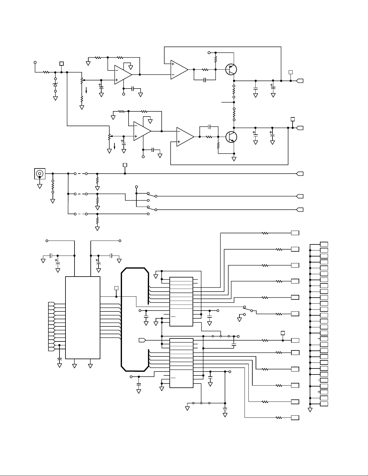
THEORY OF OPERATION
The AD9200 implements a pipelined multistage architecture to
achieve high sample rate with low power. The AD9200 distributes the conversion over several smaller A/D subblocks, refining
the conversion with progressively higher accuracy as it passes
the results from stage to stage. As a consequence of the distributed conversion, the AD9200 requires a small fraction of the
1023 comparators used in a traditional flash type A/D. A
sample-and-hold function within each of the stages permits the
first stage to operate on a new input sample while the second,
third and fourth stages operate on the three preceding samples.
OPERATIONAL MODES
The AD9200 is designed to allow optimal performance in a
wide variety of imaging, communications and instrumentation
applications, including pin compatibility with the AD876 A/D.
To realize this flexibility, internal switches on the AD9200 are
used to reconfigure the circuit into different modes. These modes
are selected by appropriate pin strapping. There are three parts
of the circuit affected by this modality: the voltage reference, the
reference buffer, and the analog input. The nature of the application will determine which mode is appropriate: the descriptions in the following sections, as well as the Table I should
assist in picking the desired mode.
Table I. Mode Selection
Input Input MODE REFSENSE
Modes Connect Span Pin Pin REF REFTS REFBS Figure
TOP/BOTTOM AIN 1 V AVDD Short REFSENSE, REFTS and VREF Together AGND 18
AIN 2 V AVDD AGND Short REFTS and VREF Together AGND 19
CENTER SPAN AIN 1 V AVDD/2 Short VREF and REFSENSE Together AVDD/2 AVDD/2 20
AIN 2 V AVDD/2 AGND No Connect AVDD/2 AVDD/2
Differential AIN Is Input 1 1 V AVDD/2 Short VREF and REFSENSE Together AVDD/2 AVDD/2 29
REFTS and
REFBS Are
Shorted Together
for Input 2 2 V AVDD/2 AGND No Connect AVDD/2 AVDD/2
External Ref AIN 2 V max AVDD AVDD No Connect Span = REFTS 21, 22
– REFBS (2 V max)
AGND Short to Short to 23
VREFTF VREFBF
AD876 AIN 2 V Float or AVDD No Connect Short to Short to 30
AVSS VREFTF VREFBF
–8–
REV. E
Page 9

SUMMARY OF MODES
VOLTAGE REFERENCE
1 V Mode the internal reference may be set to 1 V by connecting REFSENSE and VREF together.
2 V Mode the internal reference my be set to 2 V by connecting
REFSENSE to analog ground
External Divider Mode the internal reference may be set to a
point between 1 V and 2 V by adding external resistors. See
Figure 16f.
External Reference Mode enables the user to apply an external reference to REFTS, REFBS and VREF pins. This mode
is attained by tying REFSENSE to VDD.
REFERENCE BUFFER
Center Span Mode midscale is set by shorting REFTS and
REFBS together and applying the midscale voltage to that point
The MODE pin is set to AVDD/2. The analog input will swing
about that midscale point.
Top/Bottom Mode sets the input range between two points.
The two points are between 1 V and 2 V apart. The Top/Bottom
Mode is enabled by tying the MODE pin to AVDD.
ANALOG INPUT
Differential Mode is attained by driving the AIN pin as one
differential input and shorting REFTS and REFBS together and
driving them as the second differential input. The MODE pin
is tied to AVDD/2. Preferred mode for optimal distortion
performance.
Single-Ended is attained by driving the AIN pin while the
REFTS and REFBS pins are held at dc points. The MODE pin is
tied to AVDD.
Single-Ended/Clamped (AC Coupled) the input may be
clamped to some dc level by ac coupling the input. This is done
by tying the CLAMPIN to some dc point and applying a pulse
to the CLAMP pin. MODE pin is tied to AVDD.
SPECIAL
AD876 Mode enables users of the AD876 to drop the AD9200
into their socket. This mode is attained by floating or grounding
the MODE pin.
INPUT AND REFERENCE OVERVIEW
Figure 16, a simplified model of the AD9200, highlights the
relationship between the analog input, AIN, and the reference
voltages, REFTS, REFBS and VREF. Like the voltages applied
to the resistor ladder in a flash A/D converter, REFTS and
REFBS define the maximum and minimum input voltages to
the A/D.
The input stage is normally configured for single-ended operation, but allows for differential operation by shorting REFTS
and REFBS together to be used as the second input.
AD9200
AIN
REFTS
REFBS
Figure 15. AD9200 Equivalent Functional Input Circuit
SHA
In single-ended operation, the input spans the range,
REFBS ≤ AIN ≤ REFTS
where REFBS can be connected to GND and REFTS connected to VREF. If the user requires a different reference range,
REFBS and REFTS can be driven to any voltage within the
power supply rails, so long as the difference between the two is
between 1 V and 2 V.
In differential operation, REFTS and REFBS are shorted together, and the input span is set by VREF,
(REFTS – VREF/2) ≤ AIN ≤ (REFTS + VREF/2)
where VREF is determined by the internal reference or brought
in externally by the user.
The best noise performance may be obtained by operating the
AD9200 with a 2 V input range. The best distortion performance may be obtained by operating the AD9200 with a 1 V
input range.
REFERENCE OPERATION
The AD9200 can be configured in a variety of reference topologies. The simplest configuration is to use the AD9200’s onboard
bandgap reference, which provides a pin-strappable option to
generate either a 1 V or 2 V output. If the user desires a reference voltage other than those two, an external resistor divider
can be connected between VREF, REFSENSE and analog
ground to generate a potential anywhere between 1 V and 2 V.
Another alternative is to use an external reference for designs
requiring enhanced accuracy and/or drift performance. A
third alternative is to bring in top and bottom references,
bypassing VREF altogether.
Figures 16d, 16e and 16f illustrate the reference and input architecture of the AD9200. In tailoring a desired arrangement,
the user can select an input configuration to match drive circuit.
Then, moving to the reference modes at the bottom of the
figure, select a reference circuit to accommodate the offset and
amplitude of a full-scale signal.
Table I outlines pin configurations to match user requirements.
AD9200
A/D
CORE
REV. E
–9–
Page 10

AD9200
+FS
–FS
+F/S RANGE OBTAINED
FROM VREF PIN OR
EXTERNAL REF
–F/S RANGE OBTAINED
FROM VREF PIN OR
EXTERNAL REF
AIN
REFTS
REFBS
AD9200
SHA
10kV
10kV
A2
A/D
10kV
10kV
CORE
a. Top/Bottom Mode
MAXIMUM MAGNITUDE OF V
IS DETERMINED BY INTERNAL
REFERENCE AND TURNS RATIO
V
4.2kV
TOTAL
AVDD/2
REFTS
REFBS
AIN
MODE
(AVDD)
REFTF
0.1mF
REFBF
0.1mF
10mF
0.1mF
10kV
10kV
10kV
A2
MIDSCALE
SHA
A/D
CORE
V*
AIN
REFTS
REFBS
MIDSCALE OFFSET
VOLTAGE IS DERIVED
FROM INTERNAL OR
EXTERNAL REF
AD9200
4.2kV
TOTAL
MODE
REFTF
0.1mF
AD9200
SHA
10kV
10kV
A2
A/D
10kV
INTERNAL
REF
* MAXIMUM MAGNITUDE OF V IS DETERMINED
CORE
10kV
BY INTERNAL REFERENCE
b. Center Span Mode
AVDD/2
0.1mF
10mF
4.2kV
TOTAL
MODE
REFTF
0.1mF
REFBF
AVDD/2
0.1mF
10mF
0.1mF
A1
1V
AD9200
d. 1 V Reference
A1
1V
AD9200
INTERNAL 10K REF RESISTORS ARE
SWITCHED OPEN BY THE PRESENSE
OF R
AND RB.
A
f. Variable Reference
(Between 1 V and 2 V)
VREF
(1V)
REFSENSE
AVSS
VREF
(= 1 + R
R
A
REFSENSE
R
B
AVSS
A/RB
)
INTERNAL
c. Differential Mode
0.1mF 1.0mF
0.1mF 1.0mF
REF
10kV
0.1mF
REFBF
VREF
(2V)
1V
AD9200
A1
10kV
10kV
0.01mF 1.0mF
REFSENSE
AVSS
e. 2 V Reference
1V
AD9200
A1
VREF
g. Internal Reference Disable
(Power Reduction)
REFSENSE
AVDD
Figure 16.
–10–
REV. E
Page 11

AD9200
The actual reference voltages used by the internal circuitry of
the AD9200 appear on REFTF and REFBF. For proper operation, it is necessary to add a capacitor network to decouple these
pins. The REFTF and REFBF should be decoupled for all
internal and external configurations as shown in Figure 17.
REFTF
0.1mF
0.1mF
10mF
0.1mF
AD9200
REFBF
Figure 17. Reference Decoupling Network
Note: REFTF = reference top, force
REFBF = reference bottom, force
REFTS = reference top, sense
REFBS = reference bottom, sense
INTERNAL REFERENCE OPERATION
Figures 18, 19 and 20 show example hookups of the AD9200
internal reference in its most common configurations. (Figures
18 and 19 illustrate top/bottom mode while Figure 20 illustrates
center span mode). Figure 29 shows how to connect the AD9200
for 1 V p-p differential operation. Shorting the VREF pin
directly to the REFSENSE pin places the internal reference
amplifier, A1, in unity-gain mode and the resultant reference
output is 1 V. In Figure 18 REFBS is grounded to give an input
range from 0 V to 1 V. These modes can be chosen when the
supply is either +3 V or +5 V. The VREF pin must be bypassed to
AVSS (analog ground) with a 1.0 µF tantalum capacitor in
parallel with a low inductance, low ESR, 0.1 µF ceramic capacitor.
Figure 19 shows the single-ended configuration for 2 V p-p
operation. REFSENSE is connected to GND, resulting in a 2 V
reference output.
2V
0V
1.0mF
REFTS
REFBS
0.1mF
SENSE
AIN
VREF
REF
10kV
10kV
A1
10kV
A2
10kV
SHA
1V
A/D
CORE
AD9200
4.2kV
TOTAL
MODE
REFTF
0.1mF
REFBF
AVDD
0.1mF
10mF
0.1mF
Figure 19. Internal Reference, 2 V p-p Input Span
(Top/Bottom Mode)
Figure 20 shows the single-ended configuration that gives the
good high frequency dynamic performance (SINAD, SFDR).
To optimize dynamic performance, center the common-mode
voltage of the analog input at approximately 1.5 V. Connect the
shorted REFTS and REFBS inputs to a low impedance 1.5 V
source. In this configuration, the MODE pin is driven to a voltage at midsupply (AVDD/2).
Maximum reference drive is 1 mA. An external buffer is required for heavier loads.
1V
0V
0.1mF1.0mF
AIN
REFTS
REFBS
VREF
REF
SENSE
10kV
10kV
A1
10kV
A2
10kV
SHA
1V
A/D
CORE
AD9200
4.2kV
TOTAL
MODE
REFTF
0.1mF
REFBF
Figure 18. Internal Reference 1 V p-p Input Span
(Top/Bottom Mode)
AVDD
0.1mF
10mF
0.1mF
1.0mF
2V
1V
+1.5V
0.1mF
AIN
REFTS
REFBS
VREF
REF
SENSE
10kV
10kV
A1
10kV
A2
10kV
SHA
1V
A/D
CORE
AD9200
4.2kV
TOTAL
MODE
REFTF
0.1mF
REFBF
AVDD/2
Figure 20. Internal Reference 1 V p-p Input Span,
(Center Span Mode)
0.1mF
10mF
0.1mF
REV. E
–11–
Page 12

AD9200
EXTERNAL REFERENCE OPERATION
Using an external reference may provide more flexibility and
improve drift and accuracy. Figures 21 through 23 show examples of how to use an external reference with the AD9200.
To use an external reference, the user must disable the internal
reference amplifier by connecting the REFSENSE pin to VDD.
The user then has the option of driving the VREF pin, or driving the REFTS and REFBS pins.
The AD9200 contains an internal reference buffer (A2), that
simplifies the drive requirements of an external reference. The
external reference must simply be able to drive a 10 kΩ load.
Figure 21 shows an example of the user driving the top and bottom
references. REFTS is connected to a low impedance 2 V source
and REFBS is connected to a low impedance 1 V source. REFTS
and REFBS may be driven to any voltage within the supply as
long as the difference between them is between 1 V and 2 V.
2V
1V
2V
1V
AVDD
AIN
REFTS
REFBS
REF
SENSE
MODE
10kV
10kV
10kV
A2
10kV
SHA
A/D
CORE
AD9200
4.2kV
TOTAL
REFTF
0.1mF
REFBF
0.1mF
10mF
0.1mF
4V
2V
4V
2V
0.1 F
10 F
AVDD
0.1 F
0.1 F
VIN
REFTS
REFTF
AD9200
REFBF
REFBS
VREF
REFSENSE
MODE
Figure 23a. External Reference—2 V p-p Input Span
REFT
REFB
+5V
6
5
2
3
C4
F
0.1
8
7
C3
F
0.1
C2
F
10
C5
0.1 F
6
4
C1
0.1
F
C6
0.1
F
REFTS
REFTF
AD9200
REFBS
REFBF
Figure 23b. Kelvin Connected Reference Using the AD9200
Figure 21. External Reference Mode—1 V p-p Input Span
Figure 22 shows an example of an external reference generating
2.5 V at the shorted REFTS and REFBS inputs. In this instance, a REF43 2.5 V reference drives REFTS and REFBS. A
resistive divider generates a 1 V VREF signal that is buffered by
A3. A3 must be able to drive a 10 kΩ, capacitive load. Choose
this op amp based on noise and accuracy requirements.
3.0V
2.5V
2.0V
10mF
0.1mF
REF43
1.5kV
1kV
A3
+5V
0.1mF
1.0mF
AVDD/2
0.1mF
0.1mF
AVDD
AD9200
AIN
REFTS
REFBS
VREF
MODE
REFSENSE
AVDD
REFTF
REFBF
0.1mF
AVDD
0.1mF
10mF
0.1mF
Figure 22. External Reference Mode—1 V p-p Input
Span 2.5 V
CM
Figure 23a shows an example of the external references driving
the REFTF and REFBF pins that is compatible with the
AD876. REFTS is shorted to REFTF and driven by an external
4 V low impedance source. REFBS is shorted to REFBF and
driven by a 2 V source. The MODE pin is connected to GND
in this configuration.
STANDBY OPERATION
The ADC may be placed into a powered down (sleep) mode by
driving the STBY (standby) pin to logic high potential and
holding the clock at logic low. In this mode the typical power
drain is approximately 4 mW. If there is no connection to the
STBY pin, an internal pull-down circuit will keep the ADC in a
“wake-up” mode of operation.
The ADC will “wake up” in 400 ns (typ) after the standby pulse
goes low.
CLAMP OPERATION
The AD9200ARS and AD9200KST parts feature an optional
clamp circuit for dc restoration of video or ac coupled signals.
Figure 24 shows the internal clamp circuitry and the external
control signals needed for clamp operation. To enable the
clamp, apply a logic high to the CLAMP pin. This will close
the switch SW1. The clamp amplifier will then servo the voltage at the AIN pin to be equal to the clamp voltage applied at
the CLAMPIN pin. After the desired clamp level is attained,
SW1 is opened by taking CLAMP back to a logic low. Ignoring
the droop caused by the input bias current, the input capacitor
CIN will hold the dc voltage at AIN constant until the next
clamp interval. The input resistor RIN has a minimum recom-
mended value of 10 Ω, to maintain the closed-loop stability of
the clamp amplifier.
The allowable voltage range that can be applied to CLAMPIN
depends on the operational limits of the internal clamp amplifier. When operating off of 3 volt supplies, the recommended
clamp range is between 0.5 volts and 2.0 volts.
–12–
REV. E
Page 13

AD9200
The input capacitor should be sized to allow sufficient acquisition time of the clamp voltage at AIN within the CLAMP interval, but also be sized to minimize droop between clamping
intervals. Specifically, the acquisition time when the switch is
closed will equal:
V
T
= R
ACQ
INCIN
C
ln
V
E
where VC is the voltage change required across CIN, and VE is
the error voltage. V
is calculated by taking the difference be-
C
tween the initial input dc level at the start of the clamp interval
and the clamp voltage supplied at CLAMPIN. V
is a system-
E
dependent parameter, and equals the maximum tolerable deviation from V
. For example, if a 2-volt input level needs to be
C
clamped to 1 volt at the AD9200’s input within 10 millivolts,
then V
equals 2 – 1 or 1 volt, and VE equals 10 mV. Note that
C
once the proper clamp level is attained at the input, only a very
small voltage change will be required to correct for droop.
The voltage droop is calculated with the following equation:
I
BIAS
dV =
t
()
C
IN
where t = time between clamping intervals.
The bias current of the AD9200 will depend on the sampling
rate, F
over time, with an input resistance equal to 1/C
. The switched capacitor input AIN appears resistive
S
. Given a
SFS
sampling rate of 20 MSPS and an input capacitance of 1 pF, the
input resistance is 50 kΩ. This input resistance is equivalently
terminated at the midscale voltage of the input range. The worst
case bias current will thus result when the input signal is at the
extremes of the input range, that is, the furthest distance from
the midscale voltage level. For a 1-volt input range, the maxi-
mum bias current will be ±0.5 volts divided by 50 kΩ, which is
±10 µA.
If droop is a critical parameter, then the minimum value of C
IN
should be calculated first based on the droop requirement.
Acquisition time—the width of the CLAMP pulse—can be
adjusted accordingly once the minimum capacitor value is chosen. A tradeoff will often need to be made between droop and
acquisition time, or error voltage V
.
E
Clamp Circuit Example
A single supply video amplifier outputs a level-shifted video
signal between 2 and 3 volts with the following parameters:
horizontal period = 63.56 µs,
horizontal sync interval = 10.9 µs,
horizontal sync pulse = 4.7 µs,
sync amplitude = 0.3 volts,
video amplitude of 0.7 volts,
reference black level = 2.3 volts
The video signal must be dc restored from a 2- to 3-volt range
down to a 1- to 2-volt range. Configuring the AD9200 for a
one volt input span with an input range from 1 to 2 volts (see
Figure 24), the CLAMPIN voltage can be set to 1 volt with an
external voltage or by direct connection to REFBS. The CLAMP
pulse may be applied during the SYNC pulse, or during the
back porch to truncate the SYNC below the AD9200’s minimum input voltage. With a C
= 1 µF, and RIN = 20 Ω, the
IN
acquisition time needed to set the input dc level to one volt
with 1 mV accuracy is about 140 µs, assuming a full 1 volt V
.
C
With a 1 µF input coupling capacitor, the droop across one
horizontal can be calculated:
I
= 10 µA, and t = 63.5 µs, so dV = 0.635 mV, which is less
BIAS
than one LSB.
After the input capacitor is initially charged, the clamp pulsewidth only needs to be wide enough to correct small voltage
errors such as the droop. The fine scale settling characteristics
of the clamp circuitry are shown in Table II.
Depending on the required accuracy, a CLAMP pulsewidth of
1 µs–3 µs should work in most applications. The OFFSET val-
ues ignore the contribution of offset from the clamp amplifier;
they simply compare the output code with a “final value” measured with a much longer CLAMP pulse duration.
Table II.
CLAMP OFFSET
10 µs <1 LSB
5 µs 5 LSBs
4 µs 7 LSBs
3 µs 11 LSBs
2 µs 19 LSBs
1 µs 42 LSBs
AD9200
CLAMP IN
CIN
RIN
CLAMP
AIN
SW1
TO
SHA
Figure 24a. Clamp Operation
AIN
0.1 F
0.1 F
SHORT TO REFBS
OR EXTERNAL DC
10
AVDD
2
F
0.1 F
REFTF
REFTS
AD9200
REFBF
REFBS
MODE
CLAMP
CLAMPIN
Figure 24b. Video Clamp Circuit
REV. E
–13–
Page 14

AD9200
DRIVING THE ANALOG INPUT
Figure 25 shows the equivalent analog input of the AD9200, a
sample-and-hold amplifier (switched capacitor input SHA).
Bringing CLK to a logic low level closes Switches 1 and 2 and
opens Switch 3. The input source connected to AIN must
charge capacitor CH during this time. When CLK transitions
from logic “low” to logic “high,” Switches 1 and 2 open, placing
the SHA in hold mode. Switch 3 then closes, forcing the output
of the op amp to equal the voltage stored on CH. When CLK
transitions from logic “high” to logic “low,” Switch 3 opens
first. Switches 1 and 2 close, placing the SHA in track mode.
The structure of the input SHA places certain requirements on
the input drive source. The combination of the pin capacitance,
CP, and the hold capacitance, CH, is typically less than 5 pF.
The input source must be able to charge or discharge this capacitance to 10-bit accuracy in one half of a clock cycle. When
the SHA goes into track mode, the input source must charge or
discharge capacitor CH from the voltage already stored on CH
to the new voltage. In the worst case, a full-scale voltage step on
the input, the input source must provide the charging current
through the R
(50 Ω) of Switch 1 and quickly (within 1/2 CLK
ON
period) settle. This situation corresponds to driving a low input
impedance. On the other hand, when the source voltage equals
the value previously stored on CH, the hold capacitor requires
no input current and the equivalent input impedance is extremely high.
Adding series resistance between the output of the source and
the AIN pin reduces the drive requirements placed on the
source. Figure 26 shows this configuration. The bandwidth of
the particular application limits the size of this resistor. To
maintain the performance outlined in the data sheet specifica-
tions, the resistor should be limited to 20 Ω or less. For applica-
tions with signal bandwidths less than 10 MHz, the user may
proportionally increase the size of the series resistor. Alternatively, adding a shunt capacitance between the AIN pin and
analog ground can lower the ac load impedance. The value of
this capacitance will depend on the source resistance and the
required signal bandwidth.
The input span of the AD9200 is a function of the reference
voltages. For more information regarding the input range, see
the Internal and External Reference sections of the data sheet.
CH
AIN
(REFTS
REFBS)
CP
CP
S1
S3
S2
AD9200
SHA
CH
Figure 25. AD9200 Equivalent Input Structure
In many cases, particularly in single-supply operation, ac coupling offers a convenient way of biasing the analog input signal
at the proper signal range. Figure 25 shows a typical configuration for ac-coupling the analog input signal to the AD9200.
Maintaining the specifications outlined in the data sheet
requires careful selection of the component values. The most
important is the f
R2 and the parallel combination of C1 and C2. The f
high-pass corner frequency. It is a function of
–3 dB
–3 dB
point
can be approximated by the equation:
f
where C
= 1/(2 × pi × [R2] C
–3 dB
is the parallel combination of C1 and C2. Note that
EQ
EQ
)
C1 is typically a large electrolytic or tantalum capacitor that
becomes inductive at high frequencies. Adding a small ceramic
or polystyrene capacitor (on the order of 0.01 µF) that does not
become inductive until negligibly higher frequencies, maintains
a low impedance over a wide frequency range.
NOTE: AC coupled input signals may also be shifted to a desired
level with the AD9200’s internal clamp. See Clamp Operation.
V
C1
IN
C2
R1
R2
V
BIAS
AIN
I
B
AD9200
Figure 27. AC Coupled Input
There are additional considerations when choosing the resistor
values. The ac-coupling capacitors integrate the switching transients present at the input of the AD9200 and cause a net dc
bias current, I
, to flow into the input. The magnitude of the
B
bias current increases as the signal magnitude deviates from
V midscale and the clock frequency increases; i.e., minimum
bias current flow when AIN = V midscale. This bias current
will result in an offset error of (R1 + R2) × I
. If it is necessary
B
to compensate this error, consider making R2 negligibly small or
modifying VBIAS to account for the resultant offset.
In systems that must use dc coupling, use an op amp to levelshift a ground-referenced signal to comply with the input requirements of the AD9200. Figure 28 shows an AD8041 configured in noninverting mode.
+V
CC
0.1 F
MIDSCALE
OFFSET
VOLTAGE
NC
0V
1V p-p
DC
2
AD8041
3
7
1
5
4
NC
20
6
AD9200
AIN
<
20V
AIN
V
S
AD9200
Figure 26. Simple AD9200 Drive Configuration
–14–
Figure 28. Bipolar Level Shift
REV. E
Page 15

AD9200
DIFFERENTIAL INPUT OPERATION
The AD9200 will accept differential input signals. This function
may be used by shorting REFTS and REFBS and driving them
as one leg of the differential signal (the top leg is driven into
AIN). In the configuration below, the AD9200 is accepting a
1 V p-p signal. See Figure 29.
2V
1V
1.0mF
AVDD/2
0.1mF
AVDD/2
AD9200
AIN
REFTS
REFBS
VREF
REFSENSE
MODE
REFTF
REFBF
0.1mF
0.1mF
10mF
0.1mF
Figure 29. Differential Input
AD876 MODE OF OPERATION
The AD9200 may be dropped into the AD876 socket. This will
allow AD876 users to take advantage of the reduced power
consumption realized when running the AD9200 on a 3.0 V
analog supply.
Figure 30 shows the pin functions of the AD876 and AD9200.
The grounded REFSENSE pin and floating MODE pin effectively put the AD9200 in the external reference mode. The
external reference input for the AD876 will now be placed on
the reference pins of the AD9200.
The clamp controls will be grounded by the AD876 socket. The
AD9200 has a 3 clock cycle delay compared to a 3.5 cycle delay
of the AD876.
4V
2V
4V
2V
10mF
0.1mF
0.1mF
0.1mF
AVDD
AIN
AD9200
REFTS
REFTF
REFBF
REFBS
MODENC
REFSENSE
CLAMP
CLAMPIN
OTR
VREF
0.1mF
The pipelined architecture of the AD9200 operates on both
rising and falling edges of the input clock. To minimize duty
cycle variations the recommended logic family to drive the clock
input is high speed or advanced CMOS (HC/HCT, AC/ACT)
logic. CMOS logic provides both symmetrical voltage threshold
levels and sufficient rise and fall times to support 20 MSPS
operation. The AD9200 is designed to support a conversion rate
of 20 MSPS; running the part at slightly faster clock rates may
be possible, although at reduced performance levels. Conversely,
some slight performance improvements might be realized by
clocking the AD9200 at slower clock rates.
ANALOG
INPUT
INPUT
CLOCK
DATA
OUTPUT
S1
t
CH
S2
t
C
t
CL
S3
S4
25ns
DATA 1
Figure 31. Timing Diagram
The power dissipated by the output buffers is largely proportional to the clock frequency; running at reduced clock rates
provides a reduction in power consumption.
DIGITAL INPUTS AND OUTPUTS
Each of the AD9200 digital control inputs, THREE-STATE
and STBY are reference to analog ground. The clock is also
referenced to analog ground.
The format of the digital output is straight binary (see Figure
32). A low power mode feature is provided such that for STBY
= HIGH and the clock disabled, the static power of the AD9200
will drop below 5 mW.
OTR
–FS+1LSB
–FS
+FS
+FS–1LSB
Figure 32. Output Data Format
Figure 30. AD876 Mode
CLOCK INPUT
The AD9200 clock input is buffered internally with an inverter
powered from the AVDD pin. This feature allows the AD9200
to accommodate either +5 V or +3.3 V CMOS logic input signal swings with the input threshold for the CLK pin nominally
at AVDD/2.
REV. E
–15–
THREE-
STATE
DATA
(D0–D9)
t
DHZ
HIGH
IMPEDANCE
t
DEN
Figure 33. Three-State Timing Diagram
Page 16

AD9200
APPLICATIONS
DIRECT IF DOWN CONVERSION USING THE AD9200
Sampling IF signals above an ADC’s baseband region (i.e., dc
to F
/2) is becoming increasingly popular in communication
S
applications. This process is often referred to as Direct IF Down
Conversion or Undersampling. There are several potential benefits in using the ADC to alias (i.e., or mix) down a narrowband
or wideband IF signal. First and foremost is the elimination of a
complete mixer stage with its associated amplifiers and filters,
reducing cost and power dissipation. Second is the ability to
apply various DSP techniques to perform such functions as
filtering, channel selection, quadrature demodulation, data
reduction, detection, etc. A detailed discussion on using this
technique in digital receivers can be found in Analog Devices
Application Notes AN-301 and AN-302.
In Direct IF Down Conversion applications, one exploits the
inherent sampling process of an ADC in which an IF signal
lying outside the baseband region can be aliased back into the
baseband region in a similar manner that a mixer will downconvert an IF signal. Similar to the mixer topology, an image
rejection filter is required to limit other potential interfering
signals from also aliasing back into the ADC’s baseband region.
A tradeoff exists between the complexity of this image rejection
filter and the sample rate as well as dynamic range of the ADC.
The AD9200 is well suited for various narrowband IF sampling
applications. The AD9200’s low distortion input SHA has a
full-power bandwidth extending to 300 MHz thus encompassing
many popular IF frequencies. A DNL of ±0.5 LSB (typ) com-
bined with low thermal input referred noise allows the AD9200 in
the 2 V span to provide 60 dB of SNR for a baseband input sine
wave. Also, its low aperture jitter of 2 ps rms ensures minimum
SNR degradation at higher IF frequencies. In fact, the AD9200
is capable of still maintaining 56 dB of SNR at an IF of 135 MHz
with a 1 V (i.e., 4 dBm) input span. Note, although the AD9200
will typically yield a 3 to 4 dB improvement in SNR when configured for the 2 V span, the 1 V span provides the optimum
full-scale distortion performance. Furthermore, the 1 V span
reduces the performance requirements of the input driver circuitry and thus may be more practical for system implementation purposes.
Figure 34 shows a simplified schematic of the AD9200 configured in an IF sampling application. To reduce the complexity of
the digital demodulator in many quadrature demodulation applications, the IF frequency and/or sample rate are selected such
that the bandlimited IF signal aliases back into the center of the
ADC’s baseband region (i.e., F
/4). For example, if an IF sig-
S
nal centered at 45 MHz is sampled at 20 MSPS, an image of
this IF signal will be aliased back to 5.0 MHz which corresponds to one quarter of the sample rate (i.e., F
/4). This
S
demodulation technique typically reduces the complexity of the
post digital demodulator ASIC which follows the ADC.
To maximize its distortion performance, the AD9200 is configured in the differential mode with a 1 V span using a transformer.
The center tap of the transformer is biased at midsupply via a
resistor divider. Preceding the AD9200 is a bandpass filter as
well as a 32 dB gain stage. A large gain stage may be required
to compensate for the high insertion losses of a SAW filter used
for image rejection. The gain stage will also provide adequate
isolation for the SAW filter from the charge “kick back” currents
associated with AD9200’s input stage.
The gain stage can be realized using one or two cascaded
AD8009 op amps amplifiers. The AD8009 is a low cost, 1 GHz,
current-feedback op amp having a 3rd order intercept characterized up to 250 MHz. A passive bandpass filter following the
AD8009 attenuates its dominant 2nd order distortion products
which would otherwise be aliased back into the AD9200’s
baseband region. Also, it reduces any out-of-band noise which
would also be aliased back due to the AD9200’s noise bandwidth of 220+ MHz. Note, the bandpass filters specifications
are application dependent and will affect both the total distortion and noise performance of this circuit.
The distortion and noise performance of an ADC at the given
IF frequency is of particular concern when evaluating an ADC
for a narrowband IF sampling application. Both single-tone and
dual-tone SFDR vs. amplitude are very useful in an assessing an
ADC’s noise performance and noise contribution due to aperture jitter. In any application, one is advised to test several units
of the same device under the same conditions to evaluate the
given applications sensitivity to that particular device.
SAW
FILTER
OUTPUT
50V
G
= 20dB G2 = 12dB L-C
1
200V
22.1V
50V
280V
93.1V
50V
BANDPASS
FILTER
MINI CIRCUITS
T4 - 6T
AVDD
1:4
1kV
1kV
Figure 34. Simplified AD9200 IF Sampling Circuit
–16–
200V
0.1mF
AD9200
AIN
REFTS
REFBS
VREF
0.1mF1.0mF
REFSENSE
REV. E
Page 17

AD9200
90
80
0
–60 0–40 –20
70
60
30
20
INPUT POWER LEVEL – dBFS
50
40
10
–10–50 –30
WORST CASE SPURIOUS – dBFS
SNR – dBc
SINGLE TONE SFDR
DUAL TONE SFDR
SNR
CLK = 20MSPS
SINGLE TONE – 85.52MHz
DUAL TONE– F
1
= 84.49MHz
– F
2
= 85.52MHz
Figures 35–38 combine the dual-tone SFDR as well as single
tone SFDR and SNR performance at IF frequencies of 45 MHz,
70 MHz, 85 MHz and 135 MHz. Note, the SFDR vs. amplitude data is referenced to dBFS while the single tone SNR data
is referenced to dBc. The performance characteristics in these
figures are representative of the AD9200 without the AD8009.
The AD9200 was operated in the differential mode (via transformer) with a 1 V span at 20 MSPS. The analog supply
(AVDD) and the digital supply (DRVDD) were set to +5 V and
3.3 V, respectively.
90
80
70
60
50
40
SNR – dBc
30
20
WORST CASE SPURIOUS – dBFS
10
0
–60 0–40 –20
DUAL TONE SFDR
SINGLE TONE SFDR
SNR
INPUT POWER LEVEL – dBFS
CLK = 20MSPS
SINGLE TONE – 45.52MHz
DUAL TONE– F
= 44.49MHz
1
– F
= 45.52MHz
2
–10–50 –30
Although not presented, data was also taken with the insertion
of an AD8009 gain stage of 32 dB in the signal path. No
degradation in two-tone SFDR vs. amplitude was noted at an
IF of 45 MHz, 70 MHz and 85 MHz. However, at 135 MHz,
the AD8009 became the limiting factor in the distortion performance until the two input tones were decreased to –15 dBFS
from their full-scale level of –6.5 dBFS. Note: the SNR performance in each case degraded by approximately 0.5 dB due to
the AD8009’s in-band noise contribution.
Figure 35. SNR/SFDR for IF @ 45 MHz
90
80
70
60
50
40
SNR – dBc
30
20
WORST CASE SPURIOUS – dBFS
10
0
–60 0–40 –20
Figure 36. SNR/SFDR for IF @ 70 MHz
REV. E
SINGLE TONE SFDR
DUAL TONE SFDR
SNR
INPUT POWER LEVEL – dBFS
CLK = 21.538MSPS
SINGLE TONE – 70.55MHz
DUAL TONE– F
= 69.50MHz
1
= 70.55MHz
– F
2
–10–50 –30
–17–
Figure 37. SNR/SFDR for IF @ 85 MHz
90
80
70
60
50
40
SNR – dBc
30
20
WORST CASE SPURIOUS – dBFS
10
0
–60 0–40 –20
DUAL TONE SFDR
SINGLE TONE SFDR
SNR
CLK = 20MSPS
SINGLE TONE – 135.52MHz
DUAL TONE – F1 = 134.44MHz
INPUT POWER LEVEL – dBFS
– F
= 135.52MHz
2
Figure 38. SNR/SFDR for IF @ 135 MHz
–10–50 –30
Page 18
AD9200
+3–5A
5.49kV
AD1580
J7
AVDD
DUTCLK
THREE-STATE
STBY
REFSENSE
CLAMP
CLAMPIN
REFTS
REFTF
MODE
REFBF
REFBS
VREF
AIN
R7
D1
GND
C16
0.1mF
10/10V
C33
TP14
R53
49.9V
+
C17
10/10V
15
16
17
18
19
20
21
22
23
24
25
26
27
XXXX
ADJ.
R8
10kV
CW
R9
1.5kV
JP5
JP17
JP18
28
AVDD
DRVDD
U1
AD9200
CLK
THREE-STATE
STBY
REFSENSE
CLAMP
CLAMPIN
REFTS
REFTF
MODE
REFBF
REFBS
VREF
AIN
AVSS
DRVSS
1
XXXX
ADJ.
R14
10kV
R37
1kV
R38
1kV
R39
1kV
C18
10/10V
WHITE
13
3
4
5
6
7
8
9
10
11
12
3
C8
10/10V
C19
0.1mF
D0
D1
D2
D3
D4
D5
D6
D7
D8
D9
R11
15kV
2
CW
OTR
TP19
AD822
U2
+3–5A
R12
10kV
TP11
DRVDD
DRVDD
4
C7
8
0.1mF
2
3
C9
10/10V
DRVDD
DRVDD
CLK
1
0.1mF
11kV
AD822
U3
+3–5A
C40
GND
R13
B
B
GND
C41
0.1mF
4
8
1
3
1
3
A
1
C10
0.1mF
S3
A
S4
GND
2
2
D5
D6
D7
D8
D9
D0
D1
D2
D3
D4
GND
5
AD822
U2
6
6
AD822
U3
5
16
B
U4 A
15
B
U4 A
21
B
U4 A
20
B
U4 A
19
B
U4 A
18
B
U4 A
17
B
U4 A
14
B
U4 A
24
VCCB
VCCA
23
NC1
22
OE
13
GD1
U4
74LVXC4245WM
19
B
U5 A
20
B
U5 A
21
B
U5 A
18
B
U5 A
17
B
U5 A
16
B
U5 A
15
B
U5 A
14
B
U5 A
24
VCCB
VCCA
23
NC1
22
OE
13
GD1
U5
74LVXC4245WM
GND
+3–5A
7
7
8
9
3
4
5
6
7
10
1
2
T/R
11
GD2
12
GD3
5
4
3
6
7
8
9
10
1
2
T/R
11
GD2
12
GD3
321
JP20
R15
1kV
C11
0.1mF
0.1mF
R16
1kV
C29
GND
3
GND
CM
C20
0.1mF
C21
0.1mF
R17
316V
R18
316kV
+3–5D
2
JP21
GND
1
+3–5D
C43
0.1mF
Q1
2N3906
R19
178V
R20
178V
Q2
2N3904
B
1
3
GND
+3–5D
C42
0.1mF
0.626V TO 4.8V
S2
2
A
C12
0.1mF
C14
0.1mF
710
RN1
22V
611
RN1
22V
5
12
RN1
22V
413
RN1
22V
2
15
RN1
22V
116
RN1
22V
611
RN2
22V
512
RN2
22V
13
4
RN2
22V
3
RN2
22V
215
RN2
22V
1
RN2
22V
C13
10/10V
C15
10/10V
CLK
16
TP16
TP17
WHITE
CLK_OUT
14
13
J8
11
J8
9
J8
7
J8
5
J8
J8
1
33
J8
J8
23
21
J8
J8
19
17
J8
15
J8
EXTT
EXTB
CLAMP
THREE-STATE
STBY
27
25
3
2
4
6
8
10
12
14
16
18
20
22
24
26
NC
39
28
29
30
31
32
34
35
NC
36
37
NC
38
40
J8
J8
J8
J8
J8
J8
J8
J8
J8
J8
J8
J8
J8
J8
J8
J8
J8
J8
J8
J8
J8
J8
J8
J8
J8
J8
J8
J8
R10
5kV
2
OTR
D0
D1
D2
D3
D4
D5
D6
D7
D8
D9
14
Figure 39a. Evaluation Board Schematic
–18–
REV. E
Page 19

AD9200
VREF
J1
AVDD
2
R1
49.9
R5
R6
GND
12
2
3
JP14
MODE
JP15
JP16
U6
U6
U6
5
6
TP12
B
1
S6
2
3
A
R51
49.9
CLK
TP13
R52
49.9
4
DUTCLK
GND
REFSENSE
EXTB
REFBF
REFTF
EXTT
CLAMPIN
EXTT
REFTS
REFBS
EXTB
AIN
REFBS
CM
AVDD
JP22
4.99k
ADC_CLK
2k
R34
R36
J5
JP1
TP5
TP6
P
T1
A
3
1
B
C3
0.1
10/10V
C35
10/10V
JP13
3
2
1
S
JP2
TP1
JP3
JP4
B
1
3
A
JP6
JP7
A
3
S8
B
1
JP8
C1
F
0.1
C2
47/10V
TP8
TP7
JP9
S5
2
JP12
T1–1T
4
6
JP26
2
S1
C5
JP11
JP10
C6
0.1
C37
0.1
C4
0.1 F
F
F
TP9
TP10
C38
0.1
GND
TP3
TP4
F
DCIN
F
+
GND
C36
F
0.1
R2
100
R3
100
AVDDCLK
R35
4.99k
CW
C30
F
0.1
AVDD
R4
49.9
10k
10k
B
1
S7
3
A
GND J6
GND J10
TP29
J9
TP20
J2
TP21
J3
TP22
J4
TP23 TP24 TP25 TP26 TP27 TP28
C32
0.1
C22
0.1
C24
0.1
C26
0.1
L4
F
L1
F
L2
F
L3
F
Figure 39b. Evaluation Board Schematic
C31
10/10V
C23
10/10V
C25
33/16V
C27
10/10V
+3–5D
DRVDD
AVDD
+3–5A
74AHC14
U6 DECOUPLING
AVDDCLK
14
PWR
U6
GND
7
C28
0.1 F
U6
9
11U610
13U612
8
REV. E
–19–
Page 20

AD9200
Figure 40a. Evaluation Board, Component Signal (Not to Scale)
Figure 40b. Evaluation Board, Solder Signal (Not to Scale)
–20–
REV. E
Page 21

AD9200
Figure 40c. Evaluation Board Power Plane (Not to Scale)
REV. E
Figure 40d. Evaluation Board Ground Plane (Not to Scale)
–21–
Page 22

AD9200
Figure 40e. Evaluation Board Component Silk (Not to Scale)
Figure 40f. Evaluation Board Solder Silk (Not to Scale)
–22–
REV. E
Page 23

AD9200
GROUNDING AND LAYOUT RULES
As is the case for any high performance device, proper grounding and layout techniques are essential in achieving optimal
performance. The analog and digital grounds on the AD9200
have been separated to optimize the management of return
currents in a system. Grounds should be connected near the
ADC. It is recommended that a printed circuit board (PCB) of
at least four layers, employing a ground plane and power planes,
be used with the AD9200. The use of ground and power planes
offers distinct advantages:
1. The minimization of the loop area encompassed by a signal
and its return path.
2. The minimization of the impedance associated with ground
and power paths.
3. The inherent distributed capacitor formed by the power plane,
PCB insulation and ground plane.
These characteristics result in both a reduction of electromagnetic interference (EMI) and an overall improvement in
performance.
It is important to design a layout that prevents noise from coupling onto the input signal. Digital signals should not be run in
parallel with the input signal traces and should be routed away
from the input circuitry. Separate analog and digital grounds
should be joined together directly under the AD9200 in a solid
ground plane. The power and ground return currents must be
carefully managed. A general rule of thumb for mixed signal
layouts dictates that the return currents from digital circuitry
should not pass through critical analog circuitry.
DIGITAL OUTPUTS
Each of the on-chip buffers for the AD9200 output bits
(D0–D9) is powered from the DRVDD supply pins, separate
from AVDD. The output drivers are sized to handle a variety
of logic families while minimizing the amount of glitch energy
generated. In all cases, a fan-out of one is recommended to keep
the capacitive load on the output data bits below the specified
20 pF level.
For DRVDD = 5 V, the AD9200 output signal swing is compatible with both high speed CMOS and TTL logic families. For
TTL, the AD9200 on-chip, output drivers were designed to
support several of the high speed TTL families (F, AS, S). For
applications where the clock rate is below 20 MSPS, other TTL
families may be appropriate. For interfacing with lower voltage
CMOS logic, the AD9200 sustains 20 MSPS operation with
DRVDD = 3 V. In all cases, check your logic family data sheets
for compatibility with the AD9200 Digital Specification table.
THREE-STATE OUTPUTS
The digital outputs of the AD9200 can be placed in a high
impedance state by setting the THREE-STATE pin to HIGH.
This feature is provided to facilitate in-circuit testing or evaluation.
REV. E
–23–
Page 24

AD9200
OUTLINE DIMENSIONS
Dimensions shown in inches and (mm).
48-Lead Plastic Thin Quad Flatpack (LQFP)
(ST-48)
0.030 (0.75)
0.018 (0.45)
SEATING
PLANE
0.006 (0.15)
0.002 (0.05)
0° – 7°
0.063 (1.60) MAX
0.030 (0.75)
0.057 (1.45)
0.018 (0.45)
0.053 (1.35)
0° MIN
0.007 (0.18)
0.004 (0.09)
0.354 (9.00) BSC
0.276 (7.0) BSC
48
1
TOP VIEW
(PINS DOWN)
12
13
0.019 (0.5)
BSC
37
36
25
24
0.011 (0.27)
0.006 (0.17)
28-Lead Shrink Small Outline Package (SSOP)
(RS-28)
0.407 (10.34)
0.397 (10.08)
28 15
0.311 (7.9)
0.301 (7.64)
141
0.212 (5.38)
0.205 (5.21)
0.276 (7.0) BSC
0.354 (9.00) BSC
C3033e–0–8/99
0.078 (1.98)
0.068 (1.73)
0.008 (0.203)
0.002 (0.050)
PIN 1
0.0256
(0.65)
BSC
0.015 (0.38)
0.010 (0.25)
SEATING
PLANE
0.07 (1.79)
0.066 (1.67)
0.009 (0.229)
0.005 (0.127)
8°
0°
0.03 (0.762)
0.022 (0.558)
PRINTED IN U.S.A.
–24–
REV. E
 Loading...