

Page 1
Quad 16-Bit,1 GSPS,
Data Sheet
FEATURES
Single-carrier W-CDMA ACLR = 80 dBc at 150 MHz IF
Channel-to-channel isolation > 90 dB
Analog output
Adjustable 8.7 mA to 31.7 mA
R
= 25 Ω to 50 Ω
L
Novel 2×, 4×, and 8× interpolator eases data interface
On-chip fine complex NCO allows carrier placement
anywhere in DAC bandwidth
High performance, low noise PLL clock multiplier
Multiple chip synchronization interface
Programmable digital inverse sinc filter
Auxiliary DACs allow for offset control
Gain DACs allow for I and Q gain matching
Programmable I and Q phase compensation
Digital gain control
Flexible LVDS digital I/F supports 32- or 16-bit bus width
196-ball CSP_BGA, 12 mm × 12 mm
APPLICATIONS
Wireless infrastructure
LTE, TD-SCDMA, WiMAX, W-CDMA, CDMA2000, GSM
MIMO/transmit diversity
Digital high or low IF synthesis
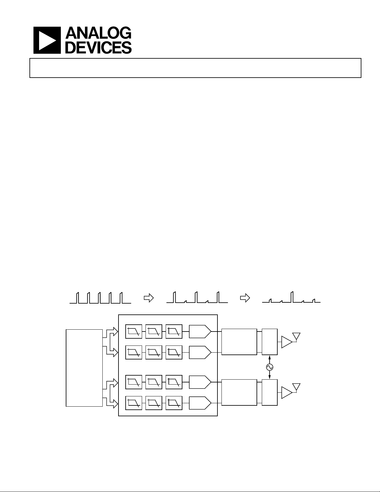
TYPICAL SIGNAL CHAIN
COMPLEX BASEBAND COMPLEX IF RF
TxDAC+ Digital-to-Analog Converter
AD9148
GENERAL DESCRIPTION
The AD9148 is a quad, 16-bit, high dynamic range, digital-toanalog converter (DAC) that provides a sample rate of 1000 MSPS.
This device includes features optimized for direct conversion
transmit applications, including gain, phase, and offset compensation. The DAC outputs are optimized to interface seamlessly with
analog quadrature modulators such as the ADL5371/ADL5372/
ADL5373/ADL5374/ADL5375. A serial peripheral interface (SPI)
is provided for programming of the internal device parameters.
Full-scale output current can be programmed over a range of 8.7 mA
to 31.7 mA. The device operates from 1.8 V and 3.3 V supplies
for a total power consumption of 3 W at the maximum sample
rate. The AD9148 is enclosed in a 196-ball chip scale package ball
grid array with the option of an attached heat spreader.
PRODUCT HIGHLIGHTS
1. Low noise and intermodulation distortion (IMD) enable
high quality synthesis of wideband signals from baseband
to high intermediate frequencies.
2. A proprietary DAC output switching technique enhances
dynamic performance.
3. The current outputs are easily configured for various
single-ended or differential circuit topologies.
4. The LVDS data input interface includes FIFO to ease input
timing.
DC
DIGITAL INTERPOL ATION F ILTERS
↑2 ↑2 ↑2
↑2 ↑2 ↑2
FPGA/ASI C/DSP
↑2 ↑2 ↑2
↑2 ↑2 ↑2
NOTES
1. AQM = ANALO G QUADRATURE MO DULATOR.
Rev. A
Information furnished by Analog Devices is believed to be accurate and reliable. However, no
responsibility is assumed by Analog Devices for its use, nor for any infringements of patents or other
rights of third parties that may result from its use. Specifications subject to change without notice. No
license is granted by implication or otherwise under any patent or patent rights of Analog Devices.
Trademarks and registered trademarks are the property of their respective owners.
LO ±
PA
PA
f
IF
f
IF
DAC1
POST DAC
ANALOG FI LTER
DAC2
DAC3
POST DAC
DAC4
Figure 1.
One Technology Way, P.O. Box 9106, Norwood, MA 02062-9106, U.S.A.
Tel: 781.329.4700 www.analog.com
Fax: 781.461.3113 ©2010–2011 Analog Devices, Inc. All rights reserved.
AQM
LO
LO
AQM
08910-001
Page 2

AD9148 Data Sheet
TABLE OF CONTENTS
Features.............................................................................................. 1
Applications....................................................................................... 1
General Description ......................................................................... 1
Product Highlights ........................................................................... 1
Typical Signal Chain......................................................................... 1
Revision History ............................................................................... 3
Functional Block Diagram .............................................................. 4
Specifications..................................................................................... 5
DC Specifications ......................................................................... 5
Input/Output Signal Specifications............................................ 6
Digital Input Data Timing Specifications ................................. 7
AC Specifications.......................................................................... 8
Absolute Maximum Ratings............................................................ 9
Thermal Resistance ...................................................................... 9
Maximum Safe Power Dissipation............................................. 9
ESD Caution.................................................................................. 9
Pin Configurations and Function Descriptions ......................... 11
Typical Performance Characteristics ........................................... 15
Terminology .................................................................................... 21
Serial Peripheral Interface ............................................................. 22
General Operation of the Serial Interface............................... 22
Data Format ................................................................................22
SPI Pin Descriptions ..................................................................22
SPI Options .................................................................................23
SPI Register Map............................................................................. 24
SPI Register Descriptions.......................................................... 26
Input Data Ports.............................................................................. 40
Dual-Port Mode.......................................................................... 40
Single-Port Mode........................................................................ 40
Byte Mode.................................................................................... 41
Data Interface Options ..............................................................41
Recommended Frame Input Bias Circuitry............................ 41
FIFO Operation ..............................................................................42
Synchronizing and Resetting the FIFO ................................... 43
Monitoring the FIFO Status...................................................... 44
Device Synchronization................................................................. 45
Synchronizing Multiple Devices .............................................. 45
Synchronization with Clock Multiplication............................... 45
Synchronization with Direct Clocking.................................... 47
Additional Synchronization Features ...................................... 48
Interface Timing............................................................................. 49
Digital Data Path ............................................................................ 50
Premodulation............................................................................ 50
Programmable Inverse Sinc Filter............................................ 50
Interpolation Filters ................................................................... 51
Fine Modulation......................................................................... 54
Quadrature Phase Correction................................................... 55
DC Offset Correction ................................................................ 55
Digital Gain Control.................................................................. 55
Clock Generation ........................................................................... 56
DAC Input Clock Configurations............................................ 56
Driving the CLK_x and REFCLK_x Inputs............................ 56
Direct Clocking .......................................................................... 56
Clock Multiplication.................................................................. 57
Analog Outputs............................................................................... 59
Transmit DAC Operation.......................................................... 59
Auxiliary DAC Operation......................................................... 60
Interfacing to Modulators ......................................................... 61
Device Power Dissipation.............................................................. 63
Temperature Sensor ....................................................................... 65
Interrupt Request Operation ........................................................ 66
Interrupt Service Routine.......................................................... 66
Interface Timing Validation.......................................................... 67
SED Operation............................................................................ 67
SED Example .............................................................................. 67
Example Start-Up Routine ............................................................ 68
Derived PLL Settings ................................................................. 68
Derived NCO Settings ............................................................... 68
Start-Up Sequence...................................................................... 68
Device Verification Sequence ................................................... 68
Outline Dimensions....................................................................... 69
Ordering Guide .......................................................................... 70
Rev. A | Page 2 of 72
Page 3

Data Sheet AD9148
REVISION HISTORY
9/11—Rev. 0 to Rev. A
Changes to General Description Section .......................................1
Deleted Input High Voltage, V
Low Voltage, V
or VIB Parameter, Table 2, and
IA
or VIB Parameter, Table 2, Input
IA
Note 2, Table 2; Renumbered Sequentially ....................................6
Added Input Voltage Range, V
or VIB Parameter, Table 2.........6
IA
Changes to Table 10 ........................................................................13
Changes to Figure 41 and Figure 42 .............................................23
Changes to 0x1E Addr, Table 12....................................................24
Deleted 0x74 Row, Table 12 ...........................................................26
Changes to PLL Control 2, Table 13 .............................................29
Changes to HB3 Control, 1E, Bit 7 Row, Table 13 ......................32
Deleted LVDS Pad Ctrl Row, Table 13..........................................38
Deleted Frame Input Levels Section and Table 15......................41
Added Recommended Frame Input Bias Circuitry Section and
Figure 45; Renumbered Sequentially............................................41
Changes to Timing Optimization Section...................................48
Added Table 15 ................................................................................ 48
Changes to Filter Implementation Section ..................................50
Changes to Figure 74 ......................................................................57
Deleted Test Access Port Section, Table 27, Figure 92, and
Table 28.............................................................................................68
Changes to Start-Up Sequence Section........................................ 68
Deleted Figure 93 ............................................................................69
Deleted Table 29 ..............................................................................70
6/10—Revision 0: Initial Version
Rev. A | Page 3 of 72
Page 4
AD9148 Data Sheet
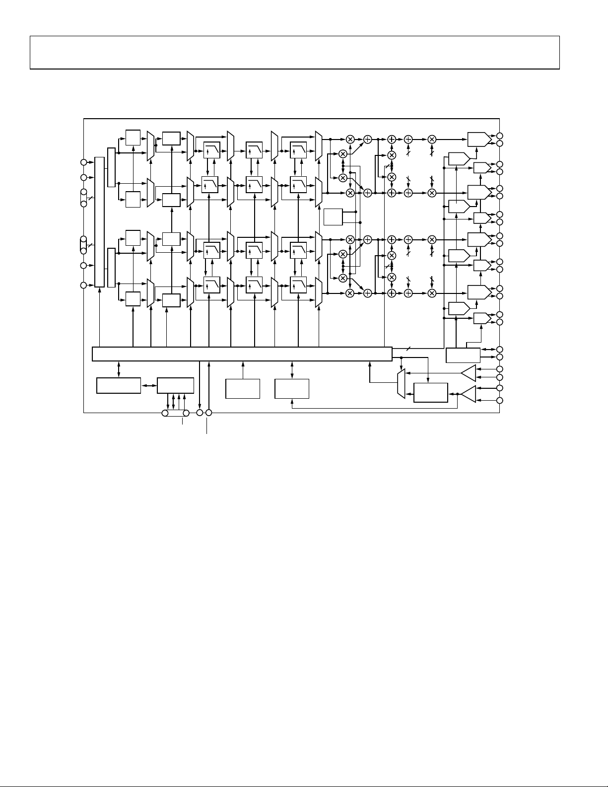
FUNCTIONAL BLOCK DIAGRAM
310MHz/620MHz 500MHz/1GHz 500MHz/1GHz
310MHz
–1
SINC
2× 2×
2× 2× 2×
–1
SINC
–1
SINC
2× 2×
2× 2×
–1
SINC
HB1_EN
HB1_CLK
INVSINE_EN
FILTER
COEFFI CIENT
INTERNA L CLOCK TIMING AND CON TRO L LOGI C
SERIAL
IN/OUT PORT
POWER-O N
RESET
1GHz
16-BIT
2×
COS
32-BIT
SIN
NCO
2×
2×
HB3_EN
HB3_CLK
HB2_EN
HB2_CLK
MULTI-CHIP
SYNC
SYNC
PHASE
CORRECTION
DAC_CLK
GAIN/
OFFSET_CTRL
PLL_CTRL
I OFFSET
Q OFFSET
I OFFSET
Q OFFSET
I GAIN
Q GAIN
I GAIN
Q GAIN
CLOCK
MULTIPLIER
(2× – 16×)
GAIN
16-BIT
GAIN
16-BIT
GAIN
16-BIT
GAIN
REFERENCE
BIAS
DAC1
DAC2
DAC3
DAC4
AUX1
AUX2
AUX3
AUX4
IOUT1_P
IOUT1_N
AUX1_P
AUX1_N
IOUT2_P
IOUT2_N
AUX2_P
AUX2_N
IOUT3_P
IOUT3_N
AUX3_P
AUX3_N
IOUT4_P
IOUT4_N
AUX4_P
AUX4_N
VREF
I120
CLK_P
CLK_N
REFCLK_P/
SYNC_P
REFCLK_N/
SYNC_N
DCIA_P/
DCIA_N
FRAMEA_P/
FRAMEA_N
A[15:0]_P/
A[15:0]_N
B[15:0]_P/
B[15:0]_N
FRAMEB_P/
FRAMEB_N
DCIB_P/
DCIB_N
1.2GHz
16
DATA RECEIVER
16
MODE
PROGRAMMING
REGISTERS
310MHz
f
/2
S
MOD
FIFO
f
/2
S
MOD
f
/2
S
MOD
FIFO
f
/2
S
MOD
PREMOD_EN
PREMOD_CLK
CS
SDO
IRQ
SDIO
SCLK
RESET
08910-002
Figure 2.
Rev. A | Page 4 of 72
Page 5

Data Sheet AD9148
SPECIFICATIONS
DC SPECIFICATIONS
T
to T
MIN
otherwise noted.
Table 1.
Parameter Min Typ Max Unit
RESOLUTION 16 Bits
ACCURACY
Differential Nonlinearity (DNL) ±2.1 LSB
Integral Nonlinearity (INL) ±3.7 LSB
MAIN DAC OUTPUTS
Offset Error ±0.001 % FSR
Gain Error (with Internal Reference) ±2 % FSR
Full-Scale Output Current1 8.66 20.2 31.66 mA
Output Compliance Range −1.0 +1.0 V
Output Resistance 10 MΩ
Gain DAC Monotonicity Guaranteed
Settling Time to Within ±0.5 LSB 20 ns
TEMPERATURE DRIFT
Main DAC Offset 0.04 ppm/°C
Main DAC Gain 100 ppm/°C
Reference Voltage 30 ppm/°C
REFERENCE
Internal Reference Voltage 1.2 V
Output Resistance 5 kΩ
ANALOG SUPPLY VOLTAGES
AVDD33 3.13 3.3 3.47 V
CVDD18 1.71 1.8 1.89 V
DIGITAL SUPPLY VOLTAGES
IOVDD 1.71 1.8/3.3 3.47 V
DVDD18 1.71 1.8 1.89 V
POWER CONSUMPTION (NCO OFF, PLL DISABLED, AND SINC−1 FILTER BYPASSED,
UNLESS OTHERWISE NOTED)
1 × Mode, f
2 × Mode, f
4 × Mode, f
4 × Mode, f
4 × Mode, f
4 × Mode, f
8 × Mode, f
Power-Down Mode 1 12 mW
OPERATING RANGE −40 +25 +85 °C
1
Based on a 10 k external resistor.
, AVDD33 = 3.3 V, IOVDD = 3.3 V, DVDD18 = 1.8 V, CVDD18 = 1.8 V, I
MAX
= 20 mA, maximum sample rate, unless
OUTFS
= 300 MSPS, f
DAC
= 500 MSPS, f
DAC
= 800 MSPS, f
DAC
= 800 MSPS, f
DAC
= 800 MSPS, f
DAC
= 800 MSPS, f
DAC
= 800 MSPS, f
DAC
= 600 MSPS 0.79 W
INTERFACE
= 500 MSPS 1.49 W
INTERFACE
= 400 MSPS 2.18 W
INTERFACE
= 400 MSPS, NCO On 2.47 W
INTERFACE
= 400 MSPS, PLL Enabled 2.26 W
INTERFACE
= 400 MSPS, Sinc−1 Filter Enabled 2.44 W
INTERFACE
= 200 MSPS 2.01 2.16 W
INTERFACE
AVDD33 368 373 mW
CVDD18 261 280 mW
IOVDD 0.8 1.6 mW
DVDD18 1377 1504 mW
Rev. A | Page 5 of 72
Page 6

AD9148 Data Sheet
INPUT/OUTPUT SIGNAL SPECIFICATIONS
T
to T
MIN
otherwise noted. LVDS driver and receiver are compliant to the IEEE-1596 reduced range link, unless otherwise noted.
Table 2.
Parameter Min Typ Max Unit
CMOS INPUT LOGIC LEVEL (SCLK, SDIO, CS, RESET, TMS, TDI, TCK)
Input VIN Logic High (IOVDD = 1.8 V) 1.2 V
Input VIN Logic High (IOVDD = 3.3 V) 2.0 V
Input VIN Logic Low (IOVDD = 1.8 V) 0.6 V
Input VIN Logic Low (IOVDD = 3.3 V) 0.8 V
CMOS OUTPUT LOGIC LEVEL (SDIO, SDO, IRQ, PLL_LOCK, TDO)
Output V
Output V
Output V
Output V
LVDS RECEIVER INPUTS (A[15:0]_x, B[15:0]_x, DCIA_x, DCIB_x)
Input Voltage Range, VIA or VIB 825 1575 mV
Input Differential Threshold, V
Input Differential Hysteresis, V
Receiver Differential Input Impedance, RIN 80 120 Ω
LVDS Input Rate, f
LVDS RECEIVER INPUTS (FRAMEA_x, FRAMEB_x)
Input Voltage Range, VIA or VIB 825 1575 mV
DAC CLOCK INPUT (CLK_P, CLK_N)
Differential Peak-to-Peak Voltage 100 500 2000 mV
Common-Mode Voltage (Self-Biasing, AC-Coupled) 1.25 V
Maximum Clock Rate 1000 MSPS
REFERENCE CLOCK INPUT (REFCLK_x/SYNC_x)
Differential Peak-to-Peak Voltage 100 500 2000 mV
Common-Mode Voltage (Self-Biasing, AC-Coupled) 1.25 V
Maximum Clock Rate 500 MSPS
Minimum Clock Rate (PLL Enabled)
SERIAL PERIPHERAL INTERFACE
Maximum Clock Rate (SCLK) 40 MHz
Minimum Pulse Width High (t
Minimum Pulse Width Low (t
Set-Up Time, SDI to SCLK (tDS) 1.9 ns
Hold Time, SDI to SCLK (tDH) 0.2 ns
Data Valid, SDO to SCLK (tDV) 23 ns
Setup time, CS to SCLK (t
, AVDD33 = 3.3 V, IOVDD = 3.3 V, DVDD18 = 1.8 V, CVDD18 = 1.8 V, I
MAX
= 20 mA, maximum sample rate, unless
OUTFS
Logic High (IOVDD = 1.8 V) 1.4 V
OUT
Logic High (IOVDD = 3.3 V) 2.4 V
OUT
Logic Low (IOVDD = 1.8 V) 0.4 V
OUT
Logic Low (IOVDD = 3.3 V) 0.4 V
OUT
−100 +100 mV
IDTH
to V
IDTHH
(See Table 4) 1200 MSPS
INTERFACE
20 mV
IDTHL
Loop Divider = /2 125 MSPS
Loop Divider = /4 62.5 MSPS
Loop Divider = /8 31.25 MSPS
Loop Divider = /16 15.625 MSPS
) 12.5 ns
PWH
) 12.5 ns
PWL
DCSB
)
1.4 ns
Rev. A | Page 6 of 72
Page 7
Data Sheet AD9148
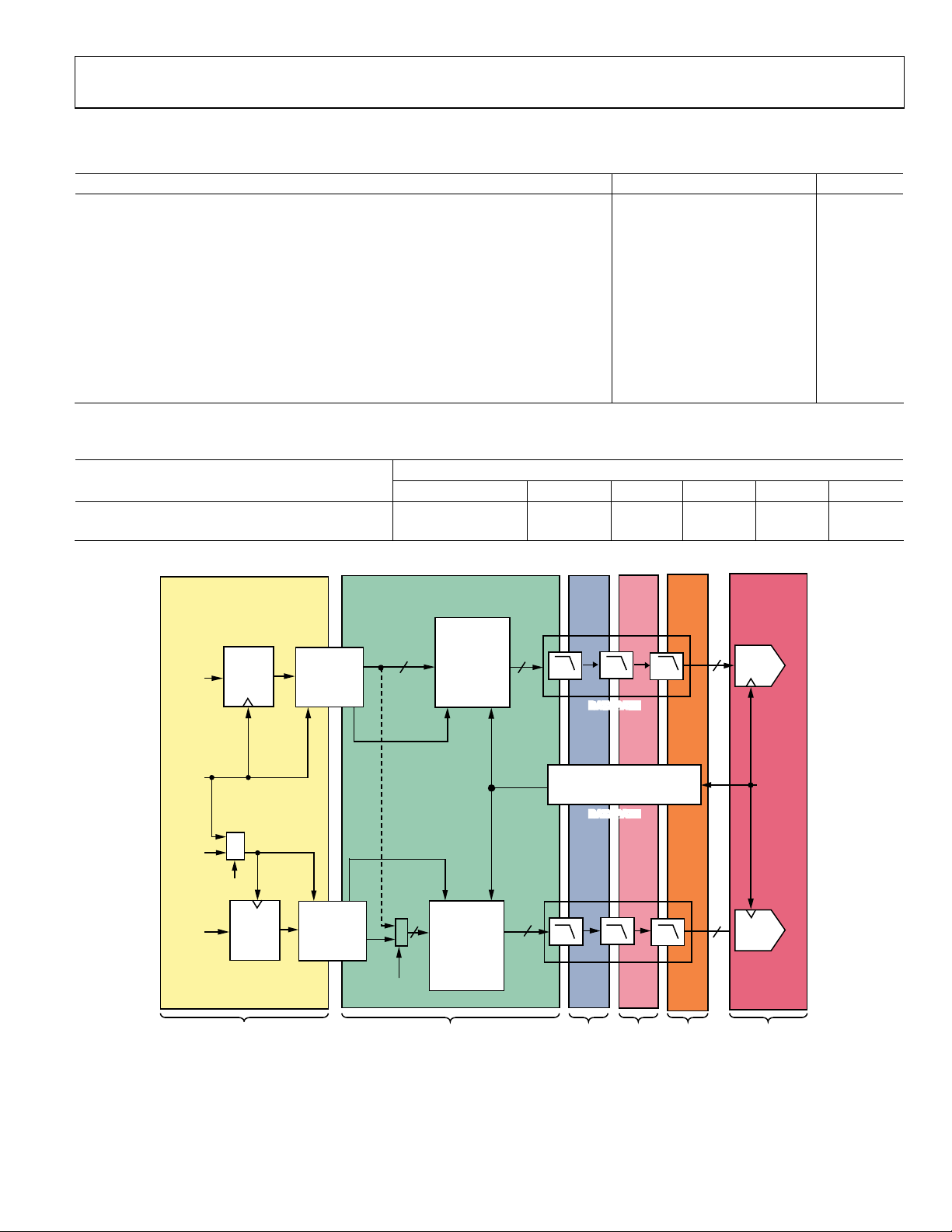
DIGITAL INPUT DATA TIMING SPECIFICATIONS
Table 3.
Parameter Min Typ Max Unit
LATENCY (DACCLK CYCLES)
1× Interpolation (with or Without Coarse Modulation) 64 Cycles
2× Interpolation (with or Without Coarse Modulation) 125 Cycles
4× Interpolation (with or Without Coarse Modulation) 254 Cycles
8× Interpolation (with or Without Coarse Modulation) 508 Cycles
Inverse Sinc (1× Interpolation) 10 Cycles
Inverse Sinc (2× Interpolation) 20 Cycles
Inverse Sinc (4× Interpolation) 40 Cycles
Inverse Sinc (8× Interpolation) 80 Cycles
Fine Modulation 12 Cycles
Power–Up Time 100 ms
Table 4. Maximum Rate
Interface Mode f
f
INTERFACE
Dual Port Mode 620 310 620 1000 1000 1000
Single Port Mode or Byte Mode 1200 300 600 1000 1000 1000
Maximum Rate (MSPS)
f
DATA
HB1
f
f
HB2
f
HB3
DAC
DAC1
DATA
PORT A
DCIA
DCIB
DATA
PORT B
INPUT
LATCH
ONE DCI
INPUT
LATCH
f
INTERFACE
DATA
ASSEMBLER
DATA
ASSEMBLER
32
WRITE PTR A
WRITE PTR B
32 32
INTERFACE
MODE
f
DATA
FIFO A
FIFO B
32
2×
A
R
T
P
D
A
E
R
B
R
T
P
D
A
E
R
2×
2×
DATAPATH
CLK GENERATOR
AND DISTRIBUTO R
DATAPATH
2×
f
HB1
f
HB2
2×
2×
32
AND
DAC2
DACCLK
32
DAC3
AND
DAC4
f
HB3
f
DAC
08910-003
Figure 3. Defining Maximum Rates
Rev. A | Page 7 of 72
Page 8

AD9148 Data Sheet
AC SPECIFICATIONS
T
to T
MIN
otherwise noted.
Table 5.
Parameter Min Typ Max Unit
SPURIOUS-FREE DYNAMIC RANGE (SFDR)
f
DAC
f
DAC
f
DAC
TWO-TONE INTERMODULATION DISTORTION (IMD)
f
DAC
f
DAC
f
DAC
NOISE SPECTRAL DENSITY (NSD) EIGHT-TONE, 500 kHz TONE SPACING
f
DAC
f
DAC
f
DAC
W-CDMA ADJACENT CHANNEL LEAKAGE RATIO (ACLR), SINGLE CARRIER
f
DAC
f
DAC
f
DAC
f
DAC
W-CDMA ALTERNATE CHANNEL LEAKAGE RATIO, SINGLE CARRIER
f
DAC
f
DAC
f
DAC
f
DAC
, AVDD33 = 3.3 V, IOVDD = 3.3 V, DVDD18 = 1.8 V, CVDD18 = 1.8 V, I
MAX
= 400 MSPS, f
= 600 MSPS, f
= 1000 MSPS, f
= 400 MSPS, f
= 600 MSPS, f
= 1000 MSPS, f
= 200 MSPS, f
= 400 MSPS, f
= 800 MSPS, f
= 737.28 MSPS, f
= 737.28 MSPS, f
= 737.28 MSPS, f
= 737.28 MSPS, f
= 737.28 MSPS, f
= 737.28 MSPS, f
= 737.28 MSPS, f
= 737.28 MSPS, f
= 80 MHz 72 dBc
OUT
= 100 MHz 67 dBc
OUT
= 100 MHz 65 dBc
OUT
= 100 MHz 85 dBc
OUT
= 120 MHz 82 dBc
OUT
= 150 MHz 76 dBc
OUT
= 80 MHz −160 dBm/Hz
OUT
= 100 MHz −161 dBm/Hz
OUT
= 100 MHz −162.5 dBm/Hz
OUT
= 100 MHz, PLL Off −81 dBc
OUT
= 100 MHz, PLL On −78 dBc
OUT
= 200 MHz, PLL Off −79 dBc
OUT
= 200 MHz, PLL On −72.5 dBc
OUT
= 100 MHz, PLL Off −87 dBc
OUT
= 100 MHz, PLL On −83 dBc
OUT
= 200 MHz, PLL Off −84 dBc
OUT
= 200 MHz, PLL On −80.5 dBc
OUT
= 20 mA, maximum sample rate, unless
OUTFS
Rev. A | Page 8 of 72
Page 9
Data Sheet AD9148
(
)
(
)
ABSOLUTE MAXIMUM RATINGS
Table 7. Thermal Resistance Table 6.
With
Parameter
AVDD33, IOVDD
DVDD18, CVDD18
AGND
DGND
CGND
I120, VREF AGND −0.3 V to AVDD33 + 0.3 V
IOUT1_P, IOUT1_N,
IOUT2_P, IOUT2_N,
IOUT3_P, IOUT3_N,
IOUT4_P, IOUT4_N
A15_P to A0_P,
A15_N to A0_N,
B15_P to B0_P,
B15_N, B0_N
DCIA_P, DCIA_N,
FRAMEA_P, FRAMEA_N,
DCIB_P, DCIB_N,
FRAMEB_P, FRAMEB_N
CLK_P, CLK_N,
REFCLK_P, REFCLK_N
CSB, SCLK, SDIO, SDO,
TDO, TDI, TCK, TMS,
RESET, IRQ, PLL_LOCK
Junction Temperature 125°C
Storage Temperature
Range
Respect To Ratin g
AGND,
DGND,
CGND
AGND,
DGND,
CGND
DGND,
CGND
AGND,
CGND
AGND,
DGND
AGND −1.0 V to AVDD33 + 0.3 V
DGND −0.3 V to DVDD18 + 0.3 V
DGND −0.3 V to DVDD18+ 0.3 V
CGND −0.3 V to CVDD18 + 0.3 V
DGND −0.3 V to IOVDD + 0.3 V
−65°C to +150°C
−0.3 V to +3.6 V
−0.3 V to +2.10 V
−0.3 V to +0.3 V
−0.3 V to +0.3 V
−0.3 V to +0.3 V
Stresses above those listed under Absolute Maximum Ratings
may cause permanent damage to the device. This is a stress
rating only; functional operation of the device at these or any
other conditions above those indicated in the operational
section of this specification is not implied. Exposure to absolute
maximum rating conditions for extended periods may affect
device reliability.
THERMAL RESISTANCE
Typical θJA, θJB, and θJC are specified vs. the number of PCB layers in
still air for each package offering. Airflow increases heat dissipation
effectively reducing θ
and θJB.
JA
Rev. A | Page 9 of 72
Package Type θ
196-Ball CSP_BGA 24.7 12.6 5.7 °C/W
19.2 10.9 5.3 °C/W
18.1 10.5 5.3 °C/W
18.0 10.5 5.3 °C/W
196-Ball BGA_ED 20.9 8.6 3.1 °C/W
16.2 7.7 3.1 °C/W
15.2 7.4 3.1 °C/W
15.0 7.4 3.1 °C/W
MAXIMUM SAFE POWER DISSIPATION
The maximum junction temperature for the AD9148 is 125°C.
With the thermal resistance of the molded package (CSP_BGA)
given for a 12 layer board, the maximum power that can be
dissipated in this package can be calculated as
Power
=
MAX
To increase the maximum power, the AD9148 is available in a
second package option (BGA_ED), which includes a heat spreader
on top of the package. Also, an external heat sink can be attached to
the top of the AD9148 CSP_BGA package. The adjusted maximum
power for each of these conditions is shown in Tab le 8.
With the thermal resistance of the heat spreader package (BGA_ED)
given for a 12-layer board, the maximum power that can be
dissipated in this package can be calculated as
Power
=
MAX
To increase the maximum power, an external heat sink can be
attached to the top of the AD9148 BGA_ED package. The adjusted
maximum power for an external heat sink is shown in Tabl e 8.
To aid in the selection of package, the maximum f
power dissipation over several operating conditions is shown in
Tabl e 9. The maximum f
Note that, if the programmable inverse sinc filter is enabled, the
maximum f
rate specified in Ta b le 9 decreases.
DAC
ESD CAUTION
θ
JA
JB θJC
−
TT
J
θ
−
J
θ
()
A
=
JA
TT
()
A
=
JA
rate applies to all interpolation rates.
DAC
Unit Notes
85125=−
0.18
85125=−
0.15
W
22.2
W
67.2
DAC
4-layer board,
25 PCB vias
8-layer board,
25 PCB vias
10-layer board,
25 PCB vias
12-layer board,
25 PCB vias
4-layer board,
25 PCB vias
8-layer board,
25 PCB vias
10-layer board,
25 PCB vias
12-layer board,
25 PCB vias
rate for a given
Page 10
AD9148 Data Sheet
Table 8. Thermal Resistance and Maximum Power
PCB
Package Type TA (°C) PCB Layers PCB Vias External Heat Sink1 Case TJ (°C) θJA (°C/W)
196-ball CSP_BGA 85 12 25 No CSP_BGA 125 18.0 2.22
196-ball CSP_BGA 85 12 25 Yes CSP_BGA 125 16.0 2.50
196-ball BGA_ED 85 12 25 No BGA_ED 125 15.0 2.67
196-ball BGA_ED 85 12 25 Yes BGA_ED 125 14.0 2.86
1
Heat sink is used in the thermal model: 13 mm × 13 mm, 15 mm tall.
Maximum
Power (W)
Table 9. Power vs. f
Rate and Functionality
DAC
Maximum f
(MSPS)1
DAC
Coarse Modulation Fine Modulation (NCO)
Maximum Power (W) Package Heat-Sink Combination2 PLL Off PLL On PLL Off PLL On
2.22 CSP_BGA No 820 740 695 630
2.50 CSP_BGA Yes 950 875 810 740
2.67 BGA_EP No 1000 945 870 810
2.86 BGA_EP Yes 1000 1000 940 870
1
Typical maximum f
2
Heat sink is used in the thermal model: 13 mm × 13 mm, 15 mm tall.
rate with inverse sinc filter off.
DAC
Rev. A | Page 10 of 72
Page 11
Data Sheet AD9148
PIN CONFIGURATIONS AND FUNCTION DESCRIPTIONS
23
1
A
4
IOUT2 IOUT2
5
67
V
CLK
REF
I120
8
REF
12 13
IOUT3 IOUT3
10 11
9
14
A
NC
+
X
AVSS
NC REF
+
+
XX
9
8
AUX3 AUX3
X
10 11
POSITIVE
TERMINAL
CLKCLK
AUX4
12 13
NEGATIVE
TERMINAL
IOUT4AUX4
IOUT4
14
B
C
D
E
F
G
H
J
K
L
M
N
P
08910-004
AUX1
AUX1
23
CVDD18
+
AUX2 AUX2
4
X
B
IOUT1
C
IOUT1
D
E
F
G
H
J
K
L
M
N
P
1
XX
5
AVDD33
CLK
+
67
Figure 4. Pin Configuration (Top View), Analog and Clock Domain Pins
Rev. A | Page 11 of 72
Page 12
AD9148 Data Sheet
A
B
C
D
E
F
SPI
INTERFACE
G
H
J
K
L
M
N
23
1
CSSDO
SCLK
SDIO
FrB
DCIB DCIA
DCIB
A0
A2
A0 A2
A3
RESET IRQ
B0 B2
B0 B2
B1
B1
4
++
B3
B3 B4B4B5
A5 A6A6A7
67
5
XXXXXX
XXXXXX
B5 B6B6B7
8
B7 B8 B9 B10
A8 A9 A10 A11 A12 A1 3 A1 4 A15A1
10 11
9
B8 B9 B10
Trch Trc h
B11
B11
12 13
TMS
TDONC PLL
TCK
B13
B13
B12 B14 B15
B12 B14 B15
DCIA
FrA
FrAFrB
14
A
B
C
D
E
F
TAP
INTERFACE
TDI
G
H
J
K
L
M
N
P
A1
1
+
A4A4A5
A3
23
IOVDD
X
4
5
DVDD18
A7 A8 A9 A10 A 11 A12 A13 A14 A15
67
DVSS
8
10 11
9
+LVDS –LVDS
A15A15
12 13
Figure 5. Pin Configuration (Top View), Digital Domain Pins
Table 10. Pin Function Description
Pin No. Mnemonic Description
E6, E7, E8, E9 CVDD18 1.8 V Clock Supply.
F5, F6, F7, F8, F9, F10 AVDD33 3.3 V Analog Supply.
A1, A2, A5, A10, A13, A14, B1,
AVSS Analog Supply Ground.
B2, B5, B10, B13, B14, C3, C4, C5,
C6, C7, C8, C9, C10, C11, C12, D3,
D4, D5, D6, D7, D8, D9, D10, D11,
D12, E1, E2, E3, E4, E5, E10, E11,
E12, E13, E14, F1, F2, F3, F4, F11,
F12, F13, F14
G5, G6, G7, G8, G9, G10, H5, H6,
DVSS Digital Supply Ground.
H7, H8, H9, H10
G3, G4 IOVDD
Supply for Serial Ports (SPI and TAP), RESET
supplied to these pins.
J5, J6, J7, J8, J9, J10, K5, K6, K7,
DVDD18 1.8 V Digital Supply.
K8, K9, K10
B7, B8, H11 NC No Connect. Do not connect to this pin.
C1 IOUT1_N DAC 1 Complementary Output Current.
D1 IOUT1_P DAC 1 Positive Output Current.
A3 IOUT2_N DAC 2 Complementary Output Current.
A4 IOUT2_P DAC 2 Positive Output Current.
A11 IOUT3_P DAC 3 Positive Output Current.
A12 IOUT3_N DAC 3 Complementary Output Current.
Rev. A | Page 12 of 72
P
14
08910-005
and IRQ. 1.8 V to 3.3 V can be
Page 13

Data Sheet AD9148
Pin No. Mnemonic Description
C14 IOUT4_N DAC 4 Complementary Output Current.
D14 IOUT4_P DAC 4 Positive Output Current.
C2 AUX1_N Auxiliary DAC 1 Complementary Output Current.
D2 AUX1_P Auxiliary DAC 1 Positive Output Current.
B3 AUX2_N Auxiliary DAC 2 Complementary Output Current.
B4 AUX2_P Auxiliary DAC 2 Positive Output Current.
B11 AUX3_P Auxiliary DAC 3 Positive Output Current.
B12 AUX3_N Auxiliary DAC 3 Complementary Output Current.
C13 AUX4_N Auxiliary DAC 4 Complementary Output Current.
D13 AUX4_P Auxiliary DAC 4 Positive Output Current.
A8 I120 Tie to analog ground via a 10 kΩ resistor to generate a 120 μA reference current.
A7 VREF
B6, A6 CLK_P/CLK_N Positive/Negative DAC Clock Input (CLK).
B9, A9
H4
H3
G1 SDO Serial Data Output for SPI.
G2
H1 SDIO Serial Data Input/Output for SPI.
H2 SCLK Qualifying Clock Input for SPI.
G11, G12 TRENCH Connect this pin to VSS.
H12 PLL_LOCK Active High LVCMOS Output. It indicates the lock status of the PLL circuitry.
G13 TMS Reserved for Future Use. Connect to DVSS.
G14 TDI Reserved for Future Use. Connect to DVSS.
H13 TCK Reserved for Future Use. Connect to DVSS.
H14 TDO Reserved for Future Use. Leave unconnected.
M1, L1 A0_P/A0_N LVDS Data Input Pair, Port A (LSB).
P1, N1 A1_P/A1_N LVDS Data Input Pair, Port A.
M2, L2 A2_P/A2_N LVDS Data Input Pair, Port A.
P2, N2 A3_P/A3_N LVDS Data Input Pair, Port A.
P3, N3 A4_P/A4_N LVDS Data Input Pair, Port A.
P4, N4 A5_P/A5_N LVDS Data Input Pair, Port A.
P5, N5 A6_P/A6_N LVDS Data Input Pair, Port A.
P6, N6 A7_P/A7_N LVDS Data Input Pair, Port A.
P7, N7 A8_P/A8_N LVDS Data Input Pair, Port A.
P8, N8 A9_P/A9_N LVDS Data Input Pair, Port A.
P9, N9 A10_P/A10_N LVDS Data Input Pair, Port A.
P10, N10 A11_P/A11_N LVDS Data Input Pair, Port A.
P11, N11 A12_P/A12_N LVDS Data Input Pair, Port A.
P12, N12 A13_P/A13_N LVDS Data Input Pair, Port A.
P13, N13 A14_P/A14_N LVDS Data Input Pair, Port A.
P14, N14 A15_P/A15_N LVDS Data Input Pair, Port A (MSB).
K13, J13 DCIA_P/DCIA_N LVDS Data Clock Input Pair for Port A.
K14, J14 FRAMEA_P/FRAMEA_N
K3, J3 B0_P/B0_N LVDS Data Input Pair, Port B (LSB).
M3, L3 B1_P/B1_N LVDS Data Input Pair, Port B.
K4, J4 B2_P/B2_N LVDS Data Input Pair, Port B.
M4, L4 B3_P/B3_N LVDS Data Input Pair, Port B.
M5, L5 B4_P/B4_N LVDS Data Input Pair, Port B
M6, L6 B5_P/B5_N LVDS Data Input Pair, Port B.
REFCLK_P/REFCLK_N or
SYNC_P/SYNC_N
Active Low Open-Drain Interrupt Request Output. Pull up to IOVDD with
IRQ
RESET
CS
Band Gap Voltage Reference I/O. Decouple to analog ground via a 0.1 μF
capacitor. Output impedance is approximately 5 kΩ.
PLL Reference Clock Input (REFCLK_x). This pin has a secondary function as
a synchronization input (SYNC_x).
a 10 kΩ resistor.
An active low LVCMOS input resets the device. Pull up to IOVDD.
Active Low Chip Select for SPI.
LVDS Frame Input for Port A. Tie to LVDS logic low if not used.
Recommended external bias circuit is shown in Figure 49.
Rev. A | Page 13 of 72
Page 14

AD9148 Data Sheet
Pin No. Mnemonic Description
M7, L7 B6_P/B6_N LVDS Data Input Pair, Port B.
M8, L8 B7_P/B7_N LVDS Data Input Pair, Port B.
M9, L9 B8_P/B8_N LVDS Data Input Pair, Port B.
M10, L10 B9_P/B9_N LVDS Data Input Pair, Port B.
M11, L11 B10_P/B10_N LVDS Data Input Pair, Port B.
K11, J11 B11_P/B11_N LVDS Data Input Pair, Port B.
M12, L12 B12_P/B12_N LVDS Data Input Pair, Port B.
K12, J12 B13_P/B13_N LVDS Data Input Pair, Port B.
M13, L13 B14_P/B14_N LVDS Data Input Pair, Port B.
M14, L14 B15_P/B15_N LVDS Data Input Pair, Port B (MSB).
K2, J2 DCIB_P/DCIB_N LVDS Data Clock Input Pair for Port B.
K1, J1 FRAMEB_P/FRAMEB_N
LVDS Frame Input for Port B. Tie to LVDS logic low if not used.
Recommended external bias circuit is shown in Figure 49.
Rev. A | Page 14 of 72
Page 15
Data Sheet AD9148
–
–
–
–
–
–
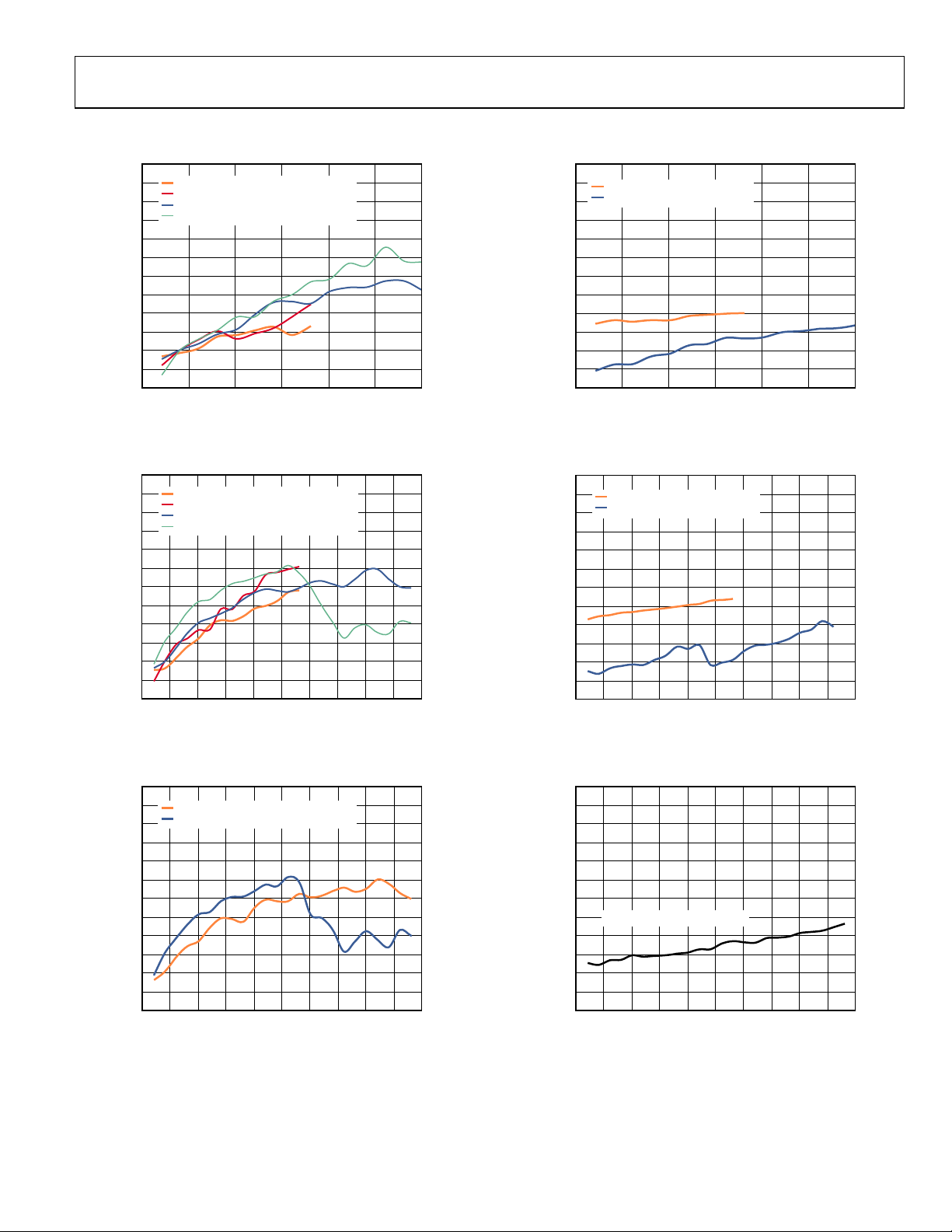
TYPICAL PERFORMANCE CHARACTERISTICS
30
–35
–40
–45
–50
–55
–60
–65
–70
HARMONIC LEVE L (dBc)
–75
–80
–85
–90
Figure 6. Harmonic Level vs. f
f
= 200MSPS, SE COND HARMONIC
DATA
f
= 200MSPS, T HIRD HARMONIC
DATA
f
= 310MSPS, SE COND HARMONIC
DATA
f
= 310MSPS, T HIRD HARMONIC
DATA
0 50 100 150 200 250 300
f
OUT
OUT
(MHz)
over f
, 2× Interpolation,
DATA
Digital Scale = 0 dBFS, Full-Scale Current = 20 mA
30
–35
–40
–45
–50
–55
–60
–65
–70
HARMONIC LEVE L (dBc)
–75
–80
–85
–90
Figure 7. Harmonic Level vs. f
f
= 150MSPS, SE COND HARMONIC
DATA
f
= 150MSPS, T HIRD HARMONIC
DATA
f
= 250MSPS, SE COND HARMONIC
DATA
f
= 250MSPS, T HIRD HARMONIC
DATA
0 50 100 150 200 250 300 350 400 450 500
f
OUT
OUT
(MHz)
over f
, 4× Interpolation,
DATA
Digital Scale = 0 dBFS, Full-Scale Current = 20 mA
30
–35
–40
–45
–50
–55
–60
–65
–70
HARMONIC LEVE L (dBc)
–75
–80
–85
–90
Figure 8. Harmonic Level vs. f
f
= 125MSPS, SE COND HARMONIC
DATA
f
= 125MSPS, T HIRD HARMONIC
DATA
0 50 100 150 200 250 300 350 400 450 500
f
(MHz)
OUT
, 8× Interpolation over f
OUT
Digital Scale = 0 dBFS, Full-Scale Current = 20 mA
= 125 MSPS,
DATA
08910-006
08910-007
08910-008
30
–35
–40
–45
–50
–55
–60
–65
–70
SPUR LEVEL (dBc)
–75
–80
–85
–90
Figure 9. Highest Digital Spur vs. f
f
= 200MSPS,
DATA
f
= 310MSPS,
DATA
0 50 100 150 200 250 300
f
DATA
f
DATA
f
OUT
+
f
OUT
+
f
OUT
(MHz)
OUT
over f
DATA
Digital Scale = 0 dBFS, Full-Scale Current = 20 mA
30
–35
–40
–45
–50
–55
–60
–65
–70
SPUR LEVEL (dBc)
–75
–80
–85
–90
Figure 10. Highest Digital Spur vs. f
f
= 150MSPS,
DATA
f
= 250MSPS, 2
DATA
0 50 100 150 200 250 300 350 400 450 500
f
DATA
f
f
OUT
DATA
+
f
–
(MHz)
OUT
OUT
f
OUT
over f
DATA
Digital Scale = 0 dBFS, Full-Scale Current = 20 mA
30
–35
–40
–45
–50
–55
–60
–65
–70
SPUR LEVEL (dBc)
–75
–80
–85
–90
Figure 11. Highest Digital Spur vs. f
f
= 125MSPS,
DATA
0 50 100 150 200 250 300 350 400 450 500
f
+
f
DATA
OUT
f
(MHz)
OUT
, 8× Interpolation, f
OUT
Digital Scale = 0 dBFS, Full-Scale Current = 20 mA
, 2× Interpolation,
, 4× Interpolation,
= 125 MSPS,
DATA
08910-009
08910-010
08910-011
Rev. A | Page 15 of 72
Page 16
AD9148 Data Sheet
–
–
–
30
–35
–40
–45
–50
–55
–60
–65
–70
HARMONIC LEVE L (dBc)
–75
–80
–85
–90
Full-Scale Current = 20 mA, 4× Interpolation, f
–35
–40
–45
–50
–55
–60
–65
–70
HARMONIC LEVE L (dBc)
–75
–80
–85
–90
–10
–20
–30
–40
–50
–60
POWER LEVEL (dBm)
–70
–80
–90
Figure 14. 4× Interpolation, f
0dBFS, SE COND HARMONIC
–6dBFS, SECOND HARMONIC
–12dBFS, SECOND HARMONIC
–18dBFS, SECOND HARMONIC
0 50 100 150 200 250 300
Figure 12. Second Harmonic vs. f
30
10mA, SECOND HARMONIC
10mA, THIRD HARMONI C
20mA, SECOND HARMONI C
20mA, THIRD HARMONI C
30mA, SECOND HARMONI C
30mA, THIRD HARMONI C
0 50 100 150 200 250 300
Figure 13. Second Harmonic vs. f
Digital Scale = 0 dBFS, 4× Interpolation, f
0
0 100 200 300 400 500 600
f
(MHz)
OUT
OUT
f
(MHz)
OUT
over Full-Scale Current,
OUT
FREQUENCY ( MHz)
= 150 MSPS, f
DATA
over Digital Scale,
DATA
= 150 MSPS
DATA
OUT
= 150 MSPS
= 131 MHz
08910-012
08910-013
08910-014
30
–35
–40
–45
–50
–55
–60
–65
–70
HARMONIC LEVE L (dBc)
–75
–80
–85
–90
Full-Scale Current = 20 mA, 4× Interpolation, f
–10
–20
–30
–40
–50
–60
POWER LEVEL (dBm)
–70
–80
–90
Figure 16. 2× Interpolation, f
0dBFS, T HIRD HARMONIC
–6dBFS, T HIRD HARMONIC
–12dBFS, T HIRD HARMONIC
–18dBFS, T HIRD HARMONIC
0 50 100 150 200 250 300
Figure 15. Third Harmonic vs. f
0
0 100 200 300 400 500 600
f
(MHz)
OUT
over Digital Scale,
OUT
FREQUENCY ( MHz)
= 310 MSPS, f
DATA
DATA
OUT
0
–10
–20
–30
–40
–50
–60
POWER LEVEL (dBm)
–70
–80
–90
0 100 200 30 0 400 500 600 700 800 900 1000
Figure 17. 8× Interpolation, f
FREQUENCY ( MHz)
= 125 MSPS, f
DATA
OUT
= 150 MSPS
= 131 MHz
= 131 MHz
08910-015
08910-016
08910-017
Rev. A | Page 16 of 72
Page 17
Data Sheet AD9148
–
–
–
–
–
–
30
–35
–40
–45
IMD (dBc)
–50
–55
–60
–65
–70
–75
–80
–85
–90
–95
–100
f
= 200MSPS
DATA
f
= 310MSPS
DATA
0 50 100 150 200 250 300 350
Figure 18. IMD vs. f
OUT
f
OUT
over f
(MHz)
, 2× Interpolation,
DATA
Digital Scale = 0 dBFS, Full-Scale Current = 20 mA
30
–35
–40
–45
–50
–55
–60
–65
f
= 125MSPS
DATA
–70
IMD (dBc)
–75
–80
–85
–90
–95
–100
0 50 100 150 200 250 300 350 400 450 500
Figure 19. IMD vs. f
f
(MHz)
OUT
, 8× Interpolation, f
OUT
= 125 MSPS,
DATA
Digital Scale = 0 dBFS, Full-Scale Current = 20 mA
30
–35
IMD (dBc)
–40
–45
–50
–55
–60
–65
–70
–75
–80
–85
–90
–95
–100
0dBFS
–6dBFS
–12dBFS
–18dBFS
0 50 100 150 200 250 300
Figure 20. IMD vs. f
f
= 150 MSPS, Full-Scale Current = 20 mA
DATA
f
(MHz)
OUT
over Digital Scale, 4× Interpolation,
OUT
08910-018
08910-019
08910-020
30
–35
–40
–45
IMD (dBc)
–50
–55
–60
–65
–70
–75
–80
–85
–90
–95
–100
f
= 150MSPS
DATA
f
= 250MSPS
DATA
0 50 100 150 200 250 300 350 400 450 500
Figure 21. IMD vs. f
OUT
f
OUT
over f
(MHz)
DATA
, 4× Interpolation,
Digital Scale = 0 dBFS, Full-Scale Current = 20 mA
30
–35
–40
–45
–50
–55
–60
–65
–70
IMD (dBc)
–75
–80
–85
–90
–95
–100
4× Interpolation, f
30
–35
–40
–45
–50
–55
–60
–65
–70
IMD (dBc)
–75
–80
–85
–90
–95
–100
10mA
20mA
30mA
0 50 100 150 200 250 300
Figure 22. IMD vs. f
PLL OFF
PLL ON
0 50 100 150 200 250 300
Figure 23. IMD vs. f
f
(MHz)
OUT
over Full-Scale Current,
OUT
= 150 MSPS, Digital Scale = 0 dBFS
DATA
f
(MHz)
OUT
, PLL On and Off,
OUT
Digital Scale = 0 dBFS, Full-Scale Current = 20 mA
08910-021
08910-022
08910-023
Rev. A | Page 17 of 72
Page 18
AD9148 Data Sheet
–
–
–
–
–
–
144
–146
–148
–150
–152
–154
–156
NSD (dBm/Hz)
–158
–160
–162
–164
–166
Figure 24. Single-Tone NSD Performance vs. f
144
–146
–148
–150
–152
–154
–156
NSD (dBm/Hz)
–158
–160
–162
–164
–166
Figure 25. Single-Tone NSD Performance vs. f
144
–146
–148
–150
–152
–154
–156
NSD (dBm/Hz)
–158
–160
–162
–164
–166
1×, 200MSPS
2×, 200MSPS
4×, 200MSPS
8×, 100MSPS
0 50 100 150
= 200 MSPS, Full-Scale Current = 20 mA
4× f
DATA
2×, 200MSPS
4×, 200MSPS
8×, 100MSPS
0 50 100 150
= 200 MSPS, Full-Scale Current = 20 mA, PLL On
4× f
DATA
0dB
–6dB
–12dB
–18dB
0 50 100 150 200 25 0 300 350 400
f
f
f
OUT
OUT
OUT
200
(MHz)
200
(MHz)
(MHz)
250 300
OUT
250 300
OUT
Figure 26. Single-Tone NSD Performance vs. f
= 200 MSPS, Full-Scale Current = 20 mA
4× f
DATA
350
400
, Digital Scale = 0 dBFS,
350
400
, Digital Scale = 0 dBFS,
over Digital Scale,
OUT
08910-024
08910-025
08910-026
144
–146
–148
–150
–152
–154
–156
NSD (dBm/Hz)
–158
–160
–162
–164
–166
Figure 27. Eight-Tone NSD Performance vs. f
1×, 200MSPS
2×, 200MSPS
4×, 200MSPS
8×, 100MSPS
0 50 100 150
f
OUT
200
(MHz)
250 300
, Digital Scale = 0 dBFS,
OUT
Full-Scale Current = 20 mA
144
–146
–148
–150
–152
–154
–156
NSD (dBm/Hz)
–158
–160
–162
–164
–166
Figure 28. Single-Tone NSD Performance vs. f
2×, 200MSPS
4×, 200MSPS
8×, 100MSPS
0 50 100 150
f
OUT
200
(MHz)
250 300
OUT
Full-Scale Current = 20 mA, PLL On
144
–146
–148
–150
–152
–154
–156
NSD (dBm/Hz)
–158
–160
–162
–164
–166
Figure 29. Eight-Tone NSD Performance vs. f
0dB
–6dB
–12dB
–18dB
0 50 100 150 200 25 0 300 350 400
= 200 MSPS, Full-Scale Current = 20 mA
4× f
DATA
f
OUT
(MHz)
OUT
350
400
350
400
, Digital Scale = 0 dBFS,
over Digital Scale,
08910-027
08910-028
08910-029
Rev. A | Page 18 of 72
Page 19
Data Sheet AD9148
–
–
–
C
–
3
C
–
3
50
–55
–60
–65
–70
–75
ACLR (dBc)
–80
–85
–90
–95
Figure 30. One-Carrier W-CDMA ACLR vs. f
50
–55
–60
–65
–70
–75
ACLR (dBc)
–80
–85
–90
–95
Figure 31. One-Carrier W-CDMA ACLR vs. f
50
–55
–60
–65
–70
–75
ACLR (dBc)
–80
–85
–90
–95
Figure 32. One-Carrier W-CDMA ACLR vs. f
0dB, PLL O N
0dB, PLL O FF
–3dB, PLL O FF
–6dB, PLL O FF
0 50 100 150 200 250 300 350
4× Interpolation, f
0dB, PLL O N
0dB, PLL O FF
–3dB, PLL O FF
–6dB, PLL O FF
0 50 100 150 200 250 300 350
4× Interpolation, f
0dB, PLL ON
0dB, PLL OF F
–3dB, PLL O FF
–6dB, PLL O FF
0 50 100 150 200 250 300 350
4× Interpolation, f
f
f
OUT
OUT
f
OUT
(MHz)
DATA
(MHz)
DATA
(MHz)
DATA
, Adjacent Channel,
OUT
= 184.32 MHz
, Alternate Channel,
OUT
= 184.32 MHz
, Second Alternate Channel,
OUT
= 184.32 MHz
CENTER 150.00MHz
#RES BW 30kHz
RMS RESULTS
ARRIER POWER 5.000MHz 3.840MHz –78.88 –92.35 –77. 98 –91.45
13.47dBm/ 10. 00MHz 3.840MHz –82.12 –95.59 –82.65 –96.12
08910-030
.84000MHz 15.00MHz 3.840MHz –82.18 –95.65 –82.28 –95.75
VBW 300kHz
FREQ
OFFSET
SWEEP 112. 5ms (601 PTS)
REF BW
Figure 33. One-Carrier W-CDMA ACLR, f
4× Interpolation, f
CENTER 150.00MHz
#RES BW 30kHz
RMS RESULTS
ARRIER POWER 5.000MHz 3.840MHz –74.50 –87.27 –73. 79 –86.56
12.77dBm/ 10. 00MHz 3.840MHz –82.72 –95.49 –82.99 –95.76
08910-031
.84000MHz 15.00MHz 3.840MHz –82.97 –95.74 –83.54 –96.31
VBW 300kHz
FREQ
OFFSET
= 184.32 MHz, PLL Off
DATA
SWEEP 112. 5ms (601 PTS)
REF BW
Figure 34. One-Carrier W-CDMA ACLR, f
4× Interpolation, f
START 1.0MHz
08910-032
#RES BW 30kHz SWEEP 1.6 85s (601 PTS)
Figure 35. One-Carrier W-CDMA, f
= 184.32 MHz, PLL On
DATA
VBW 30kHz
OUT
= 150 MHz, f
LOWER
dBc dBm
LOWER
dBc dBm
SPAN 34.68MHz
UPPER
dBc dBm
= 150 MHz,
OUT
SPAN 34.68MHz
UPPER
dBc dBm
= 150 MHz,
OUT
STOP 368. 6MHz
= 737.28 MSPS,
DAC
08910-033
08910-034
08910-035
4× Interpolation, −3 dBFS
Rev. A | Page 19 of 72
Page 20
AD9148 Data Sheet
–
CENTER 150.00MHz
#RES BW 30kHz
TOTAL CARRI ER POWER –13.30 dBm/15 .3600MHz
REF CARRIER PO WER –19. 14dBm/3.84000M Hz
RCC FILTER: ON FILTER ALPHA 0.22
1 –19.14dBm
2 –19.29dBm
3 –19.24dBm
4 –19.61dBm
VBW 300kHz
FREQ
OFFSET
INTEG BW
5.000MHz 3.840MHz –72.59 –91.81 –72. 99 –92.22
10.00MHz 3.840MHz –73.58 –92.81 –74. 45 –93.67
15.00MHz 3.840MHz –75.18 –94.40 –75. 28 –94.51
Figure 36. Four-Carrier W-CDMA, f
4× Interpolation, −3 dBFS, PLL Off
CENTER 150.00MHz
#RES BW 30kHz
TOTAL CARRI ER POWER –13.28 dBm/15 .3600MHz
REF CARRIER PO WER –19. 07dBm/3.84000M Hz
RCC FILTER: ON FILTER ALPHA 0.22
1 –19.07dBm
2 –19.42dBm
3 –19.28dBm
4 –19.45dBm
VBW 300kHz
FREQ
OFFSET
INTEG BW
5.000MHz 3.840MHz –64.50 –64.39 –83.56
10.00MHz 3.840MHz –65.12 –65.20 –84.37
15.00MHz 3.840MHz –65.40
Figure 37. Four-Carrier W-CDMA, f
4× Interpolation, −3 dBFS, PLL On
SWEEP 193. 2ms (601 PTS)
= 150 MHz, f
OUT
SWEEP 193. 2ms (601 PTS)
= 150 MHz, f
OUT
SPAN 59.58MHz
LOWER
dBc dBm
SPAN 59.58MHz
LOWER
dBc dBm
–83.67
–84.29
–84.57 –65.35 –84.52
dBc dBm
DAC
dBc dBm
DAC
UPPER
8910-036
= 737.28 MSPS,
UPPER
8910-037
= 737.28 MSPS,
START 1.0MHz
#RES BW 30kHz SWEEP 1.6 85s (601 PTS)
Figure 38. Four-Carrier W-CDMA, f
VBW 30kHz
= 150 MHz, f
OUT
STOP 368. 6MHz
= 737.28 MSPS,
DAC
4× Interpolation, −3 dBFS
80
–82
–84
–86
–88
–90
–92
–94
–96
–98
CROSSTALK (dB)
–100
–102
–104
–106
–108
–110
0 50 100 150 200 250 300
f
(MHz)
OUT
Figure 39. Crosstalk (DAC Set 1 to DAC Set 2), 4× Interpolation,
f
= 150 MSPS, Digital Scale = 0 dBFS, Full-Scale Current = 20 mA
DATA
08910-038
08910-039
Rev. A | Page 20 of 72
Page 21

Data Sheet AD9148
TERMINOLOGY
Integral Nonlinearity (INL)
INL is defined as the maximum deviation of the actual analog
output from the ideal output, determined by a straight line
drawn from zero scale to full scale.
Differential Nonlinearity (DNL)
DNL is the measure of the variation in analog value, normalized
to full scale, associated with a 1 LSB change in digital input code.
Monotonicity
A DAC is monotonic if the output either increases or remains
constant as the digital input increases.
Offset Error
The deviation of the output current from the ideal of zero is called
offset error. For IOUTx_P, 0 mA output is expected when the
inputs are all 0s. For IOUTx_N, 0 mA output is expected when
all inputs are set to 1.
Gain Error
The difference between the actual and ideal output span. The
actual span is determined by the difference between the output
when all inputs are set to 1 and the output when all inputs are
set to 0.
Output Compliance Range
The range of allowable voltage at the output of a current-output
DAC. Operation beyond the maximum compliance limits can
cause either output stage saturation or breakdown, resulting in
nonlinear performance.
Temp er at u re D ri ft
Temperature drift is specified as the maximum change from the
ambient (25°C) value to the value at either T
MIN
or T
MAX
. For
offset and gain drift, the drift is reported in ppm of full-scale
range (FSR) per degrees Celsius. For reference drift, the drift is
reported in ppm per degrees Celsius.
Power Supply Rejection (PSR)
The maximum change in the full-scale output as the supplies
are varied from minimum to maximum specified voltages.
Settling Time
The time required for the output to reach and remain within a
specified error band around its final value, measured from the
start of the output transition.
In-Band Spurious Free Dynamic Range (SFDR)
The difference, in decibels, between the peak amplitude of the
output signal and the peak spurious signal between dc and the
frequency equal to half the input data rate.
Out-of-Band Spurious Free Dynamic Range (SFDR)
The difference, in decibels, between the peak amplitude of the
output signal and the peak spurious signal within the band that
starts at the frequency of the input data rate and ends at the
Nyquist frequency of the DAC output sample rate. Normally,
energy in this band is rejected by the interpolation filters. This
specification, therefore, defines how well the interpolation
filters work and the effect of other parasitic coupling paths on
the DAC output.
Total Harmonic Distortion (THD)
THD is the ratio of the rms sum of the first six harmonic components to the rms value of the measured fundamental. It is
expressed as a percentage or in decibels.
Signal-to-Noise Ratio (SNR)
SNR is the ratio of the rms value of the measured output signal
to the rms sum of all other spectral components below the
Nyquist frequency, excluding the first six harmonics and dc.
The value for SNR is expressed in decibels.
Interpolation Filter
An interpolation filter up-samples the input digital data by a
multiple of f
(interpolation rate) and then filters out the
DATA
undesired spectral images created by the up-sampling process.
Adjacent Channel Leakage Ratio (ACLR)
The ratio in dBc between the measured power within a channel
relative to its adjacent channel.
Complex Image Rejection
In a traditional two-part upconversion, two images are created
around the second IF frequency. These images have the effect of
wasting transmitter power and system bandwidth. By placing
the real part of a second complex modulator in series with the
first complex modulator, either the upper or lower frequency
image near the second IF can be rejected.
Rev. A | Page 21 of 72
Page 22

AD9148 Data Sheet
S
SERIAL PERIPHERAL INTERFACE
G1
SDO
SDIO
H1
SPI
CS
PORT
G2
H2
08910-040
t
CLK
Figure 40. SPI Por
The serial port is a flexible, synchronous serial communications
port allowing easy interface to many industry-standard microcontrollers and microprocessors. The serial I/O is compatible
with most synchronous transfer formats, including both the
Motorola SPI and Intel
® SSR protocols. The interface allows
read/write access to all registers that configure the AD9148.
Single- or multiple-byte transfers are supported, as well as MSBfirst or LSB-first transfer formats. The serial interface ports can
be configured as a single pin I/O (SDIO) or two unidirectional
pins for input/output (SDIO/SDO).
GENERAL OPERATION OF THE SERIAL INTERFACE
There are two phases to a communication cycle with the AD9148.
Phase 1 is the instruction cycle (the writing of an instruction
byte into the device), coincident with the first eight SCLK rising
edges. The instruction byte provides the serial port controller
with information regarding the data transfer cycle, Phase 2 of
the communication cycle. The Phase 1 instruction byte defines
whether the upcoming data transfer is a read or a write, and the
starting register address for the first byte of the data transfer.
The first eight SCLK rising edges of each communication cycle
are used to write the instruction byte into the device.
CS
A logic high on the
port timing to the initial state of the instruction cycle. From this
state, the next eight rising SCLK edges represent the instruction
bits of the current I/O operation, regardless of the state of the
internal registers or the other signal levels at the inputs to the
SPI port. If the SPI port is in an instruction cycle or a data
transfer cycle, none of the present data is written.
The remaining SCLK edges are for Phase 2 of the communication
cycle. Phase 2 is the actual data transfer between the device and
the system controller. Phase 2 of the communication cycle is a
transfer of one or more data bytes. Registers change immediately
upon writing to the last bit of each transfer byte.
pin followed by a logic low resets the SPI
DATA FORMAT
The instruction byte contains the information shown in Tab le 1 1.
Table 11. SPI Instruction Byte
I7 (MSB) I6 I5 I4 I3 I2 I1 I0 (LSB)
R/W
A6 A5 A4 A3 A2 A1 A0
R/W, Bit 7 of the instruction byte, determines whether a read or
a write data transfer occurs after the instruction byte write.
Logic high indicates a read operation, and Logic 0 indicates a
write operation.
A6 through A0, Bit 6 through Bit 0 of the instruction byte,
determine the register that is accessed during the data transfer
portion of the communication cycle. For multibyte transfers, this
address is the starting byte address. The remaining register
addresses are generated by the device based on the LSB-first bit
(Register 0x00, Bit 6).
SPI PIN DESCRIPTIONS
Serial Clock (SCLK)
The serial clock pin synchronizes data to and from the device
and runs the internal state machines. The maximum frequency
of SCLK is 40 MHz. All data input is registered on the rising
edge of SCLK. All data is driven out on the falling edge of SCLK.
Chip Select (CS)
Active low input starts and gates a communication cycle. It
allows more than one device to be used on the same serial
communications lines. The SDO and SDIO pins go to a high
impedance state when this input is high. Chip select should stay
low during the entire communication cycle.
Serial Data I/O (SDIO)
Data is always written into the device on this pin. However, this
pin can be used as a bidirectional data line. The configuration
of this pin is controlled by Register 0x00, Bit 7. The default is
Logic 0, configuring the SDIO pin as unidirectional.
Serial Data Output (SDO)
Data is read from this pin for protocols that use separate lines
for transmitting and receiving data. In the case where the device
operates in a single bidirectional I/O mode, this pin does not
output data and is set to a high impedance state.
Rev. A | Page 22 of 72
Page 23

Data Sheet AD9148
S
SPI OPTIONS
The serial port can support both MSB-first and LSB-first data
formats. This functionality is controlled by the LSB first bit
(Register 0x00, Bit 6). The default is MSB first (LSB first = 0).
When LSB first = 0 (MSB first), the instruction and data bit must
be written from MSB to LSB. Multibyte data transfers in MSBfirst format start with an instruction byte that includes the register
address of the most significant data byte. Subsequent data bytes
should follow from the high address to the low address. In MSBfirst mode, the serial port internal byte address generator decrements
for each data byte of the multibyte communication cycle.
When LSB first = 1 (LSB first), the instruction and data bit must
be written from LSB to MSB. Multibyte data transfers in LSBfirst format start with an instruction byte that includes the register
address of the least significant data byte followed by multiple data
bytes. The serial port internal byte address generator increments
for each byte of the multibyte communication cycle.
The serial port controller data address decrements from the data
address written toward 0x00 for multibyte I/O operations if the
MSB-first mode is active. The serial port controller address
increments from the data address written toward 0x1F for
multibyte I/O operations if the LSB-first mode is active.
INSTRUCTI ON CYCLE DATA TRANS FER CYCLE
CS
SCLK
SDIO
SDO
R/W A6 A5 A4 A3 A2 A1 A0 D7 D6ND5
D7 D6ND5
N
N
Figure 41. Serial Register Interface Timing MSB First
D00D10D20D3
0
D00D10D20D3
0
INSTRUCTION CY CLE DATA TRANSF ER CYCLE
CS
SCLK
SDIO
SDO
A0 A1 A2 A3 A4 A5 A6 R/W D00D10D2
D00D10D2
0
0
D7ND6ND5ND4
N
D7ND6ND5ND4
N
08910-042
Figure 42. Serial Register Interface Timing LSB First
t
CS
CLK
SDIO
t
DCSB
DS
t
PWH
t
t
SCLK
t
PWL
DH
INSTRUCTIO N BIT 6INSTRUCTION BIT 7
08910-043
Figure 43. Timing Diagram for SPI Register Write
CS
SCLK
t
DV
SDIO
SDO
DATA BIT n – 1DATA BIT n
08910-044
Figure 44. Timing Diagram for SPI Register Read
08910-041
Rev. A | Page 23 of 72
Page 24

AD9148 Data Sheet
SPI REGISTER MAP
Table 12. Register Map
Addr
0x00 Comm SDIO
0x01 Power
0x03 Data format Binary
0x04 Interrupt
0x05 Interrupt
0x06 Event Flag 0 PLL lock
0x07 Event Flag 1 AED compare
0x08 Clock
0x0A PLL Control 0 PLL enable PLL
0x0C PLL Control 1 PLL Loop Bandwidth[2:0] 0 1 0 0 1 0xF1
0x0D PLL Control 2 N2[1:0] PLL cross
0x0E PLL Status 0 PLL Control Voltage[3:0]
0x0F PLL Status 1 VCO Band Readback[5:0]
0x10 Sync Control 0 Syn c
0x11 Sync Control 1 Sync Phase Request[5:0] 0x00
0x12 Sync Status 0 Sync lost Sync
0x14 Data receiver
0x15 Data receiver
0x17 FIFO Status/
0x18 FIFO Status
0x19 FIFO Status/
0x1A FIFO Status
0x1C HB1 control Enable
0x1D HB2 control HB2[2:0] Bypass
0x1E HB3 control Bypass
Register
Name Bit 7 Bit 6 Bit 5 Bit 4 Bit 3 Bit 2 Bit 1 Bit 0 Default
control
Enable 0
Enable 1
receiver
control
control
status
Control Port A
Port A
Control Port B
Port B
direction
Power-
Down DAC
Set 1
format
Enable PLL
lock lost
Enable AED
lost
CLK duty
correction
enable
One DCI 0x00
LVDS rcvr
frame high
FIFO
Warning 1
FIFO
Warning 1
pre mod
digital gain
and phase
adjustment
LSB/
MSB first
PowerDown
DAC Set 2
Q first
enable
Enable
PLL lock
PLL lock Sync lock
REFCLK
duty
correction
manual
enable
FIFO rate/
data rate
toggle
locked
LVDS rcvr
frame low
FIFO
Warning 2
FIFO
Warning 2
Bypass
−1
sinc
HB3[2:0] Bypass
Software
reset
Powerdown data
receiver
Dual-port
mode
Enable
sync
lock lost
lost
CLK cross
correction
Rising
LVDS rcvr
DCI high
FIFO reset
aligned
FIFO reset
aligned
HB1[1:0] Bypass
DAC SPI
select
0x00
Bus swap Byte mode Byte
Enable
sync lock
compare pass
Sync lock FIFO SPI
pass
REFCLK cross
correction
control enable
LVDS rcvr
DCI low
FIFO SPI
align ack
FIFO Level[7:0]
FIFO SPI
align ack
FIFO Level[7:0]
0x00
swap
Enable
Enable AED
compare
fail
AED
compare
fail
0 1 1 1 0x37
Manual VCO Band[5:0] 0x40
edge sync
LVDS rcvr
Port B high
FIFO SPI
align
requesting
FIFO SPI
align
requesting
FIFO SPI
aligned
Enable
SED
compare
fail
aligned
SED
compare
fail
N0[1:0] N1[1:0] 0xD9
LVDS rcvr
Port B low
0x20
Enable
FIFO
Warning 1
0x00
FIFO
Warning 1
Sync Averaging[2:0] 0x08
LVDS rcvr
Port A
high
FIFO Phase Offset[2:0] 0x00
FIFO Phase Offset[2:0] 0x00
Enable
FIFO
Warning 2
FIFO
Warning 2
LVDS rcvr
Port A low
HB1
HB2
HB3
0x00
0x40
0x00
0x81
Rev. A | Page 24 of 72
Page 25

Data Sheet AD9148
Register
Addr
0x1F Chip ID Chip ID[7:0] 0x20
0x201 Coeff I Byte 0 0 Coeff_1i[3:0] Coeff_0i[2:0] 0x00
0x211
0x221
0x231
0x241
0x251
0x261
0x271
0x281
0x291
0x2A1
0x2B1
0x2C1
0x2D1
0x2E1
0x2F1
0x301
0x311
0x321
0x331
0x341
0x351
0x361
0x371
0x381
0x391
0x3A1
0x3B1
0x3C1
0x3D1
0x3E1
0x3F1
0x40 SED control/
0x411
0x421
0x431
0x441
0x501
0x511
Name
Coeff I Byte 1 Coeff_3i[2:0] Coeff_2i[4:0] 0xC0
Coeff I Byte 2 Coeff_4i[2:0] 0 Coeff_3i[6:3] 0xEF
Coeff I Byte 3 0 Coeff_4i[9:3] 0x7F
Coeff Q Byte 0 0 Coeff_1q[3:0] Coeff_0q[2:0] 0x69
Coeff Q Byte 1 Coeff_3q[2:0] Coeff_2q[4:0] 0xE6
Coeff Q Byte 2 Coeff_4q[2:0] 0 Coeff_3q[6:3] 0x0D
Coeff Q Byte 3 0 Coeff_4q[9:3] 0x00
I phase adj LSB Phase Word I[7:0] 0x00
I phase adj
MSB
Q phase adj
LSB
Q phase adj
MSB
I DC offset LSB DC Offset I[7:0] 0x00
I DC offset
MSB
Q DC offset
LSB
Q DC offset
MSB
IDAC FSC adj IDAC FSC Adj[7:0] 0xF9
IDAC control IDAC sleep IDAC FSC Adj[9:8] 0x01
AUX IDAC data AUX IDAC Data[7:0] 0x00
AUX IDAC
control
QDAC FSC adj QDAC FSC Adj[7:0] 0xF9
QDAC control QDAC sleep QDAC FSC Adj[9:8] 0x01
AUX QDAC
data
AUX QDAC
control
SED_S0_L SED Compare Pattern Sample0[7:0] 0xB6
SED_S0_H SED Compare Pattern Sample0[15:8] 0x7A
SED_S1_L SED Compare Pattern Sample1[7:0] 0x45
SED_S1_H SED Compare Pattern Sample1[15:8] 0xEA
SED3_S2_L SED Compare Pattern Sample2[7:0] 0x16
SED3_S2_H SED Compare Pattern Sample2[15:8] 0x1A
SED4_S3_L SED Compare Pattern Sample3[7:0] 0xC6
SED4_S3_H SED Compare Pattern Sample3[15:8] 0xAA
status
SED_R_L SED Status Rising Edge Samples[7:0]
SED_R_H SED Status Rising Edge Samples[15:8]
SED_F_L SED Status Falling Edge Samples[7:0]
SED_F_H SED Status Falling Edge Samples[15:8]
I gain control I Gain[7:0] 0x40
Q gain control Q Gain[7:0] 0x40
Bit 7 Bit 6 Bit 5 Bit 4 Bit 3 Bit 2 Bit 1 Bit 0 Default
Phase Word I[9:8] 0x00
Phase Word Q[7:0] 0x00
Phase Word Q[9:8] 0x00
DC Offset I[15:8] 0x00
DC Offset Q[7:0] 0x00
DC Offset Q[15:8] 0x00
AUX IDAC
sign
AUX QDAC
sign
SED
compare
enable
AUX IDAC
current
direction
AUX QDAC
current
direction
Port B
error
detected
AUX IDAC
powerdown
AUX QDAC
powerdown
Port A
error
detected
AUX IDAC Data[9:8] 0x00
AUX QDAC Data[7:0] 0x00
AUX QDAC Data[9:8] 0x00
Auto-
clear
enable
Port B
compare
failed
Port A
compare
failed
Compare
passed
0x00
Rev. A | Page 25 of 72
Page 26

AD9148 Data Sheet
Register
Addr
0x54 FTW (LSB) FTW[7:0] 0x00
0x55 FTW FTW [15:8] 0x00
0x56 FTW FTW[23:16] 0x00
0x57 FTW (MSB) FTW[31:24] 0x00
0x58 Phase offset
0x59 Phase offset
0x5A DDS/mod
0x5C Die Temp
0x5D Die Temp
0x5E Die temp LSB D ie Temp[ 7:0]
0x5F Die temp MSB Die Temp[15:8]
0x72 DCI delay DCI Delay[1:0] 0x00
1
SPI REGISTER DESCRIPTIONS
Name
(MSB)
(LSB)
control
Control 0
Control 1
Register 0x20 to Register 0x3F and Register 0x41 to Register 0x51 configure DAC 1 (I) and DAC 2 (Q) data paths with DAC SPI select = 0 (Register 0x00[4]). Register 0x20
to Register 0x3F and Register 0x41 to Register 0x51 configure DAC 3 (I) and DAC 4 (Q) data paths with DAC SPI select = 1 (Register 0x00[4]).
Bit 7 Bit 6 Bit 5 Bit 4 Bit 3 Bit 2 Bit 1 Bit 0 Default
NCO Phase Offset[15:8] 0x00
NCO Phase Offset[7:0] 0x00
Bypass
DDS/MOD
Latch
0 0 0 0 1 0 1 0 0x20
Frame NCO
reset ack
Frame NCO
reset request
FTW
update ack
FTW
update
request
Sideband
temp
data
select
Temp sensor
power-down
0x80
0x01
Table 13. Register Descriptions
Addr
Register Name
(Hex) Bit Name Function Default
Comm 00 7 SDIO SDIO operation. 0
0 = SDIO operates as an input only.
1 = SDIO operates as bidirectional input/output.
6 LSB/MSB first SPI communication LSB first (default is MSB first). 0
0 = MSB first.
1 = LSB first.
5 Software Reset Software reset. 0
Reset is asserted when this bit transitions from 0 to 1.
4 DAC SPI select
Selects which DAC data path Register 0x20 to Register 0x3F
and Register 0x41 to Register 0x51 configure.
0 = DAC 1 (I path) and DAC 2 (Q path) are configured. 0
1 = DAC 3 (I path) and DAC 4 (Q path) are configured.
Power Control 01 7
Power-Down
Power down DAC 1 and power down DAC 2. 0
DAC Set 1
6
Power-Down
Power down DAC 3 and power down DAC 4. 0
DAC Set 2
0
5
Power-down
data receiver
Power down the input data receiver. 0
Rev. A | Page 26 of 72
Page 27

Data Sheet AD9148
Addr
Register Name
(Hex) Bit Name Function Default
Data Format 03 7 Binary format
6 Q first enable Indicates I/Q data pairing on data input; I first (0), Q first (1). 0
5 Dual-port mode Number of input data ports used. 1
Single port (0), dual port (1).
4 Bus swap 0 = normal data input bus pin out (MSB to LSB). 0
1 = inverted data input bus pin out (LSB to MSB).
3 Byte mode 0 = data input bus is 16-bit wide on each port. 0
1 = data input bus is two 8-bit wide buses on Port A.
2 Byte swap 0 = normal data input bus pin out (MSB to LSB). 0
1 = inverted data input bus pin out (LSB to MSB).
Interrupt Enable 0 04 7 Enable PLL lock lost Enables interrupt for PLL lock lost. 0
6 Enable PLL lock Enables interrupt for PLL lock. 0
5
4 Enable sync lock Enables interrupt for sync lock. 0
2
Enable sync
lock lost
Enable FIFO
SPI aligned
Input data is in twos complement format (0) or unsigned
binary format (1).
Enables interrupt for sync lock lost. 0
Enables interrupt for FIFO SPI aligned. 0
0
1
0
Interrupt Enable 1 05 4
3
2
Enable FIFO
Warning 1
Enable FIFO
Warning 2
Enable AED
compare pass
Enable AED
compare fail
Enable SED
compare fail
Enables interrupt for FIFO Warning 1. 0
Enables interrupt for FIFO Warning 2. 0
Enables interrupt for AED compare pass. 0
Enables interrupt for AED compare fail. 0
Enables interrupt for SED compare fail. 0
Rev. A | Page 27 of 72
Page 28

AD9148 Data Sheet
Addr
Register Name
(Hex) Bit Name Function Default
Event Flag 0 (All bits
are high when interrupt
is active. Clear interrupt
by writing respective
bit high.)
4 Sync lock
2 FIFO SPI aligned
1 FIFO Warning 1
0 FIFO Warning 2
Event Flag 1(All bits are
high when interrupt is
active. Clear interrupt
by writing respective
bit high).
06 7 PLL lock lost
6 PLL lock
5 Sync lock lost
07 4 AED compare pass
3 AED compare fail
1 = indicates that the PLL that was previously locked has
unlocked from the reference signal.
1 = indicates that the PLL has locked to the reference clock
input.
1 = indicates that the sync logic that was previously locked
has lost alignment.
1 = indicates that the sync logic achieved sync alignment. This
is indicated when no phase changes are requested for at least
a few full averaging cycles.
1 = indicates that a FIFO reset originating from a serial portbased request has successfully completed.
1 = indicates that the difference between the FIFO read and
write pointers is 1.
1 = indicates that the difference between the FIFO read and
write pointers is 2.
1 = indicates that the SED logic detected a valid input data
pattern comparison against the preprogrammed expected
values.
1 = indicates that the SED logic detected an invalid input data
pattern comparison against the preprogrammed expected
values. This automatically clears when eight valid I/Q data
pairs are received.
0
0
0
0
0
0
0
0
0
2 SED compare fail
Clock Receiver Control 08 7
6
5
4
3:0 0111 Always set these bits to 0111 0111
PLL Control 0 0A 7 PLL enable Enables PLL clock multiplier. 0
6
5:0 Manual VCO band VCO band used in manual mode. 0
PLL Control 1 0C 7:5 PLL loop bandwidth Selects PLL loop filter bandwidth. 110
000 = narrowest bandwidth.
…
111 = widest bandwidth.
CLK duty
correction
REFCLK duty
correction
CLK cross
correction
REFCLK cross
correction
PLL manual
enable
1 = indicates that the SED logic detected an invalid input data
pattern comparison against the preprogrammed expected
values.
Enables duty-cycle correction on CLK input. 0
Enables duty-cycle correction on REFCLK input. 0
Enables differential crossing correction on CLK input. 1
Enables differential crossing correction on REFCLK input. 1
Enables PLL band selection mode (0 = auto, and 1 = manual). 1
0
4:0 01001 Set these bits to 01001 for optimal PLL operation. 10001
Rev. A | Page 28 of 72
Page 29

Data Sheet AD9148
Addr
Register Name
(Hex) Bit Name Function Default
PLL Control 2 0D 7:6 N2 REFCLK-to-PLL controller clock rate (f
). 11
PC_CLK
00 = 2.
01 = 4.
10 = 8.
11 = 16.
f
4
PLL cross
must always be less than 50 MHz.
PC_CLK
Enables PLL cross-point control.
control enable
3:2 N0 VCO-to-DACCLK divider. 001
00 = 1.
01 = 2.
10 = 4.
11 = 4.
1:0 N1 DACCLK-to-REFCLK divider. 01
00 = 2.
01 = 4.
10 = 8.
11 = 16.
PLL Status 0 0E 3:0 PLL control voltage PLL VCO control voltage readback value.
Readonly
PLL Status 1 0F 5:0 VCO band readback VCO band value.
Readonly
Sync Control 0 10 7 Sync enable Enables synchronization logic. 0
6
FIFO rate/data
Operates synchronization at the FIFO reset rate (0)/data rate (1). 0
rate toggle
3 Rising edge sync
Rising edge of CLK samples sync input (1), falling edge of
1
CLK samples sync input (0).
2:0 Sync averaging Average sync input of number of samples. 000
000 = 1.
001 = 2.
010 = 4.
011 = 8.
100 = 16.
101 = 32.
110 = 64.
111 = 128.
Rev. A | Page 29 of 72
Page 30

AD9148 Data Sheet
Addr
Register Name
Sync Control 1 11 5:0 Sync phase request Offset of internal divided by 64 clock phase after sync. 000000
000000 = 0 DAC clocks.
…
111111 = 63 DAC clocks.
(Hex) Bit Name Function Default
Sync Status 0 12 7 Sync Lost Synchronization lost.
6 Sync locked Synchronization found.
Data Receiver Control 14 6 One DCI 0 = two DCIs used, DCIA_x and DCIB_x. 0
1 = one DCI used, DCIA_x.
Data Receiver Status 15 7
6
5
4
3
2
1
LVDS receiver
frame high
LVDS receiver
frame low
LVDS receiver
DCI high
LVDS receiver
DCI low
LVDS receiver
Port B high
LVDS receiver
Port B low
LVDS receiver
Port A high
Frame input LVDS level > 1.7 V.
Frame input LVDS level < 0.7 V.
DCI input LVDS level > 1.7 V.
DCI input LVDS level < 0.7 V.
Port B input LVDS level > 1.7 V.
Port B input LVDS level < 0.7 V.
Port A input LVDS level > 1.7 V.
Readonly
Readonly
Readonly
Readonly
Readonly
Readonly
Readonly
Readonly
Readonly
0
FIFO Status/
Control Port A
6 FIFO Warning 2 FIFO read and write pointers within ±2
5 FIFO reset aligned FIFO read and write pointers aligned after chip reset.
4
3
2:0 FIFO phase offset
000 = 0 offset from optimal phase.
…
111 = 7 offset from optimal phase.
The optimal value is 0.
17 7 FIFO Warning 1 FIFO read and write pointers within ±1.
LVDS receiver
Port A low
FIFO SPI align
acknowledge
FIFO SPI align
requesting
Port A input LVDS level < 0.7 V.
FIFO read and write pointers aligned after SPI driven
FIFO reset.
Request FIFO read and write pointers alignment via SPI. 0
FIFO read and write pointer phase offset from optimal
phase following FIFO reset.
Rev. A | Page 30 of 72
Readonly
Readonly
Readonly
Readonly
Readonly
000
Page 31

Data Sheet AD9148
Addr
Register Name
(Hex) Bit Name Function Default
FIFO Status Port A 18 7:0 FIFO Level Thermometer encoded measure of the FIFO level.
Readonly
FIFO Status/
Control Port B
6 FIFO Warning 2 FIFO read and write pointers within ±2.
19 7 FIFO Warning 1 FIFO read and write pointers within ±1.
Readonly
Readonly
5 FIFO reset aligned FIFO read and write pointers aligned after chip reset.
Readonly
4
3
FIFO SPI align
acknowledge
FIFO SPI align
FIFO read and write pointers aligned after SPI driven FIFO
reset.
Request FIFO read and write pointers alignment via SPI. 0
Readonly
requesting
2:0 FIFO phase offset
FIFO read and write pointer phase offset from optimal
000
phase following FIFO reset.
000 = 0 offset from optimal phase.
…
111 = 7 offset from optimal phase.
The optimal value is 0.
FIFO Status Port B 1A 7:0 FIFO level Thermometer encoded measure of the FIFO level.
Readonly
HB1 Control 1C 7 Enable pre mod
Enable fS/2 modulation stage that precedes Stage 1
interpolation filter.
6 Bypass sinc-1 Sinc-1 filter bypass. 1
2:1 HB1[1:0]
Modulation mode for first stage interpolation filter
(f
HB1
= 2 × f
).
IN1
00 = input signal modulated by dc. Filter pass band is
from −0.2 to +0.2 of f
HB1
.
01 = input signal modulated by dc. Filter pass band is
HB1
HB1
.
HB1
.
/2. Filter pass band is
HB1
/2. Filter pass band is
HB1
.
from 0.05 to 0.45 of f
10 = input signal modulated by f
from 0.3 to 0.7 of f
11 = input signal modulated by f
from 0.55 to 0.95 of f
0 Bypass HB1 First stage interpolation filter bypass. 0
0
00
Rev. A | Page 31 of 72
Page 32

AD9148 Data Sheet
Addr
Register Name
(Hex) Bit Name Function Default
HB2 Control 1D HB2[2:0]
Modulation mode for second stage interpolation filter
(f
HB2
= 2 × f
).
IN2
000 = input signal modulated by dc. Filter pass band is
from −0.1 to +0.1 of f
HB2
.
001 = input signal modulated by dc. Filter pass band is
HB2
HB2
.
HB2
.
HB2
HB2
.
/4. Filter pass band is
HB2
/4. Filter pass band is
HB2
.
/2. Filter pass band is
HB2
/2. Filter pass band is
HB2
.
/4. Filter pass band is
HB2
from 0.025 to 0.225 of f
010 = input signal modulated by f
from 0.15 to 0.35 of f
011 = input signal modulated by f
from 0.275 to 0.475 of f
100 = input signal modulated by f
from 0.4 to 0.6 of f
101 = input signal modulated by f
from 0.525 to 0.725 of f
110 = input signal modulated by 3 f
from 0.65 to 0.85 of fHB2.
111 = input signal modulated by 3 f
from 0.775 to 0.975 of f
HB2
.
/4. Filter pass band is
HB2
0 Bypass HB2 Second stage interpolation filter bypass. 0
HB3 Control 1E 7
Bypass digital gain and
phase adjustment
1 = bypass digital gain and phase compensation. 1
000
3:1 HB3[2:0]
Modulation mode for third stage interpolation filter
= 2 × f
(f
HB3
000 = input signal modulated by dc. Filter pass band is
from −0.1 to +0.1 of f
001 = input signal modulated by dc. Filter pass band is
from 0.025 to 0.225 of f
010 = input signal modulated by f
from 0.15 to 0.35 of f
011 = input signal modulated by f
from 0.275 to 0.475 of f
100 = input signal modulated by f
from 0.4 to 0.6 of f
101: Input signal modulated by f
from 0.525 to 0.725 of f
110 = input signal modulated by 3 f
from 0.65 to 0.85 of f
111 = input signal modulated by 3 f
from 0.775 to 0.975 of f
).
IN3
.
HB3
.
HB3
/4. Filter pass band is
HB3
/4. Filter pass band is
HB3
/2. Filter pass band is
HB3
/2. Filter pass band is
HB3
/4. Filter pass band is
HB3
/4. Filter pass band is
HB3
HB3
HB3
.
HB3
.
HB3
HB3
.
HB3
.
.
.
000
0 Bypass HB3 Third stage interpolation filter bypass. 1
Chip ID 1F 7:0 Chip ID Chip ID readback. 20
Rev. A | Page 32 of 72
Page 33

Data Sheet AD9148
Addr
Register Name
Coeff I Byte 0 20 7 0 Set this bit to 0. 0
6:3 Coeff_1i[3:0]
2:0 Coeff_0i
Set DAC SPI select = 0 to configure DAC 1 path.
Set DAC SPI select = 1 to configure DAC 3 path.
Coeff I Byte 1 21 7:5 Coeff_3i[2:0]
4:0 Coeff_2i
Set DAC SPI select = 0 to configure DAC 1 path.
Set DAC SPI select = 1 to configure DAC 3 path.
Coeff I Byte 2 22 7:5 Coeff_4i[2:0]
(Hex) Bit Name Function Default
I-Path DAC Sinc
-1
Filter Coefficient 2 in twos complement
0
format.
I-Path DAC Sinc
-1
Filter Coefficient 1 in twos complement
0
format.
I-Path DAC Sinc
-1
Filter Coefficient 4 (LSB) in twos
6
complement format.
I-Path DAC Sinc
-1
Filter Coefficient 3 in twos complement
0
format.
I-Path DAC Sinc
-1
Filter Coefficient 5 (LSB) in twos
7
complement format.
4 0 Set this bit to 0. 0
3:0 Coeff_3i[6:3]
Set I-Path DAC Sinc
-1
Filter Coefficient 4 (MSB) in twos
complement format.
DAC SPI select = 0 to configure DAC 1 path.
Set DAC SPI select = 1 to configure DAC 3 path.
Coeff I Byte 3 23 7 0 Set this bit to 0. 0
6:0 Coeff_4i[9:3]
I-Path DAC Sinc
-1
Filter Coefficient 5 (MSB) in twos
complement format.
Set DAC SPI select = 0 to configure DAC 1 path.
Set DAC SPI select = 1 to configure DAC 3 path.
Coeff Q Byte 0 24 7 0 Set this bit to 0. 0
6:3 Coeff_1q[3:0]
Q-Path DAC Sinc
-1
Filter Coefficient 2 in twos complement
format.
2:0 Coeff_0q
Q-Path DAC Sinc
-1
Filter Coefficient 1 in twos complement
format.
Set DAC SPI select = 0 to configure DAC 2 path.
Set DAC SPI select = 1 to configure DAC 4 path.
Coeff Q Byte 1 25 7:5 Coeff_3q[2:0]
Q-Path DAC Sinc
-1
Filter Coefficient 4 (LSB) in twos
complement format.
4:0 Coeff_2q
Q-Path DAC Sinc
-1
Filter Coefficient 3 in twos complement
format.
F
7F
D
1
7
6
Set DAC SPI select = 0 to configure DAC 2 path.
Set DAC SPI select = 1 to configure DAC 4 path.
Rev. A | Page 33 of 72
Page 34

AD9148 Data Sheet
Addr
Register Name
Coeff Q Byte 2 26 7:5 Coeff_4q[2:0]
4 0 Set this bit to 0. 0
3:0 Coeff_3q[6:3]
Set DAC SPI select = 0 to configure DAC 2 path.
Set DAC SPI select = 1 to configure DAC 4 path.
Coeff Q Byte 3 27 7 0 Set this bit to 0. 0
6:0 Coeff_4q[9:3]
Set DAC SPI select = 0 to configure DAC 2 path.
Set DAC SPI select = 1 to configure DAC 4 path.
I Phase Adj LSB 28 7:0 Phase Word I[7:0] See Register 0x29. 0
(Hex) Bit Name Function Default
Q-Path DAC Sinc
-1
Filter Coefficient 5 (LSB) in twos
0
complement format.
Q-Path DAC Sinc
-1
Filter Coefficient 4 (MSB) in twos
D
complement format.
Q-Path DAC Sinc
-1
Filter Coefficient 5 (MSB) in twos
0
complement format.
I Phase Adj MSB 29 1:0 Phase Word I[9:8]
Phase Word I[9:0] is used to insert a phase offset between the
I and Q data paths. The adjustment range is ±1.75°.
Set DAC SPI select = 0 to configure DAC 1 path.
Set DAC SPI select = 1 to configure DAC 3 path.
Q Phase Adj LSB 2A 7:0 Phase Word Q[7:0] See Register 0x2B. 0
Q Phase Adj MSB 2B 1:0 Phase Word Q[9:8]
Phase Word Q[9:0] is used to insert a phase offset between
the I and Q data paths. The adjustment range is ±1.75°.
Set DAC SPI select = 0 to configure DAC 2 path.
Set DAC SPI select = 1 to configure DAC 4 path.
I DC Offset LSB 2C 7:0 DC Offset I[7:0] See Register 0x2D. 0
I DC Offset MSB 2D 7:0 DC Offset I[15:8]
DC Offset I[15:0] is a value added directly to the samples
written to the IDAC. The LSB bit weight is 20. The adjustment
range is ±10 mA.
Set DAC SPI select = 0 to configure DAC 1 path. 0
Set DAC SPI select = 1 to configure DAC 3 path.
Q DC Offset LSB 2E 7:0 DC Offset Q[7:0] See Register 0x2F. 0
Q DC Offset MSB 2F 7:0 DC Offset Q[15:8]
DC Offset Q[15:0] is a value added directly to the samples
written to the QDAC. The LSB bit weight is 2
0
. The adjustment
range is ±10 mA.
0
0
Set DAC SPI select = 0 to configure DAC 2 path. 0
Set DAC SPI select = 1 to configure DAC 4 path. 0
Rev. A | Page 34 of 72
Page 35

Data Sheet AD9148
Addr
Register Name
(Hex) Bit Name Function Default
IDAC FSC Adj 30 7:0 IDAC FSC Adj
0x000 = 8.64 mA.
...
0x200 = 20.14 mA.
…
0x3FF = 31.66 mA.
Set DAC SPI select = 0 to configure DAC 1 path.
Set DAC SPI select = 1 to configure DAC 3 path.
IDAC Control 31 7 IDAC sleep I DAC sleep mode (fast wake-up mode). 0
1:0 IDAC FSC Adj[9:8] IDAC full-scale current adjustment (MSB part) 01
Set DAC SPI select = 0 to configure DAC 1 path.
Set DAC SPI select = 1 to configure DAC 3 path.
Aux IDAC Data 32 7:0 AUX IDAC Data
IDAC full-scale current adjustment (LSB part). IDAC FS Adj[9:0]
sets the full-scale current of the IDAC. The full-scale current
can be adjusted from 8.64 mA to 31.6 mA in step sizes of
approximately 22.5 μA.
Auxiliary IDAC data (LSB part). AUX IDAC Data[9:0] sets the
magnitude of the aux DAC current. The range is 0 mA to
2 mA, and the step size is 2 μA.
F9
00
0x000 = 0.000 mA.
0x001 = 0x002 mA.
…
0x3FF = 2.046 mA.
Set DAC SPI select = 0 to configure DAC 1 path.
Set DAC SPI select = 1 to configure DAC 3 path.
Aux IDAC Control 33 7 AUX IDAC sign Auxiliary IDAC output sign. 0
0 = positive, current is directed to the AUXx_P pin.
1 = negative, current is directed to the AUXx_N pin.
6
0 = source.
1 = sink.
5
1:0 AUX IDAC Data[9:8] Auxiliary IDAC data (MSB part). 00
Set DAC SPI select = 0 to configure DAC 1 path.
Set DAC SPI select =1 to configure DAC 3 path.
AUX IDAC
current direction
AUX IDAC
power-down
Auxiliary IDAC current direction. 0
Auxiliary IDAC power-down. 0
Rev. A | Page 35 of 72
Page 36

AD9148 Data Sheet
Addr
Register Name
(Hex) Bit Name Function Default
QDAC FSC Adj 34 7:0 QDAC FSC Adj
0x000 = 8.64 mA
...
0x200 = 20.14mA
…
0x3FF = 31.66 mA
Set DAC SPI select = 0 to configure DAC 2 path.
Set DAC SPI select = 1 to configure DAC 4 path.
QDAC Control 35 7 QDAC sleep Q DAC sleep mode (fast wake-up mode). 0
1:0 QDAC FSC Adj[9:8] QDAC full-scale current adjustment (MSB part). 01
Set DAC SPI select = 0 to configure DAC 2 path.
Set DAC SPI select = 1 to configure DAC 4 path.
Aux QDAC Data 36 7:0 AUX QDAC Data
0x000 = 0.000 mA.
Q DAC full-scale current adjustment (LSB part). QDAC FS
Adj[9:0] sets the full-scale current of the QDAC. The full-scale
current can be adjusted from 8.64 mA to 31.6 mA in step sizes
of approximately 22.5 μA.
Auxiliary QDAC data (LSB part). AUX QDAC Data[9:0] sets
the magnitude of the AUX DAC current. The range is 0 mA
to 2 mA, and the step size is 2 μA.
F9
00
0x001 = 0x002 mA.
…
0x3FF = 2.046 mA.
Set DAC SPI select = 0 to configure DAC 2 path.
Set DAC SPI select = 1 to configure DAC 4 path.
Aux QDAC Control 37 7 AUX QDAC sign Auxiliary QDAC output sign. 0
0 = positive, current is directed to the AUXx_P pin.
1 = negative, current is directed to the AUXx_N pin.
6
0 = source.
1 = sink.
5
1:0
Set DAC SPI select = 0 to configure DAC 2 path.
Set DAC SPI select = 1 to configure DAC 4 path.
AUX QDAC
current direction
AUX QDAC
power-down
AUX QDAC
Data[9:8]
Auxiliary QDAC current direction. 0
Auxiliary QDAC power-down. 0
Auxiliary QDAC data (MSB part). 00
Rev. A | Page 36 of 72
Page 37

Data Sheet AD9148
Addr
Register Name
(Hex) Bit Name Function Default
SED_S0_L 38 7:0
Set DAC SPI select = 0 to configure Port A.
Set DAC SPI select = 1 to configure Port B.
SED_S0_H 39 7:0
Set DAC SPI select = 0 to configure Port A.
Set DAC SPI select = 1 to configure Port B.
SED_S1_L 3A 7:0
Set DAC SPI select = 0 to configure Port A.
Set DAC SPI select = 1 to configure Port B.
SED_S1_H 3B 7:0
Set DAC SPI select = 0 to configure Port A.
Set DAC SPI select = 1 to configure Port B.
SED Compare
Pattern Sample0[7:0]
SED Compare
Pattern
Sample0[15:8]
SED Compare
Pattern Sample1[7:0]
SED Compare
Pattern
Sample1[15:8]
Compare Pattern Sample0[15:0] is the word that is compared
with Data Sample 0 captured at the input interface by the
rising edge of DCI.
Compare Pattern Sample0[15:0] is the word that is compared
with Data Sample 0 captured at the input interface by the
rising edge of DCI.
Compare Pattern Sample1[15:0] is the word that is compared
with Data Sample 1 captured at the input interface by the
falling edge of DCI.
Compare Pattern Sample1[15:0] is the word that is compared
with Data Sample 1 captured at the input interface by the
falling edge of DCI.
SED_S2_L 3C 7:0
Set DAC SPI select = 0 to configure Port A.
Set DAC SPI select = 1 to configure Port B.
SED_S2_H 3D 7:0
Set DAC SPI select = 0 to configure Port A.
Set DAC SPI select = 1 to configure Port B.
SED_S3_L 3E 7:0
Set DAC SPI select = 0 to configure Port A.
Set DAC SPI select = 1 to configure Port B.
SED_S3_H 3F 7:0
Set DAC SPI select = 0 to configure Port A.
Set DAC SPI select = 1 to configure Port B.
SED Compare
Pattern Sample2[7:0]
SED Compare
Pattern
Sample2[15:8]
SED Compare
Pattern Sample3
[7:0]
SED Compare
Pattern
Sample3[15:8]
Compare Pattern Sample2[15:0] is the word that is compared
with Data Sample 2 captured at the input interface by the
rising edge of DCI.
Compare Pattern Sample2[15:0] is the word that is compared
with Data Sample 2 captured at the input interface by the
rising edge of DCI.
Compare Pattern Sample3[15:0] is the word that is compared
with Data Sample 3 captured at the input interface by the
falling edge of DCI.
Compare Pattern Sample3[15:0] is the word that is compared
with Data Sample 3 captured at the input interface by the
falling edge of DCI.
Rev. A | Page 37 of 72
Page 38

AD9148 Data Sheet
Addr
Register Name
SED Control/Status 40 7 SED compare enable Enables the SED circuitry. 0
(Hex) Bit Name Function Default
6
5
3 Auto-clear enable Enables the auto reset after eight valid sample sets. 0
2
1
0 Compare passed Pass status determined for last sample set. 0
SED_R_L 41 7:0
Set DAC SPI select = 0 to read back errors on Port A.
Set DAC SPI select = 1 to read back errors on Port B.
SED_R_H 42 7:0
Set DAC SPI select = 0 to read back errors on Port A.
Set DAC SPI select = 1 to read back errors on Port B.
SED_F_L 43 7:0
Port B error
detected
Port A error
detected
Port B compare
failed
Port A compare
failed
SED Status Rising
Edge Samples[7:0]
SED Status Rising
Edge Samples[15:8]
SED Status Falling
Edge Samples[7:0]
Status of last compare on Port B. 0
Status of last compare on Port A. 0
Fail status determined for last sample set on Port B. 0
Fail status determined for last sample set on Port A. 0
SED Status Rising Edge Samples[15:0] indicate which bits
were received in error.
SED Status Rising Edge Samples[15:0] indicate which bits
were received in error.
SED Status Falling Edge Samples[15:0] indicate which bits
were received in error.
Readonly
Readonly
Readonly
Set DAC SPI select = 0 to read back errors on Port A.
Set DAC SPI select = 1 to read back errors on Port B.
SED_F_H 44 7:0
Set DAC SPI select = 0 to read back errors on Port A.
Set DAC SPI select = 1 to read back errors on Port B.
I Gain Control 50 7:0 IGain
Set DAC SPI select = 0 to configure DAC 1 path.
Set DAC SPI select = 1 to configure DAC 3 path.
Q Gain Control 51 7:0 QGain
Set DAC SPI select = 0 to configure DAC 2 path.
Set DAC SPI select = 1 to configure DAC 4 path.
SED Status Falling
Edge Samples[15:8]
SED Status Falling Edge Samples[15:0] indicate which bits
were received in error.
IGain[7:0] is a value that directly scales the samples written to
the IDAC. The bit weighting is MSB = 21 and LSB = 2−6, which
yields a multiplier range of 0 to 3.984375.
QGain[7:0] is a value that directly scales the samples written
to the QDAC. The bit weighting is MSB = 2
which yields a multiplier range of 0 to 3.984375.
1
and LSB = 2−6,
Readonly
40
40
Rev. A | Page 38 of 72
Page 39

Data Sheet AD9148
Addr
Register Name
FTW (LSB) 54 7:0 FTW[7:0] See Register 0x57. 0
FTW 55 7:0 FTW[15:8] See Register 0x57. 0
FTW 56 7:0 FTW [23:16] See Register 0x57. 0
(Hex) Bit Name Function Default
FTW (MSB) 57 7:0 FTW [31:24]
Phase Offset MSB 58 7:0
Phase Offset LSB 59 7:0
DDS/Mod Control 5A 7 Bypass DDS/MOD 1 = bypass NCO. 1
5 Frame NCO reset ack
4
3 FTW update ack
2 FTW update request
0 Sideband select 0 = The modulator output high-side image. 0
NCO Phase
Offset[15:8]
NCO Phase
Offset[7:0]
Frame NCO
reset request
FTW[31:0] is the 32-bit frequency tuning word that
determines the frequency of the complex carrier generated
by the on-chip NCO. The frequency is not updated when the
FTW registers are written. The values are only updated when
Register 0x5A[2] transitions from 0 to 1.
See Register 0x59. 0
NCO Phase Offset[15:0] sets the phase of the complex carrier
signal when the NCO is reset. The phase offset spans between
0º and 360º. Each bit represents an offset of 0.0055°. Value is
in twos complement format.
1 = indicates that the NCO has been reset due to an
extended FRAMEx_x pulse signal.
0→1 = The NCO is reset on the first extended FRAMEx_x
pulse after this bit transitions from 0 to 1.
1 = indicates that the FTW has been updated with the
SPI value.
0→1 = FTW is updated with the SPI value on a 0-to-1
transition of this bit.
1 = The modulator output low-side image. The image is
spectrally inverted compared to the input data.
0
0
0
0
0
0
Die Temp Control 0 5C 1 Latch temp data
0
Die Temp Control 1 5D 7:0 00001010
Die Temp (LSBs) 5E 7:0 Die Temp[7:0] Die Temp[15:0] indicates the approximate die temperature.
Die Temp (MSBs) 5F 7:0 Die Temp[15:8] Die Temp[15:0] indicates the approximate die temperature.
DCI Delay 72 1:0 DCI delay Programmable delay added DCI. 00
00 = no added delay.
01 = 200 ps delay.
10 = 400 ps delay.
11 = 600 ps delay.
Tem p sensor
power-down
0 → 1 = latches temp sensor data. This should be completed
before the Die Temp[15:0] is readback.
1 = powers down the aux ADC that converts die temperature. 1
Set these bits to 00001010 for optimal temperature sensor
operation.
0
100000
Readonly
Readonly
Rev. A | Page 39 of 72
Page 40

AD9148 Data Sheet
INPUT DATA PORTS
The AD9148 can operate in three data input modes: dual-port
mode, single-port mode, and byte mode. In dual-port mode,
DAC 1 and DAC 2 receive data from Port A, and DAC 3 and
DAC 4 receive data from Port B. In single-port mode, all four
DACs receive data from Port A. In byte mode, all four DACs
receive data from Port A, but the port is split into two 8-bit wide
buses. In all modes, the data input timing is relative to a DCI signal
provided with the data.
DUAL-PORT MODE
In dual-port mode, the DCI signal indicates to which DAC the
data is intended. On the rising edge of DCI, data is latched into
DAC 1 and DAC 3. On the falling edge of DCI, data is latched
into DAC 2 and DAC 4. This pattern repeats continuously.
There is a SPI programmable option (Register 0x14[6]) to provide
one DCI for both input ports or two DCIs, where each DCI is
associated with one input port. Two DCIs are useful when the
data for each port is coming from a different data source. These
cases are illustrated in Figure 45 and Figure 46.
DCIA
A[15:0]
B[15:0]
DCIA
A[15:0]
DCIB
B[15:0]
DAC1 DAC2 DAC1 DAC2 DAC1 DAC2 DAC1 DAC2
DAC3 DAC4 DAC3 DAC4 DAC3 DAC4 DAC3 DAC4
Figure 45. Timing Diagram for Dual-Port Mode, One DCI
DAC1 DAC2 DAC1 DAC2 DAC1 DAC2 DAC1 DAC2
DAC3 DAC4 DAC3 DAC4 DAC3 DAC4 DAC3 DAC4
Figure 46. Timing Diagram for Dual-Port Mode, Two DCI
08910-045
08910-046
Each data sample, by default, is expected to be formatted as an
MSB sent to Bit 15 and an LSB sent to Bit 0 for each port. The
AD9148 contains an option to swap the bus (Register 0x03[4]).
When this bus swap bit is set, the MSB should be sent to Bit 0,
and the LSB should be sent to Bit 15 for each port.
SINGLE-PORT MODE
In single-port mode, a FRAME signal must be provided along
with the DCI signal and the data. The FRAME signal indicates
to which DAC the data is intended. When FRAME goes high,
the first data-word goes to DAC 1, and the second data-word
goes to DAC 2. When FRAME goes low, the first data-word
goes to DAC 3, and the second data-word goes to DAC 4.
This pattern repeats continuously as illustrated in Figure 47.
DCIA
FRAMEA
A[15:0]
Each data sample, by default, is expected to be formatted as an MSB
sent to Bit 15 and an LSB sent to Bit 0. When the bus swap bit is
set (Register 0x03[4]), the MSB should be sent to Bit 0, and the
LSB should be sent to Bit 15 for each port.
The FRAME signal is sampled with the same internal signal as
the data and has the same set-up and hold timing relative to DCI. If
desired, only the first FRAME pulse needs to be generated. This
initializes the internal clock phases inside the device, and data
latches just as if the periodic FRAME signal were sent.
DAC1 DAC2 DAC3 DAC4 DAC1 DAC2 DAC3 DAC4
Figure 47. Timing Diagram for Single-Port Mode
08910-047
Rev. A | Page 40 of 72
Page 41

Data Sheet AD9148
Ω
BYTE MODE
In byte mode, a FRAME signal must be provided along with the
DCI signal and the data. The most significant byte of the data
should correspond with DCI being high, and the least significant
byte of the data should correspond with DCI being low. The
FRAME signal indicates to which DAC the data is intended.
When FRAME is high, data on the top half of the port (A[15:8])
is sent to DAC 1 and data on the bottom half of the port (A[7:0]) is
sent to DAC 3. When the FRAME is low, data on the top half of
the port is sent to DAC 2 and data on the bottom half of the port
is sent to DAC 4. This pattern repeats continuously as shown in
Figure 48.
DCIA
FRAMEA
A[15:8]
A[7:0]
DAC1H DAC1L DAC2H DAC2L DAC1H DAC1L DAC2H DAC2 L
DAC3H DAC3L DAC4H DAC4L DAC3H DAC3L DAC4H DAC4L
Figure 48. Timing Diagram for Byte Mode
08910-048
The AD9148 also includes a byte swap feature. By default, the
bytes should be formatted as an MSB sent to Bit 15 on Bus 1 and
Bit 7 on Bus 2. When byte swap is enabled (Register 0x03[2]), an
MSB should be sent to Bit 8 on Bus 1 and Bit 0 on Bus 2. This
is described in Ta ble 14 .
Table 14. Byte Swap Formatting
Byte Swap Byte A[15:8] A[7:0]
0 MSB Data Set 1[15:8] Data Set 2[15:8]
0 LSB Data Set 1[7:0] Data Set 2[7:0]
1 MSB Data Set 1[8:15]
Data Set 2[8:15]
1 LSB Data Set 1[0:7] Data Set 2[0:7]
DATA INTERFACE OPTIONS
To enable optimization of the data interface, some additional
options have been provided in the following registers:
• Data format (Register 0x03)
• Data receiver control (Register 0x14)
• Data receiver status (Register 0x15)
Depending on the data rate and DCI vs. data skew, the internal
DCI can be inverted to meet the valid data timing window.
RECOMMENDED FRAME INPUT BIAS CIRCUITRY
Because the frame signal can be used as a reference clock in the
byte mode or as a trigger to reset the FIFO, it is recommended
that the frame input be tied to LVDS logic low when it is not
used (that is, when it is not driven by an ASIC or FPGA). The
external bias circuit shown in Figure 49 is recommended for
this purpose. This bias circuit applies to both FRAMEA and
FRAMEB ports.
150
51Ω
DVDD18
FRAMEP
FRAMEN
(1.8V)
Figure 49. External Bias Circuit
AD9148
100Ω
8910-145
Rev. A | Page 41 of 72
Page 42

AD9148 Data Sheet
A
FIFO OPERATION
DATA
PORT A
DCIA
FRAME
FIFO RATE/
DATA RATE
FRAMEB
DCIB
INPUT
LATCH
DATA
ASSEMBLER
WRITE PTR A
WRITE PTR B
32
32
WRITE PTR
WRITE PTR
RESET
LOGIC
LOGIC
RESET
32 BITS
REG 0
REG 1
REG 2
REG 3
REG 4
REG 5
REG 6
REG 7
READ
RESET
FIFO A
OFS[2:0]
FIFO B
OFS[2:0]
32 BITS
PTR
32
READ POINTER AREAD POINTER B
DATA
PATHS
32
÷INT
DAC1
AND
DAC2
DACCLK
SYNC
ONE
DCI
DATA
PORT B
INPUT
LATCH
DATA
ASSEMBLER
INTERFACE
MODE
Figure 50. Block Diagram of FIFO
The AD9148 contains two 32-bit wide, 8-word deep FIFOs (one
per dual DAC) designed to relax the timing relationship between
the data arriving at the DAC input ports and the internal DAC
data rate clock. The FIFOs can also be used to provide an adjustable
pipeline delay between the DCIx clocks and the DACCLK allowing
realignment of data input in a multichip system. This significantly
increases the timing budget of the interface.
Figure 50 shows the block diagram of the datapath through the
FIFO. The data is latched into the device, is formatted, and is then
written into the FIFO register determined by the FIFO write
pointer. The value of the write pointer is incremented every time a
new word is loaded into the FIFO. Meanwhile, data is read from
the FIFO register determined by the read pointer and fed into
the digital datapath. The value of the read pointer is updated
every time data is read into the datapath from the FIFO. This
happens at the data rate, that is the DACCLK rate divided by
the interpolation ratio. The difference between the write and
read pointers represents the FIFO pipeline delay and is
REG 0
REG 1
REG 2
REG 3
REG 4
REG 5
REG 6
REG 7
3232
DATA
PATHS
32
DAC3
AND
DAC4
08910-049
important to take into account when understanding the overall
pipeline delay of the AD9148.
In single-port and byte interface modes, the incoming digital data is
sampled at twice the data rate (DCIA). The data is then assembled
based on the interface mode. At the output of the data assembler
block, the data samples for DAC 1 and DAC 2 are written to FIFO A
and the data samples for DAC 3 and DAC 4 are written to FIFO B
at the data rate.
Valid data is transmitted through the FIFO as long as the FIFO
does not overflow or become empty. An overflow or empty
condition of the FIFO is the same as the write pointer and the
read pointer being equal. When both pointers are equal, an attempt
is made to read and write a single FIFO register simultaneously.
This simultaneous register access leads to unreliable data transfer
through the FIFO and must be avoided.
Rev. A | Page 42 of 72
Page 43

Data Sheet AD9148
W
W
Nominally, data is written to the FIFO at the same rate as data is
read from the FIFO. This keeps the data level in the FIFO constant.
If data is written to the FIFO faster than data is read, the data
level in the FIFO increases. If the data is written to the device
slower than data is read, the data level in the FIFO decreases. For a
maximum timing margin, the FIFO level should be maintained
near half full, which is the same as maintaining a difference of 4
between the write pointer and read pointer values.
SYNCHRONIZING AND RESETTING THE FIFO
To avoid any concurrent reads and writes to the same FIFO address
and to assure a fixed pipeline delay, it is important to reset the state
of the FIFO pointers to known states. The pipeline delay in the
AD9148 comes from two sources, FIFO delay and the delay
though the signal processing in the DAC.
To assure a fixed and predictable pipeline delay in the signal
processing, the FIFO read operation is synchronized with the
DACCLK and, more importantly, in case of interpolation, its
divided down version so that the same edge of the slowest clock
in the signal processing reads the same data in the FIFO. The
synchronization is performed by resetting the FIFO read pointer
to a known state relative to the slowest clock used in the signal
processing. This synchronization is enabled by setting Bit 7 in
Register 0x10 to 1, and it uses the REFCLK/SYNC signal for its
reference.
To manage the FIFO pipeline delay, the FIFO write pointer must be
synchronized with the read pointer to avoid concurrent access
to the FIFO and to potentially compensate for any data input
phase mismatch. This synchronization can be performed either
at the data rate (see the Data Rate Synchronization section) or at
the FIFO rate (see the FIFO Rate Synchronization section).
FIFO Synchronization Modes
To benefit from the advantages of the FIFO functionality in the
different modes of operations, PLL on/off, standalone, or multichip synchronization, the FIFO can operate in the following ways:
• Synchronization at the data rate
• Synchronization at the FIFO rate (data rate/FIFO depth)
• No synchronization
As discussed in the Input Data Ports section, in single-port mode
and byte mode, the FRAME input is used as a data select signal
that indicates to which DAC the input data is intended to be
written. When synchronization is needed, the FRAME signal is
given another function, initializing the FIFO write pointer
address. When the FRAME signal is asserted high for at least the
time interval needed to load complete data to the four DACs
(which correspond to one DCI period in dual-port mode and
two DCI periods in single-port mode or byte mode), the FIFO
write pointer is reset to a value dependent on the synchronization
mode selected and the FIFO phase offset bits of the corresponding
FIFO Status/Control Port x register, Register 0x17 or Register 0x19.
Rev. A | Page 43 of 72
Data Rate Synchronization
In this mode, the REFCLK/SYNC signal is used to reset the
FIFO read pointer to 0. The edge of the CLK used to sample the
SYNC signal is selected by Bit 3 of Register 0x10. If the PLL is
used, REFCLK is used as a SYNC signal, and the FIFO read
pointer is reset at the REFCLK rate divided by 64. The data rate
synchronization is selected by setting Bit 6 of Register 0x10 to 0.
As previously mentioned, the FRAME signal is used to reset
the FIFO write pointer. When the FRAME is asserted, the FIFO
write pointer is reset to the address defined in Bits[2:0] of the
corresponding FIFO Status/Control Port x register (Register 0x17
or Register 0x19) the next time the read pointer becomes 0 (see
Figure 51).
The data rate synchronization, the write pointer of the FIFO, and
the read pointer of the FIFO are synchronized at the SYNC rate
and have a fixed phase offset.
SYNC
RDPTRA
RDPTRB
FRAMEA
WRPTRA
FRAMEB
WRPTRB
34567
345670123456
FIFO_A WRITE
RESET
701234567012
FIFO_B WRITE
RESET
012344567012
01234
RESET VALUE FOR
REGISTER 0x17[2:0] = 0b100
RESET VALUE FOR
REGISTER 0x19[2:0] = 0b100
56
Figure 51. Timing of the FRAME Input vs. Write Pointer Value in Data Rate
Synchronization
FIFO Rate Synchronization
In this mode, the REFCLK/SYNC signal is used to reset the
FIFO read pointer to 0. The edge of the CLK_x used to sample
the SYNC signal is selected by Bit 3 of Register 0x10. As previously
mentioned, the FRAME signal is used to reset the FIFO write
pointer. In the FIFO rate synchronization mode, the FIFO write
pointer is reset immediately after the FRAME signal is asserted
high for at least the time interval needed to load complete data to
the four DACs, and the FIFO write pointer is reset to the address
defined in Bits[2:0] of the corresponding FIFO Status/Control
Port x register, Register 0x17 or Register 0x19 (see Figure 52
SYNC
FIFO_A AND FIFO_B
READ RESET
RDPTRA
RDPTRB
FRAMEA
FRAMEB
01234
012345670123
FIFO_A WRITE
RESET
RPTRA
44567012345
RPTRB
2346 0 12 34567
RESET VALUE FOR
REGISTER 0x17[2:0] = 0b100
FIFO_B WRITE
RESET
Figure 52. Timing of the FRAME Input vs. Write Pointer Value in
FIFO Rate Synchronization
56701
RESET VALUE FOR
REGISTER 0x19[2:0] = 0b110
).
23
6
08910-050
08910-051
Page 44

AD9148 Data Sheet
3.
No Synchronization
In this mode, Bit 7 in Register 0x10 is set to 0, the pipeline delay
in the signal processing is not controlled, and the read pointer
of the FIFO is never reset. However, to assure that the FIFO can
operate safely and there is no concurrent access to FIFO from
the write and read pointer to the same address, it is important
to ensure that the phase offset between the two pointers is greater
than 2. In consequence, the only FIFO reset that can be used
safely is the data rate synchronization, Bit 6 of Register 0x10 set
to 0, where the FIFO is reset with a fixed offset of 4 between the
write and read pointers. Because there is no SYNC signal, the
reset of the FIFO write pointer can only be done by a FRAME
signal or an SPI command.
FIFO Reset Commands
Depending on the configuration of the system, the FIFO reset
can be done manually or periodically for a multichip system.
The AD9148 provides two ways to resetting the FIFO pointers:
SPI interface or periodic reset using the FRAME signal.
The SPI also gives access to each FIFO phase offset in Bits [2:0]
of the corresponding FIFO status/control registers, Register 0x17
and Register 0x19. The value in these three bits corresponds either
to the offset between the write and read pointer in the data rate
synchronization or to the absolute address of the FIFO write
pointer in the FIFO rate synchronization.
SPI Command for Manual Reset
If a manual reset is acceptable, the FIFO pointer addresses can
be reset using the SPI interface.
To initialize the FIFO data level through the SPI, Bit 3 of
Register 0x17 (FIFO Port A) or Bit 3 of Register 0x19 (FIFO
Port B) should be toggled from 0 to 1 and back. When the
write to the register is complete, the corresponding FIFO data
level is initialized.
The recommended procedure for a SPI FIFO data level
initialization is
Request FIFO Port A or FIFO Port B level reset by setting
1.
Bit 3 in Register 0x17 or Bit 3 in Register 0x19 to Logic 1. The
FIFO phase offset, Bits [2:0] in Register 0x17 or Bits [2:0] in
Register 0x19, should also be written at the same time to
set the desired value of offset between the FIFO write and
read pointers.
Verify that the part acknowledges the request by ensuring
2.
that Bit 4 in Register 0x17 or Bit 4 in Register 0x19 is set
to Logic 1.
Remove the request by resetting Bit 3, Register 0x17 or Bit 3,
Register 0x19 to 0.
The FIFO SPI aligned flag in the Event Flag 0 register, Bit 2
4.
in Register 0x06, is set when the reset of the write pointer has
been realized. Bit 4 in Register 0x17 or Bit 4 in Register 0x19 is
reset to 0 to indicate which FIFO has generated this flag.
Note that the SPI writes to Register 0x17 or Register 0x19 should
be done while maintaining a constant value in the FIFO phase
offset bits.
FIFO Reset Using FRAME Signal
The FIFO pointers can also be reset using the FRAME signals.
If only one DCI is used, only the FRAMEA signal is used for the
FIFO reset. This mode is enabled by setting Bit 6 in Register 0x10.
As discussed in the FIFO Synchronization Modes section, the
FRAME input is used to initialize the FIFO data level value. When
the FRAME signal is asserted high for at least the time interval
needed to load the complete data to the four DACs, the write
pointer is reset depending on the mode of synchronization chosen.
• Data rate synchronization (default), Bit 6 of Register 0x10,
is set to 0. When read pointer reaches 0, write pointer reset
to FIFO offset phase.
• FIFO rate synchronization, Bit 6 of Register 0x10, is set to 1.
On the rising edge of the FRAME signal, write pointer
reset to FIFO start level.
MONITORING THE FIFO STATUS
The FIFO initialization and status can be read from Register 0x17.
This register provides information about the FIFO initialization
method and whether the initialization was successful. The MSB
of Register 0x17 is a FIFO warning flag that can optionally trigger a
IRQ
device
emptying (FIFO level is 1) or overflowing (FIFO level is 7). This
is an indication that the data may soon be corrupted, and action
should be taken.
The FIFO data level can be read from Register 0x18 at any time.
The SPI reported FIFO data level is denoted as a 7-bit thermometer
code of the write counter state relative to the absolute read counter
being 0. The optimum FIFO data level of four is, therefore,
reported as a value of 00001111 in the status register.
Note that, depending on the timing relationship between DCI
and the main DACCLK, the FIFO level value can be off by a ±1
count. Therefore, it is important to keep the difference between the
read and write points to at least 2.
. This flag is an indication that the FIFO is close to
Rev. A | Page 44 of 72
Page 45

Data Sheet AD9148
S
K
DEVICE SYNCHRONIZATION
SYNCHRONIZING MULTIPLE DEVICES
System demands may require that the outputs of multiple DACs
be synchronized with each other or with a system clock. Systems
that support transmit diversity or beam-forming, where multiple
antennas are used to transmit a correlated signal, require multiple
DAC outputs to be phase aligned with each other. Systems with
a time-division multiplexing transmit chain may require one or
more DACs to be synchronized with a system-level reference clock.
Multiple devices are considered synchronized to each other when
the state of the clock generation state machines is identical for all
parts and time aligned data is being read from the FIFOs of all
parts simultaneously. Devices are considered synchronized to a
system clock when there is a fixed and known relationship between
the clock generation state machine and the data being read from
the FIFO and a particular clock edge of the system clock. The
AD9148 has provisions for enabling multiple devices to be
synchronized to each other or to a system clock.
The AD9148 supports synchronization in two different modes,
data rate mode and FIFO rate mode. The two modes are
distinguished by the lowest rate clock that the synchronization
logic attempts to synchronize. In data rate mode, the input data
rate represents the lowest synchronized clock. In FIFO rate mode,
the FIFO rate, which is the data rate divided by the FIFO depth
of 8, represents the lowest rate clock. The advantage of the FIFO
LENGTH TRACES
YSTEM CLOC
FPGA
Figure 53. Typical Circuit Diagram for Synchronizing Devices with Clock Multiplication Enabled
LOW SKEW
CLOCK DRIVER
MATCHED
LENGTH TRACES
MATCHED
rate synchronization is increased setup and hold times of DCI
relative to the CLK input. When in data rate synchronization
mode, the elasticity of the FIFO is not used to absorb timing
variations between the data source and DAC, resulting in
tighter setup and hold time requirements.
The method chosen for providing the DAC sampling clock directly
impacts the synchronization methods available. When the device
clock multiplier is used, only data rate synchronization is
available. When the DAC sampling clock is sourced directly,
both data rate mode and FIFO rate mode synchronization are
available.
SYNCHRONIZATION WITH CLOCK MULTIPLICATION
When using the clock multiplier to generate the DACCLK, the
REFCLK/SYNC input signal acts as both the reference clock for
the PLL-based clock multiplier and as the synchronization signal.
To synchronize devices, the REFCLK/SYNC signal must be
distributed with low skew to all of the devices to be synchronized.
Skew between the REFCLK/SYNC signals of different devices show
up directly as a timing mismatch at the DAC outputs.
The frequency of the REFCLK/SYNC signal is typically equal to
the input data rate. The FRAME signal and DCI signals can be
created in the FPGA along with the data. A circuit diagram of a
typical configuration is shown in Figure 53.
REFCLK/SYNC
FRAME
DCI
REFCLK/SYNC
FRAME
DCI
OUT1
OUT2
08910-052
Rev. A | Page 45 of 72
Page 46

AD9148 Data Sheet
The following procedure outlines the steps required to synchronize
multiple devices. The procedure assumes that the REFCLK/SYNC
signal is applied to all of the devices and the PLL of each device
is phase locked to it. Each individual device must follow this
procedure.
The procedure for synchronization when using the PLL follows:
Configure for data rate, periodic synchronization by writing
1.
0xC0 to the sync control register (Register 0x10).
Read the sync status register (Register 0x12) and verify that
2.
the sync locked bit (Bit 6) is set high indicating that the device
achieved back-end synchronization and that the sync lost
bit (Bit 7) is low. These levels indicate that the clocks are
running with a constant and known phase relative to the
sync signal.
Reset the FIFO by strobing the FRAME signal high for at
3.
least the time interval needed to load complete data to the
four DACs. Resetting the FIFO ensures that the correct data is
being read from the FIFO. This completes the synchronization
procedure, and at this stage, all devices should be synchronized.
t
SKEW
To maintain synchronization, the skew between REFCLK/SYNC
signals of the devices must be less than t
nanoseconds. There
SKEW
is also a setup and hold time to be observed between the DCI and
data of each device and the REFCLK/SYNC signal. When resetting
the FIFO, the FRAME signal must be held high for at least the
time interval needed to load complete data to the four DACs
(one DCI period for dual-port mode and two DCI periods for
single-port or byte mode). A timing diagram of the input signals is
shown in Figure 54.
The example in Figure 54 shows a REFCLK/SYNC frequency equal
to the data rate. Whereas this is the most common situation, it is not
strictly required for proper synchronization. Any REFCLK/SYNC
frequency that satisfies the following equations is acceptable:
f
SYNC
N = 1, 2, 3, or 4.
where
= f
DACCLK
/2N and f
SYNC
≤ f
DATA
For example, a configuration with 4× interpolation and clock
frequencies of f
= 200 MHz, f
f
DATA
= 1600 MHz, f
VCO
= 100 MHz would be a viable solution.
SYNC
= 800 MHz, and
DACCLK
REFCLK(1)
REFCLK(2)
t
SU_DCItH_DCI
DCI(2)
FRAME(2)
Figure 54. Timing Diagram Required for Synchronizing Two Devices
08910-053
Rev. A | Page 46 of 72
Page 47

Data Sheet AD9148
SAMPLE RATE CLOCK
SYNC CLOCK
FPGA
LOW SKEW
CLOCK DRIVER
LOW SKEW
CLOCK DRIVER
Figure 55. Typical Circuit Diagram for Synchronizing Devices to a System Clock
MATCHED
LENGTH TRACES
MATCHED
LENGTH TRACES
SYNCHRONIZATION WITH DIRECT CLOCKING
When directly sourcing the DAC sample rate clock to CLK, a
separate REFCLK/SYNC input signal is required for synchronization.
To synchronize devices, the CLK signals and the REFCLK/SYNC
signals must be distributed with low skew to all of the devices
being synchronized. This configuration is shown below in
Figure 55.
Data Rate Mode Synchronization
The following procedure outlines the steps required to synchronize
multiple devices in data rate mode. The procedure assumes that
the CLK and REFCLK/SYNC signals are applied to all of the
devices. Each individual device must follow the procedure.
The procedure for data rate synchronization when directly
sourcing the DAC sampling clock follows:
Configure for data rate, periodic synchronization by
1.
writing 0xC0 to the sync control register (Register 0x10).
Additional synchronization options are available (see the
Additional Synchronization Features section).
Poll the sync locked bit (Bit 6, Register 0x12) to verify that
2.
the device is back-end synchronized. A high level on this
bit indicates that the clocks are running with a constant
and known phase relative to the sync signal.
Reset the FIFO by strobing the FRAME signal for at least the
3.
time interval needed to load complete data to the four DACs
Resetting the FIFO ensures that the correct data is being
read from the FIFO of each of the devices simultaneously.
This completes the synchronization procedure, and at this
stage, all devices should be synchronized.
To ensure that each of the DACs are updated with the correct data
on the same DACCLK edge, two timing relationships must be
met on each DAC. DCI (and data) must meet the setup and hold
times with respect to the rising edge of CLK, and REFCLK/SYNC
Rev. A | Page 47 of 72
CLK
REFCLK/SYNC
FRAME
DCI
CLK
REFCLK/SYNC
FRAME
DCI
OUT1
OUT2
08910-054
must also meet the setup and hold time with respect to the
rising edge of CLK. When resetting the FIFO, the FRAME
signal must be held high for at least the time interval needed to
load complete data to the four DACs (one DCI period for dualport mode and two DCI periods for single-port or byte mode).
When these conditions are met, the outputs of the DACs will be
updated within t
SKEW
+ t
nanoseconds of each other. A timing
OUTDLY
diagram that illustrates the timing requirements of the input
signals is shown in Figure 56.
t
SKEW
CLK(1)
CLK(2)
t
t
H_DCI
SU_DCI
SYNC(2)
DCI(2)
FRAME(2)
Figure 56. Synchronization Signal Timing Requirements in Data Rate Mode,
t
2× Interpolation
SU_SYNC
t
H_SYNC
Figure 56 shows the synchronization signal timing with 2×
interpolation, so that f
= ½ × f
DCI
. The REFCLK/SYNC input
CLK
is shown equal to the DCI rate. The maximum frequency at which
the device can be resynchronized in data rate mode can be
expressed as
f
DATA
f2=
SYNC
N
for any positive integer, N.
08910-055
Page 48

AD9148 Data Sheet
Generally, for values of N equal to or greater than 3, the FIFO
rate synchronization mode is chosen.
FIFO Rate Mode Synchronization
The following procedure outlines the steps required to synchronize
multiple devices in FIFO rate mode. The procedure assumes
that the CLK and REFCLK/SYNC signals are applied to all of the
devices. Each individual device must follow the procedure.
The procedure for FIFO rate synchronization when directly
sourcing the DAC sampling clock follows:
Configure for FIFO rate, periodic synchronization by writing
1.
0x80 to the sync control register (Register 0x10). Additional
synchronization options are available and are described in
the Additional Synchronization Features section.
Poll the sync locked bit (Bit 6, Register 0x12) to verify that
2.
the device is back-end synchronized. A high level on this
bit indicates that the clocks are running with a constant
and known phase relative to the sync signal.
Reset the FIFO by strobing the FRAME signal high for at
3.
least the time interval needed to load complete data to the
four DACs. Resetting the FIFO ensures that the correct
data is being read from the FIFO of each of the devices
simultaneously. This completes the synchronization
procedure, and at this stage, all devices should be
synchronized.
To ensure that each of the DACs is updated with the correct
data on the same DACCLK edge, two timing relationships must
be met on each DAC. DCI (and data) must meet the setup and
hold times with respect to the rising edge of CLK, and REFCLK/
SYNC must also meet the setup and hold time with respect to
the rising edge of CLK. When resetting the FIFO, the FRAME
signal must be held high for at least the time interval needed to
load complete data to the four DACs (one DCI period for dualport mode, and two DCI periods for single-port or byte mode).
When these conditions are met, the outputs of the DACs will be
updated within t
SKEW
+ t
nanoseconds of each other. A
OUTDLY
timing diagram that illustrates the timing requirements of the
input signals is shown in Figure 57.
t
SKEW
CLK(1)
CLK(2)
SU_SYNC
2× Interpolation
t
H_SYNC
Rev. A | Page 48 of 72
t
SYNC(2)
DCI(2)
FRAME(2)
Figure 57. Synchronization Signal Timing Requirements in FIFO Rate Mode,
08910-056
Figure 57 shows the synchronization signal timing with 2×
interpolation, so that f
DCI
= ½ × f
. The REFCLK/SYNC input
CLK
is shown equal to the FIFO rate. The maximum frequency at which
the device can be resynchronized in FIFO rate mode can be
expressed as
f
f
SYNC
DATA
=
N
28×
for any positive integer, N.
ADDITIONAL SYNCHRONIZATION FEATURES
The synchronization logic incorporates additional features that
provide means for querying the status of the synchronization
and for improving the robustness of the synchronization. For
more information on these features, see the Sync Status Bits
section and the Timing Optimization section.
Sync Status Bits
When the sync locked bit (Bit 6, Register 0x12) is set, it indicates
that the synchronization logic has reached alignment. This is
determined when the clock generation state machine phase is
constant. This takes between (11 + Averaging) × 64 and (11 +
Averaging) × 128 DACCLK cycles. This bit may optionally trigger
IRQ
, as described in the section. Interrupt Request Operation
an
When the sync lost bit (Bit 7, Register 0x12) is set, it indicates that a
previously synchronized device has lost alignment. This bit is
latched and remains set until cleared by overwriting the register.
This bit may optionally trigger an
Timing Optimization
The REFCLK/SYNC signal is sampled by a version of the
DACCLK. If sampling errors are detected, the opposite sampling
edge can be selected to improve the sampling point. The sampling
edge can be selected by setting Bit 3, Register 0x10 (1 = rising
and 0 = falling).
The synchronization logic resynchronizes when a phase change
between the REFCLK/SYNC signal and the state of the clock
generation state machine exceeds a threshold. To mitigate the
effects of jitter and prevent erroneous resynchronizations, the
relative phase can be averaged. The amount of averaging is set
by the sync averaging bits (Bits[2:0], Register 0x10) and can be
set from 1 to 128. The higher the number of averages, the more
slowly the device recognizes and resynchronizes to a legitimate
phase correction. Generally, the averaging should be made as
large as possible while still meeting the allotted resynchronization
time interval.
Additional information on synchronization can be found in the
AN-1093 Application Note, Synchronization of Multiple AD9122
TxDAC+ Converters.
Table 15. Synchronization Setup and Hold Times
Parameter Min Max Unit
t
−t
SKEW
t
−100 ps
SU_SYNC
t
+400 ps
H_SYNC
DACCLK
IRQ
section. Interrupt Request Operation
/2 +t
as described in the
/2 ps
DACCLK
Page 49

Data Sheet AD9148
A
INTERFACE TIMING
The timing diagram for the digital interface port is shown in
Figure 59. The sampling point of the data bus nominally occurs
250 ps after each edge of the DCI signal and has an uncertainty of
ps when the DCI delay is set to 00b (Register 0x72[1:0]),
± 250
DACCLK/
REFCLK
as illustrated by the sampling interval. The data and FRAME
signals must be valid throughout this sampling interval. The data
and FRAME signals may change at any time between sampling
intervals.
The setup (t
) and hold (tH) times with respect to the edges are
S
shown in Figure 59. The minimum setup and hold times are
shown in Tab l e 1 6 .
Table 16. Data Port Setup and Hold Times
DCI Delay
(Register 0x72, Bits[1:0])
Minimum Setup
(ns)
Time, t
S
Minimum Hold
Time, tH (ns)
00 −0.02 0.52
01 −0.16 0.78
10 −0.28 1.03
11 −0.36 1.16
The data interface timing can be verified by using the SED
circuitry. See the Interface Timing Validation section for details.
In data rate mode with synchronization enabled, a second timing
constraint between DCI and DACCLK must be met in addition
to the DCI-to-data timing shown in Tab le 17 . In data rate mode,
only one FIFO slot is being used. The DCI to DACCLK timing
restriction is required to prevent data being written to and read
from the FIFO slot at the same time. The required timing
between DCI and DACCLK is shown in Figure 58.
Figure 58. Timing Diagram for Input Data P ort (Data Rate Mode with Sync On)
Table 17. DCI to DACCLK Setup and Hold Times vs. DCI
Delay Value
DCI Delay
(Register 0x72,Bits[1:0])
00 −0.06 0.85
01 −0.22 1.14
10 −0.36
11 −0.45 1.59
DCI
t
DATA
SAMPLING
INTERVAL
t
SDCI
t
HDCI
Minimum Setup
Time, t
SDCI
(ns)
Minimum Hold
Time, t
HDCI
(ns)
1.43
08910-057
t
DAT
DCI
DATA
SAMPLING
INTERVAL
Figure 59. Timing Diagram for Input Data Ports
t
S
SAMPLING
INTERVAL
t
H
08910-058
Rev. A | Page 49 of 72
Page 50

AD9148 Data Sheet
×
+
yjy
()(
)
×+=×+
X
DIGITAL DATA PATH
The block diagram in Figure 60 shows the functionality of the
complex digital data path. The digital processing includes a
premodulation block, a programmable complex filter, three
half-band interpolation filters with built-in coarse modulation,
a quadrature modulator with a fine resolution NCO as well as
phase, gain, and offset adjustment blocks.
PREMOD
f
/2
S
PROG
–1
SINC
FILTER
Figure 60. Block Diagram of Digital Data Path
HB2
HB1 HB3
DIGITAL
PHASE/GAIN/
OFFSET ADJ
There are two complex digital data paths that feed the four DACs.
Each digital data path accepts I and Q data streams and processes
them as a quadrature data stream, resulting in two quadrature
data streams. All of the signal processing blocks can be used
when the input data stream is represented as complex data.
The data path can be used to process an input data stream
representing four independent real data streams as well; however,
the functionality is somewhat restricted. The premodulation
block can be used, as well as any of the nonshifted interpolation
filter modes.
PREMODULATION
The half-band interpolation filters have selectable pass bands
that allow the center frequencies to be moved in increments
of ½ of their input data rate. The premodulation block provides
a digital upconversion of the incoming waveform by ½ of
the incoming data rate, f
Functionally, the premodulation
DATA.
multiplies the incoming data samples alternatively by +1 and −1.
This can be used to frequency shift baseband input data to the
center of the interpolation filters pass band.
PROGRAMMABLE INVERSE SINC FILTER
The AD9148 provides a programmable inverse sinc filter to
compensate the DAC roll-off over frequency. Because this filter
is implemented before the interpolation filter, its coefficients
must be changed depending on the interpolation rate and DAC
output center frequency.
08910-059
Filter Structure
The programmable inverse sinc filter is a nine-tap complex FIR
filter using complex conjugate coefficients. The z-transfer
function is
I
()
zH
=
Q
×+
xjx
I
Q
10
5
3
×+=
HjH
I
1
2
Q
2
2
6
1
3
3
7
×+×+×+×+
0
4
−−−−
×+×+×+×+=
zczczczcc
4
8
−−−−
zczczczc
where:
x
and xQ are the in-phase (real) and quadrature (imaginary)
I
filter input, respectively.
y
and yQ are the in-phase (real) and quadrature (imaginary)
I
filter output, respectively.
H
and HQ are the in-phase (real) and quadrature (imaginary)
I
filter coefficients, respectively.
c
, c1, c2, c3, and c4 are the complex filter coefficient, and
0
their
c
X
complex conjugate.
The filter coefficients must be calculated and programmed into
the AD9148 registers to perform the operation desired.
Filter Implementation
To perform the complex filtering of the complex input, the filter
is divided in four filters working in parallel, two sets of H
two sets of H
Q
I
X
I
Q
(see Figure 61).
xjxHjHyjy
×+⋅
I
Q
II
H
I
H
Q
H
I
H
Q
Figure 61. Complex Filter Implementation
i
Q
+
Q
()
QQQ
–
+
+
and
I
xHxHjxHxH
×+×⋅+×−×=
II
Q
Y
I
Y
Q
08910-060
The coefficients for the filter are stored in SPI Register 0x20 to
Register 0x27 in twos-complement format. They have variable
length, three bits to 10 bits.
Rev. A | Page 50 of 72
Page 51

Data Sheet AD9148
Table 18. Programmable Inverse Sinc Filter Coefficient Widths and Ranges
Coefficient Width Minimum Maximum
c0 in-phase (real) 3 100b 011b
−4 3
c
quadrature (imaginary) 3 0100b 011b
0
−4
c
in-phase (real) 4 1000b 0111b
1
−8
c
quadrature (imaginary) 4 1000b 0111b
1
−8
c
in-phase (real) 5 10000b 01111b
2
−16
c
quadrature (imaginary) 5 10000b 01111b
2
−16
c
in-phase (real) 7 1000000b 0111111b
3
−64
c
quadrature (imaginary) 7 1000000b 0111111b
3
−64
c
in-phase (real) 10 1000000000b 0111111111b
4
−1024
c
quadrature (imaginary) 10 1000000000b 0111111111b
4
−1024 1023
The real and imaginary filters are implemented using the
structure described in Figure 62 and Figure 63.
INPUT
n
–1
–1
–1
–1
z
z
z
z
c
0REALc1REALc2REALc3REALc4REAL
+
+
+
+
+
+
–1
z
+
+
–1
z
++
+
+
–1
z
z
–1
z
+
+
+
+
–1
c
5REAL
+
+
+
OUTPUT
+
n
Figure 62. Real Filter implementation
INPUT
n
–1
–1
–1
–1
z
z
z
z
c
c
0IMG
1IMGc2IMGc3IMGc4IMG
+
+
+
+
–
–
–
–
z
+
–1
–1
z
+
+
+
–1
z
z
–1
z
+
–
+
+
–1
c
5IMG
+
+
+
OUTPUT
+
n
Figure 63. Imaginary Filter implementation
The AD9148 evaluation tools provide software that allows for the
processing of the filter coefficients based on the DAC sampling
frequency, the amount of interpolation used (combination of
HB1, HB2, and HB3), and the desired center frequency. This
center frequency is limited to
[−0.4 ×
+ 0.5 × signalBW, 0.4 × f
DAC
− 0.5 × signalBW]
DAC
f
The bandwidth of the inverse sinc filter equals the maximum
allowable signal bandwidth of the interpolation filters (0.8 × f
DATA
08910-061
08910-062
).
When there is no interpolation used, the real filter coefficients
can be fixed at (no imaginary coefficients)
= 2 ; C8 = 2
C
0
= −4 ; C7 = −4
C
1
= 10 ; C6 = 10
C
2
= −35 ; C5 = −35
C
3
= 401
C
4
INTERPOLATION FILTERS
The transmit path contains three interpolation filters. Each of
the three interpolation filters provides a 2× increase in output
data rate. The filters can be cascaded to provide 2×, 4×, or 8×
interpolation ratios. Each of the half-band filter stages offers a
different combination of bandwidths and operating modes.
The bandwidth of the three half-band filters with respect to the
data rate at the filter input is as follows:
• Bandwidth of HB1 = 0.8 × f
• Bandwidth of HB2 = 0.5 × f
• Bandwidth of HB3 = 0.4 × f
The usable bandwidth is defined as the frequency over which
the filters have a pass-band ripple of less than ±0.001 dB and an
image rejection of greater than +85 dB. As is discussed in the
Half-Band Filter 1 (HB1) section, the image rejection usually sets
the usable bandwidth of the filter, not the pass-band flatness.
The half-band filters operate in several modes, providing
programmable pass-band center frequencies as well as signal
modulation. The HB1 filter has four modes of operation, and
the HB2 and HB3 filters each have eight modes of operation.
3
7
7
15
15
63
63
1023
IN1
IN2
IN3
Rev. A | Page 51 of 72
Page 52

AD9148 Data Sheet
Half-Band Filter 1 (HB1)
HB1 has four modes of operation, as shown in Figure 64. The
shape of the filter response is identical in each of the four modes.
The four modes are distinguished by two factors: the filter center
frequency and whether the filter modulates the input signal.
MAGNITUDE (dB)
–100
–20
–40
–60
–80
0
01.81. 61.41.21.00.80.60.40.2
MODE 0
MODE 1 MODE 3
Figure 64. HB1 Filter Modes
MODE 2
2.0
(×
f
)
IN1
08910-063
As is shown in Figure 64, the center frequency in each mode is
offset by ½ of the input data rate (f
) of the filter. Mode 0 and
IN1
Mode 1 do not modulate the input signal. Mode 2 and Mode 3
modulate the input signal by f
. When operating in Mode 0
IN1
and Mode 2, the I and Q paths operate independently and no
mixing of the data between channels occurs. When operating
in Mode 1 and Mode 3, mixing of the data between the I and Q
paths occurs; therefore, the data input into the filter is assumed
complex. Tab l e 19 summarizes the HB1 modes.
Table 19. 2× Interpolation Filter Modes (Register 0x1C to
Register 0x1E)
Interpolation
Fac tor
Filter Modes
Pre-Mod HB1 HB2 HB3
f
CENTER
(f
DAC
)
2 0 0 Off Off 0
2 1 1 Off Off f
2 0 2 Off Off f
2 1 3 Off Off −f
DAC
DAC
DAC
/4
/2
/4
0.02
0
–0.02
–0.04
MAGNITUDE (dB)
–0.06
–0.08
–0.10
000.360.320.280. 240.200.160.120.080.04
(×
f
)
IN1
.40
08910-064
Figure 65. Pass-Band Detail of HB1
Table 20. HB1 Pass-Band and Stop-Band Performance by
Bandwidth
Bandwidth (% of f
IN1
)
Pass-Band
Flatness (dB)
Stop-Band
Rejection (dB)
80 0.001 85
80.4 0.0012 80
81.2 0.0033
82.0 0.0076
83.6 0.0271
70
60
50
85.6 0.1096 40
Half-Band Filter 2 (HB2)
HB2 has eight modes of operation, as shown in Figure 66 and
Figure 67. The shape of the filter response is identical in each of
the eight modes. The eight modes are distinguished by two factors,
the filter center frequency and whether the input signal is
modulated by the filter.
–20
–40
MODE 0
0
MODE 2 MODE 6
MODE 4
Figure 65 shows the pass-band filter response for HB1. In most
applications, the usable bandwidth of the filter is limited by the
image suppression provided by the stop-band rejection and not
by the pass-band flatness. Ta b le 2 0 shows the pass-band flatness
and stop-band rejection the HB1 filter supports at different
bandwidths.
Rev. A | Page 52 of 72
MAGNITUDE (dB)
–60
–80
–100
021.81. 61. 41. 21.00.80.60.40.2
(× f
)
IN2
Figure 66. HB2, Even Filter Modes
.0
08910-065
Page 53

Data Sheet AD9148
0
–20
–40
–60
MAGNITUDE (dB)
–80
–100
021.81. 61. 41. 21.00.80.60.40.2
MODE 1
Figure 67. HB2, Odd Filter Modes
MODE 3
(× f
)
IN2
MODE 5
MODE 7
.0
08910-066
As shown in Figure 66 and Figure 67, the center frequency in
each mode is offset by ¼ of the input data rate (f
) of the filter.
IN2
Mode 0 through Mode 3 do not modulate the input signal. Mode 4
through Mode 7 modulate the input signal by f
. When operating
IN2
in Mode 0 and Mode 4, the I and Q paths operate independently,
and no mixing of the data between channels occurs. When
operating in the other six modes, mixing of the data between
the I and Q paths occurs; therefore, the data input to the filter
is assumed complex. Ta b le 2 1 summarizes the HB2 modes.
Table 21. 4× Interpolation Filter Modes (Register 0x1C to
Register 0x1E)
Interpolation
Fac tor
Filter Modes
Pre-Mod HB1 HB2 HB3
f
CENTER
(f
DAC
)
4 0 0 0 Off 0
4 1 1 1 Off f
4 0 2 2 Off f
4 1 3 3 Off 3f
4 0 0 4 Off f
4 1 1 5 Off −3f
4 0 2 6 Off −f
4 1 3 7 Off −f
DAC
DAC
DAC
DAC
DAC
DAC
/8
/4
/2
DAC
/8
/8
/4
/8
Figure 68 shows the pass-band filter response for HB2. In most
applications, the usable bandwidth of the filter is limited by the
image suppression provided by the stop-band rejection and not
by the pass-band flatness. Tab l e 2 2 shows the pass-band flatness
and stop-band rejection the HB2 filter supports at different
bandwidths.
0.02
0
–0.02
–0.04
MAGNITUDE (dB)
–0.06
–0.08
–0.10
000.280. 240.200.160.120.080. 04
Figure 68. Pass-Band Detail of HB2
(×
f
)
IN2
.32
08910-067
Table 22. HB2 Pass-Band and Stop-Band Performance by
Bandwidth
Bandwidth (% of f
IN2
)
Pass-Band
Flatness (dB)
Stop-Band
Rejection (dB)
50 0.001 85
50.8 0.0012 80
52.8 0.0028
56.0 0.0089
60 0.0287
70
60
50
64.8 0.1877 40
Half-Band Filter 3 (HB3)
HB3 has eight modes of operation that function the same as HB2.
The primary difference between HB2 and HB3 are the filter
bandwidths. Table 2 3 summarizes the filter modes for HB3.
Table 23. 8× Interpolation Filter Modes (Register 0x1C to
Register 0x1E)
Interpolation
Fac tor
Filter Modes
Pre-Mod HB1 HB2 HB3
f
CENTER
(f
DAC
)
8 0 0 0 0 0
8 0 2 2 1 f
8 0 0 4 2
8 0 2 6 3
8 0 0 0 4
8 0 2 2 5
8 0 0 4 6
8 0 2 6 7 −f
DAC
f
DAC
3f
f
DAC
−3f
−f
DAC
DAC
DAC
/8
/4
/2
DAC
/8
/8
/4
/8
Rev. A | Page 53 of 72
Page 54

AD9148 Data Sheet
Figure 69 shows the pass-band filter response for HB3. In most
applications, the usable bandwidth of the filter is limited by the
image suppression provided by the stop-band rejection and not
by the pass-band flatness. Tab l e 2 4 shows the pass-band flatness
and stop-band rejection the HB3 filter supports at different
bandwidths.
0.02
0
–0.02
–0.04
MAGNITUDE (dB)
–0.06
–0.08
–0.10
00.240.200.160.120.080.04
(×
f
)
IN3
0.28
08910-068
Figure 69. Pass-Band Detail of HB3
Table 24. HB3 Pass-Band and Stop-Band Performance by
Bandwidth
Bandwidth (% of f
IN3
)
Pass-Band
Flatness (dB)
Stop-Band
Rejection (dB)
40 0.001 85
40.8 0.0014 80
42.4 0.002 70
45.6 0.0093 60
49.8 0.03 50
55.6 0.1 40
The maximum bandwidth can be achieved if the signal carrier
frequency is placed directly at the center of one of the filter
pass bands. In this case, the entire quadrature bandwidth of the
interpolation filter (0.8 × f
) is available. The available signal
DATA
bandwidth decreases as the carrier frequency of the signal moves
away from the center frequency of the filter. The worst-case
carrier frequency is one that falls directly between the center
frequency of two adjacent filters. Figure 70 shows how the
signal bandwidth changes as a function of placement in the
spectrum and interpolation rate.
×2 MODE
×4 MODE
0.4
)
0.3
DAC
f
0.2
0.1
COMPLEX BW (×
0
DC–1/2 1/2–3/8 3/8–1/4 1/4–1/8 1/8
CARRIER FREQUENCY
×8 MODE
0.15
0.075
0.0375
f
(×
f
C
DAC
)
Figure 70. Complex Signal Bandwidth as a Function of Output Frequency
FINE MODULATION
The fine modulation makes use of a numerically controlled oscillator,
a phase shifter, and a complex modulator to provide a means for
modulating the signal by a programmable carrier signal. A block
diagram of the fine modulator is shown in Figure 71. The fine
modulator allows the signal to be placed anywhere in the output
spectrum with very fine frequency resolution.
I DATA
Q DATA
The quadrature modulator is used to mix the carrier signal
generated by the NCO with the I and Q signal. The NCO produces
a quadrature carrier signal to translate the input signal to a new
center frequency. A complex carrier signal is a pair of sinusoidal
waveforms of the same frequency, offset 90° from each other. The
frequency of the complex carrier signal is set via the FTW[31:0]
value in Register 0x54 through Register 0x57.
The NCO operating frequency, f
frequency of the complex carrier signal can be set from dc up
to f
The generated quadrature carrier signal is mixed with the I and Q
data. The quadrature products are then summed into the I and
Q data paths, as shown in Figure 71.
INTERPOLATIO N
FTW[31:0]
NCO PHASE OFFSET
WORD [15:0]
SPECTRAL
INVERSION
INTERPO LATIO N
COSINE
NCO
SINE
–
+
–1
1
0
Figure 71. Fine Modulator Block Diagram
, is at the DAC rate. The
NCO
/2. The frequency tuning word (FTW) is calculated as
DAC
FTW
f
CENTER
f
DAC
32
2×=
OUT_I
OUT_Q
08910-069
08910-070
Rev. A | Page 54 of 72
Page 55

Data Sheet AD9148
When using the fine modulator, the maximum signal bandwidth of
0.8 × f
is always achieved.
DATA
Updating the Frequency Tuning Word
The frequency tuning word registers are not updated immediately
upon writing as the other configuration registers do. After loading
the FTW registers with the desired values, Bit 2 of Register 0x5A
must transition from 0 to 1 for the new FTW to take effect.
Phase Offset Adjustment
A 16-bit phase offset may be added to the output of the phase
accumulator via the serial port. This static phase adjustment
results in an output signal that is offset by a constant angle
relative to the nominal signal. This allows the user to phase
align the NCO output with some external signal, if necessary.
This can be especially useful when NCOs of multiple AD9148s
are programmed for synchronization. The phase offset allows
for the adjustment of the output timing between the devices.
The static phase adjustment is sourced from the NCO Phase
Offset[15:0] value located in Register 0x58 and Register 0x59.
QUADRATURE PHASE CORRECTION
The purpose of the quadrature phase correction block is to
enable compensation of the phase imbalance of the analog
quadrature modulator following the DAC. If the quadrature
modulator has a phase imbalance, the unwanted sideband
appears with significant energy. Tuning the quadrature
phase adjust value can optimize image rejection in single
sideband radios.
Ordinarily, the I and Q channels have an angle of precisely 90°
between them. The quadrature phase adjustment is used to
change the angle between the I and Q channels. When I Phase
Adj, Bits[9:0] (Register 0x28 and Register 0x29), are set to
1000000000b, the I DAC output moves approximately 1.75°
away from the Q DAC output, creating an angle of 91.75°
between the channels. When I Phase Adj, Bits[9:0] (Register 0x28
and Register 0x29), are set to 0111111111b, the I DAC output
moves approximately 1.75° toward the Q DAC output, creating
an angle of 88.25° between the channels.
Q Phase Adj, Bits[9:0] (Register 2A and Register 2B), work in a
similar fashion. When Q Phase Adj, Bits[9:0] (Register 2A and
Register 2B), are set to 1000000000b, the Q DAC output moves
approximately 1.75° away from the I DAC output, creating an
angle of 91.75° between the channels. When Q Phase Adj[9:0]
is set to 0111111111b, the Q DAC output moves approximately
1.75° toward the I DAC output, creating an angle of 88.25°
between the channels.
Based on these two endpoints, the combined resolution of
the phase compensation register is approximately 3.5°/1024 or
0.00342° per code. When both I Phase Adj, Bits[9:0] (Register 0x28
and Register 0x29), and Q Phase Adj, Bits[9:0] (Register 2A and
Register 2B), are used, the full phase adjustment range is ±3.5°.
DC OFFSET CORRECTION
The dc value of the I data path and the Q data path can be
independently controlled by adjusting I DC Offset, Bits[15:0],
and Q DC Offset, Bits[15:0], values in Register 0x2C through
Register 0x2F. These values are added directly to the data path
values. Care should be taken not to overrange the transmitted
values.
Figure 72 shows how the DAC offset current varies as a function of
I DC Offset, Bits[15:0], and Q DC Offset, Bits[15:0], values. With
the digital inputs fixed at midscale (0x000, twos complement
data format), Figure 72 shows the nominal I
OUTxP
and I
OUTxN
currents as the DC offset value is swept from 0 to 65,535.
Because I
the sum of I
20
15
(mA)
10
OUTxP
I
5
0
0x0000 0x4000 0x8000 0xC000 0xFFFF
and I
OUTxP
OUTxP
Figure 72. DAC Output Currents vs. DC Offset Value
are complementary current outputs,
OUTxN
and I
is always 20 mA.
OUTxN
DAC OFFSET VALUE
0
5
(mA)
10
OUTxN
I
15
20
DIGITAL GAIN CONTROL
The last block in each datapath is an 8-bit scalar (Register 0x50
and Register 0x51) that can be used for digital gain control. The
IGain Control, Bits[7:0] (Register 0x50), and QGain control,
Bits[7:0] (Register 0x51), values directly scale the samples written to
the IDAC and QDAC, respectively. The bit weighting is MSB = 2
-6
and LSB = 2
, which yields a multipler range of 0 to 3.984375.
The scale factor for each data path is calculated as
rScaleFacto =
IGain
64
]0:7[ QGain
or
]0:7[
64
Take care not to overrange the DAC when using a scale factor
greater than 1.
1
08910-131
Rev. A | Page 55 of 72
Page 56

AD9148 Data Sheet
CLOCK GENERATION
DAC INPUT CLOCK CONFIGURATIONS
The AD9148 DAC sample clock (DACCLK) can be sourced
directly or by clock multiplying. Clock multiplying employs
the on-chip, phased-locked loop (PLL) that accepts a reference
clock (REFCLK_x) operating at a submultiple of the desired
DACCLK rate, most commonly the data input frequency.
The PLL then multiplies the reference clock up to the desired
DACCLK frequency, which can then be used to generate all the
internal clocks required by the DAC. The clock multiplier provides
a high quality clock that meets the performance requirements of
most applications. Using the on-chip clock multiplier removes
the burden of generating and distributing the high speed DACCLK.
The second mode bypasses the clock multiplier circuitry and allows
DACCLK to be sourced directly through the CLK_x pins. This
mode enables the user to source a very high quality clock directly
to the DAC core. Sourcing the DACCLK directly through the
CLK_x pins may be necessary in demanding applications that
require the lowest possible DAC output noise, particularly at
higher output frequencies.
DAC DAC
DRIVING THE CLK_x AND REFCLK_x INPUTS
The REFCLK_x and CLK_x differential inputs share similar
clock receiver input circuitry. Figure 1 shows a simplified circuit
diagram of the input, along with a recommended drive circuit.
The on-chip clock receiver has a differential input impedance of
about 10 kΩ. It is self-biased to a common-mode voltage of about
1.25 V. The recommended circuit for driving the input is a pair
of ac coupling capacitors and a differential 100 Ω termination.
The minimum input drive level to either of the clock inputs is
100 mV ppd. The optimal performance is achieved when the clock
input signal is between 500 mV ppd and 1.6 V ppd. Whether using
the on-chip clock multiplier or sourcing the DACCLK directly,
it is necessary that the input clock signal to the device have low
jitter and fast edge rates to optimize the DAC noise performance.
DIRECT CLOCKING
When a high quality, sample rate clock is connected to the AD9148,
it provides the lowest noise spectral density at the DAC outputs.
To select the differential CLK inputs as the source for the DAC
sampling clock, set the PLL enable bit to 0 (Register 0x0A, Bit 7).
Setting this bit to 0 powers down the internal PLL clock
multiplier and selects the input from the CLK_x pins as the
source for the internal DACCLK.
The device also has duty-cycle correction circuitry and differential
input level correction circuitry. Enabling these circuits may provide
improved performance in some cases. The control bits for these
functions can be found in Register 0x08.
LVPECL
DRIVER
100Ω
CLK_P/
REFCLK_P
5kΩ
5kΩ
CLK_N/
REFCLK_N
1.25V
LVDS
DRIVER
1000pF
200Ω
200Ω
1000pF
Figure 73. Clock Receiver Circuitry and Recommended Drive Circuitry using LVPECL (Left) and LVDS (Right)
1000pF
1000pF
100Ω
CLK_P/
REFCLK_P
5kΩ
5kΩ
CLK_N/
REFCLK_N
1.25V
08910-071
Rev. A | Page 56 of 72
Page 57

Data Sheet AD9148
REFCLK_P/REFCLK_N
(PIN B9 AND PIN A9)
0x0D[7:6]
÷N2
N2
PC_CLK
CLK_P/CLK_N
(PIN B6 AND PIN A6)
0x06[7:6]
PLL LOCK
PLL LOCK LOST
PHASE
DETECTION
PLL ENABLE
Figure 74. PLL Clock Multiplication Circuit
LOOP
FILTER
÷N1
0x0D[1:0]N10x0D[3:2]
0x0A[7]
÷N0
N0
ADC
VCO
0x0E[3:0]
PLL CONTROL
VOLTAGE
DACCLK
08910-072
Table 25. PLL Settings
Address
PLL SPI Control Register Bit Optimal Setting
PLL Loop Bandwidth 0x0C [7:5] 110
PLL Control 1 Register 0x0C [4:0] 01001
PLL Cross Control Enable 0x0D [4] 1
CLOCK MULTIPLICATION
The on-chip PLL clock multiplier circuit can be used to generate
the DAC sample rate clock from a lower frequency reference clock.
When the PLL clock multiplier is enabled (Register 0x0A[7] = 1),
the clock multiplication circuit generates the DAC sample clock
from the lower rate REFCLK input. The functional diagram of
the clock multiplier is shown in Figure 74.
The clock multiplication circuit operates such that the VCO
outputs a frequency, f
frequency multiplied by N0 × N1.
f
= f
VCO
REFCLK
The DAC sample clock frequency, f
= f
f
DACCLK
REFCLK
The output frequency of the VCO must be chosen to keep f
the optimal operating range of 1.0 GHz to 2.1 GHz. The frequency
, equal to the REFCLK input signal
VCO
× (N0 × N1)
, is equal to
DACCL K
× N1
VCO
in
Therefore, it is required that the optimal PLL band select value
be determined for each individual device.
0
4
8
12
16
20
24
28
32
36
PLL BAND
40
44
48
52
56
60
1000 220020001800160014001200
Figure 75. PLL Lock Range Overtemperature for a Typical Device
VCO FREQUENCY (MHz)
08910-073
of the reference clock and the values of N1 and N0 must be chosen
so that the desired DACCLK frequency can be synthesized and
the VCO output frequency is in the correct range.
PLL Bias Settings
There are four bias settings for the PLL circuitry that should be
programmed to their nominal values. The PLL values shown in
Tabl e 25 are the recommended settings for these parameters.
Configuring the VCO Tuning Band
The PLL VCO has a valid operating range from approximately
1.0 GHz to 2.1 GHz covered in 63 overlapping frequency bands.
For any desired VCO output frequency, there may be several
valid PLL band select values. The frequency bands of a typical
device are shown in Figure 75. Device-to-device variations and
Automatic VCO Band Select
The device has an automatic VCO band select feature on chip;
using this feature is a simple and reliable method for configuring
the VCO frequency band. To use the automatic VCO band select
feature, enable the PLL by writing 0xC0 to Register 0x0A and
enable the auto band select mode by writing 0x80 to Register 0x0A.
When this value is written, the device executes an automated
routine that determines the optimal VCO band setting for the
device. The setting selected by the device ensures that the PLL
remains locked over the full −40°C to +85°C operating temperature
range of the device without further adjustment. (The PLL remains
locked over the full temperature range even if the temperature
during initialization is at one of the temperature extremes.)
operating temperature affect the actual band frequency range.
Rev. A | Page 57 of 72
Page 58

AD9148 Data Sheet
Manual VCO Band Select
The device also has a manual band select mode that allows the
user to select the VCO tuning band. When in manual mode
(enabled by setting Bit 6, Register 0x0A to 1), the VCO band is
set directly with the value written to the manual VCO band bit
enabled (Bits[5:0], Register 0x0A). To properly select the VCO
band, complete the following sequence:
Put the device in manual band select mode.
1.
Sweep the VCO band over a range of bands that results in
2.
the PLL being locked.
Verify that the PLL is locked and read the VCO control
3.
voltage for each band.
Select the band that results in the control voltage being
4.
closest to the center of the range (that is, 1000). See Tab le 2 6
for more details.
The resulting VCO band should be the optimal setting for the
device. This band should be written to the manual VCO band
register value.
If desired, an indication of where the VCO is within the operating
frequency band can be determined by querying the VCO
control voltage. Tabl e 26 shows how to interpret the VCO
control voltage value.
Table 26. VCO Control Voltage Range Indications
VCO Control Voltage Indication
1111 Move to a higher VCO band.
1110
1101
1100
1011
1010
1001
1000
0111
0110
0101
0100
0011
0010
0001 Move to a lower VCO band.
0000
VCO is operating in the higher end of
frequency band.
VCO is operating with an optimal region
of the frequency band.
VCO is operating in the lower end of
frequency band.
Rev. A | Page 58 of 72
Page 59

Data Sheet AD9148
F
ANALOG OUTPUTS
TRANSMIT DAC OPERATION
Figure 77 shows a simplified block diagram of one pair of the
transmit path DACs. The DAC core consists of a current source
array, switch core, digital control logic, and full-scale output current
⎞
⎟
⎠
OUTFS
⎞
⎟
⎠
) is nominally
control. The DAC full-scale output current (I
20 mA. The output currents from the IOUTx_P and IOUTx_N
pins are complementary, meaning that the sum of the two currents
always equals the full-scale current of the DAC. The digital input
code to the DAC determines the effective differential current
delivered to the load.
The DAC has a 1.2 V band gap reference with an output impedance
of 5 k. The reference output voltage appears on the VREF pin.
When using the internal reference, the VREF pin should be
decoupled to AVSS with a 0.1 µF capacitor. The internal reference
should only be used for external circuits that draw dc currents
of 2 µA or less. For dynamic loads or static loads greater than
2 µA, the VREF pin should be buffered. If desired, an external
reference (between 1.10 V to 1.30 V) can be applied to the
VREF pin.
A 10 k external resistor, R
RESET
pin to AVSS. This resistor, along with the reference
, must be connected from the
SET
control amplifier, sets up the correct internal bias currents for
the DAC. Because the full-scale current is inversely proportional
to this resistor, the tolerance of R
is reflected in the full-scale
SET
output amplitude.
The full-scale current can be calculated by
I
OUTFS
V
REF
R
SET
3
⎛
⎛
72
⎜
⎝
×+×= DAC gain
⎜
16
⎝
where DAC gain is set individually for the I and Q DACs in
Register 0x30, Register 0x31, Register 0x34, and Register 0x35,
respectively.
For nominal values of VREF (1.2 V), R
gain (512), the full-scale current of the DAC is typically 20.16 mA.
The DAC full-scale current can be adjusted from 8.66 mA to
31.66 mA by setting the DAC gain parameter setting as shown
in Figure 76.
35
30
25
20
(mA)
15
OUTFS
I
10
5
0
0
200 400 600 800
DAC GAIN CODE
Figure 76. DAC Full-Scale Current vs. DAC Gain Code
Transmit DAC Transfer Function
The output currents from the IOUTx_P and IOUTx_N pins are
complementary, meaning that the sum of the two currents always
equals the full-scale current of the DAC. The digital input code
to the DAC determines the effective differential current delivered
to the load. IOUTx_P provides the maximum output current
when all bits are high. The output currents vs. DACCODE for
the DAC outputs are expressed as
DACCODE
_
= I
⎡
=
POUT
⎢
⎣
– I
OUTFS
I ×
I
OUT_N
where DACCODE = 0 to 2
⎤
I
2
OUT_P
N
OUTFS
⎥
⎦
(2)
N
− 1.
(10 k), and DAC
SET
1000
08910-074
(1)
0.1µ
RSET
1.2V
5kΩ
VREF
I120
10kΩ
Figure 77. Simplified Block Diagram of the DAC Core
I DAC GAIN
CURRENT
SCALING
Q DAC GAIN
I DAC
Q DAC
IOUT1_P/ IOUT3_P
IOUT1_N/IOUT3_N
IOUT2_N/IOUT4_N
IOUT2_P/ IOUT4_P
08910-075
Rev. A | Page 59 of 72
Page 60

AD9148 Data Sheet
V
V
I
V
Transmit DAC Output Configurations
The optimum noise and distortion performance of the AD9148
is realized when it is configured for differential operation. The
common-mode error sources of the DAC outputs are reduced
significantly by the common-mode rejection of a transformer or
differential amplifier. These common-mode error sources include
even-order distortion products and noise. The enhancement in
distortion performance becomes more significant as the frequency
content of the reconstructed waveform increases and/or its
amplitude increases. This is due to the first-order cancellation
of various dynamic common-mode distortion mechanisms,
digital feedthrough, and noise.
IOUT1_P/ IOUT3_P
R
O
R
O
IOUT1_N/IOUT3_N
IOUT2_N/IOUT4_N
R
O
R
O
IOUT2_P/ IOUT4_P
Figure 78. Basic Transmit DAC Output Circuit
+
V
IP
V
OUTI
–
V
IN
+
V
QP
V
OUTQ
–
V
QN
8910-076
Figure 78 shows the most basic DAC output circuitry. A pair
of resistors, R
output currents to a differential voltage output, V
, are used to convert each of the complementary
O
. Because
OUT
the current outputs of the DAC are high impedance, the differential
driving point impedance of the DAC outputs, R
2 × R
. Figure 79 illustrates the output voltage waveforms.
O
N
V
PEAK
V
P
OM
, is equal to
OUT
Transmit DAC Linear Output Signal Swing
The DAC outputs have a linear output compliance voltage range
of ±1 V that must be adhered to achieve optimum performance.
The linear output signal swing is dependent on the full-scale output
current, I
, and the common-mode level of the output.
OUTFS
AUXILIARY DAC OPERATION
The AD9148 has four 10-bit auxiliary DACs (AUX1, AUX2, AUX3,
and AUX4). The full-scale output current on these DACs is derived
from the 1.2 V band gap reference and external resistor. The gain
scale from the reference amplifier current, I
DAC reference current is 16.67 with the auxiliary DAC gain set
to full-scale. This gives a full-scale current of approximately 2 mA
for each auxiliary DAC.
The magnitude of the AUX1 DAC current is controlled via
Bits[1:0], Register 0x33 (MSBs) and Bits[7:0], Register 0x32 (LSBs)
when DAC SPI select = 0 (Bit 4, Register 0x00). The magnitude
of the AUX2 DAC current is controlled via Bits[1:0], Register 0x37
(MSBs) and Bits[7:0], Register 0x36 (LSBs) when DAC SPI select = 0
(Bit 4, Register 0x00). Likewise, the magnitudes of AUX3 DAC
current and AUX4 DAC current are controlled via Register 0x33 to
Register 0x32 and Register 0x37 to Register 0x36, respectively
when DAC SPI Select = 1 (Register 0x00, Bit[4]).
The auxiliary DAC structure is shown in Figure 80. There are
two output signals on each auxiliary DAC. One signal is P, and
the other is N. The auxiliary DAC outputs are not differential.
Only one side of the auxiliary DAC (P or N) is active at one
time. The inactive side goes into a high impedance state (100 k).
Control of the P side and N side for the auxiliary DACs is via
Bit 7, Register 0x33 and Bit 7, Register 0x37 (DAC SPI select is 0
to control AUX1 and AUX2, and DAC SPI select is 1 to control
AUX3 and AUX4).
B
0mA TO 2mA
(SOURCE)
AUXDAC[9:0]
0mA TO 2mA
(SINK)
, to the auxiliary
REF
V
P
TIME
Figure 79. Voltage Output Waveforms
The common-mode signal voltage, VCM, is calculated by
08910-077
AUXDAC
DIRECTION
(SOURCE/SINK)
AUXDAC
SIGN
(P/N)
AUX_P
AUX_N
08910-078
Figure 80. Auxiliary DAC Structure
FS
V ×=
CM
The peak output voltage, V
V
PEAK
R
2
= IFS × RO
O
, is calculated by
PEAK
With this circuit configuration, the single-ended peak voltage is
the same as the peak differential output voltage.
Rev. A | Page 60 of 72
Page 61

Data Sheet AD9148
[
]
In addition, the P or N output can act as a current source or a
current sink. When sourcing current, the output compliance
voltage is 0 V to 1.6 V. When sinking current, the output compliance
voltage is 0.8 V to 1.6 V. The auxiliary DAC current direction is
programmable via Bit 6, Register 0x33 and Bit 6, Register 0x37
(DAC SPI select is 0 to control AUX1 and AUX2, and DAC SPI
select is 1 to control AUX3 and AUX4). The choice of sinking or
sourcing should be made at circuit design time. There is no
advantage to switching between sourcing and sinking current
after the circuit is in place.
These auxiliary DACs can be used for local oscillator (LO)
cancellation when the DAC output is followed by a quadrature
modulator. More information and example application circuits
are given in the Interfacing to Modulators section.
INTERFACING TO MODULATORS
The AD9148 interfaces to the ADL537x family with a minimal
number of components. An example of the recommended
interface circuitry is shown in Figure 81.
AD9148
IOUT1_P
IOUT1_N
IOUT2_N
IOUT2_P
RBIP
50Ω
RBIN
50Ω
RBQN
50Ω
RBQP
50Ω
RLI
100Ω
RLQ
100Ω
Figure 81. Typical Interface Circuitry Between the AD9148 and ADL537x
Family of Modulators
The baseband inputs of the ADL537x family require a dc bias
of 500 mV. The nominal midscale output current on each output
of the DAC is 10 mA (1/2 the full-scale current). Therefore, a
single 50 Ω resistor to ground from each of the DAC outputs
results in the desired 500 mV dc common-mode bias for the
inputs to the ADL537x. The signal level can be reduced by the
addition of the load resistor in parallel with the modulator inputs
(RLI, RLQ). The peak-to-peak voltage swing of the transmitted
signal is
RR
××
2
IV
×=
FSSIGNAL
[]
2
LB
RR
+×
LB
ADL537x
IBBP
IBBN
QBBN
QBBP
08910-079
Baseband Filter Implementation
Most applications require a baseband anti-imaging filter between
the DAC and modulator to filter out Nyquist images and broadband
DAC noise. The filter can be inserted between the I-to-V resistors
at the DAC output and the signal level setting resistor across the
modulator input. Doing this establishes the input and output
impedances for the filter.
Figure 83 shows a fifth-order low-pass filter. A common-mode
choke is used between the I-to-V resistors and the remainder
of the filter. This removes the common-mode signal produced
by the DAC and prevents the common-mode signal from being
converted to a differential signal, which would appear as unwanted
spurious signals in the output spectrum. The common-mode
choke or balun may not be needed if the layout between the
DAC and IQ modulator is optimized and balanced. Splitting
the second filter capacitor into two and grounding the center
point creates a common-mode low-pass filter, providing additional
common-mode rejection of high frequency signals. A purely
differential filter passes common-mode signals.
Driving the ADL5375-15 with the AD9148
The ADL5375-15 requires a 1500 mV dc bias and therefore
requires a slightly more complex interface than most other
Analog Devices, Inc., modulators. It is necessary to level shift
the DAC output from a 500 mV dc bias to the 1500 mV dc bias
that the ADL5375-15 requires. Level shifting can be achieved
with a purely passive network, as shown in Figure 82. In this
network, the dc bias of the DAC remains at 500 mV, while the
input to the ADL5375-15 is 1500 mV. Note that this passive
level shifting network introduces approximately 2 dB of loss
in the ac signal.
AD9148
IOUT1_P
IOUT1_N
IOUT2_N
IOUT2_P
RBIP
45.3Ω
RBIN
45.3Ω
RBQN
45.3Ω
RBQP
45.3Ω
RSIN
1kΩ
RSIP
1kΩ
RSQN
1kΩ
RSQP
1kΩ
RLIP
3480Ω
RLIN
3480Ω
RLQN
3480Ω
RLQP
3480Ω
Figure 82. Passive Level Shifting Network for Biasing
the ADL5375-15 from the AD9148
5V
5V
ADL5375-15
IBBP
IBBN
QBBN
QBBP
08910-081
IDAC
OR
QDAC
50Ω
MABACT0043
50Ω
(OPTIONAL)
33nH
2pF
33nH
22pF
22pF
56nH
56nH
3pF
3pF
100Ω6p F
ADL537x
08910-080
Figure 83. DAC Modulator Interface with Fifth-Order, Low Pass Filter
Rev. A | Page 61 of 72
Page 62

AD9148 Data Sheet
Reducing LO Leakage and Unwanted Sidebands
Analog Devices modulators can introduce unwanted signals at
the LO frequency due to dc offset voltages in the I and Q baseband
inputs as well as feedthrough paths from the LO input to the
output. The LO feedthrough can be nulled by applying the correct
dc offset voltages at the DAC output. This can be done either
by using the auxiliary DACs (Register 0x32, Register 0x33,
Register 0x36, and Register 0x37) or by using the digital dc
offset adjustments (Register 0x2C to Register 0x2F). Using the
auxiliary DACs has the advantage that none of the main DAC
dynamic range is used for performing the dc offset adjustment.
The disadvantage is that the common-mode level of the output
signal changes as a function of the auxiliary DAC current. The
opposite is true when the digital offset adjustment is used.
Good sideband suppression requires both gain and phase matching
of the I and Q signals. The phase adjust (Register 0x28 to
Register 0x2B) and gain control (Register 0x50 and Register 0x51)
registers can be used to calibrate I and Q transmit paths to optimize
the sideband suppression. As an alternative to the digital gain
scaling, the DAC full-scale output current (Register 0x30,
Register 0x31, Register 0x34, and Register 0x35) can also be
adjusted to calibrate the I and Q transmit paths; however, changing
the DAC full-scale output current affects the common-mode
voltage level.
For more information on correcting imperfections in IQ
modulators to improve RF signal fidelity, refer to the AN-1039
Application Note.
Rev. A | Page 62 of 72
Page 63

Data Sheet AD9148
A
A
A
A
DEVICE POWER DISSIPATION
The AD9148 has four supply rails: AVDD33, IOVDD, DVDD18,
and CVDD18.
The AVDD33 supply powers the DAC core circuitry. The power
dissipation of the AVDD33 supply rail is independent of the digital
operating mode and sample rate. The current drawn from the
AVDD33 supply rail is typically 98 mA (320 mW) when the
full-scale current of the four main DACs (DAC 1, DAC 2, DAC 3,
and DAC 4) is set to the nominal value of 20 mA. Changing the
full-scale current directly impacts the supply current drawn from
the AVDD33 rail. For example, if the full-scale current of the
four main DACs is changed to 10 mA, the AVDD33 supply
current drops by 40 mA to 58 mA.
The IOVDD voltage supplies the serial port I/O pins (SCLK,
RESET
240
pin, and
260
280
300
8910-082
SDIO, SDO, CSB, TCK, TDI, TDO, TMS), the
IRQ
the
pin. The voltage applied to the IOVDD pin can range
from 1.8 V to 3.3 V. The current drawn by the IOVDD supply
pin is typically 1 mA.
The DVDD18 supply powers all of the digital signal processing
blocks of the device. The power consumption from this supply
is a function of which digital blocks are enabled and the frequency
at which the device is operating.
The CVDD18 supply powers the clock receiver and clock
distribution circuitry. The power consumption from this
supply varies directly with the operating frequency of the
device. CVDD18 also powers the PLL. The power dissipation
of the PLL is typically 80 mW.
Figure 84 to Figure 89 detail the power dissipation of the AD9148
under a variety of operating conditions. All of the graphs are
taken with data being supplied to all four DACs. The power
consumption of the device does not vary significantly with
changes in the coarse modulation mode selected or analog
output frequency. Graphs of the total power dissipation are
shown along with the power dissipation of the DVDD18 and
CVDD18 supplies.
2.75
2.50
2.25
2.00
1.75
TION (W)
1.50
1.25
1.00
0.75
POWE R DISSIP
0.50
0.25
0
Figure 84. Total Power Dissipation vs. f
0
1×
2×
4×
8×
204060
80
100
Inverse Sinc Filter Disabled
120
140
160
180
200
f
(MSPS)
DATA
with Coarse Modulation, PLL, and
DATA
220
3.25
3.00
2.75
2.50
2.25
2.00
TION (W)
1.75
1.50
1.25
1.00
POWER DISSIP
0.75
0.50
0.25
0
0
1×
2×
4×
8×
204060
80
100
120
140
f
DATA
Figure 85. Total Power Dissipation vs. f
Inverse Sinc Filter Disabled
2.00
0
1×
2×
4×
8×
204060
80
100
120
140
f
DATA
1.75
1.50
1.25
TION (W)
1.00
0.75
POWER DISSIP
0.50
0.25
0
Figure 86. DVDD18 Power Dissipation vs. f
and Inverse Sinc Filter Disabled
2.50
0
1×
2×
4×
8×
204060
80
100
120
140
f
DATA
2.25
2.00
1.75
1.50
TION (W)
1.25
1.00
0.75
POWER DISSIP
0.50
0.25
0
Figure 87. DVDD18 Power Dissipation vs. f
and Inverse Sinc Filter Disabled
160
180
200
220
240
260
240
240
260
260
280
280
280
(MSPS)
with Fine Modulation, PLL, and
DATA
160
180
200
(MSPS)
DATA
160
(MSPS)
DATA
220
with Coarse Modulation, PLL,
180
200
220
with Fine Modulation, PLL,
300
300
300
8910-083
8910-084
8910-085
Rev. A | Page 63 of 72
Page 64

AD9148 Data Sheet
0.35
0.30
0.25
0.20
0.15
POWER (W)
0.10
0.05
0
0 100 200 300 400 500 600 700 800 900 1000
Figure 88. CVDD18 Power Dissipation vs. f
f
DAC
(MSPS)
, PLL Disabled
DAC
08910-086
0.25
0.23
0.20
0.18
0.15
0.13
0.10
POWER (W)
0.08
0.05
0.03
0
0
204060
80
100
120
f
Figure 89. DVDD18 Power Dissipation vs. f
DATA
140
(MSPS)
160
180
200
220
240
Due to Inverse Sinc Filter
DATA
260
280
300
08910-087
Rev. A | Page 64 of 72
Page 65

Data Sheet AD9148
TEMPERATURE SENSOR
The AD9148 has a diode-based temperature sensor for measuring
the temperature of the die. The temperature reading is accessed
by Register 0x5E and Register 0x5F. The temperature of the die
can be calculated as
T
where T
DieTemp
=
DIE
is the die temperature in degrees Celsius. The
DIE
130
)700,13]0:15[( −
temperature accuracy is ±5°C typical over the +85°C to
−35°C range. A typical plot of the AD9148 die temperature
vs. die temperature code readback is shown in Figure 90.
27,500
25,000
22,500
20,000
17,500
15,000
DIE CODE READBACK
12,500
MEASURED DIE TEMPERATURE
CALCULATED DIE TE MPERATURE
+5°C
–5°C
Estimates of the ambient temperature can be made if the power
dissipation of the device is known. For example, if the device power
dissipation is 800 mW and the measured die temperature is 50°C,
then the ambient temperature can be calculated as
= T
T
– PD × TJA = 50 – 0.8 × 18 = 35.6°C
A
DIE
where:
is the ambient temperature in degrees Celsius.
T
A
is the thermal resistance from junction to ambient of the
T
JA
AD9148 as shown in Tabl e 7.
To use the temperature sensor, it must be enabled by setting
Bit 0, Register 0x5C to 0. Before the temperature sensor data
can be read back, it must be latched by toggling Bit 1, Register 0x5C
from 0 to 1. In addition, to get accurate readings, the die temperature
control register (Register 0x5D) should be set to 0x02.
10,000
7,500
–40 –30 –20 –10 0 10 20 30 40 50 60 70 80 90 100
TEMPERATURE (°C)
Figure 90. Die Temperature vs. Die Temperature Code Readback
08910-189
Rev. A | Page 65 of 72
Page 66

AD9148 Data Sheet
W
INTERRUPT REQUEST OPERATION
The AD9148 provides an interrupt request output signal (Pin H4,
IRQ
) that can be used to notify an external host processor of
significant device events. Upon assertion of the interrupt, the
device should be queried to determine the precise event that
IRQ
occurred. The
Pull the
IRQ
pin is an open-drain, active low output.
pin high external to the device. This pin may be
tied to the interrupt pins of other devices with open-drain outputs
to wired-OR these pins together.
Ten different event flags provide visibility into the device. These
10 flags are located in the two event flag registers (Register 0x06
and Register 0x07). The behavior of each of the event flags is
independently selected in the interrupt enable registers
(Register 0x04 and Register 0x05). When the flag interrupt
enable is active, the event flag latches and triggers an external
interrupt. When the flag interrupt is disabled, the event flag
IRQ
simply monitors the source signal, and the external
remains inactive.
Figure 91 shows the
event flag signals propagate to the
IRQ
-related circuitry. shows how the
Figure 91
IRQ
output. The interupt_enable
signal represents one bit from the interrupt enable register. The
event_flag signal represents one bit from the event flag register.
The event_flag_source signal represents one of the device signals
that can be monitored such as the PLL_locked signal from the
PLL phase detector or the FIFO Warning 1 signal from the
FIFO controller.
When an interrupt enable bit is set high, the corresponding event
flag bit reflects a positively tripped (that is, latched on the rising
edge of the event_flag_source version of the event_flag_source signal.
IRQ
This signal also asserts the external
. When an interrupt enable
bit is set low, the event flag bit reflects the current status of the
event_flag_source signal, and the event flag has no effect on the
IRQ
external
.
The latched version of an event flag (the interupt_source signal)
can be cleared in two ways. The recommended way is by writing 1
to the corresponding event flag bit. A hardware or software reset
also clears the interupt_source.
INTERRUPT SERVICE ROUTINE
Interrupt request management starts by selecting the set of event
flags that require host intervention or monitoring. Those events
that require host action should be enabled so that the host is
notified when they occur. For events requiring host intervention,
IRQ
upon
interrupt request:
Read the status of the event flag bits that are being
•
•
Set the interupt enable bit low so that the unlatched
•
Perform any actions that may be required to quiet the
•
Read the event flag to verify that the actions taken have
•
Clear the interrupt by writing 1 to the event flag bit.
•
Set the interrupt enable bits of the events to be monitored.
Noted that some of the event_flag_source signals are latched
signals. These are cleared by writing to the corresponding event
flag bit. Details of each of the event flags can be found in Table 12 .
activation, run the following routine to clear an
monitored.
event_flag_source can be monitored directly.
event_source_flag. In many cases, no specific actions may
be required.
quieted the event_flag_source.
INTERRUPT_ENABL E
EVENT_FL AG_SOURCE
RITE_1_TO _EVENT_FLAG
DEVICE_RESET
0
1
INTERRUPT
SOURCE
OTHER
INTERRUPT
SOURCES
Figure 91. Simplified Schematic of
IRQ
Circuitry
EVENT_FLAG
IRQ
08910-088
Rev. A | Page 66 of 72
Page 67

Data Sheet AD9148
INTERFACE TIMING VALIDATION
The AD9148 provides on-chip sample error detection (SED)
circuitry that simplifies verification of the input data interface.
The SED compares the input data samples captured at the digital
input pins with a set of comparison values. The comparison values
are loaded into registers through the SPI port. Differences between
the captured values and the comparison values are detected and
stored. Options are available for customizing SED test sequencing
and error handling.
SED OPERATION
The SED circuitry operates on two data sets, one for each data
port, each made up of four 16-bit input words, denoted as S0,
S1, S2, and S3. To properly align the input samples, the first
data-word (that is, S0) is indicated by asserting FRAME for at
least one complete input sample.
Figure 92 shows the input timing of the interface for each port.
The FRAME signal can be issued once at the start of the data
transmission, or it can be asserted repeatedly at intervals coinciding
with the S0 and S1 data-words.
FRAMEA/
FRAMEB
A[15:0]/
B[15:0]
Figure 92. Timing Diagram of Extended FRAME Signal Required to Align
Input Data for SED
The SED has five flag bits (Register 0x40, Bit 0, Bit 1, Bit 2, Bit 5
and Bit 6) that indicate the results of the input sample comparisons.
The sample error detected bit (Bit 5, Register 0x40 for Port A
and Bit 6, Register 0x40 for Port B) is set when an error is detected
and remains set until cleared. The SED also provides registers
that indicate which input data bits experienced errors (Register 0x41
through Register 0x44). These bits are latched and indicate the
accumulated errors detected until cleared.
The autoclear mode has two effects: it activates the compare fail
bits and the compare pass bit (Register 0x40, Bit 2, Bit 1, and Bit 0)
and changes the behavior of Register 0x41 through Register 0x44.
The compare pass bit sets if the last comparison indicated that
the sample was error free. The compare fail bit sets if an error
is detected. The compare fail bit is cleared automatically by the
reception of eight consecutive error-free comparisons. When
autoclear mode is enabled (Bit 3, Register 0x40), Register 0x41
through Register 0x44 accumulate errors as previously described
but reset to all 0s after eight consecutive error-free sample
comparisons are made.
The sample error, compare pass, and compare fail flags can be
IRQ
configured to trigger an
when active, if desired. This is
done by enabling the appropriate bits in the event flag register
(Register 0x07).
S3S1S0 S2 S0 S1
08910-089
Rev. A | Page 67 of 72
SED EXAMPLE
Normal Operation
The following example illustrates the SED configuration for
continuously monitoring the input data and assertion of an
when a single error is detected.
Write to the following registers to enable the SED and load
1.
the comparison values:
Register 0x40 0x80
Register 0x00[4] 0 (to configure Port A SED)
Register 0x38 S0[7:0]
Register 0x39 S0[15:8]
Register 0x3A S1[7:0]
Register 0x3B S1[15:8]
Register 0x3C S2[7:0]
Register 0x3D S2[15:8]
Register 0x3E S3[7:0]
Register 0x3F S3[15:8]
Register 0x00[4] 1 (to configure Port B SED)
Register 0x38 S0[7:0]
Register 0x39 S0[15:8]
Register 0x3A S1[7:0]
Register 0x3B S1[15:8]
Register 0x3C S2[7:0]
Register 0x3D S2[15:8]
Register 0x3E S3[7:0]
Register 0x3F S3[15:8]
Comparison values can be chosen arbitrarily; however,
choosing values that require frequent bit toggling provides
the most robust test.
Enable the SED error detect flag to assert the
2.
IRQ
Register 0x05 0x04
Begin transmitting the input data pattern.
3.
IRQ
is asserted, read Register 0x40 and Register 0x41 through
If
Register 0x44 with Bit 4, Register 0x00 = 0 for Port A and with
Bit 4, Register 0x00 = 1 for Port B, to verify that a SED error was
detected, and determine which input bits were in error. The bits in
Register 0x41 through Register 0x44 are latched; therefore, the bits
indicate any errors that occurred on those bits throughout the test
and not just the errors that caused the error detected flag to be set.
Note that the FRAME signal is not required during normal
operation when the device is configured for dual-port mode.
To enable the alignment of the S0 sample as previously described
requires the use of both the FRAMEA and FRAMEB signals.
The timing diagrams for single-port and byte modes are the same as
during normal operation and are shown in Figure 47 and Figure 48,
respectively. For single-port and byte mode, only FRAMEA and
the IRQs for Port A should be used. The FRAMEA rising edge
should always be aligned with the first sample of the data transmission. There should not be another rising edge until four complete
words of data are received. This means four data samples for dualport mode and eight data samples for single-port and byte modes.
IRQ
pin.
Page 68

AD9148 Data Sheet
EXAMPLE START-UP ROUTINE
To ensure reliable start-up of the AD9148, certain sequences
should be followed. An example start-up routine using the
following device configuration is used for this example.
f
•
•
Interpolation = 4×, using HB1 = ’00’ and HB2 = ’000’
•
Input data = baseband data
Dual port mode with 1 DCI
•
•
f
•
f
•
PLL = enabled
•
Fine NCO = enabled
•
Inverse sinc filter = disabled
Synchronization = enabled
•
= 122.88 MSPS
DATA
= 140 MHz
OUT
= 122.88 MHz
REFCLK
DERIVED PLL SETTINGS
The following PLL settings can be derived from the device
configuration:
f
•
•
f
•
N1 = f
•
N0 = f
DACCLK
= 4 × f
VCO
= f
× Interpolation = 491.52 MHz
DATA
= 1966.08 MHz (1 GHz < f
DACCLK
DACCLK/fREFCLK
VCO/fDACCLK
= 4
= 4
< 2 GHz)
VCO
DERIVED NCO SETTINGS
The following NCO settings can be derived from the device
configuration:
f
•
•
•
= 140 MHz
OUT
f
DACCLK
= f
× Interpolation = 491.52 MHz
DATA
FTW = 140/(491.52) × 2
32
= 0x48, EAAAAA
START-UP SEQUENCE
The power clock and register write sequencing for reliable device
start-up follows:
Power up the device (no specific power supply sequence is
•
required)
•
Apply a stable REFCLK input signal.
•
Apply a stable DCI input signal.
Issue a hardware reset (optional)
•
•
Configure device registers with the following write
sequence:
0x0C 0xC9
0x0D 0xD9
0x0A 0xC0
0x0A 0x80
0x10 0x48
0x14 0x40
0x17 0x08
0x17 0x00
0x19 0x08
0x19 0x00
0x1C 0x40
0x1D 0x00
0x1E 0x01
0x54 0xAA
0x55 0xAA
0x56 0xEA
0x57 0x48
0x5A 0x01
0x5A 0x00
DEVICE VERIFICATION SEQUENCE
The following device polling can be conducted to verify that the
device is working properly:
Read 0x06, Expect Bit 7 = 0, Bit 6 = 1, Bit 5 = 0, Bit 4 = 1,
•
Bit 2 = 1
•
Read 0x12, Expect Bit 6 = 1
•
Read 0x18, Expect 0x0F (0x07 is also normal)
•
Read 0x1A, Expect 0x0F (0x07 is also normal)
Rev. A | Page 68 of 72
Page 69

Data Sheet AD9148
OUTLINE DIMENSIONS
A1 BALL
CORNER
*
1.30 MAX
12.10
12.00 SQ
11.90
TOP VIEW
DETAIL A
10.40
BSC SQ
0.80
REF
0.80
BSC
910 811121314 7 564231
BOTTOM VIEW
DETAIL A
0.96
0.70
A
B
C
D
E
F
G
H
J
K
L
M
N
P
0.35 NOM
0.30 MIN
A1 BALL
CORNER
SEATING
PLANE
*
COMPLIANT TO JEDEC STANDARDS MO-205-AE
WITH EXCEPTION TO PACKAGE HEIGHT.
0.50
0.45
0.40
BALL DIAMETER
COPLANARITY
0.12
06-15-2010-A
Figure 93. 196-Ball Chip Scale Package, Ball Grid Array [CSP_BGA]
BC-196-7
Dimensions shown in millimeters
Rev. A | Page 69 of 72
Page 70

AD9148 Data Sheet
12.10
A1 BALL
PAD CORNER
12.00 SQ
11.90
TOP VIEW
11.20
REF SQ
8.20 SQ
10.40
BSC SQ
0.80
BSC
0.80 REF
91011121314 8 7 564231
BOTTOM VIEW
A1 BALL
PAD CORNER
A
B
C
D
E
F
G
H
J
K
L
M
N
P
1.50
1.32
1.17
DETAIL A
0.75
REF
0.24 REF
SEATING
PLANE
COMPLIANT TO JEDEC STANDARDS MO-192.
DETAIL A
BALL DIAMETER
0.53
0.48
0.43
1.09
0.99
0.89
0.38
0.33
0.28
COPLANARITY
0.12
Figure 94. 196-Ball Ball Grid Array, Thermally Enhanced [BGA_ED]
BP-196-1
Dimensions shown in millimeters
ORDERING GUIDE
Model1 Temperature Range Package Description Package Option
AD9148BBCZ −40°C to +85°C 196-Ball Chip Scale Package Ball Grid Array [CSP_BGA] BC-196-7
AD9148BBCZRL −40°C to +85°C 196-Ball Chip Scale Package Ball Grid Array [CSP_BGA] BC-196-7
AD9148BBPZ −40°C to +85°C 196-Ball Ball Grid Array, Thermally Enhanced [BGA_ED]
AD9148BBPZRL −40°C to +85°C 196-Ball Ball Grid Array, Thermally Enhanced [BGA_ED]
AD9148-EBZ DAC Only Evaluation Board [BGA_ED]
AD9148-M5372-EBZ AD9148 + ADL5372 Evaluation Board [BGA_ED]
AD9148-M5375-EBZ AD9148 + ADL5375-0.5 Evaluation Board [BGA_ED] BP-196-1
1
Z = RoHS Compliant Part.
BP-196-1
BP-196-1
BP-196-1
BP-196-1
03-02-2010-A
Rev. A | Page 70 of 72
Page 71

Data Sheet AD9148
NOTES
Rev. A | Page 71 of 72
Page 72

AD9148 Data Sheet
NOTES
©2010–2011 Analog Devices, Inc. All rights reserved. Trademarks and
registered trademarks are the property of their respective owners.
D08910-0-9/11(A)
Rev. A | Page 72 of 72
 Loading...