

Page 1

Dual 16 Bit, 1.25GSPS Signal Processing
Q
DAC with JESD204A Serial Interface
Preliminary Technical Data
FEATURES
Low power: 1.4 W @ 1.0 GSPS, 1.2 @ 614 MSPS,
full operating conditions
Data Interface through Four 3.125Gbps JESD204A compliant
data lanes
Single carrier WCDMA ACLR = 76 dBc @ 80 MHz IF
Analog output: adjustable 8.7 mA to 31.7 mA,
RL = 25 Ω to 50 Ω
2x/4x/8x interpolator/complex modulator allows carrier
placement anywhere in DAC bandwidth
Multi-chip synchronization interface with latency locking
High performance, low noise PLL clock multiplier
Digital inverse sinc filter
56-lead, exposed paddle LFCSP package
APPLICATIONS
Wireless infrastructure
Transmit diversity
Wideband communications: LMDS/MMDS, point-to-point
GENERAL DESCRIPTION
The AD9128 is a dual, 16-bit, high dynamic range, digital-toanalog converter (DAC) that provides a sample rate of 1.25
GSPS, permitting a multi-carrier generation up to the Nyquist
frequency. The AD9128 includes features optimized for direct
conversion transmit applications, including complex digital
modulation, and gain and offset compensation. The DAC
outputs can interface seamlessly with Analog Devices’
AD9128
quadrature modulators such as the ADL537x Broadband
QMOD series.
The AD9128 incorporates four high-speed serial data lanes
reducing the interface connections between the DAC and its
digital companion chip compared with CMOS or LVDS parallel
interfaces. The serial interfaces are capable of receiving data
with voltage swings of 200 to 700mV
receiver equalization, the receiver is capable of capturing data
sent across 0 to 20 cm traces on an FR4 board. The AD9128 also
features multi-chip deterministic latency capability, allowing
multiple dual DACs to be in alignment with one another.
A serial port interface provides read/write access to on-chip
registers. Full-scale output current is programmable over a
range of 8.5 mA to 31 mA. TheAD9128 operates on 1.8 V and
3.3 V supply rails.
PRODUCT HIGHLIGHTS
1. Small package size 8mm x 8mm footprint
2. Fewer pins for data input word width with only Four
JESD204A data lines
3. Ultra low noise and intermodulation distortion (IMD)
enables high quality transmission of wideband signals from
baseband to high intermediate frequencies.
4. A proprietary DAC output switching technique enhances
dynamic performance.
. With 3 dB of typical
p-p
TYPICAL SIGNAL CHAIN
COMPLEX I AND
DC
DIGITAL INTERPOLATION FILTERS
FPGA/ASIC/DSP
Rev. PrI
Information furnished by Analog Devices is believed to be accurate and reliable. However, no
responsibility is assumed by Analog Devices for its use, nor for any infri ngements of patents or other
rights of third parties that may result from its use. Specifications subject to change without notice. No
license is granted by implication or otherwise under any patent or patent rights of Analog Devices.
Trademarks and registered trademarks are the property of their respective owners.
SERialiser
DESerialiser
Figure 1. Typical signal chain with simplified block diagram of the AD9128
QUADRATURE
MODULATOR/
MIXER/
DC
I DAC
Q DAC
One Technology Way, P.O. Box 9106, Norwood, MA 02062-9106, U.S.A.
Tel: 781.329.4700
Fax: 781.461.3113 ©2012 Analog Devices, Inc. All rights reserved.
AMPLIFIER
POST DAC
ANALOG FILTER
LO
A
www.analog.com
Page 2

AD9128 Preliminary Technical Data
FUNCTIONAL BLOCK DIAGRAM
Rev. PrI | Page 2 of 67
Page 3

Preliminary Technical Data AD9128
TABLE OF CONTENTS
FEATURES ......................................................................................... 1
Applications ....................................................................................... 1
General Description .......................................................................... 1
Product Highlights ............................................................................ 1
Typical Signal Chain ......................................................................... 1
Functional Block Diagram ............................................................... 2
Specifications ..................................................................................... 4
DC Specifications .......................................................................... 4
Digital Specifications .................................................................... 5
Digital Input Data Timing ........................................................... 6
AC Specifications .......................................................................... 6
Absolute Maximum Ratings ............................................................ 7
Thermal Resistance ....................................................................... 7
ESD Caution .................................................................................. 7
Pin Configuration and Function Descriptions ............................. 8
Typical Performance Characteristics ............................................ 11
Ter minology ..................................................................................... 12
Theory of Operation ....................................................................... 13
High Speed Serial Data Interface .................................................. 15
Receiver circuit ............................................................................ 15
Link Layer .................................................................................... 15
Descrambler ................................................................................. 16
Transport Layer ........................................................................... 16
JESD204A serial Link establishment ........................................ 16
FIFO Operation ........................................................................... 17
Frame Clocking ........................................................................... 18
SERDES PLL ................................................................................ 18
Configuring the JESD204A Serial Interface ............................ 18
Interrupts and SYNCb Control ................................................. 21
Enabling the Link ........................................................................ 21
Serial Port Interface ........................................................................ 22
Serial Port Pin Descriptions ...................................................... 22
Digital Data Path ............................................................................. 24
Interpolation Filters .................................................................... 24
Fine Modulation .......................................................................... 26
Coarse Modulation ..................................................................... 26
Quadrature Phase Correction ................................................... 26
DC Offset Correction ................................................................. 27
Inverse Sinc Filter ........................................................................ 27
DAC Clock Configuration ............................................................. 28
Driving the DACCLK, REFCLK and FRAME Inputs ............ 28
Direct Clocking ........................................................................... 28
Clock Multiplication ................................................................... 28
PLL Settings ................................................................................. 29
Configuring the VCO Tuning Band ......................................... 29
Analog Outputs ............................................................................... 30
Transmit Dac Operation ............................................................ 30
Applications Circuits ...................................................................... 32
Baseband Filter Implementation ............................................... 32
Driving the ADL5375-15 ........................................................... 32
Reducing LO Leakage and Unwanted Sidebands ................... 32
SERDES Link Printed Circuit Board Design Considerations
....................................................................................................... 33
Multi-chip Alignment and Latency lock ..................................... 34
External Alignment Signal ......................................................... 34
SYNCb Interface ......................................................................... 34
SYNCb Usage Models ................................................................. 35
AD9128 Startup Sequence and Latency Alignment Procedure 37
Startup Flowchart ........................................................................ 37
Multi-chip Latency Alignment Flowchart ............................... 38
Testing the SERDES Link at the Board Level .............................. 41
Register Map .................................................................................... 42
Register Descriptions ...................................................................... 50
Outline Dimensions ........................................................................ 67
Ordering Guide ............................................................................... 67
Rev. PrI | Page 3 of 67
Page 4

AD9128 Preliminary Technical Data
SPECIFICATIONS
DC SPECIFICATIONS
T
to T
MIN
sample rate, unless otherwise noted.
Table 1. DC Specifications
Parameter Min Typ Max Unit
RESOLUTION 16 Bits
ACCURACY
Differential Nonlinearity (DNL) TBD LSB
Integral Nonlinearity (INL) TBD LSB
MAIN DAC OUTPUTS
Offset Error TBD 0 TBD % FSR
Gain Error (with Internal Reference) TBD TBD TBD % FSR
Full-Scale Output Current1 TBD TBD TBD mA
Output Compliance Range TBD TBD V
Output Resistance 10 M
Gain DAC Monotonicity Guaranteed
Settling Time to Within ±0.5 LSB 20 ns
MAIN DAC TEMPERATURE DRIFT
Offset 0.04 ppm/°C
Gain 100 ppm/°C
Reference Voltage 30 ppm/°C
REFERENCE
Internal Reference Voltage 1.2 V
Output Resistance 5 k
VTT - SERDES Lane Input Termination Voltage 0.8 1.3 V
ANALOG SUPPLY VOLTAGES
AVDD33 3.13 3.3 3.47 V
CVDD18 1.71 1.8 1.89 V
DIGITAL SUPPLY VOLTAGES
DVDD18 1.71 1.8 1.89 V
IOVDD
VTTVDD
PLLVDD
SVDD
POWER CONSUMPTION
2× Mode, f
4× Mode, f
4× Mode, f
AVDD33 TBD mA
CVDD18 TBD mA
DVDD18
VTTVDD
SVDD
PLLVDD
Power-Down Mode TBD mW
Power Supply Rejection Ratio, AVDD33 −0.3 +0.3 % FSR/V
OPERATING RANGE −40 +25 +85 °C
, AVDD33 = 3.3 V, IOVDD = 3.3V, DVDD18 = SVDD = PLLVDD = VTTVDD = CVDD18 =1.8 V, I
MAX
1.71
1.71
1.71
1.71
= 614.4 MSPS, 4 lanes @ 3072 MHz, PLL Off, Fs/4 TBD mW
DAC
= 1228.8 MSPS, 4 lanes @ 3072 MHz, NCO On TBD mW
DAC
= 983 MSPS, 4 lanes @ 2457.6 MHz, NCO On TBD mW
DAC
1.8/3.3
1.8
1.8
1.8
TBD
OUTFS
3.47
1.89
1.89
1.89
mA
TBD
TBD
TBD
= 20 mA, maximum
V
V
V
V
mA
mA
mA
Rev. PrI | Page 4 of 67
Page 5

Preliminary Technical Data AD9128
DIGITAL SPECIFICATIONS
T
to T
MIN
sample rate, unless otherwise noted.
Table 2. Digital specifications
Parameter Conditions Min Typ Max Unit
CMOS INPUT LOGIC LEVEL
Input VIN Logic High IOVDD = 1.8 V 1.2 V
Input VIN Logic High IOVDD = 2.5 V 1.6 V
Input VIN Logic High IOVDD = 3.3 V 2.0 V
Input VIN Logic Low IOVDD = 1.8 V 0.6 V
Input VIN Logic Low IOVDD = 2.5 V, 3.3 V 0.8 V
CMOS OUTPUT LOGIC LEVEL
Output V
Output V
Output V
Output V
JESD204 DATA INTERFACE
Number of JESD204A lanes
JESD204A Serial interface speed
DAC sample rate
Input Data rate
RX0P/RX0N, RX1P/RX1N, RX2P/RX2N,
RX3P/RX3N
Input Impedance
DAC CLOCK INPUT (DACCLKP, DACCLKN)
Differential Peak-to-Peak Voltage 100 500 2000 mV
Common-Mode Voltage Self biased input, ac coupled 1.25 V
Receiver Differential Input Impedance, RIN TBD TBD Ω
Maximum Clock Rate 1250 MHz
REFCLK INPUT (REFCLKP, REFCLKN)
Differential Peak-to-Peak Voltage 100 500 2000 mV
Common-Mode Voltage 1.25 V
REFCLK Frequency (PLL Mode) 1 GHz ≤ f
FRAME INPUT (FRAMEP, FRAMEN)
, AVDD33 = 3.3 V, IOVDD = 3.3V, DVDD18 = SVDD = PLLVDD = VTTVDD = CVDD18 =1.8 V, I
MAX
Logic High IOVDD = 1.8 V 1.4 V
OUT
Logic High IOVDD = 2.5 V 1.8 V
OUT
Logic High IOVDD = 3.3 V 2.4 V
OUT
Logic Low IOVDD = 1.8 V, 2.5 V, 3.3 V 0.4 V
OUT
Per lane
1.5
= 20 mA, maximum
OUTFS
4x interpolation
All 4 lanes enabled
Current Mode Logic (CML) Compliant, per JESD204
Terminated to a Common Voltage (VTT) with an
50
Integrated Resistor
≤ 2.1 GHz 15.625 312 MHz
VCO
4
3.125
1.25
312.5
Lanes
Gbps
GSPS
MSPS
Ω
Differential Peak-to-Peak Voltage 100 500 2000 mV
Common-Mode Voltage 1.25 V
SYNCIN INPUT (SYNCINP, SYNCINN)
Input Voltage Range, VIA or VIB 825 1575 mV
Input Differential Threshold, V
Input Differential Hysteresis, V
−100 +100 mV
IDTH
– V
IDTHH
20 mV
IDTHL
Receiver Differential Input Impedance, RIN 80 120 Ω
SYNCOUT OUTPUTS (SYNCOUT1P,
SYNCOUT1N and SYNCOUT2P, SYNCOUT2N)
Output Voltage High, VOA or VOB 1375 mV
Output Voltage Low, VOA or VOB 1025 mV
Output Differential Voltage, |VOD| 150 200 250 mV
Output Offset Voltage, VOS 1150 1250 mV
Output Impedance, Single-Ended, RO 80 100 120 Ω
Rev. PrI | Page 5 of 67
Page 6

AD9128 Preliminary Technical Data
SERIAL PERIPHERAL INTERFACE
Maximum Clock Rate (SCLK) 20 MHz
Minimum Pulse Width High (t
Minimum Pulse Width Low (t
Setup Time, SDI to SCLK (tDS) 1.9 ns
Hold Time, SDI to SCLK (tDH) 0.2 ns
Data Valid, SDO to SCLK (tDV) 2.3 ns
Setup Time, CS to SCLK (t
DIGITAL INPUT DATA TIMING
Table 3. Input data timing specifications
Parameter Min Typ Max Unit
LATENCY (DACCLK Cycles)
1× Interpolation (With or Without Modulation) TBD Cycles
2× Interpolation (With or Without Modulation) TBD Cycles
4× Interpolation (With or Without Modulation) TBD Cycles
8× Interpolation (With or Without Modulation) TBD Cycles
Inverse Sinc TBD Cycles
Fine Modulation TBD Cycles
Power-Up Time TBD ms
) 25 ns
PWH
) 25 ns
PWOL
DCSB
)
1.4 ns
AC SPECIFICATIONS
TMIN to TMAX, AVDD33 = 3.3 V, IOVDD = 3.3V, DVDD18 = SVDD = PLLVDD = VTTVDD = CVDD18 =1.8 V, IOUTFs = 20 mA,
maximum sample rate, unless otherwise noted.
Table 4. AC Specifications
Parameter Min Typ Max Unit
SPURIOUS-FREE DYNAMIC RANGE (SFDR)
f
= 100 MSPS, f
DAC
f
= 200 MSPS, f
DAC
f
= 400 MSPS, f
DAC
f
= 800 MSPS, f
DAC
TWO-TONE INTERMODULATION DISTORTION (IMD)
f
= 200 MSPS, f
DAC
f
= 400 MSPS, f
DAC
f
= 400 MSPS, f
DAC
f
= 800 MSPS, f
DAC
NOISE SPECTRAL DENSITY (NSD) EIGHT-TONE, 500 kHz TONE SPACING
f
= 200 MSPS, f
DAC
f
= 400 MSPS, f
DAC
f
= 800 MSPS, f
DAC
W-CDMA ADJACENT CHANNEL LEAKAGE RATIO (ACLR), SINGLE CARRIER
f
= 491.52 MSPS, f
DAC
f
= 491.52 MSPS, f
DAC
f
= 983.04 MSPS, f
DAC
W-CDMA SECOND ACLR, SINGLE CARRIER
f
= 491.52 MSPS, f
DAC
f
= 491.52 MSPS, f
DAC
f
= 983.04 MSPS, f
DAC
= 20 MHz TBD dBc
OUT
= 50 MHz TBD dBc
OUT
= 70 MHz TBD dBc
OUT
= 70 MHz TBD dBc
OUT
= 50 MHz TBD dBc
OUT
= 60 MHz TBD dBc
OUT
= 80 MHz TBD dBc
OUT
= 100 MHz TBD dBc
OUT
= 80 MHz TBD dBm/Hz
OUT
= 80 MHz TBD dBm/Hz
OUT
= 80 MHz TBD dBm/Hz
OUT
= 10 MHz TBD dBc
OUT
= 122.88 MHz TBD dBc
OUT
= 122.88 MHz TBD dBc
OUT
= 10 MHz TBD dBc
OUT
= 122.88 MHz TBD dBc
OUT
= 122.88 MHz TBD dBc
OUT
Rev. PrI | Page 6 of 67
Page 7
Preliminary Technical Data AD9128
ABSOLUTE MAXIMUM RATINGS
Table 5. Absolute Maximum Ratings
With
Respe
Parameter
AVDD33 AVSS,
IOVDD AVSS,
DVDD18, CVDD18, SVDD,
PLLVDD, VTTVDD
AVSS EPAD,
EPAD AVSS,
CVSS AVSS,
DVSS AVSS,
BIAS_RES, REFIO,
IOUT1P/IOUT1N,
IOUT2P/IOUT2N
RXN[3:0]/RXP[15:0],
JESD_FRAMEP/JESD_FRAME
N
DACCLKP/DACCLKN,
REFCLKP/REFCLKN
ct To Rating
−0.3 V to +3.6 V
EPAD,
CVSS,
DVSS
−0.3 V to +3.6 V
EPAD,
CVSS,
DVSS
AVSS,
EPAD,
CVSS,
DVSS
CVSS,
DVSS
CVSS,
DVSS
EPAD,
DVSS
EPAD,
CVSS
AVSS −0.3 V to AVDD33 +
EPAD,
DVSS
CVSS −0.3 V to CVDD18 +
−0.3 V to +2.1 V
−0.3 V to +0.3 V
−0.3 V to +0.3 V
−0.3 V to +0.3 V
−0.3 V to +0.3 V
0.3 V
−0.3 V to DVDD18 +
0.3 V
0.3 V
,
RESET
SDIO, SDO
Junction Temperature 125°C
Storage Temperature
Range
IRQ, CS
, SCLK,
EPAD,
DVSS
−65°C to +150°C
Stresses above those listed under Absolute Maximum Ratings
may cause permanent damage to the device. This is a stress
rating only; functional operation of the device at these or any
other conditions above those indicated in the operational
section of this specification is not implied. Exposure to absolute
maximum rating conditions for extended periods may affect
device reliability.
THERMAL RESISTANCE
θJA is specified for the worst-case conditions, that is, a device
soldered in a circuit board for surface-mount packages.
Table 6. Thermal Resistance
Package Type θJA θJB θJC Unit
56 pin LFCSP TBD TBD TBD °C/W
ESD CAUTION
−0.3 V to IOVDD +
0.3 V
Rev. PrI | Page 7 of 67
Page 8
AD9128 Preliminary Technical Data
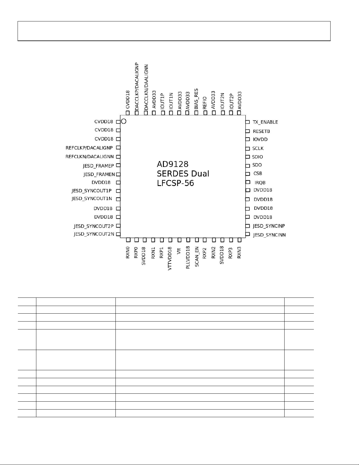
PIN CONFIGURATION AND FUNCTION DESCRIPTIONS
Figure 2.
Table 7. Pin List and Description
Pin Name Description I/O Pin
1 CVDD18 1.8V Clock Supply – Analog Clock Supply I
2 CVDD18 1.8V Clock Supply – Analog Clock Supply I
3 CVDD18 1.8V Clock Supply – PLL Supply (DAC clock generator) I
4 REFCLKP/DACALIGNP If PLL enabled, Reference Clock positive, else DAC align positive1. REFCLKP
can be AC coupled. DACALIGNP cannot be AC coupled and needs 100
ohm (LVDS) resistor
5 REFCLKN/DACALIGNN If PLL enabled, Reference Clock negative, else DAC align negative1.
REFLCKN can be AC coupled. DACALIGNN cannot be AC coupled and
needs 100 ohm (LVDS) resistor
6 JESD_FRAMEP JESD204A Compliant frame clock, positive. Can be AC coupled. I
7 JESD_FRAMEN JESD204A Compliant frame clock, negative. Can be AC coupled. I
8 DVDD18 1.8V Digital Supply – for frame clock and timing DLL. I
9 JESD_SYNCOUT1P JESD204A SYNC Signal, Positive. LVDS compliant. O
10 JESD_SYNCOUT1N JESD204A SYNC Signal, Negative. LVDS compliant. O
11 DVDD18 1.8V Digital Supply (Core) I
1
Single Edge DAC Alignment input if PLL is disabled. LVDS resistor required between this pin and REFCLK in align mode.
Rev. PrI | Page 8 of 67
I
I
Page 9

Preliminary Technical Data AD9128
12 DVDD18 1.8V Digital Supply (Core) I
13 JESD_SYNCOUT2P JESD204A SYNC Signal Auxiliary, Positive. LVDS compliant. O
14
15 RXN0 Serial Channel input 0, Negative. CML compliant. 50 ohm-terminated to
16 RXP0 Serial channel input 0, Positive. CML compliant. 50 ohm-terminated to Vtt
17 SVDD18 1.8V Deserializer Supply for RX0 and RX1 I
18 RXN1 Serial channel input 1, Negative. CML compliant. 50 ohm-terminated to
19 RXP1 Serial channel input 1, Positive. CML compliant. 50 ohm-terminated to Vtt
20 VTTVDD18 (SVDD18) 1.8V Deserializer supply (Vtt and bias generation supply) I
21 VTT SERDES Lane Input Termination Voltage. Used for supplying external
22 PLLVDD18 1.8V PLL Supply I
23 DVSS (GND) Tied to ground I
24 RXP2 Serial channel input 2, Positive . CML compliant. 50 ohm-terminated to Vtt
25 RXN2 Serial channel input 2, Negative. CML compliant. 50 ohm-terminated to
26 SVDD18 1.8V Deserializer Supply for Rx2 and RX3 I
27 RXP3 Serial channel input 3, Positive. CML compliant. 50 ohm-terminated to Vtt
28 RXN3 Serial channel input 3, Negative . CML compliant. 50 ohm-terminated to
29 JESD_SYNCINN JESD204A SYNC signal input, Negative. LVDS compliant SYNC input with
30 JESD_SYNCINP JESD204A SYNC signal input, Positive. LVDS compliant SYNC input with
31 DVDD18 1.8V Digital Supply (Core) I
32 DVDD18 1.8V Digital Supply (Core) I
33 DVDD18 1.8V Digital Supply I
34 DVDD18 1.8V Digital Supply I
35 IRQB Interrupt Request. Open Drain, Active Low Output O
36 CSB Serial Port Chip Select. Active Low (CMOS levels w.r.t. IOVDD) I
37 SDO Serial Port Data Output (CMOS levels w.r.t. IOVDD) O
38 SDIO Serial Port Data Input/Output (CMOS levels w.r.t. IOVDD) I/O
39 SCLK Serial Port Clock Input (CMOS levels w.r.t. IOVDD) I
40 IOVDD 1.8V – 3.3V Serial Port Supply I
41 RESETB Reset. Active Low. (CMOS levels w.r.t. IOVDD) I
42 TXENABLE Transmit Enable Function pin, programmable parameters through SPI. I
43 AVDD33 3.3V Analog Supply – DAC supply I
44 IOUT2P Q DAC Positive Current Output O
45 IOUT2N Q DAC Negative Current Output O
46 AVDD33 3.3V Analog Supply O
47 REFIO Voltage Reference. Nominally 1.2V output. Should be decoupled to
48 BIAS_RES External reference resistance. Used to set LVDS swing, DAC full-scale
JESD_SYNCOUT2N JESD204A SYNC Signal Auxiliary, Negative. LVDS compliant. O
I
Vtt pin voltage. Can be AC coupled. Resistance calibrated.
I
pin voltage. Can be AC coupled. Resistance calibrated.
I
Vtt pin voltage. Can be AC coupled. Resistance calibrated.
I
pin voltage. Can be AC coupled. Resistance calibrated.
I
termination voltage. Load should be < 100pF if internal voltage is used.
I
pin voltage. Can be AC coupled. Resistance calibrated.
I
Vtt pin voltage. Can be AC coupled. Resistance calibrated.
I
pin voltage. Can be AC coupled. Resistance calibrated.
I
Vtt pin voltage. Can be AC coupled. Resistance calibrated.
I
internal differential termination only. Resistance calibrated.
I
internal differential termination only. Resistance calibrated.
I
Analog Ground.
I
current, and deserializer input termination. Place 10K ohm resistor to
analog ground.
Rev. PrI | Page 9 of 67
Page 10

AD9128 Preliminary Technical Data
49 AVDD33 3.3V Analog Supply I
50 AVDD33 3.3V Analog Supply I
51 IOUT1N I DAC Negative Current Output O
52 IOUT1P I DAC Positive Current Output O
53 AVDD33 3.3V Analog Supply I
54 DACCLKN/DACALIGNN DAC Clock Negative input if PLL disabled. DAC Alignment Negative input
if PLL is enabled. DACCLKN can be AC coupled. DACALIGNN cannot be AC
coupled and needs 100 ohm (LVDS) resistor
55 DACCLKP/DACALIGNP DAC Clock Positive input if PLL disabled. DAC Alignment Positive input if
PLL is enabled. DACCLKP can be AC coupled. DACALIGNP cannot be AC
coupled and needs 100 ohm (LVDS) resistor
56 CVDD18 1.8V Supply – Clock Supply Voltage I
I
I
Rev. PrI | Page 10 of 67
Page 11

Preliminary Technical Data AD9128
TYPICAL PERFORMANCE CHARACTERISTICS
Figure 3
Figure 4
Figure 6
Figure 7
Figure 5
Rev. PrI | Page 11 of 67
Page 12

AD9128 Preliminary Technical Data
TERMINOLOGY
Integral Nonlinearity (INL)
INL is the maximum deviation of the actual analog output from
the ideal output, determined by a straight line drawn from zero
scale to full scale.
Differential Nonlinearity (DNL)
DNL is the measure of the variation in analog value, normalized
to full scale, associated with a 1 LSB change in digital input code.
Offset Error
Offset error is the deviation of the output current from the ideal
of 0 mA. For IOUT1P, 0 mA output is expected when all inputs
are set to 0. For IOUT1N, 0 mA output is expected when all
inputs are set to 1.
Gain Error
Gain error is the difference between the actual and ideal output
span. The actual span is determined by the difference between
the output when all inputs are set to 1 and the output when all
inputs are set to 0.
Output Compliance Range
The output compliance range is the range of allowable voltage
at the output of a current output DAC. Operation beyond the
maximum compliance limits can cause either output stage
saturation or breakdown, resulting in nonlinear performance.
Temperature Drift
Temperature drift is specified as the maximum change from
the ambient (25°C) value to the value at either T
MIN
or T
MAX
.
For offset and gain drift, the drift is reported in ppm of fullscale range (FSR) per degree Celsius. For reference drift, the
drift is reported in ppm per degree Celsius.
Signal-to-Noise Ratio (SNR)
SNR is the ratio of the rms value of the measured output signal
to the rms sum of all other spectral components below the Nyquist
frequency, excluding the first six harmonics and dc. The value
for SNR is expressed in decibels.
Interpolation Filter
If the digital inputs to the DAC are sampled at a multiple rate of
f
(interpolation rate), a digital filter can be constructed that
DATA
has a sharp transition band near f
appear around f
(output data rate) can be greatly suppressed.
DAC
/2. Images that typically
DATA
Adjacent Channel Leakage Ratio (ACLR)
ACLR is the ratio in decibels relative to the carrier (dBc) between
the measured power within a channel relative to its adjacent
channel.
Complex Image Rejection
In a traditional two-part upconversion, two images are created
around the second IF frequency. These images have the effect
of wasting transmitter power and system bandwidth. By placing
the real part of a second complex modulator in series with the
first complex modulator, either the upper or lower frequency
image near the second IF can be rejected.
Current Mode Logic (CML)
CML is a differential digital logic family. Signal transmission is
point-to-point, unidirectional and terminated at the destination
with 50 resistors to a voltage, VTT, on both differential lines.
CML is the physical layer for JESD204.
Power Supply Rejection (PSR)
PSR is the maximum change in the full-scale output as the
supplies are varied from minimum to maximum specified
voltages.
Settling Time
Settling time is the time required for the output to reach and
remain within a specified error band around its final value,
measured from the start of the output transition.
Spurious Free Dynamic Range (SFDR)
SFDR is the difference, in decibels, between the peak amplitude
of the output signal and the peak spurious signal within the dc
to Nyquist frequency of the DAC. Typically, energy in this band
is rejected by the interpolation filters. This specification, therefore, defines how well the interpolation filters work and the
effect of other parasitic coupling paths on the DAC output.
Rev. PrI | Page 12 of 67
Page 13

Preliminary Technical Data AD9128
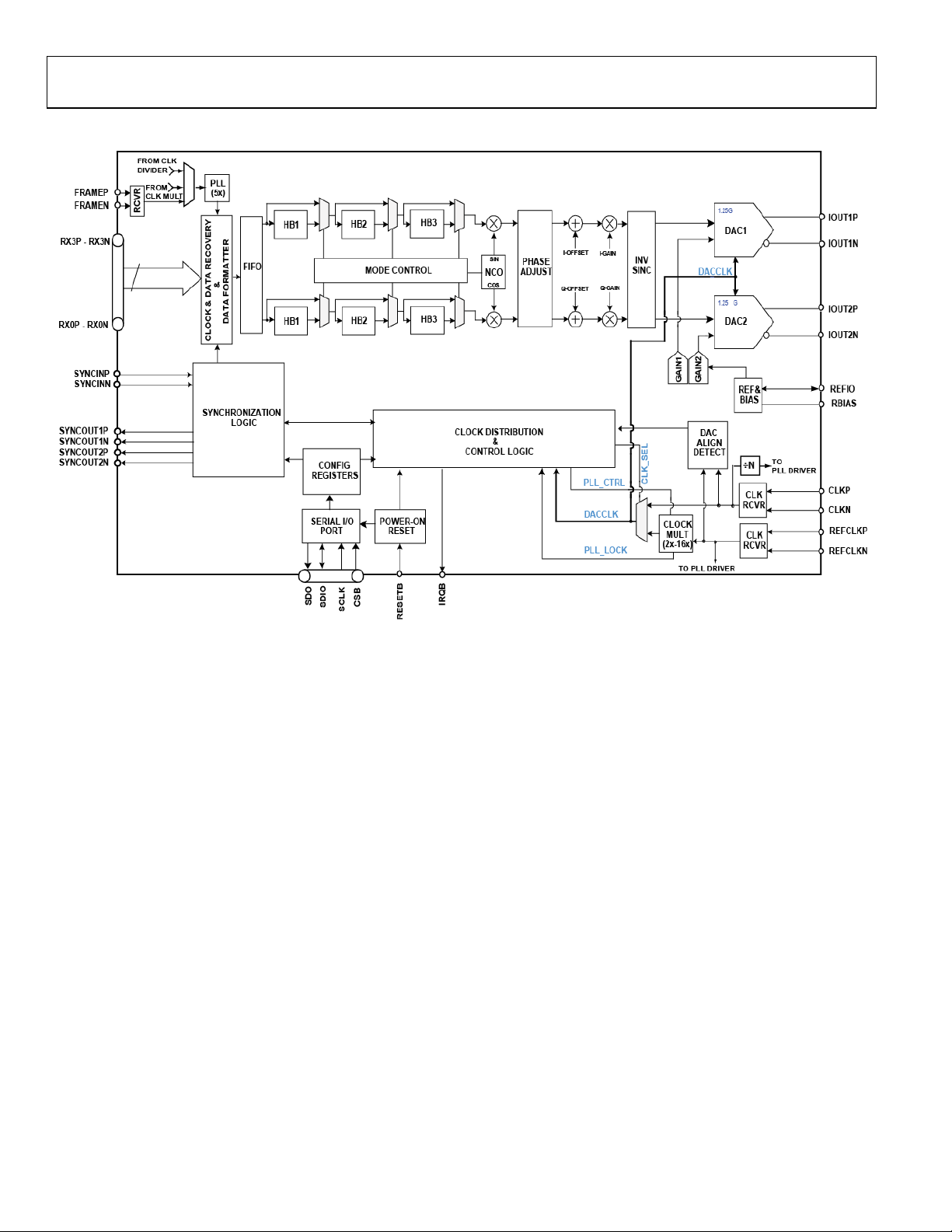
THEORY OF OPERATION
The AD9128 is a 16-bit Dual DAC with a SERDES interface that
is fully compliant with the JESD204A specifications. Figure 8
shows a top-level diagram of the AD9128. Four high-speed
serial lanes carry data with a maximum speed of 3.125Gbps,
resulting in a 312.5 MSPS (maximum) input data rate for each
of the two DACs. The AD9128 can be configured to operate in
1, 2 or 4 JESD204A lane modes, depending on the required
DAC input data rate. It can also operate in single DAC mode,
with either 1-lane or 2-lane mode.
The two DACs can operate as I and Q channels in a direct
conversion transmitter. Or as two independent DACs running
at the same DAC sampling rate. The digital data-path of the
AD9128 offers four interpolation modes (1X, 2X, 4X or 8X)
through three half-band filters with a maximum DAC sampling
rate of 1.25 GSPS.
F
is the DAC sampling frequency. The input signal data-rate for
DAC
both DACs is
For I/Q applications a Numerically Controlled Oscillator
(NCO) provides a means for modulating the signal with a
programmable carrier signal. The NCO generates the carrier
signal for a complex modulator in the digital data path. The
resolution of the NCO is 32 bits, allowing the signal to be
placed in the output spectrum with very fine resolution. The
AD9128 Startup Sequence). The following sections describe
elements of the AD9128 in detail.
F
÷
the interpolation factor.
DAC
AD9128 also features coarse modulation. Coarse modulation
up converts a digital signal centered at DC center frequency of
F
/4. This option consumes significantly less power compared
DAC
with the NCO modulation approach. Digital gain, offset and
phase compensation are included in the AD9128 to help with
unwanted sideband suppression in direct conversion
transmitters. An inverse Sinc filter is provided to compensate
for DAC output sinc-related roll-off.
The DAC Clock (DACCLK) can be sourced externally. Or
generated on chip using a PLL synthesizer with externally
supplied reference signal.
The AD9128 DAC core provides a fully differential current
output with a nominal full-scale current of 20mA. The full-scale
current is user adjustable between 8.7mA and 31.7mA. The
differential current outputs are complementary.
The AD9128 is capable of multi-chip synchronization and can
both synchronize devices and establish deterministic latency
(latency locking) among multiple AD9128 devices. The latency
for each of the DACs remains constant from link establishment
to link establishment.
A SPI interface provides read and write access to registers. The
various functional blocks and the data interface need to be
setup in a specific sequence for proper operation (See section
Rev. PrI | Page 13 of 67
Page 14
AD9128 Preliminary Technical Data
Figure 8. AD9128 Functional Block Diagram
Rev. PrI | Page 14 of 67
Page 15

Preliminary Technical Data AD9128
T
A
HIGH SPEED SERIAL DATA INTERFACE
The AD9128 has four JESD204A data ports that receive data for
both I and Q transmit paths. Figure 9 describes the
communication layers implemented in the AD9128 for each
high speed serial data interface to recover the clock, descramble
and deserialize the data before it is sent to the Digital Signal
Processing section of the AD9128. If a lower data speed is
SYNC
RX P/N
FRAME
RECEIVER LINK LAYER DESCRAMBLER
Figure 9. Functional block diagram of Serial receiver
As the AD9128 can operate with more than one active high
speed serial data lane, both achieving synchronization and
handling loss of synchronization of the lanes are very
important. To simplify the interface to the companion digital
chip, theAD9128 designates one master signal (SYNCb) as far
as multiple lane synchronization is concerned. If one lane loses
synchronization, a resynchronization request is sent to the
transmitter and the transmitter stops sending data to all lanes
until resynchronization has been achieved.
RECEIVER CIRCUIT
The AD9128 provides four 1.8V differential serial input
interfaces compliant with the JESD204A specifications. These
interfaces can accept signals at frequencies up to 3.125Gbps
using the input topology in Figure 10.
RXP
Z
2
RDIFF
Z
RDIFF
RXN
Figure 10. Receiver line termination
The receiver eye mask in Figure 11 specifies the signal
amplitude and jitter tolerance for the AD9128 High Speed Serial
Data Interface receiver.
Z
TT
2
V
T
acceptable the part can be configured to operate with either two
or one JESD204A lanes. The maximum data speed is directly
linked to the number of lanes used. In the 4 lane, 2 lane and 1
lane configurations, the maximum supported data speeds are
312.5 MSPS, 156.25 MSPS and 78.125 MSPS respectively.
I DSP + DAC
TRANSPORT
LAYER
Q DSP + DAC
500mV
87.5mV
DIFFERENTI
VOLTAG E
L
0
- 87.5mV
-500mV
0.22 / DATA RATE
0.44 / DATA RATE
Figure 11. Receiver Eye Mask
The receiver is equipped with a Clock/Data Recovery circuit
(CDR) based on a PLL. The PLL effectively multiplies the Frame
clock input by 5 X F (F=Number of bytes per frame) and the
CDR synchronizes the phase used to sample the data on each
serial lane independently. This independent phase adjustment
per serial interface ensures accurate data sampling and eases the
implementation of multiple serial interfaces on a PCB. A byte
rate PLL clock is then used in the link layer, descrambler and
transport layers to deserialize the serial input and provide data
to the DAC inputs.
LINK LAYER
The AD9128 can operate with more than one active high speed
serial data interface. Link layer communications such as code
group synchronization, frame alignment and frame
synchronization are handled by all four lanes. However, the
configuration data is always checked only on a single logical
high speed serial data interface: LN0. This logical serial
interface can be connected to any of the four JESD204A
physical receivers RXn. It is important to note that logical LN0
must be active in all modes of operation.
The AD9128 decodes 8B/10B control characters allowing
marking of start and end of frame and alignment between serial
lanes. The AD9128 serial interface can issue a synchronization
Rev. PrI | Page 15 of 67
Page 16

AD9128 Preliminary Technical Data
request by setting the SYNCb pin low. The synchronization
protocol follows the JESD204A standard. When a stream of 8
consecutive /K/ symbols is received, the AD9128 deactivates the
synchronization request by setting SYNCb pin high and waits
for the transmitter to issue an Initial Lane Alignment Sequence
(ILAS).
DESCRAMBLER
The AD9128 provides an optional descrambler block using a
self-synchronous descrambler with polynomial: 1 + x
Data scrambling can be selected at the transmitter to reduce
spectral peaks that would be produced when the same data
octets repeat from frame to frame. Another advantage of
scrambling is that it makes the spectrum data independent so
that possible frequency-selective effects on the electrical
interface will not cause data-dependent errors.
14
+ x15.
TRANSPORT LAYER
The transport layer maps the incoming descrambled data to
DAC samples. It provides control of the JESD204A parameters
shown in Table 8.
all 4 lanes cannot be used in single-DAC mode). The maximum
input data rate in single-DAC mode is the same as the dual
DAC mode (312.5MHz).
Table 10. AD9128 interface speeds
Parameter Value
Serial interface
speed
Effective serial
interface speed
3.125Gbps
2.5Gbps
# of lanes used 4 2 1
DAC Data update
rate (MHz)
312.5 156.25 78.125
Table 8. JESD204A Transport Layer Parameters
Parameter Description
F Number of bytes per frame: 1, 2 or 4 depending on
L
K Number of frame per multi-frame: K = 32 if F=1,
K=16 otherwise.
L Number of lanes per converter device: 1, 2 or 4
M Number of converter per device = 1, 2
Since the AD9128 uses the Frame input as the reference clock
for the deserializer PLL, the Frame input needs to be greater
than 50 MHz. A number of transport layer configurations are
defined to fit the AD9128 definition, as shown in
Ta bl e 9.
Table 9. JESD204A Configuration Parameters
Parameter Description
CF
Number of control words per frame clock per link
= 0. No control word is embedded with samples
CS Number of control bits per conversion sample = 0
High density user data format. Used when samples
HD
need to be split across lanes.
Set to 1 when F=1, 0 otherwise.
N Converter resolution = 16
N’ Total number of bits per sample = 16
Since the AD9128 has four high speed serial data interfaces,
several combinations of lanes per converter can be used
depending on the data rate desired.
The AD9128 can also operate in real single-DAC mode. In this
case, it can be configured in either 2-lane or 1-lane mode (Note:
Figure 12. Serial data interface with 4 lanes active
Configuration
CF=0
CS=0
F=2
HD=0
L=2
M=2
N=16
N’=16
FRAME INPUT
Configuration
CF=0
CS=0
F=4
HD=0
L=1
M=2
N=16
N’=16
IDACn[15:8]
QDACn[15:8] QDACn[7:0]QDAC
Figure 13. Serial data interface with 2 lanes active
FRAME INPUT
Figure 14. Serial data interface with 1 lane active
IDACn[7:0] IDAC
IDACn[15:8]
[15:8] IDAC
n+1
[15:8]QDAC
n+1
IDACn[7:0] QDACn[15:8] QDACn[7:0]
n+1
n+1
[7:0]
[7:0]
JESD204A SERIAL LINK ESTABLISHMENT
A brief summary of the high speed serial link establishment
process is given below. Please see the JESD204A Specifications
document (reference) for complete details.
1. Code group synchronization
a. Each receiver must locate K (K28.5) characters in its
input data stream
Rev. PrI | Page 16 of 67
Page 17

Preliminary Technical Data AD9128
b. Once 8 consecutive K characters have been detected
on all link lanes, the receiver block de-asserts the
SYNCb signal to the transmitter block.
c. The transmitter captures the change in SYNCb and
after a fixed number of frame clocks, starts the Initial
Lane Alignment Sequence (ILAS).
2. Initial Lane Alignment Sequence
a. The main purposes of this phase are to align all the
lanes of the link and verify the parameters of the link.
b. Before the link is established, each of the link
parameters is written to the receiver device to
designate how data will be sent to the receiver block.
c. ILAS consists of 4 or more multi-frames. The last
character or each multi-frame is a multi-frame
alignment character /A/
d. The first, third, and fourth multi-frames are populated
with pre-determined data values. The de-framer uses
the final /A/ of each lane to align the ends of the
multi-frames within the receiver.
e. The second multi-frame contains an R (K.28.0),
Q(K.28.4), and then data corresponding to the link
parameters.
f. Additional multi-frames can be added to ILAS if
needed by the receiver. The AD9128 uses 8 multiframes in its ILAS. (When alignment scheme or
deterministic latency are used.)
g. After the last /A/ character of the last ILAS multi-
frame data begins to be streamed.
3. Data Streaming
a. In this phase data is streamed from the transmitter
block to the receiver block.
b. Data can be optionally scrambled. Scrambling does
not start until the very first octet following the ILAS.
c. The receiver block processes and monitors the data it
receives for errors including:
i. Bad running disparity (8b/10b error)
ii. Not in Table (8b/10b error)
iii. Unexpected control-character
iv. Bad ILAS
v. Inter-lane skew error (through character
replacement)
d. If any of these errors exists, it is reported back to the
transmitter in one of a few ways
i. SYNCb assertion: Resynchronization (SYNCb
pulled low) is called for at each error. For the first
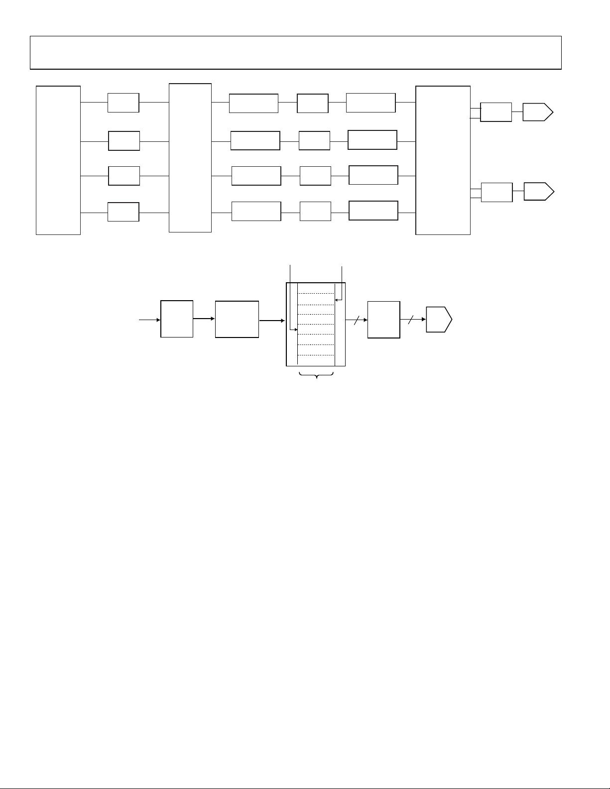
FIFO OPERATION
The AD9128 contains several stages of FIFO to deal with the
high speed serial data interface protocol and to synchronize the
data input with the DAC clock input (See Figure 15).
The FIFO in the SERDES deframer interface is used to
synchronize the samples sent on the high speed serial data
interface with the deframer clock. This FIFO absorbs timing
variations between the data source and the deframer. When the
FIFO reaches either full or empty state, it is recommended that
the user reset it through Register 35 bit 0 and, if necessary, reestablish the SERDES data link. Note that resetting the SERDES
link does not reset the FIFO to half-full automatically.
A second 2 channel x 16-bit wide, 8- word deep FIFO exists in
the DAC (datapath FIFO) to absorb timing variations between
the DAC clock and the Deframer clock. Figure 16 shows the
block diagram of the data path through the FIFO. The data is
latched into the device, formatted and then written into the
FIFO register determined by the FIFO write-pointer. The value
of the write-pointer is incremented every time a new word is
loaded into the FIFO. Meanwhile, data is read from the FIFO
register determined by the read-pointer and fed into the digital
datapath. The value of the read-pointer is updated every rising
edge of the internal DAC based data clock. The one exception
to this occurs when a resynchronization request is in progress:
the write side of the FIFO does not increment and the read side
is held in reset at a fixed value. Once the ILAS is completed in
the AD9128, then the Datapath FIFO is automatically reset to
“half full”. During a synchronization request, the DAC outputs
are forced to mid-scale and the datapath is flushed. This is done
to prevent corrupted data from passing from the DAC.
Valid data will be transmitted through the FIFOs as long as the
FIFOs do not overflow or become empty. Nominally, data will
be written to the FIFO at the same rate as data is read from the
FIFO. This keeps the data level in the FIFO constant. If data is
written to the FIFO faster than data is read, the data level in the
FIFO increases. If the data is written to the device slower than
data is read, the data level in the FIFO decreases.
three errors, SYNCb is asserted after an error
counter reaches a given error threshold.
ii. SYNCb reporting: SYNCb is pulsed low for a frame
clock period if an error occurs
iii. Reporting may also be done via interrupt (not
covered by the JESD204A specification). See (i) for
error thresholds.
Rev. PrI | Page 17 of 67
Page 18
AD9128 Preliminary Technical Data
R
CHARACTER
ALIGNMENT
CHARACTER
ALIGNMENT
CHARACTER
ALIGNMENT
CHARACTER
ALIGNMENT
RECEIVER
FIFO
FIFO
XBAR
FIFO
FIFO
Figure 15. Block Diagram of AD9128 FIFOs
INPUT
LATCH
DATA
ASSEMBLER
Figure 16 – Block Diagram of Datapath FIFO
FRAME CLOCKING
The frame clock is the master reference for the high speed serial
interface of the AD9128. It drives a PLL in the JESD204A part of
the system and needs to be set to the input data rate of the
system. The user has three options for the frame clock in
AD9128:
Externally sourced through pins JESD_FRAMEP/N: the
input should be AC coupled and will be self-biased
internally.
Externally sourced through REFCLKP/N: this is possible
only if the internal DAC PLL is used and the supplied
reference clock supplied to the PLL (via REFCLKP/N) is at
the data rate of the system. (abd equal to the FRAME rate)
The input should be AC coupled and will be self-biased
internally.
Internally sourced by using a divided down version of the
DAC clock: this helps minimize the number of low
frequency clocks in the user system.
The frame clock source is controlled and monitored through
register 0x001D.
SERDES PLL
The SERDES PLL generates clocks at half the rate of the serial
data rate and supplies them to the Clock and Data Recovery
Rev. PrI | Page 18 of 67
10-BIT/
8-BIT
10-BIT/
8-BIT
10-BIT/
8-BIT
10-BIT/
8-BIT
WRITE POINTER
READ POINTE
REG 0
REG 1
REG 2
REG 3
REG 4
REG 5
REG 6
REG 7
64-BITS
FIFO
DESCRAMBLE
DESCRAMBLE
DESCRAMBLE
DESCRAMBLE
16
DATA
PAT HS
SAMPLE RECONSTRUCTION
16
DACS
FIFO
FIFO
DAC
DAC
(CDR) block. The SERDES PLL settings are controlled and
monitored in the register 0x01E. The PLL divide ratio (register
0x01E, bits [3:0]) is dependent on the F value (number of bytes
per frame) of the JESD204A link. The F value of the link (1,2 or
4) should be written to this register. The SERDES PLL can be
monitored for lock by reading register 0x01E, bit 6.
The SERDES PLL lock can also be accessed through the
interrupt controller by writing Register 0x006, bits 7 and/or 6
high. Bit7 enables the interrupt if the SERDES PLL has lost lock,
and Bit6 enables the interrupt if the SERDES PLL is locked.
These interrupts can be found by reading register 0x009 bits 7
and 6 (when the interrupt output of the AD9128 falls,).
Note that the SERDES PLL must lock before parameters can be
written to the deframer.
CONFIGURING THE JESD204A SERIAL INTERFACE
After the SERDES PLL has been successfully locked, the
Deserializer SPI is available and can be verified by reading
register 0x02 bit 0. The Deserializer SPI is a synchronous
read/write SPI (See section Serial Peripheral Interface for SPI
interface details). It is addressed through the long addressing
mode (default for the AD9128). The addresses for this part of
the circuit range from 0x100-0x17F.
Page 19

Preliminary Technical Data AD9128
Input termination
The AD9128 will auto-calibrate to 50 ohms termination on
power-up as register 0x010 bit 5 has a default setting of high.
The auto-calibrated value found will be held constant until bit 5
is disabled. Alternatively, a manual calibration value can be
entered through register 0x011 bit 3:0 (highest resistor value is
0000 and lowest value is 1111). Manual calibration requires
register 0x10 bit5 to be low and 0x11 bit4 to be high. All settings
for input termination can be setup and controlled through
registers 0x010 and 0x011.
The input termination voltage of the DAC can be sourced either
externally or internally:
External: An external voltage can be driven through the
VTT pin. In order to support DC compliance, its value
should match the common mode voltage of the CML
driver at the transmitter. It may be bypassed at the pin
to local ground.
Internal: The termination voltage can be supplied
internally by enabling register 0x010 bit 4. The VTT
buffer drives both the internal VTT termination and
the VTT pin. The termination voltage value can be set
through register 0x010 its 3:0. In this case, the VTT pin
should not be bypassed to ground. As in option 1, to
meet DC compliance, the value of the voltage should be
chosen to be close to the value of the CML driver
output common-mode. This will ensure minimum
power consumption.
For AC coupled systems, in order to minimize power
consumption, VTT should be set close to 600mV.
Clock Data Recovery (CDR)
The CDR circuits for the four lanes of the high speed serial
interface can be enabled through register 0x012 bits 3:0. For
two-lane or one-lane operation, any of the two or any one lane
can be chosen. Unused lanes, if enabled, will consume
unnecessary power.
Logical Lane Mapping/Enabling
Each of the four physical high speed serial interface lanes, if
used, must be mapped to an appropriate logical lane. For
example, if four physical lanes are enabled for use with two
converters then each of the four logical lanes are mapped to a
distinct physical lane. Logical lanes 0, 1, 2 and 3 will contain
IMSB, ILSB, QMSB, QLSB respectively. The logical lanes are
enabled through register 0x17D and their mapping is controlled
through register 0x016, as shown in Tab l e 11.
Table 11. Logical lane mapping for JESD204A link
Rev. PrI | Page 19 of 67
AD9128
configuration
# of
Lanes
# of
DAC
4 2 Each physical lane is mapped to a
2 2 Logical 0 should be mapped to the
data I serial input and logical 2 to
the data Q serial input. Logical
lanes 3 and 4 are unused in this
2 1 Logical 0 should be mapped to
data MSBs and logical 2 to the data
1 2 Logical 0 should to be mapped to
the one serial link and others are
1 1 Logical 0 should both be mapped
to the input lane carrying data
Description Reg.
0x017
D value
0x0F
distinct logical lane
0x05
case
0x05
LSBs
0x01
ignored
0x01
Each of the input lanes can be individually controlled as far as
serial symbol mapping is concerned. Both the ordering of the
bits (MSB to LSB or LSB to MSB) on bits 7:4, and the individual
polarities on bits 3:0 are controlled through register 0x017.
A few mode bits are required in order to operate the non default
mode of 4 Lanes or 2 Lanes and F = 1. These are contained in
the Register 0x177. They enable sub-modes of the base
configuration of the deframer:
If F=2, Register 0x177 bits 5:2 must be set to 0111 (1 lane
per DAC) and 0x176 must be set to 2.
If F=4, Register 0x177 bits 5:2 must be set to 1011 (2 DACs
1 line) and 0x176 must be set to 4.
If F=1, Register 0x177 bits 5:2 must be set to 0000
Programming the JESD204A link parameters
This section provides details of the link parameters with respect
to the modes of operations supported by the AD9128. The link
parameters are programmed through registers 0x150 to 0x15D.
In order to achieve an accurate comparison, all the register
values must be programmed the same at the transmitter and
receiver end of the link.
1. 0x150: Provides the DID (Device ID or link ID). This is a
comparison only value to identify the link name.
2. 0x151 bits 3:0: Provides the BID (Bank ID). It is an
extension of the DID and meets the same requirements as
the DID.
3. 0x152 bits 3:0: Provides the LID0 (lane ID for lane 0 within
a link). The AD9128 will check the lane identification
values on lane 0 only.
4. 0x153 bit7: Enables the scrambling function on the link.
5. 0x153 Bits4:0: Provides the number of lanes of the link
associated with DID. This value L will be set based on the
number of lanes used and is programmed as one less than
Page 20
AD9128 Preliminary Technical Data
the number of lanes. The possible values for different DAC
modes are:
4 Lanes, 2 DACs L=3
2 Lanes, 2 DACs L=1
1 Lane, 2 DACs L=0
2 Lanes, 1 DAC L=1
1 Lane, 1 DAC L=0
6. 0x154: Provides the F value or number of octets per frame
per lane. Possible values for different modes are shown in
Table 12.
Table 12. JESD204A link “F” value
AD9128 configuration JESD204A
F parameter
# of Lanes # of DAC
Register
0x0154
value
4 2 0 1
2 2 1 2
1 2 3 4
2 1 0 1
1 1 1 2
7. 0x155 bits4:0: Provide the K value (number of frames in a
multiframe). This value is programmed at one less than the
actual number. For the AD9128, the value can be:
K = 31 when F = 0 - 0x1F
K = 31 or 15 when F = 1 or 3- 0x1F or 0x0
8. 0x156: Provides the value of M (number of converters on
the DAC used by the link). This value is programmed as
one less than the actual number of converters.
2 Converters – 0x01
1 Converter – 0x00
2 Lanes, 1 DAC HD = 1 (0x15A = 0x80
1 Lane, 1 DAC HD = 0 (0x15A = 0x00)
9. 0x157 bits 7:6: Provide number of control words per frame.
For the AD9128, this value is always 0 since it does not
support control bits.
10. 0x157 bits 5:0: Represents the number of bits of resolution
of the converter. It is programmed at one less than the
actual value. The value is 0x0F for the AD9128.
INTERRUPT
ENA REGISTER
INTERRUPT
EDGE
DETECTOR
INTERRUPT
SOURCE
Figure 21. Interrupt control on the AD9128
11. 0x158 bits 5:0: Represents the number of bits in each
sample being sent to the deframer. It is programmed at one
less than the actual value. The value is 0x0F for the
AD9128.
12. 0x159: Represents the number of samples per frame per
converter and is programmed as one less than actual. The
AD9128 supports only S = 1 (Reg. 0x159 set to 0).
13. 0x15A bit 7: Represents the high density HD parameter.
ENA = 0
ENA = 1
ISR
READ BACK
INTERRUPT
OTHER
INTERRUPTS
IRQ
14. 0x15A bits 4:0: Represents CF (the number of control
words per frame clock per lane). Possible values for register
0x15A are shown in Table 13.
Table 13. JESD204A link “HD” value
Rev. PrI | Page 20 of 67
Page 21

Preliminary Technical Data AD9128
AD9128 configuration JESD204A
HD parameter
# of Lanes # of DAC
4 2 1 0x80
2 2 0 0x00
1 2 0 0x00
2 1 1 0x80
1 1 0 0x00
15. 0x15B, 0x15C: Reserved fields. Should be set to 0 on both
receiver and transmitter ends.
16. 0x15D: Checksum value equal to the sum of all the
registers from 0x150 to 0x15C modulo 256.
Programming ILAS (Initial Lane Alignment Sequence)
length:
In the AD9128 the length of the ILAS is programmed in register
0x178. It is programmed as the actual number of multi-frames
times four (for a value of 1, the ILAS will be 4 multi-frames
long). The AD9128 uses 8 multi-frames during the ILAS to
accomplish multichip alignment (or 4 if multi-chip alignment is
not needed).
In order to enable multichip alignment or latency locking,
register 0x178 should be set to 0x02 and register 0x17B bit 0
should be set to 1. When latency locking/alignment is not
needed in the system, register 0x178 should be set to 1 and
0x17B bit 0 to 0.
Register
0x015A
value
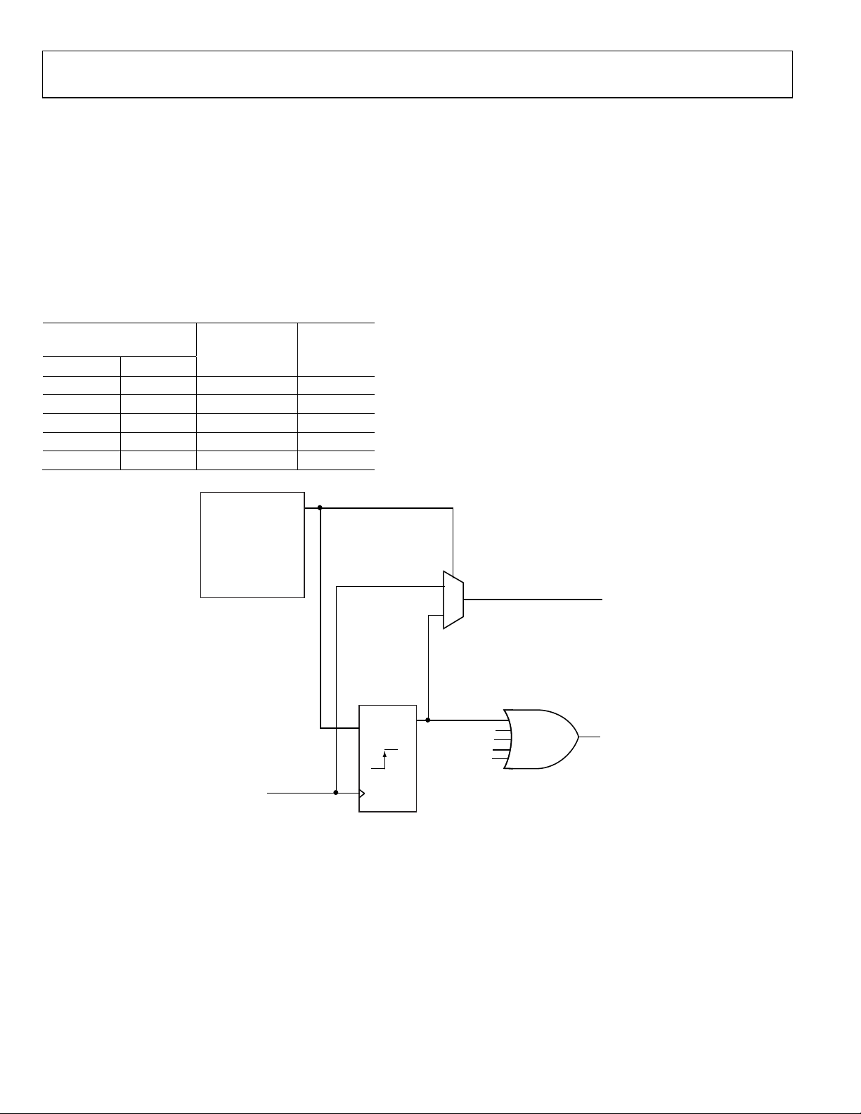
INTERRUPTS AND SYNCB CONTROL
The deframer monitors the link for errors, and in the AD9128
these errors can be reported back to the transmitter through
different methods:
Through interrupts
Through the SYNCb signal as frame width assertion
pulses on the line
Through the SYNCb interface as forced SYNC requests.
Figure 27 shows a block diagram of the AD9128 interrupt
control. Errors are counted on a lane by lane basis and either an
error interrupt or a SYNCb event is triggered as the count
reaches an Error Threshold. This threshold is programmed in
Register 0x17C. Error counts for each lane can be monitored
through the use of Registers 0x16D – 0x16F. The errors that the
deframer will detect are: Bad Disparity Error, Not in Table
Error, Unexpected control character, Alignment issue, Bad ILS
Sequence, Configuration mismatch
The Interrupt request is masked by bits in registers 0x17A and
0x17B as follows:
0x17A, Bit7 – Bad Disparity (set high to trigger Interrupt
request)
0x17A, Bit 6 – Not in Table
0x017A, Bit 5 – Unexpected control character
0x017A, Bit 4 – Interlane Alignment good
Rev. PrI | Page 21 of 67
0x017A, Bit 3 – Good ILAS sequence
0x017A, Bit2 – Good Checksum
0x017A, Bit1 – Good Frame Sync
0x017A, Bit0 – Good Code Group Sync
The SYNCb frame width error reporting can be enabled by
setting bit 1 of Register 0x175 high (Bad disparity, not in Table,
and Unexpected control character will actuate this error
reporting mode).
The SYNC force is masked by bits in 0x17B as follows:
0x17B, Bit7 – Bad disparity error (set high for error to force
SYNCb high upon error threshold)
0x17B, Bit6 – Not in Table error
0x17B, Bit5 - Unexpected control character
ENABLING THE LINK
Once SYNCb setup/calibration is completed and clocks have
settled, the link is ready to be established. The link can be
established by setting bit 7 of Register 0x00A high. A startup
sequence is performed for the delay path from DAC clock to
SYNCb.
1. The SYNCb phase selector is reset to zero
2. The SYNCb FIFO is reset.
3. The previously programmed value of the SYNCb
launch phase is programmed back to the SYNCb
phase selector.
Once the startup sequence concludes inside the DAC, the
SYNCb signal is allowed to fall. Conditional upon the link
parameters being consistent at both ends and the DAC being
able to capture data, the link will be established.
Page 22

AD9128 Preliminary Technical Data
SERIAL PORT INTERFACE
Serial Port Operation
The serial port is a flexible, synchronous serial communications
port allowing easy interface to many industry-standard microcontrollers and microprocessors. The serial I/O is compatible
with most synchronous transfer formats, including both the
Motorola SPI® and Intel® SSR protocols. The interface allows
read/write access to all registers that configure the AD9128.
Single or multiple byte transfers are supported, as well as MSBfirst or LSB-first transfer formats. The serial interface ports can
be configured as a single pin I/O (SDIO) or two unidirectional
pins for input/output (SDIO/SDO).
50
SDO
51
SDIO
SCLK
Figure 17. Serial Port Interface Pins
There are two phases to a communication cycle with the
AD9128. Phase 1 is the instruction cycle (the writing of an
instruction byte into the device), coincident with the first eight
SCLK rising edges. The instruction byte provides the serial port
controller with information regarding the data transfer cycle,
Phase 2 of the communication cycle. The Phase 1 instruction
byte defines whether the upcoming data transfer is a read or
write and the starting register address for the first byte of the
data transfer. The first eight SCLK rising edges of each
communication cycle are used to write the instruction byte into
the device.
A logic high on the
CS
pin followed by a logic low resets the
serial port timing to the initial state of the instruction cycle.
From this state, the next eight rising SCLK edges represent the
instruction bits of the current I/O operation.
The remaining SCLK edges are for Phase 2 of the
communication cycle. Phase 2 is the actual data transfer
between the device and the system controller. Phase 2 of the
communication cycle is a transfer of one or more data bytes.
Registers change immediately upon writing to the last bit of
each transfer byte, except for the frequency tuning word and
NCO phase offsets that only change when the frequency update
bit (Register 0x026, Bit 0) is set.
Table 14. Serial Port Instruction Byte
I7
(MSB)
R/W A6 A5 A4 A3 A2 A1 A0
I6 I5 I4 I3 I2 I1 I0
CS
SPI
PORT
52
53
08281-010
(LSB)
Rev. PrI | Page 22 of 67
Data Format
The instruction byte contains the information shown in
14
. R/W, Bit 7 of the instruction byte determines whether a
Table
read or a write data transfer occurs after the instruction byte
write. Logic 1 indicates a read operation, and Logic 0 indicates a
write operation.
A6 to A0, Bit 6 to Bit 0 of the instruction byte, determine the
register that is accessed during the data transfer portion of the
communication cycle. For multibyte transfers, A6 is the starting
byte address. The remaining register addresses are generated by
the device based on the LSB_FIRST bit (Register 0x000, Bit 6).
SERIAL PORT PIN DESCRIPTIONS
Serial Clock (SCLK)
The serial clock pin synchronizes data to and from the device
and runs the internal state machines. The maximum frequency
of SCLK is 40 MHz. All data input is registered on the rising
edge of SCLK. All data is driven out on the falling edge of
SCLK.
Chip Select (CS)
An active low input starts and gates a communication cycle.
It allows more than one device to be used on the same serial
communications lines. The SDO and SDIO pins go to a high
impedance state when this input is high. During the
communication cycle, chip select should stay low.
Serial Data I/O (SDIO)
Data is always written into the device on this pin. However, this
pin can be used as a bidirectional data line. The configuration
of this pin is controlled by Register 0x000, Bit 7. The default is
Logic 0, configuring the SDIO pin as unidirectional.
Serial Data Out (SDO)
Data is read from this pin for protocols that use separate lines
for transmitting and receiving data. In the case where the
device operates in a single bidirectional I/O mode, this pin does
not output data and is set to a high impedance state.
Serial Port Options
The serial port can support both MSB-first and LSB-first data
formats. This functionality is controlled by LSB_FIRST
(Register 0x000, Bit 6). The default is MSB-first (LSB_FIRST =
0).
When LSB_FIRST = 0 (MSB-first), the instruction and data bit
must be written from MSB to LSB. Multibyte data transfers in
MSB-first format start with an instruction byte that includes
the register address of the most significant data byte.
Subsequent data bytes should follow from the high address to
low address. In MSB-first mode, the serial port internal byte
address generator decrements for each data byte of the
multibyte communication cycle.
Page 23

Preliminary Technical Data AD9128
K
K
When LSB_FIRST = 1 (LSB-first), the instruction and data bit
must be written from LSB to MSB. Multibyte data transfers in
LSB-first format start with an instruction byte that includes the
register address of the least significant data byte followed by
multiple data bytes. The serial port internal byte address
generator increments for each byte of the multibyte
communication cycle.
INSTRUCTIO N CYCLE DATA TRANSFER CYCLE
CS
SCLK
SDIO
SDO
R/W A6 A5 A4 A3 A2 A1 A0 D7 D6ND5
D7 D6ND5
N
N
D00D10D20D3
0
D00D10D20D3
0
Figure 18. Serial Register Interface Timing MSB-First
INSTRUCTIO N CYCLE DATA TRANSFER CYCLE
CS
SCLK
SDIO
SDO
A0 A 1 A2 A3 A4 N0 N1 R/W D00D10D2
D00D10D2
0
0
Figure 19. Serial Register Interface Timing LSB-First
D7ND6ND5ND4
N
D7ND6ND5ND4
N
08281-011
08281-012
The serial port controller data address decrements from the
data address written toward 0x00 for multibyte I/O operations
if the MSB-first mode is active. The serial port controller
address increments from the data address written toward 0x7F
for multibyte I/O operations if the LSB-first mode is active.
t
SCL
SDIO
CS
DS
t
DS
t
PWH
t
t
SCLK
t
PWL
DH
INSTRUCTION BIT 6INSTRUCTIO N BIT 7
Figure 20. Timing Diagram for Serial Port Register Write
CS
SCL
t
DV
SDIO,
SDO
Figure 21. Timing Diagram for Serial Port Register Read
DATA BIT n – 1DATA BIT n
08281-013
8281-014
Rev. PrI | Page 23 of 67
Page 24

AD9128 Preliminary Technical Data
DIGITAL DATA PATH
HB1 HB2 HB3
Figure 22 –Block Diagram of digital datapath
Figure 22 shows the functionality of the digital datapath. The
digital processing includes three half-band interpolation filters,
a quadrature modulator with a fine resolution NCO, Phase and
Offset adjustment blocks and an inverse sinc filter.
The digital datapath accepts I and Q data streams and processes
them as either two real data streams or as a quadrature data
stream. To utilize any of the modulation modes, the data must
be presented to the device in quadrature. The datapath can be
used to process two independent real data streams with any of
the interpolation modes. The coarse modulation (Fs/4) block
can be used along with any of the interpolation filter modes.
INTERPOLATION FILTERS
The transmit path contains three interpolation filters. Each of
the three interpolation filters provides a 2x increase in output
data rate. The half-band (HB) filters can be cascaded or
bypassed to provide 1x, 2x, 4x or 8x interpolation ratios. The
bandwidth of the three half-band filters with respect to the data
rate at the filter input is as follows:
Bandwidth of HB1 = 0.8xf
Bandwidth of HB2 = 0.5xf
Bandwidth of HB3 = 0.4xf
The usable bandwidth is defined as the frequency over which
the filters have a passband ripple of less than +/-0.01dB and an
image rejection of greater than 85dB.
The fine modulator performs frequency translation by
performing a digital quadrature modulation of the input signal
with a quadrature LO generated by the on-chip NCO.
1. 2x interpolation: Either the first (HB1) or second
(HB2) half-band filter can be used for 2x interpolation
(Register 0x00F). Figure 18 and Figure 19 show the
frequency response when HB1 and HB2 are used
respectively. The frequency (x-axis) is normalized to
the DAC sample rate. Hence in this case, the
bandwidth of HB1 is 0.4*Fdac or 0.8*Fdata. Similarly,
the bandwidth of HB2 is 0.25*Fdac or 0.5*Fdata
2. 4x interpolation: It is accomplished using HB1 and
HB2 (Register 0x00F). Note that it is not possible to
use HB3 when in 4x interpolation mode. Figure 20
shows the frequency response for this case. The usable
bandwidth is 0.2*Fdac or 0.8*Fdata.
IN1
IN2
IN3
PHASE
F
4
S
AND
OFFSET ADJ.
.
SINC
-1
3. 8x interpolation: In this case, all three filters are used.
Figure 21 shows the frequency response for 8x
interpolation. The usable bandwidth is 0.1*Fdac or
0.8*Fdata.
Table 15. AD9128 interpolation modes
Interpolation Mode Filters used Usable bandwidth
2x HB1 (0.8 x Fdata) or (0.4
x Fdac)
HB2 (0.5 x Fdata) or (0.25
x Fdac)
4x HB1,2 (0.8 x Fdata) or (0.2
x Fdac)
8x HB1,2,3 (0.8 x Fdata) or (0.1
x Fdac)
Figure 23. Transfer Function of HB1 in 2x interpolation mode. The
frequency axis is normalized to the DAC sample rate.
Rev. PrI | Page 24 of 67
Page 25

Preliminary Technical Data AD9128
Figure 24 Transfer Function of HB2 in 2x interpolation mode. The
frequency axis is normalized to the DAC sample rate.
Figure 25 Transfer Function of HB1 and HB2 (cascaded) in 4x
interpolation mode. The frequency axis is normalized to the DAC
sample rate.
Figure 26 Transfer function of cascaded HB1, HB2 and HB3 in 8x
interpolation mode
Figure 27 Pass band and stop-band characteristics of HB1. All
three filters have pass-band ripple <0.01dB and image rejection
> 85 dBc
Rev. PrI | Page 25 of 67
Page 26

AD9128 Preliminary Technical Data
FINE MODULATION
The fine modulation makes use of a numerically controlled
oscillator, a phase shifter and a complex modulator to provide a
means for modulating the signal by a programmable carrier
signal. A block diagram of the fine modulator is shown in
Figure 28. The fine modulator, in conjunction with the coarse
modulator allows the signal to be placed anywhere in the output
spectrum with very fine frequency resolution.
The quadrature modulator is used to mix the carrier signal
generated by the NCO with the I and Q signals. The NCO
produces a quadrature carrier signal to translate a single
sideband of the input signal to a new center frequency. A
complex carrier signal is a pair of sinusoidal waveforms of the
same frequency, offset 90° from each other. The frequency of
the complex carrier signal is set via the Frequency Tuning Word
[31:0] value in Registers 0x020 thru 0x023.
The NCO operating frequency, f
the complex carrier signal can be set up to ½ f
calculated as follows:
31
For
20 FTW
,
f
NCO
FTW
32
2
, is f
. The frequency of
DAC
f
DACCarrier
NCO
and is
For
Updating the Frequency Tuning Word
Unlike the other configuration registers, the frequency tuning
word registers do not get updated immediately upon writing.
After loading the FTW registers with the desired values, bit 0 of
register 0x026 must transition from a 0 to a 1 for the new FTW
to take effect.
Phase Offset Adjustment
A 16-bit phase offset may be added to the output of the phase
accumulator via the serial port. This static phase adjustment
results in an output signal that is offset by a constant angle
relative to the nominal signal. This allows the user to phase
align the NCO output with some external signal, if necessary.
This can be especially useful when NCOs of multiple AD9128
devices are programmed for synchronization. The phase offset
allows for the adjustment of the output timing between the
devices. The static phase adjustment is sourced from the NCO
Phase Offset Word [15:0] value located in Registers 0x024 and
0x025.
3231
,
22 FTW
f
1
FTW
32
2
f
DACCarrier
Figure 28 – Fine Modulator Block Diagram
COARSE MODULATION
The coarse modulation block at the end of the digital datapath
provides a digital up-conversion of the incoming data by ¼ of
its data rate (which is equal to Fdac, the DAC sampling rate).
When a fixed up-conversion of Fs/4 is required, the NCO can
be turned off and the coarse modulation block can be used.
Rev. PrI | Page 26 of 67
This will result in reduced power consumption. The setting for
coarse modulation can be found in Register 0x00F, bit 4.
QUADRATURE PHASE CORRECTION
The purpose of the quadrature phase correction block is to
enable compensation of the phase imbalance of the analog
quadrature modulator following the DAC. If the quadrature
Page 27

Preliminary Technical Data AD9128
A
modulator has a phase imbalance, the unwanted sideband
appears with significant energy. Tuning the Quadrature Phase
Adjust value can optimize image rejection in single sideband
radios.
Ordinarily, the I and Q channels have an angle of precisely 90°
between them. The Quadrature Phase Adjustment is used to
change the angle between the I and Q channels. When the I
Phase Adj[9:0] is set to 1000000000b, the I DAC output moves
approximately 1.75° away from the Q DAC output, creating an
angle of 91.75° between the channels. When the I Phase
Adj[9:0] is set to 0111111111b, the I DAC output moves
approximately 1.75° towards the Q DAC output, creating an
angle of 88.25° between the channels.
The Q Phase Adj[9:0] works in a similar fashion. When the Q
Phase Adj[9:0] is set to 1000000000b, the Q DAC output moves
approximately 1.75° away from the I DAC output, creating an
angle of 91.75° between the channels. When the Q Phase
Adj[9:0] is set to 0111111111b, the Q DAC output moves
approximately 1.75° towards the I DAC output, creating an
angle of 88.25° between the channels.
Based on these two endpoints, the combined resolution of the
phase compensation register is approximately 7°/2048 or
0.00342° per code. The phase adjustment bits can be found in
Registers 0x028 and 0x029.
DC OFFSET CORRECTION
The dc value of the I datapath and the Q datapath can be
independently controlled by adjusting the I DAC Offset [15:0]
and Q DAC Offset [15:0] values in Registers 0x02A thru 0x02B.
These values are added directly to the datapath values. Care
should be taken not to overrange the transmitted values.
65535. Because I
outputs, the sum of I
INVERSE SINC FILTER
The inverse sinc (sinc-1) filter is a 9-tap FIR filter. The
composite response of the sinc
DAC is shown in Figure 30. The composite response has less
than ±0.05 dB pass-band ripple up to a frequency of 0.4 ×
f
. To provide the necessary peaking at the upper end of the
DACCLK
pass band, the inverse sinc filters shown have an intrinsic
insertion loss of about 3.2 dB.
FILTERA: [17 - 53 154 -572 6596 -572 154 -53 17]
TUDE (Db)
MAGN
Figure 30. Sample composite responses of the sinc-1 filter with sin(x)/x roll-off
OUTP
and I
OUTP
are complementary current
OUTN
and I
OUTN
-1
NORMALIZ ED FREQUENCY
is always 20 mA.
and the sin(x)/x response of the
FILTERA
20
15
(mA)
10
OUTx_P
I
5
0
0x0000 0x4000 0x8000 0xC000 0xFFF F
Figure 29. DAC Output Currents vs. DAC Offset Value
DAC OFFSET VALUE
0
5
(mA)
10
OUTx_N
I
15
20
07098-108
Figure 29 shows how the DAC offset current varies as a
function of the I DAC Offset [15:0] and Q DAC Offset [15:0]
values. With the digital inputs fixed at midscale (0x0000, twos
complement data format), the figure shows the nominal I
and I
currents as the DAC offset value is swept from 0 to
OUTN
OUTP
Rev. PrI | Page 27 of 67
Page 28

AD9128 Preliminary Technical Data
DAC CLOCK CONFIGURATION
The AD9128 DAC sample clock (DACCLK) can be sourced
directly or by clock multiplying. Clock multiplying employs the
on-chip Phase Locked Loop (PLL) that accepts a reference clock
operating at a sub-multiple of the desired DACCLK rate, most
commonly the data input frequency. The PLL then multiplies
the reference clock (REFCLK, provided through REFCLKP/N
pins) up to the desired DACCLK frequency, which can then be
used to generate all the internal clocks required by the DAC.
The clock multiplier provides a high quality clock that meets
the performance requirements of most applications. Using the
on-chip clock multiplier removes the burden of generating and
distributing the high speed DACCLK.
The second mode bypasses the clock multiplier circuitry and
allows DACCLK to be sourced directly to the DAC core. This
mode enables the user to source a very high quality clock
directly to the DAC core. Sourcing the DACCLK directly
through the DACCLKP, and DACCLKN pins may be necessary
in demanding applications that require the lowest possible DAC
output noise, particularly when directly synthesizing signals
above 150 MHz.
Note that the AD9128 also requires a Frame clock
(JESD_FRAMEP/N) that is used as the master clock for the
serial interface. The REFCLK and DACCLK pins are dual-use
pins: when not in use, they can be used for DAC alignment
(DACALIGNP/N).
DRIVING THE DACCLK, REFCLK AND FRAME
INPUTS
The REFCLK and DACCLK differential inputs share similar
clock receiver input circuitry. Figure 31 shows a simplified
circuit diagram of the input. The on-chip clock receiver has a
differential input impedance of about 10 kΩ. It is self biased to a
common-mode voltage of about 1.25 V (LVDS compliant). The
inputs can be driven by direct coupling differential PECL or
LVDS drivers. The inputs can also be ac-coupled if the driving
source cannot meet the input compliance voltage of the receiver.
CLKP
5KΩ
5KΩ
CLKN
Figure 31. Clock Receiver input equivalent circuit.
1.25V
If either REFCLKP/N or DACCLKP/N is used for the
DACALIGN function, an external 100ohm resistor must be
supplied between the two pins (DACALIGNP/DACALIGNN).
The minimum input drive level to either of the clock inputs is
200 mV p-p differential. The optimal performance is achieved
when the clock input signal is between 800 mV p-p differential
and 1.6 V p-p differential. Whether using the on-chip clock
multiplier or sourcing the DACCLK, directly, it is necessary that
the input clock signal to the device has low jitter and fast edge
rates to optimize the DAC noise performance.
DIRECT CLOCKING
Direct clocking with a low noise clock produces the lowest
noise spectral density at the DAC outputs. To select the
differential CLK inputs as the source for the DAC sampling
clock, set the PLL enable bit (Register 0x018, Bit[7]) to 0. This
powers down the internal PLL clock multiplier and selects the
input from the DACCLKP and DACCLKN pins as the source
for the internal DAC sample clock.
The device also has duty-cycle correction circuitry and
differential input level correction circuitry. Enabling these
circuits can provide improved performance in some cases.
The control bits for these functions can be found in Register
0x019.
CLOCK MULTIPLICATION
The on-chip PLL clock multiplier circuit can be used to
generate the DAC sample rate clock from a lower frequency
reference clock. When the PLL enable bit (Register 0x018,
Bit[7]) is set to 1, the clock multiplication circuit generates the
DAC sample clock from the lower rate REFCLK input. The
functional diagram of the clock multiplier is shown in Figure
32. The PLL can be setup and controlled through registers
0x018, 0x01A, and 0x01B.
The clock multiplication circuit operates such that the VCO
outputs a frequency, f
frequency multiplied by N1 × N0.
f
VCO
= f
× (N1 × N0)
REFCLK
The DAC sample clock frequency, f
f
DACCLK
= f
REFCLK
× N1
The output frequency of the VCO must be chosen to keep f
in the optimal operating range of 1.0 GHz to 2.1 GHz. The
frequency of the reference clock and the values of N1 and N0
must be chosen so that the desired DACCLK frequency can be
synthesized and the VCO output frequency is in the correct
range.
, equal to the REFCLK input signal
VCO
, is equal to
DACCL K
VCO
Rev. PrI | Page 28 of 67
Page 29

Preliminary Technical Data AD9128
0x1B[3:0 ]
0x1B[7]
PLL LOCKED
ADC
VCO CONTROL
VOLTAGE
DACCLKP/DACCLKN
(PIN 54 AND PIN 55)
0x18[7]
PLL ENABLE
Figure 32. PLL Clock Multiplication Circuit
PHASE
DETECTION
PLL SETTINGS
There are three settings for the PLL circuitry that should be
programmed to their nominal values. The PLL values shown in
Tabl e 1 6 are the recommended settings for these parameters.
Table 16. PLL Settings
PLL Parameter Address Optimal
Setting
PLL Loop Bandwidth
[1:0]
PLL Charge Pump
[4:0]Current
PLL Cross Control
Enable
Register Bit
0x077 [7:6] 11
0x077 [4:0] 10001
0x01A [4] 1
÷N1
0x1A[1:0 ]
N1
LOOP
FILTER
÷N0
0x1A[3:2]
N0
PC_CLK
÷N2
VCO
DACCLK
0x1A[7:6]
N2
0xA0. When these values are written, the device executes an
automated routine that determines the optimal VCO band
setting for the device. The setting selected by the device ensures
that the PLL remains locked over the full −40°C to +85°C
operating temperature range of the device without further
adjustment. (The PLL remains locked over the full temperature
range even if the temperature during initialization is at one of
the temperature extremes.)
CONFIGURING THE VCO TUNING BAND
The PLL VCO has a valid operating range from approximately
1.0 GHz to 2.1 GHz covered in 63 overlapping frequency bands.
For any desired VCO output frequency, there may be several
valid PLL band select values. The frequency bands of a typical
device are shown in Error! Reference source not found..
Device-to-device variations and operating temperature will
affect the actual band frequency range. Therefore, it is required
that the optimal PLL band select value be determined for each
individual device.
Automatic VCO Band Select
The device has an automatic VCO band select feature on chip.
Using the automatic VCO band select feature is a simple and
reliable method of configuring the VCO frequency band. This
feature is enabled by starting the PLL in manual mode, then
placing the PLL in auto band select mode. This is done by
setting Register 0x018 to a value of 0xCF, then to a value of
Rev. PrI | Page 29 of 67
Page 30

AD9128 Preliminary Technical Data
ANALOG OUTPUTS
TRANSMIT DAC OPERATION
A simplified block diagram of the transmit path DACs is shown
in
Figure 33
Switch Core, digital control logic, and full-scale output current
control. The DAC full-scale output current (I
20 mA. The output currents from the OUTP and OUTN pins
are complementary, meaning that the sum of the two currents
always equals the full-scale current of the DAC. The digital
input code to the DAC determines the effective differential
current delivered to the load.
0.1µF
The DAC has a 1.2V bandgap reference with an output
impedance of 5 K. The reference output voltage appears on
the VREF pin. When using the internal reference, the VREF
pin should be decoupled to AVSS with a 0.1µF capacitor. The
internal reference should only be used for external circuits that
draw DC currents of 2µA or less. For dynamic loads or static
loads greater than 2µA, the VREF pin should be buffered. If
desired, an external reference (between 1.10V and 1.30V) can
be applied to the VREF pin. The internal reference can either
be overdriven, or powered down by setting register 0x001 bit 5.
(mA)
FS
I
Figure 34. DAC Full-Scale Current vs. DAC Gain Code
For nominal values of VREF (1.2V), RSET (10 k), and DAC
Gain (512), the full-scale current of the DAC will be typically be
20.16 mA. The DAC full-scale current can be adjusted from
. The DAC core consists of a Current Source array,
OUTFS
I DAC GAIN
REG 0x
2D
CURRENT
SCALING
QDAC GAIN
REG 0x
2D
IDAC
QDAC
VREF
RSE T
10kΩ
1.2V
5kΩ
Figure 33. Simplified Block Diagram of DAC Core
35
30
25
20
15
10
5
0
0 1000
200 400 600 800
DAC GAIN CODE
) is nominally
IOUTP
IOUTN
QOUTN
QOUTP
07098-031
8.66mA to 31.66mA by setting the DAC Gain parameter setting
as shown in Figure 34.
A 10 k external resistor, R
, must be connected from the
SET
BIAS_RES pin to AVSS. This resistor, along with the reference
control amplifier, sets up the correct internal bias currents for
the DAC. Because the full-scale current is inversely
proportional to this resistor, the tolerance of R
will be
SET
reflected in the full-scale output amplitude.
The equation for the full-scale current is shown below, where
DAC gain is set individually for the I and Q DACs in registers
0x02D and 0x003, bit 0 respectively.
V
REF
I
FS
R
SET
3
72
DAC gain
16
Transmit DAC Transfer Function
The output currents from the IOUT1P/2P and IOUT1N/2N
pins are complementary, meaning that the sum of the two
currents always equals the full-scale current of the DAC. The
digital input code to the DAC determines the effective
differential current delivered to the load. IOUT1P/2P provides
maximum output current when all bits are high. The output
currents versus DACCODE for the DAC outputs are expressed
as:
DACCODE
I
OUTP
where DACCODE = 0 to 2
N
2
III
OUTPOUTFSOUTN
(1)
I
OUTFS
(2)
N
− 1.
Transmit DAC Output Configurations
The optimum noise and distortion performance of the AD9128
is realized when it is configured for differential operation. The
common-mode error sources of the DAC outputs are
significantly reduced by the common-mode rejection of a
transformer or differential amplifier. These common-mode
error sources include even-order distortion products and noise.
The enhancement in distortion performance becomes more
significant as the frequency content of the reconstructed
waveform increases and/or its amplitude increases. This is due
to the first order cancellation of various dynamic commonmode distortion mechanisms, digital feed-through, and noise.
Figure 35 shows the most basic DAC output circuitry. A pair of
resistors, R
currents to a differential voltage output, V
, is used to convert each of the complementary output
O
. Because the current
OUT
outputs of the DAC are high impedance, the differential driving
point impedance of the DAC outputs, R
, is equal to 2 × RO.
OUT
Figure 36 illustrates the output voltage waveforms.
Rev. PrI | Page 30 of 67
Page 31

Preliminary Technical Data AD9128
V
V
–V
I
IOUT1P
R
O
R
O
IOUT1N
+
IP
V
OUTI
–
V
IN
V
= IFS × RO
PEAK
With this circuit configuration, the single-ended peak voltage is
the same as the peak differential output voltage.
Transmit DAC Linear Output Signal Swing
To achieve optimum performance, the DAC outputs have a linear
IOUT2P
R
O
R
O
IOUT2N
Figure 35. Basic Transmit DAC Output Circuit
PEAK
+
V
QP
V
OUTQ
–
V
QN
08281-038
output compliance voltage range that must be adhered to. The
linear output signal swing is dependent on the full-scale output
current, I
, and the common-mode level of the output.
OUTFS
Error! Reference source not found. and Error! Reference
source not found. show the IMD performance vs. the
common-mode voltage at the different full-scale currents and
output frequencies.
V
CM
0
V
P
PEAK
V
N
Figure 36. Voltage Output Waveforms
V
OUT
8281-039
The common-mode signal voltage, VCM, is calculated as;
FS
V
CM
The peak output voltage, V
R
O
2
, is calculated as
PEAK
Rev. PrI | Page 31 of 67
Page 32

AD9128 Preliminary Technical Data
APPLICATIONS CIRCUITS
Interfacing to Modulators
The AD9128 interfaces to the ADL537x family of modulators
with a minimal number of components. An example of the
recommended interface circuitry is shown in Figure 37.
The baseband inputs of the ADL537x family require a dc bias of
500 mV. The nominal midscale output current on each output of
the DAC is 10 mA (½ the full-scale current). Therefore, a single
50 Ω resistor to ground from each of the DAC outputs results in
the desired 500 mV dc common-mode bias for the inputs to the
ADL537x. The signal level can be reduced through the addition
of the load resistor in parallel with the modulator inputs. The
peak-to-peak voltage swing of the transmitted signal is
2
IV
FSSIGNAL
2
AD9128
IOUT1P
IOUT1N
IOUT2N
IOUT2P
Figure 37. Typical Interface Circuitry Between the AD9128 and the ADL537x
67
66
59
58
RBIP
50Ω
RBIN
50Ω
RBQN
50Ω
RBQP
50Ω
RR
LB
RR
LB
RLI
100Ω
RLQ
100Ω
Family of Modulators
ADL537x
IBBP
IBBN
QBBN
QBBP
08281-041
BASEBAND FILTER IMPLEMENTATION
Many applications require a baseband anti-imaging filter between
the DAC and the modulator to filter out Nyquist images and
broadband DAC noise. The filter can be inserted between the IV resistors at the DAC output and the signal-level setting resistor
across the modulator input. Doing this establishes the input and
output impedances for the filter.
Figure 39 shows a fifth-order, low-pass filter. A common-mode
choke is used between the I-V resistors and the remainder of
the filter. This removes the common-mode signal produced by
the DAC and prevents the common-mode signal from being
converted to a differential signal, which can appear as unwanted
spurious signals in the output spectrum. Splitting the first filter
capacitor into two and grounding the center point creates a
common-mode low-pass filter, providing additional commonmode rejection of high frequency signals. A purely differential
filter can pass common-mode signals.
DRIVING THE ADL5375-15
The ADL5375-15 requires a 1500 mV dc bias and, therefore,
requires a slightly more complex interface than most other
Analog Devices, Inc, modulators. It is necessary to level shift
the DAC output from a 500 mV dc bias to the 1500 mV dc bias
that the ADL5375-15 requires. Level shifting can be achieved
with a purely passive network, as shown in Figure 38. In this
+network, the dc bias of the DAC remains at 500 mV while the
input to the ADL5375-15 is 1500 mV. This passive, level shifting
network introduces approximately 2 dB of loss in the ac signal.
AD9128 ADL5375-15
IOUT1P
IOUT1N
IOUT2N
IOUT2P
67
RBIP
45.3Ω
RBIN
45.3Ω
66
59
RBQN
45.3Ω
RBQP
45.3Ω
58
Figure 38. Passive, Level Shifting Network for Biasing ADL5375-15
RSIN
1kΩ
RSIP
1kΩ
RSQN
1kΩ
RSQP
1kΩ
RLIP
3480Ω
RLIN
3480Ω
RLQN
3480Ω
RLQP
3480Ω
5V
5V
21
IBBP
22
IBBN
9
QBBN
10
QBBP
REDUCING LO LEAKAGE AND UNWANTED
SIDEBANDS
Analog quadrature modulators can introduce unwanted signals at
the LO frequency due to dc offset voltages in the I and Q baseband
inputs, as well as feedthrough paths from the LO input to the
output. The LO feedthrough can be nulled by applying the correct
dc offset voltages at the DAC output. This can be done using the
by using the digital DC offset adjustments (Registers 0x02A and
0x02B).
Good sideband suppression requires both gain and phase
matching of the I and Q signals. The I/Q phase adjust
(Register 0x028 amd 0x029) and DAC FS adjust (Register
0x02D and Register 0x02F) registers can be used to calibrate I
and Q transmit paths to optimize the sideband suppression.
22pF
22pF
56nH
56nH
3pF
3pF
140Ω6pF
ADL537x
50Ω
AD9128
50Ω
Figure 39. DAC Modulator Interface with Fifth-Order, Low Pass Filter
33nH
2pF
33nH
08281-043
08281-042
Rev. PrI | Page 32 of 67
Page 33

Preliminary Technical Data AD9128
SERDES LINK PRINTED CIRCUIT BOARD DESIGN
CONSIDERATIONS
Rev. PrI | Page 33 of 67
Page 34

AD9128 Preliminary Technical Data
MULTI-CHIP ALIGNMENT AND LATENCY
LOCK
Note: If an internal frame clock signal is used, it is
recommended that this configuration be setup prior to the
configuration of the SERDES PLL.
This feature of the AD9128 enables multiple Dual DACs to be
synchronized with each other. It also ensures a constant latency
for each of the Dual DACs: in addition to all the DACs being
synchronized, the latency of each DAC in the multi-chip system
will be constant from link establishment to link establishment.
In order to achieve this, the AD9128:
Makes provision for an external alignment signal
(DACALIGN) to be supplied to all the DACs
Allows for the SYNCb launch timing of each of the
DACs to be individually controlled. The SYNCb signal
can be delayed by integral multiples of the frame clock
signal. It can also be finely tuned using the SYNCb
DLL. The SYNCb interface and usage models are
described in detail later in this section.
EXTERNAL ALIGNMENT SIGNAL
In order to align multiple DACs to one another, an external
differential DACALIGN edge may be required (see SYNCb
usage models section). The alignment operation is done on a
single edge of the differential DACALIGNP/N input. Note that
DACALIGNP/N should be fed to the appropriate pins:
a. If DACCLKP/N is being used as the clock:
DACALIGNP/N must be fed to the REFCLKP/N pins.
b. If the internal DAC PLL is being used to generate the
clock: DACALIGNP/N must be fed to the
DACCLKP/N pins.
In both cases, if DACALIGN is used, AC coupling cannot be
employed. It should be an LVDS signal and a 100 ohm
termination resistor should be placed between the pins used as
DACALIGNP/N.
The external DACALIGN edge in conjunction with other
internal clocks will be used to reset the interpolation clocks and
the multi-frame counter of the DAC. The DACALIGN modes
are controlled through register 0x00C. Bit 7 enables the use of
the DACALIGN edge for DAC alignment. There are three
possible scenarios in this case:
The DACs can be aligned with the Frame clock. In this
case, bit 5 of register 0x00C must be set. If set, the
DACALIGN edge will be sampled by the next frame
clock edge. The following rising edge of that frame clock
will be sampled by the DAC clock and used as the
alignment edge for the DAC reset.
In order to ensure accurate alignment, a keep out
window will exist between the DAC clock and the input
Frame clock reference. This is required such that the
same DAC clock samples the frame pulse on all DACs. A
keep-out window will also exist between the Frame
clock and the DACALIGN edge in order that the same
Frame clock period is used by all DACs as a sampled
alignment signal. (Keep-out specification TBD).
The DACs can be aligned directly to the DACALIGN
signal. In this case, bit 5 should not be set.
In systems where external DACALIGN signal is not
used, but the user would still like to align the DAC
interpolation clocks to the reference/frame clock, bit 2 of
register 0x00C must be set. In order for this mode to
work, bit 5 of register 0x00C must be set high prior to
setting bit 2. As with option 1, a keep out window will
exist between the DAC clock and the input Frame clock
reference.
SYNCB INTERFACE
The SYNCb interface is used to establish and communicate
code group synchronization between the JESD204A deframer
block and the transmitter (in accordance with the JESD204A
specifications). The interface can be setup and monitored
through registers 0x00A and 0x00B.
In order to enable multi-chip synchronization, the launch
timing of the SYNCb signal can be either finely or coarsely
controlled. If the user requires fine timing control of the SYNCb
interface, the SYNCb DLL can be enabled through register
0x00B bit 7. The DLL locks on to the frame clock of the system
(register 0x00B bit 6 can be read to check if the DLL has
successfully locked). Note that if the internal DAC PLL is being
used for the DAC clock, then the DLL should be enabled after a
lock on the DAC PLL has been achieved (see section DAC
Clock Configuration for details on DAC PLL).
The SYNCb delay offset can be manually set through register
0x00B bits 4:2 (see User Algorithm section below) or auto-
calibrated by setting register 0x00A bit 4 high (see Automated
Algorithm below).
User Algorithm
While the periodic SYNCb signal is being emitted, the FPGA
can sweep the values to the SYNCB phase selector register (Reg
0x00B bit1:0 can be used to generate a periodic signal on
SYNCb).
The FPGA should be able to count the number of high
and low captures on the periodic waveform with its
FRAME clock. For instance, if register 0x00B bits1:0 are
set to 11, there will be 4 high captures followed by 4 low
captures.
Rev. PrI | Page 34 of 67
Page 35

Preliminary Technical Data AD9128
A
Consequently, the FPGA counter should expect 4 high
and 4 low captures. When the SYNCb phase selection is
changed and the FPGA counter deviates from a count of
4 (either 3 or 5 for one period f SYNCb oscillation), it
implies that the SYNCb edge has passed over a FPGA
frame clock boundary.
The algorithm can then select a DLL phase 4 phases
away from the phase producing the deviation. It is
recommended that the DLL phase is the center of the
capture eye.
Also note that if the phase chosen is greater than the
phase producing the deviation, then the user should
apply a value of 1 to the Additional Latency Register
(0x015). This is necessary in order to compensate for the
extra delay in the chain produced by the SYNCb handoff
to the FPGA.
of register 0x00C (bit 4 optional). The Align to frame request
(Register 0x00C, bit 2) will allow the internal SYNCb FIFO
reset to be determinant and guarantees the same forward path
latency on each of the independent links.
External alignment signal (DACALIGN)
a. If user supplies external frame clock:
If the SYNCb signals from the DACs are combined at the
transmitter, then an external alignment (DACALIGN) signal is
needed for all the DACs. Bits 5 and 7 of register 0x00C must be
set high (bits 6 and 4 optional) in this case bit 2. This will
ensure that the multi-chip alignment is based on the frame
source clock. This scenario is depicted in Figure 41.
SYNC B
1
Automated Algorithm
The AD9128 can also attempt to automatically find the center
of the sampling eye. This can be done by setting bits 6 and 4 of
register 0x00A. Note that the AD9128 must be programmed
appropriately so that the data link can be successfully enabled.
The automated algorithm will enable the link and
capture the round trip delay from SYNCb to the datapath input of the DAC and record it.
It will then sweep the phase selection for SYNCb launch
backwards until the round trip delay changes. This is
recorded as the first frame clock boundary of the FPGA.
It will reset the phase selection to zero, calculate the
round trip and sweep the phase selection forward until
the round trip changes. This is recorded as the second
frame clock boundary.
It will then choose a phase halfway between the two
edges, and record that value as the selected SYNCb
phase. This phase will be readable through the register
0x00B bits 4:2 as long as bit 4 of Register 0x00A remains
set.
SYNCB USAGE MODELS
The SYNCb setup for multi-chip synchronization can be
handled in 2 ways:
SPI interface
This option is possible only when the DACs establish their own
individual link with a common external frame clock (SYNCb
signals are not combined at the transmitter). This scenario is
depicted in Figure 38.If each DAC exists on its own JESD204A
link within the system, there exists no path for communication
between the DACs since the SYNCb signals are sent
individually to the transmitter. If one lane loses lock, only that
transmit link is compromised. SPI based synchronization is
sufficient and can be accomplished through setting bits 2 and 5
Rev. PrI | Page 35 of 67
SERIAL LINK
FRAME CLOCK
TRANSMITTER
SYNC B
SERIAL LINK
NOTE 1: EITHER EXTERNAL OR INTERNAL
FRAME CLOCK CAN BE USED
Figure 40.Multichip operation when each DAC operates with an
TRANSMITTER
independent autonomous link
SYNC B
SERIAL LINK
FRAME CLOCK
SYNC B
SERIAL LINK
DAC1
1
[1 => N] LINKS
N
DACN
LIGN
DAC
1
DAC1
[1 => N] LINKS
N
DACN
Page 36

AD9128 Preliminary Technical Data
Figure 41. Mult-chip synchronization with external DACALIGN signal when
SYNCb is combined at the transmitter
b. If internal frame clock is used:
If user supplies DAC clock only and no frame clock (frame
clock generated internally in the DAC), then DACALIGN signal
must be applied to all the DACs with Register 0x00C set to
0xD0. The internal frame clock should also be locked to the
internal data rate clock (Register 0x01D set to 0x30). Note that
calibration of the SYNCb interface must be performed after the
DACALIGN signal is applied.
In addition to setting the modes of operation for the Multichip
alignment, the value of the transmitter’s latency should be
written into register 0x014 bits 4:0. This latency is measured in
frame clock periods through the transmitter from SYNCb
capture to the time when the first ILAS symbol leaves the
transmitter. This value, typically a fractional number of frame
clock periods, should be rounded to the nearest whole number
of frame clock cycles. If the TX latency is not known, a
diagnostic mode can be used to find this value:
Set Register 0x013 bit 5 high for each DAC in the
system
The additional latency to be used is generated in
Register 0x015 bits 4:0 after the link is established.
The average additional latency (for all DACs) generated
by this mode should be used as the common TX
latency for all DACs
When (re)alignment is required, DACALIGN signal must be
transitioned to its pre-alignment value (default: low) and set
(default: high) again. Using the above methods for multi-chip
alignment will ensure that the latency of the forward path will
remain constant from link establishment to link establishment.
The only exception could occur if the DAC experiences a power
glitch.
Rev. PrI | Page 36 of 67
Page 37

Preliminary Technical Data AD9128
AD9128 STARTUP SEQUENCE AND LATENCY ALIGNMENT PROCEDURE
This section describes the recommended start-up sequence for the AD9128. And presents two alternative sequences for performing
deterministic latency alignment among two or more AD9128 devices.
STARTUP FLOWCHART
Figure 42. Start-up sequence Flow Chart for the AD9128
Rev. PrI | Page 37 of 67
Page 38

AD9128 Preliminary Technical Data
MULTI-CHIP LATENCY ALIGNMENT FLOWCHART
Figure 43. . Multi-Chip Latency Alignment Flow Chart for the AD9128
Rev. PrI | Page 38 of 67
Page 39

Preliminary Technical Data AD9128
Figure 44. Latency Alignment Scheme A
In latency alignment scheme A, the DACALIGN signal from the
JESD204 transmitter tells each AD9128 which edge of the DAC
sampling clock to use to reset it’s LMFC (local multiframe
counter).
Figure 45. Latency Alignment Scheme B
In latency alignment scheme B, the DACLIGN signal from the
JESD204 transmitter tells each AD9128 which edge of
FRAME_P/FRAME_N to use to reset each AD9128’s LMFC.
Rev. PrI | Page 39 of 67
Page 40

AD9128 Preliminary Technical Data
Figure 46. DACALIGN Transmitter Output and Transmitter LMFC Timing
Figure 47. Calculating the D4 Delay Time
Rev. PrI | Page 40 of 67
Page 41

Preliminary Technical Data AD9128
TESTING THE SERDES LINK AT THE BOARD LEVEL
.
Page 42

AD9128 Preliminary Technical Data
REGISTER MAP
Register
name
Comm 0x00 LSB first Soft Reset
PowerCon
trol
SERDES
SPI status
Data
Format
IntEna0 0x04
IntEna1 0x05
IntEna2 0x06
IntSrv0 0x07
IntSrv1 0x08
IntSrv2 0x09
Syncb/Lin
k Control
Syncb
delay
control
Align
Control
1
Align Machine (0x0C[3]) must be enabled before writing to this register.
Address Bit7 Bit6 Bit5 Bit4 Bit3 Bit2 Bit1 Bit0 Default
Long
Mode
0x01
0x02
0x03
0x0A
0x0B
0x0C
1
Pwr Down
DAC I
Binary
Enable
Enable
DAC PLL
LockLost
Enable
SERDES
PLL
LockLost
DAC PLL
LockLost
SERDES
PLL
LockLost
Enable
Serial Link
Enable
SYNCb
DLL
Enable
DACAlign
Buffer
Pwr Down
DAC Q
Deframer
Interrupt
Enable
DAC PLL
Locked
Enable
SERDES
PLL
Locked
DAC PLL
Locked
SERDES
PLL
Locked
Delay
SYNCb
SYNCb
DLL Lock
Use Rising
Edge
DACAlign
Pwr Down
Voltage
Ref
Link
Establishe
d
Enable
link
establishe
d
Enable
Serdes
FIFO
warn
Link
establishe
d
Serdes
FIFO
warn
SYNCb
Polarity
SYNCb
launch
from
frame
falling
edge
Align
based on
Frame
Reference
Enable
link
dropped
Enable
AED Pass
Link
dropped
AED Pass
IRQ
Autocal
SYNCb
delay
Align
input
sampled
by
DACCLK
rising
Pwr Down
Alignment
character
out of
range
Enable
syncb
autocal
fail
Enable
AED Fail
Enable A
character
out of
range
Syncb
autocal
fail
AED Fail
IRQ
A
character
out of
range
Release
lock on
data path
in man
mode
Syncb delay offset[2:0]
Enable
Align
Machine
SYNCb
auto cal
done
Poll
Interuptb
Enable
syncb
autocal
done
Enable
SED Fail
Syncb
autocal
done
SED Fail
IRQ
Enable
SYNCb 1
Syncb Timing
Testmode[1:0]
Align to
Frame
Request
clock
receiver
Syncb
autocal
failed
Single
DAC
Enable
Fifo
Warn1
0x00
Enable
BER
finished
Fifo
Warn1
0x00
BER
finished
Enable
SYNCb 2
Arm One
Shot
Txen from
SPI
Deframer
SPI Ready
I/Q DAC
Select
Enable
Fifo
Warn2
Enable
BER count
max
Fifo
Warn2
BER count
max
Enable
SYNCb
Input
One Shot
Tripped
0x10
0x11
0x00
0x00
0x00
0x00
0x00
0x00
0x64
0x00
0x50
Rev. PrI | Page 42 of 67
Page 43

Preliminary Technical Data AD9128
Register
name
Address Bit7 Bit6 Bit5 Bit4 Bit3 Bit2 Bit1 Bit0 Default
edge
Align
Control
Align
Status
DataPath
CTRL
Terminati
on control
RCAL
Force
Lane
power
Control
"A"
Alignment
Status
Latency
Reg1
Latency
Reg2
Xbar
support
Xbar
support
PLL
Control
Clk
Receiver
Control
PLL
Control
SYNCb
0x0D
0x0E
0x0F
0x10
0x11
0x12
0x13
0x14
0x15
0x16 SERDES Input Lane Matrix[7:0] 0xe4
0x17 SERDES symbol reverse[7:4] SERDES symbol bit invert[3:0] 0x00
0x18
0x19
0x1A Divider 2[1:0]
reset FIFO
warn
Set to
make
release of
data force
manual
Force rcal Rcal value[3:0] 0x00
SERDES output lane
TX Latency[4:0] 0x00
Additional Latency[4:0] 0x00
Enable
PLL
DAC Clk
Duty
Correctio
n
SYNCb Fifo depth[1:0]
Bypass
InvSinc
matrix[1:0]
Enable Pll
Manual
Ref Clk
Duty
Correctio
n
Bypass
Phase,
Digital
Gain, and
Offset
Adjustme
nt
Enable
Rcal
Phy Lane enable[3:0] 0x4F
Enable
Auto Calc
DAC Clk
Cross
Correctio
n
Align Status[7:0] -
Bypass
fs/4
Moduluati
on
Enable Vtt
buffer
REF Clk
Cross
Correctio
n
Enable
PLL Cross
Ctrl
SYNCb
value at
pin
Filter and NCO Mode Control [3:0] 0x70
Discrepancy[4:0] 0x00
Manual Band[5:0] 0x40
Manual
Cross Sign
Divider 0[1:0] Divider 1[1:0] 0xD9
DAC phase adjustment[2:0] 0x00
Vtt buffer ctrl[3:0] 0x20
Manual Cross Amplitude[2:0] 0x3F
PLL Status 0x1B PLL Lock PLL ADC Control Voltage[3:0] -
PLL Status 0x1C PLL Band[5:0] -
SERDES
PLL
control
SERDES
PLL
0x1D
0x1E
Powerdow
n frame
input
buffer
Override
SERDES
Frame
source
reference
input
Serdes
PLL Lock
Frame
source
internal
Override
SERDES
Frame
locked to
datarate
counter
Power
Down
0x00
SERDES pclk div[3:0] 0x01
Page 44

AD9128 Preliminary Technical Data
Register
name
Config DLL lock PLL Lock SERDES
CHIP ID 0x1F Chip ID[7:0] 0x09
FTW low 0x20 FTW[7:0] 0x00
Address Bit7 Bit6 Bit5 Bit4 Bit3 Bit2 Bit1 Bit0 Default
PLL
FTW mid
low
FTW mid
high
FTW high 0x23 FTW[31:24] 0x00
NCO
Phase low
NCO
Phase
high
NCO
Updating
Registers 0x28-0x2F control both I and Q DACs. Setting register 0x03[0]=0 selects the I DAC. Setting register 0x03[0]=1 selects the Q DAC.
Phase
Word low
Phase
Word
high
DC
Offset low
DC
Offset
high
0x21 FTW[15:8] 0x00
0x22 FTW[23:16] 0x00
0x24 NCO Phase Offset[7:0] 0x00
0x25 NCO Phase Offset[15:8] 0x00
0x26
0x28 I/Q PhaseWord[7:0] 0x00
0x29
0x2A I/Q DC Offset[7:0] 0x00
0x2B I/Q DC Offset[15:8] 0x00
I/Q PhaseWord[11:8] 0x00
SPI FTW
Update
0x00
DC Gain 0x2C I/Q Digital Gain[7:0] 0x40
DAC Gain
Adj
Reserved 0x2E RESERVED 0x00
DAC Gain
Adj
BER tester
control
BER count
LSBs
BER count
MSBs
TX enable
Control
Sample
test
control
0x2D I/Q DAC Analog Full Scale Adjust[7:0] 0xF9
0x2F
0x30
0x31 BER count[7:0] -
0x32 BER count[15:8] -
0x33
0x34
Enable
BER
PD
Voltage
Ref
BER cont
PD Clocks PD DACs PD CDRs
BER period select[4:0] 0x00
I/Q DAC Analog Full
Scale Adjust [9:8]
Deframer
Rev. PrI | Page 44 of 67
PD
0x08
Txen
PD DAC
Datapath
Extend
risng edge
of TXen
Sample
test error
rising
edge
extend
length
Sample
test mode
0x00
0x00
Page 45

Preliminary Technical Data AD9128
Register
name
Deframer
wrapper
control
Deframer
wrapper
FIFOs
full/empty
status
Equalizati
on
SERDES
PRBS
control
FIFO
Therm
Datapath
FIFO
control
Latency
measurem
ent
compare
value
Latency
measurem
ent
compare
value
LMFC
Compare
Value
NCO
Reset
NCO
Reset
NCO
Reset
NCO
Reset
NCO
Reset
SED Ctrl 0x63
Address Bit7 Bit6 Bit5 Bit4 Bit3 Bit2 Bit1 Bit0 Default
0x35
0x36 Deframer FIFO Full[3:0] Deframer FIFO Empty[3:0] -
0x3B
0x3D
0x40 FIFO Phase Thermometer[7:0] -
0x41
0x42 Latency compare value[7:0] 0x00
0x43 Latency compare value[15:0] 0x00
0x44 LMFC at compare point[7:0] -
0x45
0x46 I compare value for NCO reset[7:0] 0x00
0x47 I compare value for NCO reset[15:0] 0x00
0x48 Q compare value for NCO reset[7:0] 0x00
0x49 Q compare value for NCO reset[15:0] 0x00
hrx cdr eq[3:0] 0x0F
Enable
PRBS
error
output
SPI based
FIFO
write side
reset
Enable
SED
PRBS lane select[1:0]
SPI based
FIFO
align ack
SED Fail
FIFO
force data
testmode
Enable
PRBS
FIFO WrPhaseSet[2:0] 0x04
PRBS hold
pattern
Enable
AED
Syncb
FIFO reset
PRBS select mode[1:0]
AED Fail AED Pass 0x00
NCO reset
occurred
Deframer
FIFO reset
0x00
Arm NCO
Reset
0x00
0x00
SED1l 0x64 Sample Error Detect Pattern 1[7:0] 0x00
SED1h 0x65 Sample Error Detect Pattern 1[15:8] 0x00
SED2l 0x66 Sample Error Detect Pattern 2[7:0] 0x00
Page 46

AD9128 Preliminary Technical Data
Register
name
SED2h 0x67 Sample Error Detect Pattern 2[15:8] 0x00
SED3l 0x68 Sample Error Detect Pattern 3[7:0] 0x00
SED3h 0x69 Sample Error Detect Pattern 3[15:8] 0x00
SED4l 0x6A Sample Error Detect Pattern 4[7:0] 0x00
SED4h 0x6B Sample Error Detect Pattern 4[15:8] 0x00
SEDRl 0x6C Sample Error Detect Status I[7:0] 0x00
SEDRh 0x6D Sample Error Detect Status I[15:8] 0x00
SEDFl 0x6E Sample Error Detect Status Q[7:0] 0x00
SEDFh 0x6F Sample Error Detect Status Q[15:8] 0x00
Address Bit7 Bit6 Bit5 Bit4 Bit3 Bit2 Bit1 Bit0 Default
PLL
Control
#1
PLL
Control
#2
Register 0x100-0x1F7 can only be accessed when the SerDes PLL is locked. Check register 0x02[0] for the deframer register status.
did reg 0x100
bid reg 0x101
lid reg 0x102
scr l reg 0x103
f reg 0x104
k reg 0x105
m reg 0x106
cs n reg 0x107
0x77 PLL Loop Filter[1:0]
0x7B PFD Pulse Width[1:0]
Registers 0x100-0x126 are read only values transmitted during ILAS.
SCR
READ
CS READ[1:0]
VCO Amplitude
Control[1:0]
PLL Charge Pump
Multiplier[1:0]
VCO Bias Control[1:0] VCO Gate Bias[1:0] 0xD7
DID READ[7:0]
F READ[7:0]
M READ[7:0]
PLL Charge Pump Nominal
Current[2:0]
BID READ[3:0]
LID READ[4:0]
L READ[4:0]
K READ[4:0]
N READ[4:0]
0xD1
-
-
-
-
-
-
-
-
np reg 0x108
s reg 0x109
hd cf reg 0x10A HD READ
res1 reg 0x10B
res2 reg 0x10C
checksum
0 reg 0x10D
RES1 READ[7:0]
RES2 READ[7:0]
FCHK0 READ[7:0]
Rev. PrI | Page 46 of 67
NP READ[4:0]
S READ[4:0]
CF READ[4:0]
-
-
-
-
-
-
Page 47

Preliminary Technical Data AD9128
Register
name
compsum
0 reg 0x10E
Address Bit7 Bit6 Bit5 Bit4 Bit3 Bit2 Bit1 Bit0 Default
FCMP0 READ[7:0]
-
lid1 reg 0x112
checksum
1 reg 0x115
compsum
1 reg 0x116
lid2 reg 0x11A
checksum
2 reg 0x11D
compsum
2 reg 0x11E
lid3 reg 0x122
checksum
3 reg 0x125
compsum
3 reg 0x126
ils did 0x150
ils bid 0x151
ils lid0 0x152
ils scr l 0x153 SCR
FCHK1 READ[7:0]
FCMP1 READ[7:0]
FCHK2 READ[7:0]
FCMP2 READ[7:0]
FCHK3 READ[7:0]
FCMP3 READ[7:0]
DID[7:0]
LID1 READ[4:0]
LID2 READ[4:0]
LID3 READ[4:0]
BID[3:0]
LID[4:0]
L[4:0]
-
-
-
-
-
-
-
-
-
0x00
0x00
0x00
0x00
ils f 0x154
ils k 0x155
ils m 0x156
Force
Lane 1
Delay
Force
Lane 3
Delay
CS[1:0]
Lane 1 interlane deskew delay[2:0]
Lane 3 interlane deskew delay[2:0]
ils cs n 0x157
ils np 0x158
ils s 0x159
ils hd cf 0x15A HD
ils res1 0x15B
ils res2 0x15C
ils
checksum 0x15D
Inter lane
deskew
Inter lane
deskew
0x160
0x161
F[7:0]
K[4:0]
M[7:0]
RES1[7:0]
RES2[7:0]
FCHK0[7:0]
Force
Lane 0
Delay
Force
Lane 2
Delay
N[4:0]
NP[4:0]
S[4:0]
CF[4:0]
Lane 0 interlane deskew delay[2:0] 0x00
Lane 2 interlane deskew delay[2:0] 0x00
0x00
0x00
0x00
0x00
0x00
0x00
0x00
0x00
0x00
0x00
Page 48

AD9128 Preliminary Technical Data
Register
name
Error
Counters
Error
Counters
READ
Lane Skew
Conforma
nce
Address Bit7 Bit6 Bit5 Bit4 Bit3 Bit2 Bit1 Bit0 Default
0x16B
0x16B Counter value[7:0] 0x00
0x16C
Error Cnt Lane Select[2:0]
Enable skew conformance check[3:0] 0xFF
Registers 0x16D-0x16F have different read and write values.
Error Cnt Cntrl
Select[1:0]
0x00
Bad
Disparity
Error
Bad
Disparity
Error
READ
Not in
Table
Error
Not in
Table
Error
READ
Unexpecte
d Kchar
Unexpecte
d Kchar
READ
Code
Group
Sync Flag
Frame
Sync Flag
Good
Checksum
Flag
Initial
Lane Sync
Flag
Lane skew
out of
range
0x16D
Write
0x16D
Read
0x16E
Write
0x16E
Read
0x16F
Write
0x16F
Read
0x170
0x171
0x172
0x173
0x174
Disable
Reset Bad
Disparity
Error IRQ
Terminal bad disparity error[3:0] 0x00
Reset Not
in table
IRQ
Terminal not in table error[3:0] 0x00
Reset
Unexpecte
d Kchar
IRQ
Terminal unexpected Kchar[3:0] 0x00
Reset
Code
Group
Sync IRQ
Reset
Frame
Sync IRQ
Reset
Good
Checksum
IRQ
Reset
Initial
Lane Sync
IRQ
Reset
Interlane
Deskew
Bad
Disparity
Error
Counter
Disable
Not in
table
Counter
Disable
Unexpecte
d Kchar
Counter
Code Group Sync Flags[3:0]
Frame Sync Flags[3:0]
Good Check Sum Flags[3:0]
Initial Lane Sync Flags[3:0]
Skew Out Of Range[3:0] 0x00
Reset Bad
Disparity
Error
Counter
Reset Not
in table
Counter
Reset
Unexpecte
d Kchar
Counter
Rev. PrI | Page 48 of 67
Bad Disparity Error
Lane Address[1:0]
Not in table Lane
Address[1:0]
Unexpected Kchar Lane
Address[1:0]
0x00
0x00
0x00
0x00
0x00
0x00
0x00
Page 49

Preliminary Technical Data AD9128
Register
name
status Interrupt
Address Bit7 Bit6 Bit5 Bit4 Bit3 Bit2 Bit1 Bit0 Default
Deframer
Control
Register 0
Deframer
Control
Register 1
Deframer
Control
Register 2
Multifram
es during
ILAS
Invalid
Define
IRQ
Vector/M
ask
Sync
Assertion
Mask/Con
trol
Error
Threshold
Lane
Enable
Disable
0x175
0x176 Bytes Per Frame[7:0] 0x00
0x177
0x178 kval[7:0] 0x01
0x179
0x17A
0x17B
0x17C Error threshold[7:0] 0xFF
0x17D
Disable
Reciever
Link Layer
testmode
Bad
Disparity
Error
Assert
SYNC at
Bad
Disparity
Error
Logical Lane enable[3:0] 0x01
Character
Replacem
ent
Sync On
Lane0
Not In
Table
Error
Assert
SYNC at
Not In
Table
Error
ILD reset
Muxin[1:0]
Unexpecte
d Kchar
Assert
SYNC at
Unexpecte
d Kchar
Skew out
of range
Configura
tion
Mismatch
IRQ
Deframer
Soft Reset
Multi cfg deframer octet
control[1:0]
Bad ILS
sequence
Enable
config
mismatch
IRQ
Force
Sync
Request
Bad Check
Sum
Number of A char multiframes[2:0] 0x08
ERPT
Sync
Single
Error
MuxOut[1:0] 0x00
Unexpecte
d Kchar is
invalid
Frame
Sync Fail
Not in
table is
invalid
Code
Group
Sync Fail
0x00
0x00
0x00
Page 50

AD9128 Preliminary Technical Data
REGISTER DESCRIPTIONS
WAR NIN G:
Unspecified registers are unused/reserved and should not be written to. Reading from unused register may give
unexpected results.
Register Name Address Bit
(Hex)
Comm Register 00 7 SDIO Serial data bi-directionality
6 LSB/MSB-first
5 Software reset Software reset.
Name Function Default
0=unidirectional separate SDI and SDO (4-wire SPI),
1=Not used
SPI communication LSB or MSB first
0=MSB first
1=LSB first
1=reset, must be written to 1 then written to 0
4 Long Mode
Long addressing mode
0=7 bit addressing
1=15 bit addressing
Power Control Register 01 7 Power down
DAC1
6 Power down
DAC2
5 Power down
Voltage
Reference
4 Reserved
3 Reserved 0
2 Reserved 0
1 Power down
Clock Receivers
0 Txen from SPI
Power down DAC I
1=power down
Power down DAC Q
1=power down
Power down the voltage reference
1=power down
Always set to 1
Power down the Clock Receivers
1=power down
Control Tx enable function from SPI bit
1=enable
SERDES SPI Status
02 0 SERDES
deframer SPI
writes allowed
0=disable
During power-up and reset, writes to the deframer
section of the SPI map are not allowed. This status
bit can be polled to determine when SPI write to
the deframer are allowed. (Alternatively the
SERDES PLL Lock interrupt 0x007[6] can be used).
Data format Register
03
7
Binary Enable
Input data format
0= 2's complement format
1 = binary format)
2
Poll/Interrupt Disable interrupt output pin to allow polling of
interrupts only
1=disable
1
Single DAC Enable only the I DAC datapath and DAC
0=disable
1=enable,
0
I/Q DAC SPI
select
Select either I or Q DAC SPI registers for read/write
where multiple pages are used (e.g. addresses 02802F)
0=I DAC
Interrupt Enable Register 0 04
1=Q DAC
7
Enable PLL Enable interrupt for PLL lock lost
Rev. PrI | Page 50 of 67
0
0
0
0
0
0
0
1
0
1
0
0
0
0
0
0
Page 51

Preliminary Technical Data AD9128
Register Name Address Bit
(Hex)
6
4
3
2
1
0
Interrupt Enable Register 1
Interrupt Enable Register 2
05
06
7
6
5
4
3
2
1
0
7
6
1
0
Name Function Default
Lock Lost 1=enable
Enable PLL
Lock
Enable Align
pin Locked
Enable Acharacter out
of range
Enable interrupt for PLL lock lost
1=enable
Enable interrupt for multi-chip ALIGN pin locked
1=enable
Enable interrupt if /A/character alignment
machine has detected the /A/character out of
correctable range
0
0
0
1=enable
Enable SYNCb
auto cal' done
Enable interrupt for SYNCb auto calibration
complete
0
1=enable
Enable FIFO
Warning #1
Enable interrupt for FIFO collision warning #1
(FIFO read and write pointers within 1 count)
0
1=enable
Enable FIFO
Warning #2
Enable BIST
done
Enable BIST
done
Enable BIST
compass fail
Enable AED
compare pass
Enable AED
compare fail
Enable AED
compare fail
Enable PLL
band lost
Enable PLL
band lock
Enable SERDES
PLL Lock Lost
Enable SERDES
PLL Locked
Enable BER
finished
Enable BER
count max max
Enable interrupt for FIFO collision warning #2
(FIFO read and write pointers within 2 counts)
1=enable
Enable interrupt for BIST done
1=enable
Enable interrupt for BIST compare pass
1=enable
Enable interrupt for BIST compare fail
1=enable
Enable interrupt for SED auto mode pass
1=enable
Enable interrupt for SED auto mode fail
1=enable
Enable interrupt for SED compare fail
1=enable
Enable interrupt for PLL band lost
1=enable
Enable interrupt for PLL band lost
1=enable
Enable interrupt for SERDES PLL Lock Lost
1=enable
Enable interrupt for SERDES PLL Locked
1=enable
Enable Bit Error Rate tester finished
1=enable
Enable Bit Error Rate tester count at maximum
value (0xFFFF)
1=enable
0
0
0
0
0
0
0
0
0
0
0
0
0
Page 52

AD9128 Preliminary Technical Data
Register Name Address Bit
(Hex)
Interrupt Status register 01
Interrupt Service Register 1
Interrupt Status register 0
SYNCb control Register #1
1
All bits are high when interrupt is active. Clear interrupt by writing respective service bit HIGH. Reading these bits when interrupt enable is not set reads
back the instantaneous value of the triggering event
07
08
09
0A
7
6
4
3
2
1
0
7
6
5
4
3
2
1
0
7
6
1
0
7
6
Name Function Default
Service PLL
Service interrupt for PLL lock lost
Lock Lost
Service PLL
Lock
Service Align
Service interrupt for PLL lock
Service interrupt for Align pin locked
pin Locked
Service A-Align
out of range
Service interrupt for A-character alignment
machine has detected the A-character out of
correctable range.
Service SYNCb
auto cal done
Service FIFO
Warning #1
Service FIFO
Warning #2
Service BIST
Service interrupt for SYNCb auto calibration
complete.
Service interrupt for FIFO collision warning #1
(FIFO read and write pointers within 1 count).
Service interrupt for FIFO collision warning #2
(FIFO read and write pointers within 2 counts)
Service interrupt for BIST done
done
Service BIST
Service interrupt for BIST compare pass
compare pass
Service BIST
Service interrupt for BIST compare fail
compass fail
Service AED
Service interrupt for SED auto mode pass
compare pass
Service AED
Service interrupt for SED auto mode fail
compare fail
Service SED
Service interrupt for SED compare fail
compare fail
Service PLL
Service interrupt for PLL band lost
band lost
Service PLL
band lock
Service SERDES
Service interrupt for PLL band lock
Service interrupt for SERDES PLL lock lost
PLL Lock Lost
Service SERDES
Service interrupt for SERDES PLL lock
PLL Lock
Service FIFO
Service interrupt for Bit Error Rate tester finished
Warning #1
Service FIFO
Warning #2
Enable Serial
Input Link
Delay SYNCb
Service interrupt for Bit Error Rate tester count at
maximum value (0xFFFF)
Enable the SERDES link
1=enable
Enable the internal SYNCb delay. Set this bit to
0
1
Rev. PrI | Page 52 of 67
Page 53

Preliminary Technical Data AD9128
Register Name Address Bit
(Hex)
5
4
2
1
0
Sync control and status
Register #2
Align control register #1
0B
0C
7
6
5
[4:2]
[1:0]
7
6
5
Name Function Default
delay SYNCb falling edge to the properly mapped
phase of the internal multi-frame counter. This is
needed for latency locking and multichip
alignment.
SYNCb polarity Polarity of SYNCb output pad
0
0 = uninverted, default value
1 = inverted)
Autocal SYNCb
delay offset
Enable SYNCb
#1 pad output
Enable SYNCb
#2 pad output
Enable auto calibration of the SYNCb delay offset
1=enable
Enable SYNCb output driver on pins 9 and 10
1=enable
Enable the auxiliary SYNCb output driver on pins
12 and 13. This bit is reserved for future use, to
0
1
0
enable daisy-chaining or drive a second FPGA
0
0
0
000
00
Enable SYNCb
input
SYNCb delay
DLL enable
SYNCb DLL
locked
SYNCb launch
from Frame
falling edge
SYNCb delay
offset
(1=enable)
Enable SYNCb input receiver on pins 29 and 30.
This input is used in daisy-chaining (1=enable)
Enable delay DLL on the SYNCb output. Used for
fine tuning of the SYNCb interface (1=enable)
SYNCb DLL is locked if set high
1=SYNCb DLL locked
For coarse tuning of the SYNCb interface
1= launch the SYNCb from the Frame input falling
edge
SYNCb delay offset in two's compliment format:
100 = -4 steps,
011 = +3 steps.
000 = similar delay to launching SYNCb from
frame edge.
SYNCb timing
control
Test-mode to be used in conjunction with FPGA to
select best point for SYNCb launch. If set to 1, 2, or
3, the SYNCb will emit a periodic signal on the
SYNC.
00 = Normal SYNCb launch mode.
01 = Frame Clock/2 periodic waveform
10 = Frame Clock/4 period Waveform
0
DAC align
buffer enable
11 = Frame clock/8 Periodic waveform
DAC alignment input buffer enable.
1=enable
If PLL used, this buffer is at the DACCLK input, and
if PLL is disable, it is at the REFCLK input.
Use rising edge
DAC Align
Use rising or falling edge of ALIGN input for DAC
alignment.
1
0=falling
0
Align based on
Frame
reference
1=rising,
Enable multi-chip alignment based on the Frame
Source clock. If REFCLK is used for Frame, then this
is the source. Frame Source clock will sample
DACALIGN and then DACCLK will sample single
Page 54

AD9128 Preliminary Technical Data
Register Name Address Bit
(Hex)
4
2
Align control register #2
Align status
Datapath Control
SERDES PHY configuration
SERDES PHY configuration
SERDES PHY configuration
0D 2:0 DAC phase
0E 7:0 Align status Readback of the internal status of the alignment
0F
10
6
5
4
[3:0]
5
4
[3:0]
11 4:0 FRCAL Force RCAL calibration value
12
[7:6]
Name Function Default
pulse of Frame Source.
Align input
sampled by
DACCLK rising
edge
1=enable
DACALIGN signal sampled by DACCLK rising edge
or DACCLK falling edge.
0=falling edge
1=rising edge,
1
If 0x0OC bit 5 is high, the Align signal is generated
from the Frame Source.
Align to Frame
request
Request a multi-chip alignment to the Frame
source (1). The action of writing this bit causes the
0
request, readback of this bit is always zero.
0
adjustment
DAC clock phase adjustment during alignment
operation, in 2s complement format. This is limited
to (interpolation rate – 1) steps internally
regardless of the value written:
100 = -4 phase steps
011 = +3 phase steps
logic
Bypass InvSinc Inverse sinc filter bypass.
1
1=bypass
Bypass Phase,
Digital Gain
Bypass digital phase, gain and offset adjustment.
1=bypass
1
and Offset
Adjustment
Bypass fs/4
modulation
Filter and NCO
mode control
Bypass the post-datapath fs/4 modulation
1=bypass
0000 = 1x mode, no NCO
0001 = 2x, first filter, no NCO
1
0000
0010 = 2x, first filter, NCO
0011 = 2x, second filter, no NCO
0100 = 2x, second filter, NCO
0101 = 4x, no NCO
0110 = 4x, NCO
0111 = 8x, no N CO
1000 = 8x, NCO
RCAL_EN Enable internal resistance calibration for CDR.
1
1=enable
VTT_BUF_ENA
BLE
Enable the internal CDR termination voltage buffer
VTT_BUF_CTRL Internal control for VTT buffer.
0
0000
0000 = Ground
0001 = 0.6V
0002=0.65V (steps of 0.05V
0
01
SERDES output
lane matrix
1111 = 1.3V
01= I output on deframer rxdata[15:0] and Q on
rxdata[31:16].
10 = swap I and Q on 01 setting
00 = I on both DACs
11 = Q on both DACs
Rev. PrI | Page 54 of 67
Page 55

Preliminary Technical Data AD9128
Register Name Address Bit
(Hex)
[3:0]
/A/ character alignment
status/control
Latency register #1
Latency register #2
XBAR support
SERDES PHY configuration
PLL Control register #1
Clk Receiver Control
13
[4:0]
14 [4:0] TX latency
15 [4:0] Additional
16 [7:0] SERDES input
17
18
19
[7:4]
{3:0}
7
6
[5:0]
7
Register
6
5
4
3
Name Function Default
1111
7
HRX_ENABLE/
LANE ENABLE
/A/ character
CDR enable for each physical lane.Bits 0:3
correspond to lanes 0:3.
1=enable
/A/ character is out of correctable range.
out of range
5
Auto Calc Finds optimal latency configuration when TX
0
latency is not set. This bit in conjunction with readback of 15 allows user to measure “TX latency” of
FPGA.
1=enable
Discrepancy
register
register
latency
/A/ alignment discrepancy register: reports how
much shift register has moved from default center
value
User has to enter the SYNCb transmit latency in
FPGA/ASIC. Used for multi-chip synchronization
Additional latency supplied by user to make total
latency a multiple of the frame length.
0
0
Readback is additional latency calculated during
SYNCb autocal.
xE4
lane matrix
SERDES input lane matrix. Control for the input
cross-bar that maps logical to physical lanes. (2
bits per lane, default for four lanes is 11,10,01,00 or
E4. This maps logical lane 0 to physical lane 0, and
so on).
SERDES symbol
reverse
SERDES symbol
bit invert
SERDES symbol reverse MSB to LSB: used if
serialization in transmit system reverses symbols.
1=enable
SERDES symbol bit invert, used if logical to
physical connection to the AD9128 has reversed +
0x0
0x0
and - inputs to the CDR.
1=enable
PLL Enable Enable PLL clock multiplier.
0
1=enable
PLL Manual
Enable
Enable PLL band manual selection mode.
0=Auto
1
1=Manual
Manual Band
DACCLK Duty
Correction
REFCLK Duty
Correction
DACCLK Cross
Correction
Selects the PLL band used in manual mode
Enable duty cycle correction on DAC clock input
(1=enable)
Enable duty cycle correction on REF clock input.
1=enable
Enable differential crossing correction on DAC
clock input.
0
0
0
1
1=enable
REFCLK Cross
Correction
Enable differential crossing correction on REF clock
input.
1
1=enable
Manual Cross Enable manual setting of crossing correction.
1
Page 56

AD9128 Preliminary Technical Data
Register Name Address Bit
(Hex)
[2:0]
PLL Control Register #3
PLL Status Register #1
SERDES PLL control register
#1
SERDES PLL control/status
register #2
Chip ID
1A
1B
1D
1E
1F 7:0 CHIP ID Identifies the device as AD9128
[7:6]
4
[3:2]
[1:0]
7
[3:0]
7
6
5
4
7
6
5
4
[3:0]
Name Function Default
Sign 1=enable
Manual Cross
Manual crossing correction value
0x7
Amplitude
Divider 2 PLL Controller divider.
11
00 = 2
01 = 4
10 = 8
11 = 16
PLL Cross
Control Enable
Divider 0
Enable PLL Cross Point Control.
1=enable
DAC clock to Data Rate divider.
0
01
00 = 2
01 = 4
10 = 8
11 = 16
Divider 1
DAC clock to Data Rate divider.
01
00 = 2
01 = 4
10 = 8
11 = 16
PLL Lock Status indicator: PLL clock multiplier output is
stable.
PLL Control
PLL VCO control voltage readback value.
Voltage
Readback
Power down
frame input
Power down frame input buffer.
0
1=power down
buffer
Frame source
reference input
Use the PLL reference clock input as the Frame
clock.
0
1=enable
Frame source
internal
Use an internally generated Frame clock -derived
from the DAC clock.
0
1=enable
Frame locked
to datarate
counter
SERDES DLL
lock override
SERDES PLL
Use a Frame clock locked to the data rate counter
or unlocked.
0 = unlocked
1=data rate counter
Override the SERDES DLL lock.
1=enable
If high, indicates that SERDES PLL is locked
0
0
0
lock
SERDES PLL
lock override
SERDES PLL
power down
SERDES pclk
divider ratio
Override the SERDES PLL lock.
1=override
Power down the SERDES PLL.
1=power down
SERDES PLL multiplier clock ratio
0
0
0001
0x09
Rev. PrI | Page 56 of 67
Page 57

Preliminary Technical Data AD9128
Register Name Address Bit
(Hex)
FTW low
FTW mod low
FTW mid high
FTW high
NCO phase offset low
NCO phase offset high
NCO FTW updating
For register addresses 28-2F: DAC Address 0x003<0> = 0 for I DAC, DAC Address 0x003<0> =1 for Q DAC
Phase Word low
Phase Word high
DC Offset low
DC Offset high
DC Gain
Dac Gain Adj
Dac Control
20 7:0 Frequency
21 7:0 Frequency
22 7:0 Frequency
23 7:0 Frequency
24 7:0 Phase Offset NCO phase offset LSBs
25 7:0 Phase Offset NCO phase offset MSBs
26 0 SPI FTW
28 7:0 Phaseword
29 3:0 Phaseword
2A 7:0 DC Offset<7:0> Digital Offset LSBs
2B 7:0 DC Offset
2C 7:0 Digital Gain Digital Gain adjustment
2D 7:0 Analog FS DAC
2F
7
6
[4:3]
[1:0] Reserved 00
Name Function Default
NCO frequency tuning word LSBs
0
Tuning Word
NCO frequency tuning word mid LSBs
0
Tuning Word
NCO frequency tuning mid MSBs
0
Tuning Word
NCO frequency tuning word MSBs
0
Tuning Word
0
0
Update NCO FTW when set high
0
Request
Digital Phase adjustment LSBs
0
<7:0>
Digital Phase adjustment MSBs
0
<11:8>
0
Digital Offset MSBs
0
<15:8>
40
Analog Full-Scale DAC gain adjustment (LSB part)
F9
Gain Adj<7:0>
Reserved
Reserved
Analog FS DAC
0
Analog Full-Scale DAC gain adjustment (MSB part)
0
01
Gain Adj<9:8>
BER test control/status
register
30 7 BER finished Bit error rate (BER) test has finished (1=BER
finished)
6
BER
continuous
5
BER begin
Start/finish BER tester in continuous mode. The
action of setting this bit to 1 first starts and then
finishes the BER test and counting of PRBS errors.
The error count is frozen when the mode is
stopped (by setting to 0).
Start BER tester in timed mode (The action of
writing 1 to this bit first starts the BER test and
counting of PRBS errors. The error count is frozen
when the error period is reached as defined by the
[4:0]
BER period
select
BER period select.
BER test timed period selections
00000 = divide by 2^37
00001 = divide by 2^38
00010 = divide by 2^39
00011 = divide by 2^40
00100 = divide by 2^41
0
01
00000
Page 58

AD9128 Preliminary Technical Data
Register Name Address Bit
(Hex)
BER count register #1
BER count register #2
TX enable control register
Sample test control/status
register
Deframer wrapper control
register
Deframer wrapper FIFO
status
CDR equaliser/CDR control
register #2
SERDES PRBS control
register
31 [7:0] BER count LSBs BER error count (LSBs)
32 [7:0] BER count
33 7 PD VREF When Txen enable is low, power down the voltage
6
5
4
3
2
1
0
34 1 Sample test
0
35 0 FIFO reset Reset the deframer wrapper FIFOs.
36 [7:4] FIFOs full Deframer wrapper FIFOs full (one bit per lane)
[3:0]
3B [3:0] CDR EQ Enable equalizers for each of the physical lanes.
3D 7 PRBS error
[6:5]
Name Function Default
00101 = divide by 2^42
00110 = divide by 2^43
00111 = divide by 2^44
01000 = divide by 2^15 (test mode)
10000 = divide by 2^14 (test mode)
11000 = divide by 2^15 (test mode)
BER error count (MSBs)
MSBs
0
reference.
1=power down
PD clock
receivers
PD DACs
PD CDRs
When Txen enable is low, power down the clock
receivers.
1=power down
When Txen enable is low, power down the DACs.
1=power down
When Txen enable is low, power down the SERDES
0
0
0
CDRs.
PD FIFO and
deframer
PD datapath
1=power down
When Txen enable is low, power down the FIFO
and deframer.
1=power down
When Txen enable is low, power down the
0
0
datapath.
1=power down
Extend rising
edge Txen
Txen rising
edge extend
length
error/reset
When Txen enable in high, extend the Txen period
internally.
1=enable
Extend the Txen internally by 100us or
200us.0=100us
1=200us
Read of this bit indicates if a sample test error
occurred (1=occurred). The action of writing this
0
0
0
bit to a 1 resets the sample test mode error.
Sample test
mode
Enable the JESD204A sample test mode.
1=enable
0
0
1=reset
FIFOs empty
Deframer wrapper FIFOs empty (one bit per lane)
0F
Rx0 is Bit [0] and Rx3 is bit[3].
1=enable
0
00
output enable
PRBS lane
select
Rev. PrI | Page 58 of 67
Enable for PRBS output to SYNCB2 output
(1=enable)
Select PRBS lane input.
00=lane 0
Page 59

Preliminary Technical Data AD9128
Register Name Address Bit
(Hex)
4
3
[2:1]
FIFO Therm
Datapath FIFO control
register
Latency measurement
compare value register #1
Latency measurement
compare value register #2
+SERDES PLL control
PRNG control
Padd_L
Padd_H
Patt_L
Patt_M
40 7:0 FIFO phase
41 7 SPI based FIFO
6
5
[2:0]
42 [7:0] Latency
43 [7:0] Latency
50 [5:3] Charge pump
54 [7:4] PATTTYPE BIST/Pseudo-random number generator mode.
3
0
55 [7:0] PattPad<7:0> Padding length register, number of 0's before 1st
56 [7:0] PattPad<15:8> Padding length register, number of 0's before 1st
57 [7:0] PattLen<7:0> Pattern length register, number of patterns in BIST
58 [7:0] PattLen<15:8> Pattern length register, number of patterns in BIST
Name Function Default
01=lane 1
10=lane 2
11=lane 3
PRBS enable
Enable PRBS tester.
0
1=enable
PRBS hold
pattern
PRBS select
mode
Hold PRBS pattern.
1=hold
Select PRBS polynomial.
00=2^7+2^6+1
0
00
01=2^15+2^14+1
10=2^31+2^28+1
thermometer
11= PRBS hold or idle mode.
Indicates how full the datapath FIFO is
00000000 = empty
11111111 = full
SPI based FIFO write side reset (1=reset)
0
write side reset
SPI based FIFO
write side
acknowledge
FIFO force data
test mode
FIFO WR phase
offset
SPI based FIFO write side acknowledge.
1=enable
Force sinewave data in FIFO test mode.
1=enable
FIFO WR phase offset
Latency compare value <7:0>
0
0
100
0x00
compare value
<7:0>
Latency compare value <15:8>
0x00
compare value
<15:8>
0
division factor
0000
0001 = use device input data in BIST
0010 = noise generation mode, no capture
0100 = run forever, ignore terminal count
1000 = flush datapath to zero after test
PAT T EN A
Enable Psuedo-random number generator in BIST
0
testing.
0
00
BISTENA
1=enable
Built-in self test (BIST) enable (1=enable)
pattern (LSB part)
00
pattern (MSB part)
00
sequence (LSB part)
00
Page 60

AD9128 Preliminary Technical Data
Register Name Address Bit
(Hex)
Name Function Default
sequence (middle part)
Patt_H
59 [7:0] PattLen<23:16> Pattern length register, number of patterns in BIST
sequence (MSB part)
Sign_Ctrl
5A 7 Sign Rde Enable read of signature register.
1=enable
5
Sign Zero
Enable the don't capture on zero data logic (useful
for external data mode)
4
[2:1]
Sign Rnd
Sign Sel
1=enable)
Randomization of signature enable.
1=enable
Selection of output source of signature.
00 = First DAC pair, I-DAC, sub-datapath A
01 = First DAC pair, I-DAC, sub-datapath B
10 = First DAC pair, Q-DAC, sub-datapath A
11 = First DAC pair, Q-DAC, sub-datapath B
0
Sign Select<1:0>= 2'bxx chooses between the subsequent four signature outputs [Reg 0x05A[2:1]
SignOut_L
SignOut_M
SignOut_H
5B [7:0] SignOut<7:0> Signature expected value (LSB part)
5C [7:0] SignOut<15:8> Signature expected value (mid part)
5D [7:0] SignOut
Sign Ena
Enable signature.
1=enable
Signature expected value (MSB part)
<23:16>
Sign Expect Status
5E [7:4] Exp Pass Signature expected value pass/fail flags (one per
signature).
Prng Status register
[3:0] Exp Fail
5F 6:0 Prng Status Internal BIST state machine status (test/debug
only)
SED control/status register
63
7 SED compare
enable
5
SED compare
Enable SED data comparison (1=enable)
SED comparison failed flag
fail
3
AED compare
Enable AED data comparison (1=enable)
enable
1
AED compare
SED comparison failed flag
fail
SED value register
SED value register
SED value register
SED value register
SED value register
SED value register
0
64 7:0 SED value Sample_Error_Detect_Pattern_1<7:0>
65 7:0 SED value Sample_Error_Detect_Pattern_1<15:8>
66 7:0 SED value Sample_Error_Detect_Pattern_2<7:0>
67 7:0 SED value Sample_Error_Detect_Pattern_2<15:8>
68 7:0 SED value Sample_Error_Detect_Pattern_3<7:0>
69 7:0 SED value Sample_Error_Detect_Pattern_3<15:8>
AED compare
pass
AED comparison passed flag
00
0
0
0
00
0
Readonly
Readonly
Readonly
Readonly
Readonly
0
0
0
0x00
0x00
0x00
0x00
0x00
0x00
Rev. PrI | Page 60 of 67
Page 61

Preliminary Technical Data AD9128
Register Name Address Bit
(Hex)
SED value register
SED value register
SED status register
SED status register
SED status register #1
SED status register #2
PLL Control
All registers beyond this point can only be accessed in long addressing mode. Addresses 0x100-0x126 are read-only.
SERDES deframer
configuration
SERDES deframer
configuration
SERDES deframer
configuration
SERDES deframer
configuration
6A 7:0 SED value Sample_Error_Detect_Pattern_4<7:0>
6B 7:0 SED value Sample_Error_Detect_Pattern_4<15:8>
6C 7:0 SED status SED_Rising_Edge_Status<7:0>
6D 7:0 SED status SED_Rising_Edge_Status<15:8>
6E 7:0 SED status SED_Falling_Edge_Status<7:0>
6F 7:0 SED status SED_Falling_Edge_Status<15:8>
77 7:6 Loop filter Select PLL loop filter bandwidth.
[4:3]
[2:0]
100 [7:0] DID Device (link) identification number
101 [3:0] BID Bank identification number (extension of DID)
102 [4:0] LID0 Lane Identification for lane 0
103 7 SCR Scrambling enabled
[4:0] L
SERDES deframer
configuration
SERDES deframer
configuration
SERDES deframer
configuration
SERDES deframer
configuration
104 [7:0] F Octets per frame
105 [4:0] K Framer per multiframe
106 [7:0] M Number of converters
107 [7:6] CS Number of control bits per sample
[4:0] N
SERDES deframer
configuration
108 [4:0] NP Total number of bits per converter word
Name Function Default
0x00
0x00
11
00 = Low
01 = Low/Medium
10 = Medium/High
11 = High
Charge pump
multiplier
PLL charge pump current multiplier.
00 = 0.5x
01
01 = 1x
10 = 2x
11 = 4x
Charge pump
nominal
current
Set nominal PLL charge pump current.
000 =112.5µA
001 =125.0µA010 =137.5µA
001
011 =150.0µA
100 =162.5µA
101 =175.0µA
110 =187.5µA
111 =200.0µA
Number of lanes per convertor
Converter resolution
(N+CS+tail bits).
Readonly
Readonly
Readonly
Readonly
Readonly
Readonly
Readonly
Readonly
Readonly
Readonly
Readonly
Page 62

AD9128 Preliminary Technical Data
Register Name Address Bit
(Hex)
SERDES deframer
configuration
SERDES deframer
configuration
109 [4:0] S Number of samples per converter per frame cycle
10A 7 HD High density mode - allows converter word split
[4:0] CF
SERDES deframer
configuration
SERDES deframer
configuration
SERDES deframer
configuration
SERDES deframer
configuration
SERDES deframer
configuration
SERDES deframer
configuration
SERDES deframer
configuration
SERDES deframer
configuration
SERDES deframer
configuration
SERDES deframer
configuration
SERDES deframer
configuration
SERDES deframer
configuration
SERDES deframer
configuration
SERDES deframer
configuration
SERDES deframer
configuration
SERDES deframer
configuration
SERDES deframer
configuration
SERDES deframer
configuration
SERDES deframer
configuration
SERDES deframer
configuration
SERDES deframer
10B [7:0] RES1 JESD204A reserved
10C [7:0] RES2 JESD204A reserved
10D [7:0] FCHK0 Received checksum register for lane 0 (sum of
10E [7:0] FCMP0 Computed checksum register for lane 0 (sum of
112 [4:0] LID1 Lane Identification for lane 1
115 [7:0] FCHK1 Received checksum register for lane 1 (sum of
116 [7:0] FCMP1 Computed checksum register for lane 1 (sum of
11A [4:0] LID2 Lane Identification for lane 2
11D [7:0] FCHK2 Received checksum register for lane 2 (sum of
11E [7:0] FCMP2 Computed checksum register for lane 2 (sum of
122 [4:0] LID3 Lane Identification for lane 3
125 [7:0] FCHK3 Received checksum register for lane 3 (sum of
126 [7:0] FCMP3 Computed checksum register for lane 3 (sum of
150 [7:0] DID Device (link) identification number
151 [3:0] BID Bank identification number (extension of DID)
152 [4:0] LID Lane Identification
153 7 SCR Scrambling enabled
[4:0]
155 [4:0] K Framer per multiframe
156 [7:0] M Number of converters
157 [7:6] CS Number of control bits per sample
[4:0] N Converter resolution
158 [4:0] NP Total number of bits per converter word
Name Function Default
Readonly
Read-
across lanes.
Number of control words per frame
previous 13 registers modulo 0xFF)
previous 13 registers modulo 0xFF)
previous 13 registers modulo 0xFF)
previous 13 registers modulo 0xFF)
previous 13 registers modulo 0xFF)
previous 13 registers modulo 0xFF)
previous 13 registers modulo 0xFF)
previous 13 registers modulo 0xFF)
L
Rev. PrI | Page 62 of 67
Number of lanes per converter
only
Readonly
Readonly
Readonly
Readonly
Readonly
Readonly
Readonly
Readonly
Readonly
Readonly
Readonly
Readonly
Readonly
Readonly
0
0
0
0
0
0
0
0
0
0
Page 63

Preliminary Technical Data AD9128
Register Name Address Bit
(Hex)
configuration
SERDES deframer
configuration
SERDES deframer
configuration
159 [4:0] S Number of samples per converter per frame cycle
15A 7 HD High density mode - allows converter word split
[4:0] CF
SERDES deframer
configuration
SERDES deframer
configuration
SERDES deframer
configuration
SERDES deframer
configuration
SERDES deframer
configuration
[6:4]
3
[2:0]
SKW_LE
Bad disparity
15B [7:0] RES1 JESD204A reserved
15C [7:0] RES2 JESD204A reserved
15D [7:0] FCHK0 Checksum register for lane 0 (sum of previous 13
160 7 Force lane 1
[6:4]
3
[2:0]
161 7 Force lane 3
16C 3:0 Skew checking
16D 7 Reset IRQ Reset Bad Disparity IRQ.
6
5
{2:0}
Note The write values for this register are described above. The read value for this register is the Bad Disparity error count
for the given lane address.
Not-in-table character
16E 7 Reset IRQ Reset NIT IRQ.
Name Function Default
(N+CS+tail bits).
0
0
across lanes.
Number of control words per frame
0
0
0
0
registers modulo 0xFF)
0
delay
Lanes 0 and 1 inter-lane delay/skew control:
Force lane 1 delay.
1=enable
Lane 1 delay
Lane 1 delay (Write is forced value, Read is
000
computed value)
Force lane 0
delay
Lane 0 delay
delay
Force lane 0 delay.
1=enable
Lane 0 delay (Write is forced value, Read is
computed value)
Lanes 2 and 3 inter-lane delay/skew control:
Force lane 3 delay
0
000
0
1=enable
Lane 3 delay
Lane 3 delay (Write is forced value, Read is
000
computed value)
Force lane 2
delay
Lane 2 delay
lane enable
Force lane 2 delay.
1=enable
Lane 2 delay (Write is forced value, Read is
computed value)
Enables for skew conformance checking. (1 bit per
lane). If the skew in a particular lane(s) do not fall
0
000
1111
within the permissible skew budget across all
lanes, the corresponding bit is set and reported via
this register.
0
1=reset
Disable error
count
Disable Bad Disparity error count
1=disable
Reset count Reset Bad Disparity error count.
0
0
1=reset
Lane address
Bad Disparity error lane address
000
0
Page 64

AD9128 Preliminary Technical Data
Register Name Address Bit
(Hex)
(NIT)
Name Function Default
1=reset
6
5
Disable error
count
Disable NIT error count.
1=disable
Reset count Reset NIT error count.
0
0
1=reset
{2:0}
Lane address
NIT error lane address.
000
Note: The write values for this register are described above. The read value for this register is the NIT error count for the
given lane address
Not-in-table character
(NIT)
16F 7 Reset IRQ Reset Unexpected K- character IRQ.
0
1=reset
6
5
Disable error
count
Disable Unexpected K- character error count.
1=disable
Reset count Reset Unexpected K- character error count.
0
0
1=reset
{2:0}
Lane address
Unexpected K- character error lane address.
000
Note: The write values for this register are described above. The read value for this register is the Unexpected K- character
error count for the given lane address.
Code Group sync flags
170 [3:0] Code group
0
sync flags
Code group sync flags.
(One bit per lane, write to bit 7 to reset
corresponding IRQ).
Frame sync flags
171 [3:0] Frame sync
flags
Frame sync flags.
(One bit per lane, write to bit 7 to reset
0
corresponding IRQ).
Good checksum flags
172 [3:0] Good
checksum flags
Good checksum flags.
(One bit per lane, write to bit 7 to reset
0
corresponding IRQ).
Initial lane sync flags
173 [3:0] Initial lane sync
flags
Initial lane sync flags.
(One bit per lane, write to bit 7 to reset
0
corresponding IRQ).
Skew outside range status
register
Deframer control register
#0
174 [3:0] Skew outside
range
175 7 Disable the
deframer
6
Disable
character
replacement
4
Reset ILD logic Reset the inter-lane de-skew logic.
Skew during ILAS is outside permissible skew
budget (one bit per lane).
Disable the deframer.
1=disable
Disable /A/ and /F/ character replacement.
1=disable
-
0
0
0
1=reset
3
Deframer soft
reset
Soft reset the deframer internal state, doesn't
affect the deframer SPI registers.
0
1=reset
2
Force SYNCb Force SYNCb signal from deframer low.
0
1=enable
1
SYNCb error
reporting
Rev. PrI | Page 64 of 67
Use SYNCb for error reporting mode.
1=enable
0
Page 65

Preliminary Technical Data AD9128
Register Name Address Bit
(Hex)
0
Deframer control register
#1
176 [7:0] Bytes per
Name Function Default
mode
Reserved
frame
Software value of F if different value used to
generate the deframer logic (32)
Deframer control register
#2
177 7 ILS mode JESD204A data link layer test mode (5.3.3.9.2).
6
SYNCb on
lane0 only
[5:4]
Input lane
mapping
[3:2]
Deframer octet
counter config'
[1:0]
Output lane
mapping
Kval register
Invalid define register
Deframer IRQ status/mask
register
178 [7:0] KSYNC
179 1 UEKC_ENA Enables INVALID symbol to include unexpected K-
0
NIT_ENA
17A 7 BAD disparity BAD disparity interrupt enable/readback
6
5
4
3
Not-in-table
error
Unexpected Kchar
Inter-lane
deskew
Initial lane sync
state machine
flag
2
1
Good check
sum flag
Frame SYNC
state machine
flag
0
Note: Write 1 to set interrupt mask, read to get interrupt status.
Code Group
Sync flag
0
1=enable
SYNCb generated on lane 0 only or on all lanes.
0 = all lanes
1 = lane 0
Mapping of receiver data from lower lanes
mapped to other lanes.
1=enable)
Multi-configuration deframer octet counters
control.
Mapping of deframer output samples to deframer
outputs.
Number of 4*K multiframes during ILS (must be set
0
0
0
0
1
to 2 when 0x17B bit 0 is set to 1)
0
char in user data.
1=enable
Enables INVALID symbol to include NIT symbols in
0
user data.
1=enable
Not-in-table interrupt enable/readback
Unexpected K-char interrupts enable/readback
Inter-lane deskew interrupt enable (informative)
Initial lane synchronization state machine
interrupt enable (informative)
Good check sum interrupt enable (informative)
Frame SYNC state machine interrupt enable
(informative)
Code Group synchronization interrupt enable
(informative)
1
1
1
1
1
1
1
1
SYNCb rising mask and
control register
17B 7 Bad disparity Enable SYNC request on Bad Disparity count
reaching threshold
1=enable
6
Not-in-table
error
Enable SYNC request on Not-in-table error count
reaching threshold.
1
1
Page 66

AD9128 Preliminary Technical Data
Register Name Address Bit
(Hex)
5
4
3
[2:1]
0
Error threshold
Lane enable
17C 7:0 Error Threshold Bad disparity, Not-in-table and Unexpected K-
17D 3:0 Lane Enable Mask of lanes into the deframer
Name Function Default
1=enable
Unexpected Kchar
Enable SYNC request on Unexpected K-char count
reaching threshold.
1=enable
Configuration
mismatch
Reset configuration mismatch interrupt when
written, configuration mismatch status when read.
1=reset
Configuration
mismatch
interrupt
Enable configuration mismatch interrupt.
1=enable
Reserved
Multi-chip
alignment/Late
ncy lock
Enables multi-chi alignment/latency locking in
deframer. When enabled, register 0x178 must be
set to 2.
1=enable
1
0
1
000
0xFF
character errors are counted and compared to this
error threshold and can either create an interrupt
or SYNCb rising depending on registers above.
0x01
Rev. PrI | Page 66 of 67
Page 67

Preliminary Technical Data AD9128
OUTLINE DIMENSIONS
56-Lead Thin Quad Flat Package, Exposed Pad [LFCSP_VQ]
Dimensions shown in millimeters
Figure 48.
(CP-56-5)
ORDERING GUIDE
Model Temperature Range Package Description Package Option
©2012 Analog Devices, Inc. All rights reserved. Trademarks and
registered trademarks are the property of their respective owners.
PR10871-0-6/12(PrI)
 Loading...