

Page 1
125 MSPS Monolithic
CLOCK CLOCK
V
IN
C
HOLD
4X
AMP
+
RTN
R
3R
–
+
SAMPLER
–
AD9101
V
OUT
a
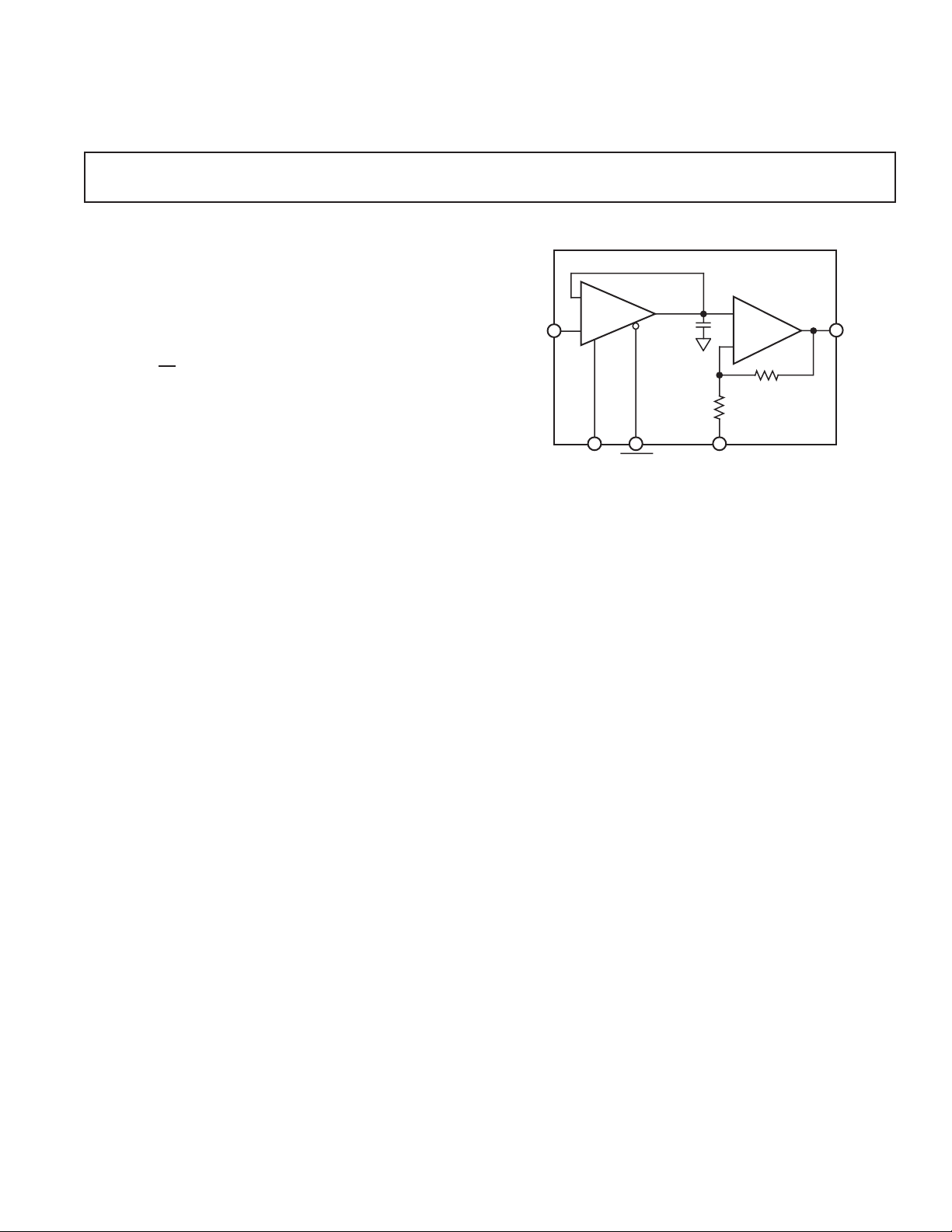
Sampling Amplifier
AD9101
FEATURES
350 MHz Sampling Bandwidth
125 MHz Sampling Rate
Excellent Hold Mode Distortion
–75 dB @ 50 MSPS (25 MHz V
–57 dB @ 125 MSPS (50 MHz V
7 ns Acquisition Time to 0.1%
<1 ps Aperture Jitter
66 dB Feedthrough Rejection @ 50 MHz
3.3 nV/√ APPLICATIONS
Direct IF Sampling
Digital Sampling Oscilloscopes
HDTV Cameras
Peak Detectors
Radar/EW/ECM
Spectrum Analysis
Test Equipment/CCD Testers
DDS DAC Deglitcher
Hz Spectral Noise Density
)
IN
)
IN
The benefits of using a track-and-hold ahead of a flash converter
have been well known for many years. However, before the
AD9101, there was no track-and-hold amplifier with sufficient
GENERAL DESCRIPTION
The AD9101 is an extremely accurate, general purpose, high
speed sampling amplifier. Its fast and accurate acquisition speed
allows for a wide range of frequency vs. resolution performance.
The AD9101 is capable of 8 to 12 bits of accuracy at clock rates
of 125 MSPS or 50 MSPS, respectively. This level of performance makes it an ideal driver for almost all 8- to 12-bit A/D
encoders on the market today.
In effect, the AD9101 is a track-and-hold with a post amplifier.
This configuration allows the front end sampler to operate at
relatively low signal amplitudes. This results in dramatic improvement in both track and hold mode distortion while keeping
power low.
The gain-of-four output amplifier has been optimized for fast
and accurate large signal step settling characteristics even when
heavily loaded. This amplifier’s fast Settling Time Linearity
(STL) characteristic causes the amplifier to be transparent to
the low signal level distortion of the sampler. When sampled,
output distortion levels reflect only the distortion performance
of the sampler.
Dramatic SNR and distortion improvements can be realized
when using the AD9101 with high speed flash converters. Flash
bandwidth and linearity to markedly increase the dynamic performance of such flashes as the AD9002, AD9012, AD9020,
and AD9060.
A new application made possible by the AD9101 is direct IFto-digital conversion. Using the Nyquist principle, the IF
frequency can be rejected and the baseband signal can be
recovered. As an example, a 40 MHz IF is modulated by a
10 MHz bandwidth signal. By sampling at 25 MSPS, the signal
of interest is detected.
The AD9101 is offered in commercial and military temperature
ranges. Commercial versions include the AD9101AR in plastic
SOIC and AD9101AE in ceramic LCC. Military devices are
available in ceramic LCC. Contact the factory for availability of
versions in DIP and/or military versions.
PRODUCT HIGHLIGHTS
1. Guaranteed Hold-Mode Distortion
2. 125 MHz Sampling Rate to 8 Bits; 50 MHz to 12 Bits
3. 350 MHz Sampling Bandwidth
4. Super-Nyquist Sampling Capability
5. Output Offset Adjustable
converters generally have excellent linearity at dc and low frequencies. However, as signal slew rate increases, their performance degrades due to the internal comparators’ aperture delay
variations and finite gain bandwidth product.
REV. 0
Information furnished by Analog Devices is believed to be accurate and
reliable. However, no responsibility is assumed by Analog Devices for its
use, nor for any infringements of patents or other rights of third parties
which may result from its use. No license is granted by implication or
otherwise under any patent or patent rights of Analog Devices.
One Technology Way, P.O. Box 9106, Norwood, MA 02062-9106, U.S.A.
Tel: 617/329-4700 World Wide Web Site: http://www.analog.com
Fax: 617/326-8703 © Analog Devices, Inc., 1997
FUNCTIONAL BLOCK DIAGRAM
Page 2

AD9101–SPECIFICA TIONS
ELECTRICAL CHARACTERISTICS
(+VS = +5 V, –VS = –5.2 V, R
= 100 V, RlN = 50 V unless otherwise noted)
LOAD
Test AD9101
Parameter Conditions Temp Level Min Typ Max Units
DC ACCURACY
Gain ∆V
Offset V
= 0.5 V 25°C I 3.93 4 4.07 V/V
IN
∆V
= 0.5 V Full VI 3.9 4.1 V/V
IN
= 0 V 25°CI ±3±10 mV
IN
V
= 0 V Full VI ±15 mV
IN
Output Resistance 25°C V 0.4 Ω
Output Drive Capability Full VI ±60 ± 70 mA
PSRR ∆V
Pedestal Sensitivity to Positive Supply ∆V
= 0.5 V p-p 25°CVI3743 dB
S
= 0.5 V p-p Full V 4 mV/V
S
Pedestal Sensitivity to Negative Supply ∆VS = 0.5 V p-p Full V 8 mV/V
ANALOG INPUT/OUTPUT
Output Voltage Range Full VI ±2.4 ±2.7 V
Input Bias Current 25°CI ±5±15 µA
Full VI ±20 µA
Input Capacitance 25°CV 2 pF
Input Resistance 25°C–T
T
MIN
CLOCK/
CLOCK INPUTS
Input Bias Current CL/
Input Low Voltage (V
Input High Voltage (VIH)
1
)
IL
1
VIN = 0.5 V p-p Full VI –1.8 –1.5 V
VIN = 0.5 V p-p Full VI –1.0 –0.8 V
CL = –1.0 V Full VI 3 3.6 mA
VI 30 125 kΩ
MAX
VI 25 kΩ
TRACK MODE DYNAMICS
Bandwidth (–3 dB) V
Slew Rate 4 Volt Output Step Full IV 1300 1800 V/µs
Overdrive Recovery Time
2
(to 0.1%) VIN = ±1 V to 0 V 25°CV 55 ns
= 1 V p-p Full IV 160 250 MHz
OUT
Integrated Output Noise (5 MHz–200 MHz) 25°C V 210 µV
Input RMS Spectral Noise @ 10 MHz 25°C V 3.3 µV/√Hz
HOLD MODE DYNAMICS
Worst Harmonic (23 MHz, 50 MSPS) V
Worst Harmonic (48 MHz, 100 MSPS) V
Worst Harmonic (48 MHz, 100 MSPS) V
Worst Harmonic (48 MHz, 100 MSPS) V
Worst Harmonic (48 MHz, 125 MSPS) V
Sampling Bandwidth (–3 dB)
Hold Noise
4
(RMS) Full V 150 × t
3
= 2 V p-p 25°C V –75 dBFS
OUT
= 2 V p-p 25°C IV –62 –57 dBFS
OUT
= 2 V p-p Full (Ind.) IV –53 dBFS
OUT
= 2 V p-p Full (Mil.) IV –51 dBFS
OUT
= 2 V p-p 25°C V –57 dBFS
OUT
VIN = 0.5 V p-p 25°C V 350 MHz
H
mV/s
Droop Rate 25°CI ±5±18 mV/µs
Full VI ±40 mV/µs
Feedthrough Rejection (50 MHz) V
= 2 V p-p Full V –66 dB
OUT
TRACK-TO-HOLD SWITCHING
Aperture Delay 25°C V –250 ps
Aperture Jitter 25°C V <1 ps rms
Pedestal Offset V
Transient Amplitude V
Settling Time to 4 mV V
Glitch Product
5
= 0 V 25°CI ±5±20 mV
IN
V
= 0 V Full VI ±35 mV
IN
= 0 V Full V 8 mV
IN
= 0 V Full V 4 ns
IN
VIN = 0 V 25°C V 20 pV-s
HOLD-TO-TRACK SWITCHING
Acquisition Time to 0.1% 2 V Output Step 25°CV 7 ns
Acquisition Time to 0.01% 2 V Output Step 25°CIV 1114ns
2 V Output Step Full IV 16 ns
POWER SUPPLY
+V
Current Full VI 55 70 mA
S
–V
Current Full VI 59 73 mA
S
Power Dissipation Full VI 570 715 mW
–2–
REV. 0
Page 3
AD9101
T
NOTES
1
If the analog input exceeds ±300 mV, the clock levels should be shifted as shown in the Theory of Operation section entitled “Driving the Encode Clock.”
2
Time to recover within rated error band from 160% overdrive.
3
Sampling bandwidth is defined as the –3 dB frequency response of the input sampler to the hold capacitor when operating in the sampling mode. It is greater than
tracking bandwidth because it does not include the bandwidth of the output amplifier.
4
Hold mode noise is proportional to the length of time a signal is held. For example, if the hold time (t
(150 mV/s × 20 ns). This value must be combined with the track mode noise to obtain total noise.
5
Total energy of worst case track-to-hold or hold-to-track glitch.
Specifications subject to change without notice.
ABSOLUTE MAXIMUM RATINGS
Supply Voltage (+VS) . . . . . . . . . . . . . . . . . . . . –0.5 V to +6 V
Supply Voltage (–V
) . . . . . . . . . . . . . . . . . . . . –6 V to +0.5 V
S
Analog Input Voltage . . . . . . . . . . . . . . . . . . . . . . . . . . . . ±5 V
CLOCK/
Continuous Output Current
CLOCK Input . . . . . . . . . . . . . . . . . –5 V to +0.5 V
4
. . . . . . . . . . . . . . . . . . . . 70 mA
Storage Temperature . . . . . . . . . . . . . . . . . . –65°C to +150°C
Operating Temperature Range
AE, AR . . . . . . . . . . . . . . . . . . . . . . . . . . . . –40°C to +85°C
SE . . . . . . . . . . . . . . . . . . . . . . . . . . . . . . –55°C to +125°C
Junction Temperature (Ceramic)
Junction Temperature (Plastic)
Soldering Temperature (1 minute)
NOTES
1
Absolute maximum ratings are limiting values to be applied individually, and
beyond which the serviceability of the circuit may be impaired. Functional
operability is not necessarily implied. Exposure to absolute maximum rating
conditions for an extended period of time may affect device reliability.
2
Typical thermal impedances (no air flow, soldered to PC board) are as follows:
Ceramic LCC: θJA = 48°C/W; θJC = 9.9°C/W; Plastic SOIC: θJA = 54°C/W;
θ
= 7.3°C/W.
JC
3
For surface mount devices, mounted by vapor phase soldering. Prior to vapor phase
soldering, plastic units should receive a minimum eight hour bakeout at 110°C to
drive off any moisture absorbed in plastic during shipping or storage. Through-hole
devices can be soldered at +300°C for 10 seconds.
4
Output is short circuit protected to ground. Continuous short circuit may affect
device reliability.
1
2
. . . . . . . . . . . . . . . +175°C
2
. . . . . . . . . . . . . . . . +150°C
3
. . . . . . . . . . . . . . +220°C
Pin Description
Pin Description Connection
1 RTN Gain Set Resistor Return*
2 RTN Gain Set Resistor Return*
3C
4+V
5+V
6 GND Hold Capacitor Ground
7 GND Hold Capacitor Ground
8+V
9+V
10 CLK True ECL T/H Clock
11
12 –V
13 –V
14 N/C No Connection
15 V
16 GND Ground (Signal Return)
17 –V
18 –V
19 C
20 V
*See “Matching the AD9101 to A/D Encoders.” Both pins should be either
grounded or connected to voltage source for offset.
EXPLANATION OF TEST LEVELS
Test Level
I – 100% production tested.
II – 100% production tested at +25°C, and sample tested at
specified temperatures.
III – Periodically sample tested.
IV – Parameter is guaranteed by design and characterization
testing.
V – Parameter is a typical value only.
VI – All devices are 100% production tested at +25°C. 100%
production tested at temperature extremes for extended
temperature devices; sample tested at temperature
extremes for commercial/industrial devices.
ORDERING INFORMATION
Temperature Package Package
Model Range Description Option
RTN
RTN
C
+V
+V
GND
GND
+V
+V
CLK
B+
AD9101AR –40°C to +85°C Plastic SOIC R-20
AD9101AE –40 °C to +85°C LCC E-20A
AD9101SE –55 °C to +125°C LCC E-20A
CAUTION
ESD (electrostatic discharge) sensitive device. Electrostatic charges as high as 4000 V readily
accumulate on the human body and test equipment and can discharge without detection.
Although the AD9101 features proprietary ESD protection circuitry, permanent damage may
occur on devices subjected to high energy electrostatic discharges. Therefore, proper ESD
precautions are recommended to avoid performance degradation or loss of functionality.
) is 20 ns, the accumulated noise is typically 3 µV
H
B+
S
S
S
S
Bootstrap Capacitor (Positive Bias)
+5 V Power Supply (Analog)
+5 V Power Supply (Analog)
+5 V Power Supply (Digital)
+5 V Power Supply (Digital)
CLK Complement ECL T/H Clock
S
S
IN
S
S
B–
OUT
–5.2 V Power Supply (Digital)
–5.2 V Power Supply (Digital)
Analog Signal Input
–5.2 V Power Supply (Analog)
–5.2 V Power Supply (Analog)
Bootstrap Capacitor (Negative Bias)
Analog Signal Output
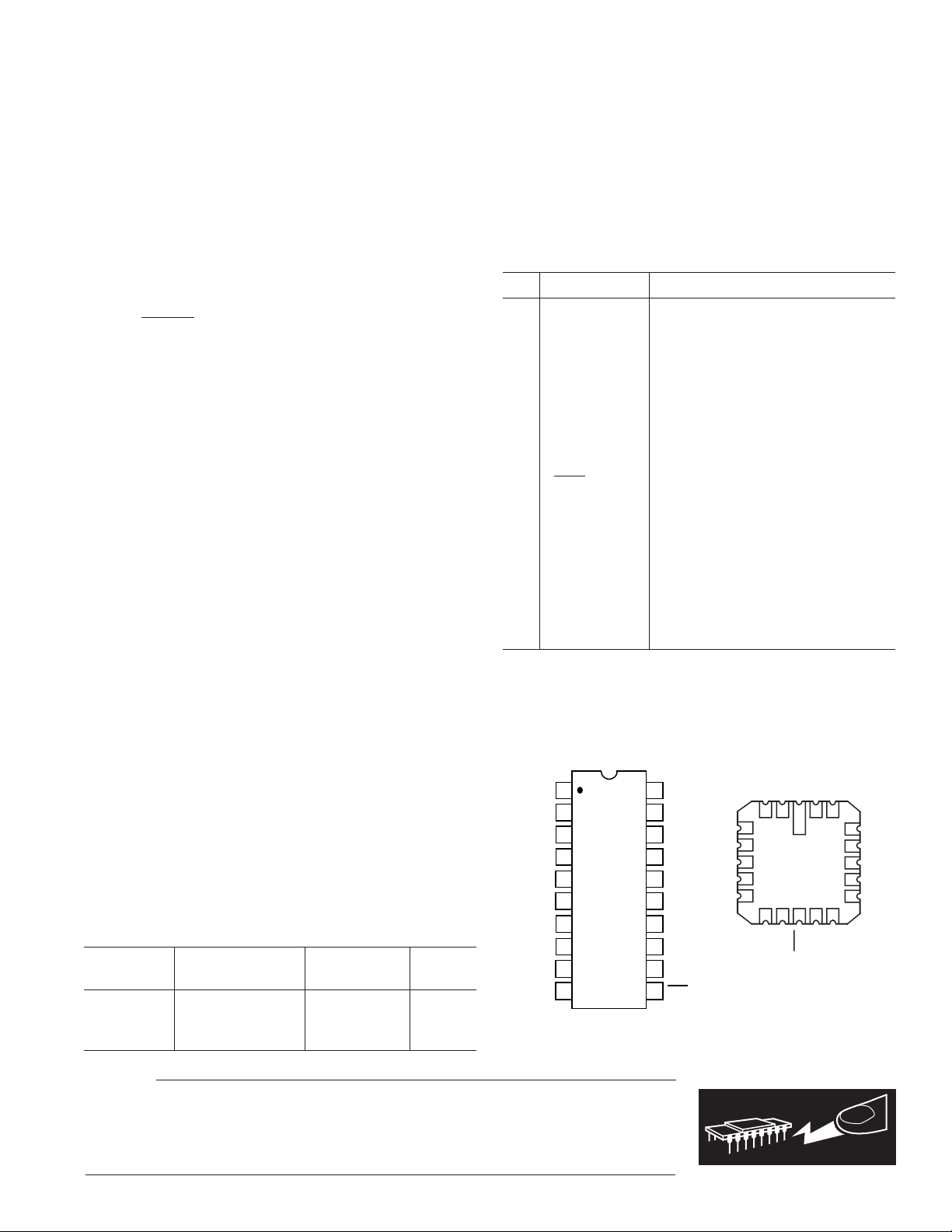
PIN CONFIGURATIONS
20-Pin SOIC
1
2
3
4
S
AD9101
5
S
TOP VIEW
(Not to Scale)
6
7
8
S
9
S
10
V
20
C
19
–V
18
–V
17
GND
16
15
V
14
NC
–V
13
–V
12
11
CLK
20-Contact Ceramic LCC
OU
B–
V
S
S
IN
C
19
18
17
16
BOTTOM VIEW
15
14
13
S
–V
20
S
–V
OUT
B–
IN
–V
S
–V
S
GND
V
NC
S
S
1112
1
RTN
23
CLK
RTN
CLK
WARNING!
ESD SENSITIVE DEVICE
B+
C
4
5
6
7
8
910
S
+V
+V
+V
GND
GND
+V
S
S
S
REV. 0
–3–
Page 4

AD9101
Acquisition Time is the amount of time it takes the AD9101
to reacquire the analog input when switching from hold to track
mode. The interval starts at the 50% clock transition point and
ends when the input signal is reacquired to within a specified
error band at the hold capacitor.
Aperture Delay establishes when the input signal is actually
sampled. It is the time difference between the analog propagation delay of the front-end buffer and the control switch delay
time (the time from the hold command transition to when the
switch is opened). For the AD9101, this is a negative value,
meaning that the analog delay is longer than the switch delay.
Aperture Jitter is the random variation in the aperture delay.
This is measured in ps-rms and is manifested as phase noise on
the held signal.
Droop Rate is the change in output voltage as a function of
time (dV/dt). It is measured at the AD9101 output with the device in hold mode and the input held at a specified dc value; the
measurement starts immediately after the T/H switches from
track to hold.
Feedthrough Rejection is the ratio of the output signal to the
input signal when in hold mode. This is a measure of how well
the switch isolates the input signal from feeding through to the
output.
+2V
Hold-to-Track Switch Delay is the time delay from the track
command to the point when the output starts to change to acquire a new signal level.
Pedestal Offset is the offset voltage measured immediately after the AD9101 is switched from track to hold with the input
held at zero volts. It manifests itself as a dc offset during the
hold time.
Sampling Bandwidth is the –3 dB frequency response from
the input to the hold capacitor under sampling conditions. It is
greater than the tracking bandwidth because it does not include
the bandwidth of the output amplifier which is optimized for
settling time rather than bandwidth.
Track-to-Hold Settling Time is the time necessary for the
track to hold switching transient to settle to within 4 mV of its
final value.
Track-to-Hold Switching Transient is the maximum peak
switch induced transient voltage which appears at the AD9101
output when it is switched from track to hold.
APERTURE
DELAY
(–0.25 ns)
ANALOG
INPUT (x 4)
SAMPLER OUTPUT SIGNAL (x 4)
AND AMPLIFIER OUTPUT SIGNAL
CLOCK
INPUTS
0V
-2V
+2V
0V
-2V
"1"
"0"
ACQUISITION
TIME (SEE
TEXT)
HOLD TO TRACK
SWITCH DELAY
TIME (1.5 ns)
CLOCK
"HOLD"
Timing Diagram (500 ps/div)
VOLTAGE
LEVEL HELD
OBSERVED AT
HOLD CAPACITOR
OBSERVED AT
AMPLIFIER OUTPUT
CLOCK
"TRACK"
TRACK TO
HOLD
SETTLING
(4 ns)
"HOLD"
CLOCK
–4–
REV. 0
Page 5

AD9101
THEORY OF OPERATION
The AD9101 employs a new and unique track-and-hold architecture. Previous commercially available high speed track-andholds used an open loop input buffer, followed by a diode
bridge, hold capacitor and output buffer (closed or open loop)
with an FET device usually connected to the hold capacitor.
This architecture required mixed device technology and, usually, hybrid construction. The sampling rate of these hybrids has
been limited to 20 MSPS for 12-bit accuracy. Distortion generated in the front-end amplifier/bridge limited the dynamic range
performance to the “mid –70 dBFS” for analog input signals of
less than 10 MHz. Broadband and switch-generated noise limited the SNR of previous track-and-holds to about 70 dB.
The AD9101 is a monolithic device using a high frequency
complementary bipolar process to achieve new levels of high
speed precision. Its architecture completely breaks from the traditional architecture described above. The hold switch has been
integrated into the first stage closed-loop buffer. This innovation provides error (distortion) correction for both the switch
and buffer while still achieving slew rates representative of an
open-loop design. In addition, acquisition slew current for the
hold capacitor is higher than the traditional diode bridge switch
configurations, removing a main contributor to the limits of
maximum sampling rate, input frequency and distortion.
The closed-loop output amplifier includes zero voltage bias current cancellation, which results in high-temperature droop rates
close to those found in FET type inputs. This closed-loop amplifier inherently provides high speed loop correction and has
extremely low distortion even when heavily loaded.
Extremely fast time constant linearity (7 ns to 0.01% for a 4 V
output step) ensures that the output amplifier does not limit the
AD9101 sampling rate or analog input frequency. (The acquisition and settling time are primarily limited only by the input
sampler.) The output is transparent to the overall AD9101 hold
mode distortion levels for loads as low as 50 Ω.
Full-scale track and acquisition slew rates achieved by the
AD9101 are 1800 V/µs and 1700 V/µs, respectively. When com-
bined with excellent phase margin (typically 5% overshoot),
wide bandwidth, and dc gain accuracy, acquisition time to
0.01% is only 11 ns.
Acquisition Time
Acquisition time is the amount of time it takes the AD9101 to
reacquire the analog input when switching from hold-to-track
mode. The interval starts at the 50% clock transition point and
ends when the input signal is reacquired to within a specified error band at the hold capacitor.
The hold-to-track switch delay (t
) cannot be subtracted
DHT
from this acquisition time for 12-bit performance because it is a
charging time and analog output delay that occurs when moving
from hold to track; this delay is typically 1.5 ns. Therefore, the
track time required for the AD9101 is the acquisition time
which includes t
. Note that the acquisition time is defined as
DHT
the settled voltage at the hold capacitor and does not include the
delay and settling time of the output amplifier. The example in
Figure 1 illustrates why the output amplifier does not contribute
to the overall acquisition time.
The exaggerated illustration in Figure 1 shows that V
settled to within x% of its final value, but V
(due to slew rate
OUT
HC
has
limitations, finite BW, power supply ringing, etc.) has not settled
V
SAMPLER
V
HC
V
OUT
t
DHT
1.5ns
HC
HC
TRACK
AMP
TRACK-TO-HOLD
INDUCED GLITCH
ACQUISITION TIME
AT HC TO X%
TS
HOLD
V
OUT
Figure 1. Acquisition Time at Hold Capacitor
during the track time. However, since the output amplifier always “tracks” the front end circuitry, it “catches up” and directly superimposes itself (less about 500 ps of analog delay) to
V
. Since the small signal settling time of the output amplifier
HC
can be about 1.2 ns to ±1 mV, and is significantly less than the
hold time, acquisition time should be referenced to the hold
capacitor.
Most of the hold settling time and output acquisition time are
due to the sampler and the switch network. (Output acquisition
time is as seen on a scope at the output. This is typically 1.7 ns
longer than actual acquisition time.) For track time, the output
amplifier contributes only about 5 ns of the total; in hold mode,
it contributes 1.7 ns (as stated above).
A stricter definition of acquisition would actually include both
the acquisition and track-to-hold settling times to a defined accuracy. To obtain 12-bit+ distortion levels and 50 MSPS operation, the minimum recommended track and hold times are
12 ns and 8 ns, respectively. To drive an 8-bit flash converter
(such as the AD9002) with a 2 V p-p full-scale input, hold time
to 1 LSB accuracy will be limited primarily by the aperture time
of the encoder, rather than by the AD9101. This makes it possible to reduce track time to as little as 5 ns, with hold time chosen to optimize the encoder’s performance.
Though acquisition time and track-to-hold settling time to
1/2 LSB (0.4%) accuracy are 6 ns and 4 ns respectively, it is still
possible to achieve –45 dB SNR performance at clock speeds to
125 MSPS. This is because the settling error is roughly proportional to the signal level and is partially cancelled due to the
high phase margin of the input sampler.
Hold vs. Track Mode Distortion
In many traditional high speed, open-loop track-and-holds,
track mode distortion is often much better than hold mode distortion. Track mode distortion does not include nonlinearities
due to the switch network, and does not correlate to the relevant
hold mode distortion. But since hold mode distortion has traditionally been omitted from manufacturer’s specification tables,
users have had to discover for themselves the effective overall
hold mode distortion of the combined T/H and encoder.
REV. 0
–5–
Page 6

AD9101
The architecture of the AD9101 minimizes hold mode distortion over its specified frequency range. As an example, in track
mode the worst harmonic generated for a 20 MHz input tone is
typically –65 dBFS. In hold mode, under the same conditions
and sampling at 50 MSPS, the worst harmonic generated is
–75 dBFS. The reason is the output amplifier in hold mode has
only a dc distortion relevancy. With its inherent linearity (7 ns
settling to 0.01%), the output amplifier has essentially settled to
its dc distortion level even for track plus hold times as short as
20 ns. For a traditional open-loop output buffer, the ac (track
mode) and dc (hold mode) distortion levels are often the same.
Droop Rate
Droop rate does not necessarily affect a track-and-hold’s distortion characteristics. If the droop rate is constant versus the input
voltage for a given hold time, it manifests itself as a dc offset
to the encoder. For the AD9101, the droop rate is typically
3 mV/µs. If a signal is held for 1 µs, a subsequent encoder will
see a 3 mV offset voltage. If there is no droop sensitivity to the
held voltage value, the offset would be constant and “ride” on
the input signal and introduce no hold-mode nonlinearities.
When droop rate varies proportionately to the level of the held
voltage signal level, only a gain error is introduced to the A/D
encoder. The AD9101 has a droop sensitivity to the input level
of 20 mV/V µs. For a 2 V p-p output signal, this translates to a
1%/µs gain error and does not cause additional distortion errors.
However, hold times longer than about 500 ns can cause distortion due to the R × HC time constant at the hold capacitor. In
addition, hold mode noise will increase linearly vs. hold time
and thus degrade SNR performance.
Layout Considerations
For best performance results, good high speed design techniques must be applied. The component (top) side ground
plane should be as large as possible; two-ounce copper cladding
is preferable. All runs should be as short as possible, and decoupling capacitors must be used.
The schematic of a recommended AD9101 evaluation board is
shown. (Contact factory concerning availability of assembled
boards.) All 0.01 µF decoupling capacitors should be low induc-
tance surface mount devices (P/N 05085C103MT050 from
AVX) and connected with short lead lengths to minimize stray
inductance.
The 10 µF, low frequency tantalum power supply decoupling
capacitors should be located within 1.5 inches of the AD9101.
The common 0.01 µF supply capacitors can be wired together.
The common power supply bus (connected to the 10 µF capaci-
tor and power supply source) can be routed to the underside of
the board to the daisy chain wired 0.01 µF supply capacitors.
For remote input and/or output drive applications, controlled
impedances are required to minimize line reflections that will
reduce signal fidelity. When capacitive and/or high impedance
levels are present, the load and/or source should be physically
located within approximately one inch of the AD9101. Note
that a series resistance, R
6 pF. (The Recommended R
formance Section” shows values of R
, is required if the load is greater than
S
vs. CL chart in the “Typical Per-
S
for various capacitive
S
loads which result in no more than a 20% increase in settling
time for loads up to 80 pF.) For best results when driving
heavily capacitive or low resistance loads, the AD9630 buffer is
strongly suggested. As much of the ground plane as possible
should be removed from around the VIN and V
pins to mini-
OUT
mize coupling onto the analog signal path.
While a single ground plane is recommended, the analog signal
and differential ECL clock ground currents follow a narrow path
directly under their common voltage signal line. To reduce reflections, especially when terminations are used for transmission
line efficiency, the clock, V
and V
IN
signals and respective
OUT
ground paths should not cross each other; if they do, unwanted
coupling can result. Analog terminations should be kept as far as
possible from the power supply decoupling capacitors to minimize supply current spike feedthrough.
Driving the Encode Clock
The AD9101 requires a differential ECL clock command. Due
to the high gain bandwidth of the AD9101 internal switch, the
input clock should have a slew rate of at least 400 V/µs.
To obtain maximum signal to noise performance, especially at
high analog input frequencies, a low jitter clock source is required. The AD9101 clock can be driven by an AD96685, an
ultrahigh speed ECL comparator with very low jitter.
Figure 2 illustrates a recommended termination for the differential encode clock inputs of the AD9101. The 40 Ω R
LS
is required to level shift the ECL voltages more negative. This
increases the linear signal range of the sampler. When the input
is less than 600 mV (2.4 V p-p output), these level shift resistors
are not required.
–5.2 V
510
R
LS
40
R
LS
40
510
–5.2 V
CLK
10
CLK
11
Figure 2. Recommended Encode Clock Termination
When driving the encode clock from a remote circuit via
transmission lines, or where stray capacitance exceeds 2 pF,
Thevenin equivalent terminations should be used (270 Ω to
–5.2 V and 160 Ω to ground). For this 100 Ω equivalent termination, R
Driving the Analog Input
should be 20 Ω.
LS
Special care must be taken to ensure that the analog input signal
is not compromised before it reaches the AD9101. To obtain
maximum signal to noise performance, a very low phase noise
analog source is required. In addition, input filtering and/or a
low harmonic signal source is necessary to maximize the spurious free dynamic range. Any required filtering should be located
close to the AD9101 and away from digital lines.
Matching the AD9101 to A/D Encoders
The AD9101’s analog output level may have to be offset or amplified to match the full-scale range of a given A/D converter.
This can generally be accomplished by inserting an amplifier after the AD9101. For example, the AD671 is a 12-bit 500 ns
monolithic ADC encoder that requires a 0 V to +5 V full-scale
analog input. An AD84X series amplifier could be used to condition the AD9101 output to match the full-scale range of the
AD671.
The AD9101 can perform a dc level shift function when its input
is bipolar and the ADC requires a unipolar signal. The AD9002
–6–
REV. 0
Page 7

provides a good example. It operates on a single negative supply
–70
–50
–30
1 10 100
–45
–40
–35
–55
–60
–65
dB
MHz
WITH AD9101
ENCODE = 125 MSPS
WORST HARMONIC
SNR W/HARMONICS
WITH AD9101
with the input range from 0 V to –2 V. By connecting Pins 1
and 2 (RTN) to a +0.33 V level, rather than its usual ground
connection, a bipolar ±0.25 V input is shifted to 0 V to –2 V at
the AD9101’s output (see Figure 3 in the Applications section.)
APPLICATIONS
Because of its rapid acquisition and low distortion, the AD9101
is useful in a wide range of signal processing.
Choosing Between the AD9100 and AD9101
The first obvious difference between the AD9100 and AD9101
is sample rate. Simplistically, any high resolution system (12–16
bits) operating below 25 MSPS will use the AD9100 and 8–12
bit systems operating above 25 MSPS will use the AD9101.
There are, however, some subtle characteristics of these high
performance track-and-hold amplifiers that create some exceptions to these guidelines. The typical curve entitled “Dynamic
Range vs. Analog Frequency” should be considered when
choosing between these two high performance track-and-holds.
When speed is critical, the AD9101 should receive strong consideration, even in high resolution systems. Using a reduced signal amplitude through the AD9100 greatly reduces slew limiting
effects and should also be considered when converting high frequency (up to 70 MHz) analog signals with encode rates below
25 MSPS.
Sampler for Flash ADC
Flash ADCs typically suffer degradation of dynamic range as
signal frequency increases. The AD9101 was designed specifically for the purpose of boosting this performance and allowing
users to obtain maximum performance with flash ADCs. Figure
3 shows the block diagram and timing relationship for an 8-bit,
125 MSPS converter.
+5V
1k
3k
1k
0.33V
+
–
0.1µF
RTN
AC
AD9101
40Ω
AD9002
AD9101
Figure 4. AD9002 Dynamic Range With and Without
AD9101
27Ω
8.5 ns
"TRACK"
"HOLD"
CLOCK 1
2.5 ns
CLOCK 2
AD9101
CLOCK 1
8.5 ns
"TRACK"
"HOLD"
8.25 ns
AD9630
"HOLD"
8 ns
8.25 ns 8.25 ns 8.25 ns
"TRACK"
Figure 5. AD9101 with 10-Bit, 75 MSPS ADC
–70
–65
–60
–55
WITH AD9101
WITH AD9101
"HOLD"
8 ns
"TRACK"
AD9060
CLOCK 2
8.5 ns
"TRACK"
"HOLD"
8.25 ns
WORST
HARMONIC
SNR W/
HARMONICS
HOLD
CLOCK 1
(AD9101)
1.6 ns
CLOCK 2
(AD9002)
Figure 3. AD9101 with 8-Bit, 125 MSPS Flash
Figure 4 contrasts performance of the flash converter alone vs.
the circuit of Figure 3.
Figures 5 and 6 show the block diagrams and dynamic range
improvement when the AD9101 is used ahead of an 10-bit, 75
MSPS flash converter. The AD9630 is not required if the input
frequency is limited to 40 MHz.
REV. 0
3.6 ns
TRACK
4.4 ns
HOLD
3.5 ns
4.5 ns
TRACK
CLOCK 1 CLOCK 2
HOLD
3.6 ns
TRACK
44 ns
HOLD
3.5 ns
3.6 ns
TRACK
HOLD
4.5 ns
TRACK
3.5 ns
–50
dB
–45
–40
ENCODE = 60 MSPS
–35
–30
1 10 100
MHz
Figure 6. AD9060 Dynamic Performance With and Without AD9101
–7–
Page 8

AD9101
Deglitcher
Many recently announced video-speed digital-to-analog converters feature very low glitch impulse. This is the result of design emphasis on spurious free dynamic range (SFDR), a key
spec for the emerging direct digital synthesis (DDS) market.
These DACs have extremely low spurs and often do not require
deglitching.
Although their specs are impressive, these DACs may suffer harmonic distortion, especially at higher clock rates. Therefore, a
deglitcher using the AD9101 can improve SFDR in some cases.
Figure 7 illustrates the block diagram for deglitching an
AD9713, 12-bit DAC.
TUNING
WORD
32
DDS
ACCUMULATOR
(AD9955)
CLK1
12
DAC
(AD9713)
CLK2 CLK3
SAMPLING
AMPLIFIER
(AD9101)
LOW
DISTORTION
OUTPUT
Figure 7. Deglitcher Block Diagram
IF-to-Digital Conversion
Traditional receivers with information encoded with in phase (I)
and quadrature (Q) signals comprise extensive analog signal
processing ahead of the pair of ADCs.
This I-Q demodulation in the analog domain requires precise
gain and phase matching as well as close matching of the ADCs.
This leads to high cost both in materials and labor to attain the
desired performance. Digital front end designers have paid the
cost for these components because ADCs have limited the dynamic range at higher signal frequencies.
Thus, the final IF signal was mixed with quadrature signals
from the final LO. The two resultant baseband signals representing I and Q were digitized by independent converters.
Q
ADC
90°
ANALOG
INPUT
IF
BPF
LOCAL
OSC.
QUADRATURE
DEMODULATOR
WITH GAIN
MATCHED LPF
ADC
ADCs
BASEBAND
I
DSP
Figure 8. Traditional l-Q Demodulation
This method, shown in block form in Figure 8, relies heavily on
accuracy of the phase of the analog I and Q signals applied to
the ADCs. As little as 0.5° of phase error can reduce system dynamic range by 6 dB or more.
Using the bandwidth and low distortion of the AD9101 greatly
simplifies the analog front end and allows signal processing to
be done in the digital domain which is more predictable and less
susceptible to environmental changes. The simplified front end
is illustrated in Figure 9.
This configuration removes the burden from the analog section.
The AD9101 expands the dynamic range of the ADC into the
IF bandwidth, allowing straightforward digital algorithms to demodulate the I and Q data.
ANALOG
INPUT
IF
BPF
NUMERICALLY
AD9101
ADC
12
Figure 9. Direct IF-to-Digital
CONTROLLED
OSCILLATOR
(NCO)
H (z)
H (z)
Q
FILTER
DIGITAL
DSP
I
–8–
REV. 0
Page 9

J1
V
IN
CLOCK
INPUT
10 µF
AD9101
V
NC
Q
–V
S
C6
10 µF
+
V
OUT
20
19
B–
18
S
17
S
16
15
IN
14
13
S
12
S
11
R1
27
C7
C8
H2
+5V
AD9101
EVALUATION
BOARD
3.5 (88.9)
J2
CLOCK IN
H1 H4
C2
R4 C4
R3
C3
3.0 (76.2)
GND
C1
OUT
C5
C9
U1
–5.2V
C6
R1
C9
C7
R5
R7
H3
J3
V
OUT
R2
J1
V
IN
AD9101 Layout
R6,160
R4,160
R7, 270
R5, 270
–5.2 V
+V
S
+
C2
1
2
3
C3
4
5
6
7
8
C4
9
10
R2
51
J2
R3
51
3
4
RTN
RTN
AD9101
C
B+
+V
S
+V
S
GND
GND
+V
S
+V
S
CLK
U1
AD96685BR
+
–
6
C1
V
OUT
C
–V
–V
GND
–V
–V
CLK
11
Q
12
LE
NOTES
1. ALL CAPACITORS ARE 0.01 mF UNLESS OTHERWISE
DESIGNATED. SURFACE-MOUNT CAPS PREFERRED.
2. R1 SHOULD BE SELECTED BASED ON CL AND MAY BE
SHORTED FOR CAPACITIVE LOADS OF LESS THAN 6 pF.
3. C1 SHOULD HAVE A LOW INDUCTANCE 0.01 mF WITH
CIRCUIT LEADS AS SHORT AS POSSIBLE.
4. PINOUTS FOR AD9101 AND AD96685 ARE FOR SOIC.
Evaluation Circuit
EVALUATION BOARD ORDERING GUIDE
Part Number Description
AD9101/PCB Fully Populated and Tested Evaluation Board
AD9101/PWB Printed Circuit Board without Components
Component Side
REV. 0
Ground Plane Bottom
–9–
Page 10

AD9101 – Typical Performance Curves
Gain vs. Frequency (Track Mode)
Track-to-Hold-to-Track Transients
Hold Mode Distortion vs. Analog
Input Frequency
Feedthrough vs. Input Frequency
Recommended RS vs. CL for Optimal
Settling Time
Droop Rate vs. Temperature
Settling Tolerance vs. Acquisition
Time
–10–
Power Supply Rejection Ratio vs.
Frequency
REV. 0
Page 11

OUTLINE DIMENSIONS
Dimensions are shown in inches and (mm).
AD9101
0.0125 (0.32)
0.0091 (0.23)
20
1
0.50 (1.27) BSC
20-Pin SOIC
0.512 (13.00)
0.496 (12.60)
TOP VIEW
0.019 (0.49)
0.014 (0.35)
11
0.299 (7.60)
0.291 (7.40)
10
0.012 (0.30)
0.004 (0.10)
0.050 (1.27)
0.016 (0.40)
0.419 (10.65)
0.394 (10.00)
0.104 (2.65)
0.093 (2.35)
0.055 (1.40)
0.045 (1.14)
18
17
16
15
14
20-Contact LCC
1232019
NO. 1 PIN
INDEX
BOTTOM VIEW
13
12 11 10 9
0.358 (9.09)
0.342 (8.69)
4
5
6
7
8
0.075
(1.91)
REF.
0.028 (0.71)
0.022 (0.56)
0.050
(1.27)
BSC
0.100 (2.54)
0.064 (1.63)
REV. 0
–11–
Page 12

C1659–24–5/92
PRINTED IN U.S.A.
 Loading...