

Page 1
10-Bit, 100 MSPS
a
FEATURES
10-Bit, 100 MSPS ADC
Low Power: 450 mW at 100 MSPS
On-Chip Track/Hold
280 MHz Analog Bandwidth
SINAD = 54 dB @ 41 MHz
On-Chip Reference
1 V p-p Analog Input Range
Single 5 V Supply Operation
5 V/3.3 V Outputs
APPLICATIONS
Digital Communications
Signal Intelligence
Digital Oscilloscopes
Spectrum Analyzers
Medical Imaging
Sonar
HDTV
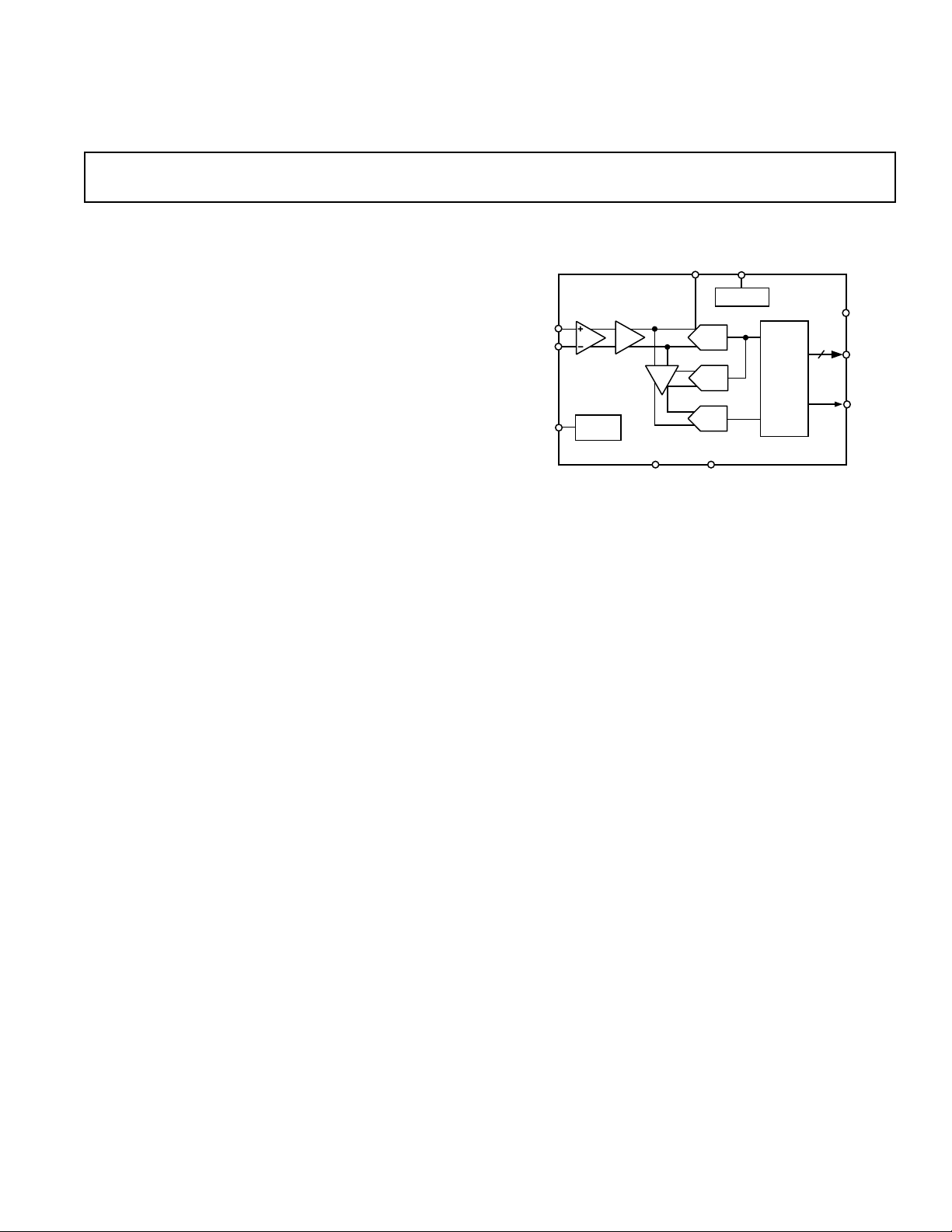
GENERAL DESCRIPTION
The AD9071 is a monolithic sampling analog-to-digital converter with an on-chip track-and-hold circuit and TTL/CMOS
digital interfaces. The product operates at a 100 MSPS conversion rate with outstanding dynamic performance over its full
operating range.
The ADC requires only a single 5 V supply and an encode
clock for full performance operation. The digital outputs are
TTL compatible. Separate output power supply pins support
A/D Converter
AD9071
FUNCTIONAL BLOCK DIAGRAM
VREF
VREF
AD9071
AIN
AIN
ENCODE
TIMING
T/H
SUM
AMP
V
CC
interfacing with 3.3 V or 5 V logic. An out-of-range output
(OR) is available that indicates a conversion result is outside
the operating range. The output data are held at saturation
levels during an out-of-range condition.
The input amplifier supports differential or single-ended interfaces. An internal reference is included.
Fabricated on an advanced BiCMOS process, the AD9071 is
available in a plastic SOIC package specified over the industrial
temperature range (–40°C to +85°C).
IN
ADC
DAC
ADC
GND
OUT
VCC – 2.5V
ENCODE
LOGIC
V
DD
10
D0–D9
OR
REV. C
Information furnished by Analog Devices is believed to be accurate and
reliable. However, no responsibility is assumed by Analog Devices for its
use, nor for any infringements of patents or other rights of third parties that
may result from its use. No license is granted by implication or otherwise
under any patent or patent rights of Analog Devices.
One Technology Way, P.O. Box 9106, Norwood, MA 02062-9106, U.S.A.
Tel: 781/329-4700 www.analog.com
Fax: 781/326-8703 © Analog Devices, Inc., 2001
Page 2

(VCC = 5 V, VDD = 3.3 V, Differential Analog Input, ENCODE = 100 MSPS unless
AD9071–SPECIFICATIONS
otherwise noted.)
Test AD9071BR
Parameter Temp Level Min Typ Max Unit
RESOLUTION 10 Bits
DC ACCURACY
Differential Nonlinearity
Integral Nonlinearity
No Missing Codes
Gain Error
Gain Tempco
2
2
1
1
1
25°CI ± 0.8 +1.5/–1.0 LSB
Full VI ± 1.0 +1.75/–1.0 LSB
25°CI ± 0.8 ± 1.5 LSB
Full VI ± 1.25 ± 1.75 LSB
25°C I Guaranteed
25°CI ± 1 ± 4% FS
Full VI ± 2 ± 8% FS
Full V 150 ppm/°C
ANALOG INPUT
Input Voltage Range
(With Respect to AIN) Full V ± 512 mV p-p
Common-Mode Voltage Full V –2.5 ± 0.2 V
Input Offset Voltage 25°CI ± 4 ± 18 mV
Full VI ± 5 ± 20 mV
Input Resistance Full VI 15 35 kΩ
Input Capacitance 25°CV 3 pF
Input Bias Current 25°C I 55 90 µA
Full VI 65 115 µA
Analog Bandwidth, Full Power 25°C V 280 MHz
REFERENCE OUTPUT
Output Voltage Full VI VCC – 2.6 VCC – 2.5 VCC – 2.4 V
Temperature Coefficient Full V 130 ppm/°C
SWITCHING PERFORMANCE
Maximum Conversion Rate Full VI 100 MSPS
Minimum Conversion Rate Full IV 40 MSPS
Encode Pulsewidth High (t
Encode Pulsewidth Low (t
Aperture Delay (t
)25°C V 1.1 ns
A
Aperture Uncertainty (Jitter) 25°C V 3.0 ps, rms
Output Valid Time (t
)
V
Output Propagation Delay (t
Output Rise Time (t
) Full V 1.4 ns
R
)25°C IV 4.5 13 ns
EH
)25°C IV 4.5 13 ns
EL
3
3
)
PD
Full VI 2.0 4.0 ns
Full VI 5.0 7.0 ns
Output Fall Time (tF) Full V 1.0 ns
DIGITAL INPUT
Logic “1” Voltage Full VI 2.0 V
Logic “0” Voltage Full VI 0.8 V
Logic “1” Current Full VI ± 10 µA
Logic “0” Current Full VI –500 µA
Input Capacitance 25°CV 3 pF
DIGITAL OUTPUTS
Logic “1” Voltage Full VI V
– 0.5 V
DD
Logic “0” Voltage Full VI 0.05 V
Output Coding Offset Binary
POWER SUPPLY
V
Supply Current (VCC = 5 V)
CC
Supply Current (VDD = 3.3 V)
V
DD
Power Dissipation
4
Power Supply Sensitivity
4
4
5
Full VI 85 115 mA
Full VI 7.5 14 mA
Full VI 450 620 mW
25°C I 0.002 0.010 V/V
–2–
REV. C
Page 3

AD9071
Test AD9071BR
Parameter Temp Level Min Typ Max Unit
DYNAMIC PERFORMANCE
Transient Response 25°CV 4 ns
Overvoltage Recovery Time 25°CV 5 ns
Signal-to-Noise Ratio (SNR)
(Without Harmonics)
= 10.3 MHz 25°C I 54 56 dB
f
IN
fIN = 41 MHz 25°C I 53 55 dB
Signal-to-Noise Ratio (SINAD)
(With Harmonics)
= 10.3 MHz 25°C I 54 56 dB
f
IN
fIN = 41 MHz 25°C I 52 54 dB
Effective Number of Bits
= 10.3 MHz 25°C I 8. 8 9.2 Bits
f
IN
= 41 MHz 25°C I 8.5 8.8 Bits
f
IN
2nd Harmonic Distortion
f
= 10.3 MHz 25°C I 63 75 dBc
IN
= 41 MHz 25°C I 60 66 dBc
f
IN
3rd Harmonic Distortion
f
= 10.3 MHz 25°C I 65 75 dBc
IN
= 41 MHz 25°C I 57 65 dBc
f
IN
Two-Tone Intermodulation (IMD)
f
= 10.3 MHz 25°C V 70 dBc
IN
fIN = 41 MHz 25°C V 60 dBc
NOTES
1
Differential and integral nonlinearity based on FS = 80 MSPS.
2
Gain error and gain temperature coefficient are based on the ADC only (with a fixed 2.5 V external reference).
3
tV and tPD are measured from the threshold crossing of the ENCODE input to the 50% levels of the digital outputs. The output ac load during test is 5 pF.
4
Power dissipation is measured under the following conditions: FS @ 100 MSPS, analog input is –1 dBFS at 10.3 MHz.
5
A change in input offset voltage with respect to a change in VCC.
6
SNR/harmonics based on an analog input voltage of –1.0 dBFS referenced to a 1.024 V full-scale input range.
Typical thermal impedance for the R style (SOIC) 28-lead package: θJC = 23°C/W, θCA = 48°C/W, θJA = 71°C/W.
Specifications subject to change without notice.
6
Full V 55 dB
Full V 54 dB
Full V 55 dB
Full V 53 dB
ABSOLUTE MAXIMUM RATINGS*
VCC . . . . . . . . . . . . . . . . . . . . . . . . . . . . . . . . . . . . . . . . . . 6 V
Analog Inputs . . . . . . . . . . . . . . . . . . . . . . . . . . . V
Digital Inputs . . . . . . . . . . . . . . . . . . . . . . . . . . . V
VREF IN, VREF OUT . . . . . . . . . . . . . . . . . . . . V
to 0.0 V
CC
to 0.0 V
CC
to 0.0 V
CC
Digital Output Current . . . . . . . . . . . . . . . . . . . . . . . . 10 mA
Operating Temperature . . . . . . . . . . . . . . . . . –40°C to +85°C
Storage Temperature . . . . . . . . . . . . . . . . . . –65°C to +150°C
Maximum Junction Temperature . . . . . . . . . . . . . . . . . 150°C
Maximum Case Temperature . . . . . . . . . . . . . . . . . . . . 150°C
*Stresses above those listed under Absolute Maximum Ratings may cause perma-
nent damage to the device. This is a stress rating only; functional operation of the
device at these or any other conditions above those indicated in the operational
sections of this specification is not implied. Exposure to absolute maximum ratings
for extended periods may effect device reliability.
EXPLANATION OF TEST LEVELS
Test Level
I. 100% production tested.
II. 100% production tested at 25°C and sample tested at
specified temperatures.
III. Sample tested only.
IV. Parameter is guaranteed by design and characterization
testing.
V. Parameter is a typical value only.
VI. 100% production tested at 25°C; guaranteed by design
and characterization testing for industrial temperature range.
CAUTION
ESD (electrostatic discharge) sensitive device. Electrostatic charges as high as 4000 V readily
accumulate on the human body and test equipment and can discharge without detection.
Although the AD9071 features proprietary ESD protection circuitry, permanent damage may
occur on devices subjected to high-energy electrostatic discharges. Therefore, proper ESD
precautions are recommended to avoid performance degradation or loss of functionality.
–3–REV. C
WARNING!
ESD SENSITIVE DEVICE
Page 4
AD9071
ORDERING GUIDE
Model Temperature Range Package Description Package Option
AD9071BR –40°C to +85°C 28-Lead Wide Body (SOIC) R-28
AD9071/PCB 25°C Evaluation Board
PIN FUNCTION DESCRIPTIONS
Pin No. Mnemonic Function
1, 7, 12, 21, 23 GND Ground
2, 8, 11 V
CC
3 VREF OUT Internal Reference Output (V
4 VREF IN Reference Input for ADC (V
5, 6 DNC Do Not Connect
9 AIN Analog Input – Complementary
10 AIN Analog Input – True
13 ENCODE Encode clock for ADC. (ADC Samples on Rising Edge of ENCODE.)
14 OR Out-of-Range Output. Goes HIGH when the converted sample is more positive than
15–19, 24–28 D9–D0 Digital outputs of ADC. D9 is the MSB. Data is offset binary.
20, 22 V
DD
Analog Power Supply. Nominally 5.0 V. (Tie together to prevent a possible latch-up condition.)
– 2.5 V typical); Bypass with 0.1 µF to VCC.
CC
– 2.5 V typical).
CC
3FF
or more negative than 000H (offset binary coding).
H
Digital Output Power Supply. User selectable range from 3 V to 5 V.
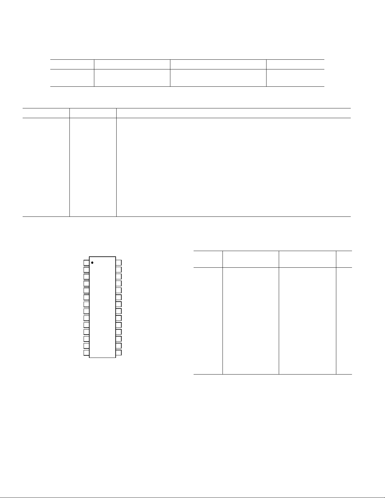
PIN CONFIGURATION
GND
V
VREF OUT
VREF IN
NC
NC
GND
V
AIN
AIN
V
GND
ENCODE
OR
1
2
CC
3
4
5
6
AD9071BR
TOP VIEW
7
(Not to Scale)
8
CC
9
10
11
CC
12
13
14
NC = NO CONNECT
28
27
26
25
24
23
22
21
20
19
18
17
16
15
D0
D1
D2
D3
D4
GND
V
DD
GND
V
DD
D5
D6
D7
D8
D9 (MSB)
Table I. Output Coding
Offset
Code AIN–AIN Binary OR
1023 ≥ 0.512 V 11 1111 1111 1
1023 0.511 V 11 1111 1111 0
1022 0.510 V 11 1111 1110 0
•• ••
•• ••
•• ••
513 0.001 V 10 0000 0001 0
512 0.000 V 10 0000 0000 0
511 –0.001 V 01 1111 1111 0
•• ••
•• ••
•• ••
1 –0.511 V 00 0000 0001 0
0 –0.512 V 00 0000 0000 0
0 ≤–0.513 V 00 0000 0000 1
–4–
REV. C
Page 5

AD9071
SAMPLE N–1
AIN
ENCODE
D9–D0
SAMPLE N SAMPLE N+3 SAMPLE N+4
t
A
t
t
EH
EL
DATA N–4 DATA N–3 DATA N–2 DATA N–1 DATA N DATA N+1
Figure 1. Timing Diagram
V
CC
AIN
AIN
Figure 2. Equivalent Analog Input Circuit
1/f
SAMPLE N+2SAMPLE N+1
s
t
PD
t
V
V
DD
D
, OR
9–0
Figure 5. Equivalent Digital Output Circuit
V
CC
VREF IN
Figure 3. Equivalent Reference Input Circuit
V
CC
ENCODE
Figure 4. Equivalent Encode Input Circuit
V
CC
VREF
OUT
Figure 6. Equivalent Reference Output Circuit
–5–REV. C
Page 6

AD9071
–Typical Performance Characteristics
0
FUNDAMENTAL = –1.0dBFS
SNR = 56.75dB
SINAD = 56.56dB
2ND HARMONIC = –71.88dB
3RD HARMONIC = –77.28dB
MHz
50
dB
–100
–10
–20
–30
–40
–50
–60
–70
–80
–90
0
TPC 1. Spectrum: FS = 100 MSPS, fIN = 10.3 MHz
0
FUNDAMENTAL = –1.0dBFS
–10
SNR = 55.23dB
SINAD = 54.35dB
–20
2ND HARMONIC = –68.28dB
3RD HARMONIC = –62.83dB
–30
–40
–50
dB
–60
–70
–80
–90
–100
0
MHz
50
0
F1 = 41.1MHz
–10
F2 = 42.1MHz
F1 = F2 = –7.0dBFS
–20
–30
–40
–50
dB
–60
–70
–80
–90
–100
0
MHz
TPC 4. Two-Tone Intermodulation Distortion
60
58
56
dB
54
52
50
48
46
44
42
40
10
20
40 60 80
SNR
fIN – MHz
SINAD
100
120 140
50
TPC 2. Spectrum: FS = 100 MSPS, fIN = 41 MHz
0
F1 = 9.63MHz
F2 = 10.63MHz
F1 = F2 = –7.0dBFS
dB
–100
–10
–20
–30
–40
–50
–60
–70
–80
–90
0
MHz
TPC 3. Two-Tone Intermodulation Distortion
TPC 5. SINAD/SNR vs. fIN: FS = 100 MSPS
58
57
56
55
54
53
dB
52
51
50
49
48
50
10 120
40 60 80
20 100 140
F
S
– MSPS
SNR
SINAD
TPC 6. SINAD/SNR vs. FS: fIN = 10.3 MHz
–6–
REV. C
Page 7

AD9071
60
SNR
55
50
dB
45
40
–40 85
–15 5 25
SINAD
T
C
55
TPC 7. Differential SNR vs. TC: fIN = 10.3 MHz
60
58
56
54
52
50
dB
48
46
44
42
40
–40 85
–15 5 25
SINAD
SNR
T
C
55
60
58
56
54
52
50
dB
48
46
44
42
40
2.5 7.5
3.5 4.5 5.5
SNR
SINAD
6.5
ENCODE PULSEWIDTH – ns
TPC 9. SNR vs. Clock Pulsewidth (tEH): fIN = 10.3 MHz
0
–1
dB
–2
–3
–4
–5
–6
–7
15
105
60
150 195 240 285 330 375 420
fIN – MHz
–3dB ROLLOFF POINT
TPC 8. Single-Ended SNR vs. TC: fIN = 10.3 MHz
90
80
70
60
50
dBc
40
30
20
10
0
10 20 30
TPC 11. Second Harmonic Performance: SingleEnded vs. Differential Input
fIN – MHz
TPC 10. Frequency Response
DIFFERENTIAL INPUT
SINGLE-ENDED
40
–7–REV. C
Page 8

AD9071
APPLICATION NOTES
THEORY OF OPERATION
The AD9071 employs a two-step subranging architecture with
digital error correction.
The sampling and conversion process is initiated by a rising edge
at the ENCODE input. The analog input signal is buffered by a
high speed differential amplifier and applied to a track-and-hold
(T/H) circuit, which captures the value of the input at the sampling instant and maintains it for the duration of the conversion.
The coarse quantizer (ADC) produces a 5-bit estimate of the
input value. Its digital output is reconverted to analog form by
the reconstruction DAC and subtracted from the input signal in
the SUM AMP. The second stage quantizer generates a 6-bit
representation of the difference signal. The eleven bits are presented to the ENCODE LOGIC, which corrects for range overlap errors and produces an accurate 10-bit result.
Data are strobed to the output on the rising edge of the ENCODE
input, with the data from sample N appearing on the output
following ENCODE rising edge N+3.
USING THE AD9071
ENCODE Input
Any high-speed A/D converter is extremely sensitive to the
quality of the sampling clock provided by the user. A track/hold
circuit is essentially a mixer, and any noise, distortion, or timing
jitter on the clock will be combined with the desired signal at
the A/D output. For that reason, considerable care has been
taken in the design of the ENCODE input of the AD9071, and
the user is advised to give commensurate thought to the clock
source. The lowest jitter clock source is a crystal oscillator producing a pure sine wave.
The ENCODE input is fully TTL/CMOS compatible.
Digital Outputs
The digital outputs are CMOS compatible for lower power
consumption. 200 Ω series resistors are recommended between
the AD9071 and the receiving logic to reduce transients and
improve SNR.
Analog Input
The analog input has been optimized for differential signal input.
V
(+2.5V)
REF
100⍀ 100⍀
AIN
AD9071
AIN
50⍀
T1A
T1 - 1T
0.1F
0.1F
Figure 7. Differential Analog Input Configuration
If driven single-endedly, the AIN should be connected to a
clean reference and bypassed to ground. For best dynamic
performance, impedances at AIN and AIN should match.
Special care was taken in the design of the analog input section
of the AD9071 to prevent damage and corruption of data when
the input is overdriven. The nominal input range is 1.988 V
to 3.012 V (1.024 V p-p centered at 2.5 V). Out-of-range
comparators detect when the analog input signal is out of this
range, and set the OR output signal HIGH. The digital outputs
are locked at plus or minus full scale (3FF
or 200H) for volt-
H
ages that are out of range, but between 1 V and 5 V. Input voltages outside of this range may result in invalid codes at the
ADC’s output.
V
(+2.5V)
REF
0.1F
100⍀ 100⍀
AIN
AD9071
AIN
0.1F
50⍀
25⍀
Figure 8. Single-Ended Analog Input Configuration
When the analog input signal returns to the nominal range, the
out-of-range comparators return the ADC to its active mode
and the device recovers in the overvoltage recovery time.
Voltage Reference
A stable and accurate 2.5 V voltage reference (VCC – 2.5 V) is
built into the AD9071 (VREF OUT). In normal operation, the
internal reference is used by strapping Pins 3 and 4 of the AD9071
together. The internal reference can provide 100 µA of extra
drive current that may be used for other circuits.
Some applications may require greater accuracy, improved
temperature performance, or adjustment of the gain of the
AD9071, which cannot be obtained by using the internal reference. For these applications, an external 2.5 V reference can be
connected to VREF IN, which requires 5 µA of drive current
(see Figure 9).
+5V
1F
+5V
AD780
+V
IN
GND
O/P SELECT
NC
V
OUT
TRIM
0.1F
1M⍀
25k⍀
NC = NO CONNECT
AD9071
V
IN
REF
Figure 9. Using the AD780 Voltage Reference
The input range can be adjusted by varying the reference voltage
applied to the AD9071. No appreciable degradation in performance occurs when the reference is adjusted ±4%. The fullscale range of the ADC tracks reference voltage changes linearly.
Timing
The performance of the AD9071 is insensitive to the duty
cycle of the clock over a wide range of operating conditions
(see TPC 9).
The AD9071 provides latched data outputs, with three pipeline
delays. Data outputs are available one propagation delay (t
PD
)
after the rising edge of the encode command (see Figure 1). The
length of the output data lines, and loads placed on them, should
be minimized to reduce transients within the AD9071; these
transients can detract from the converter’s dynamic performance.
–8–
REV. C
Page 9

AD9071
The minimum guaranteed conversion rate of the AD9071 is
40 MSPS. At clock rates below 40 MSPS, dynamic performance
may degrade. The AD9070 will operate in bursts, but the user
must flush the internal pipeline each time the clock restarts.
Valid data will be produced on the fourth rising edge of the
ENCODE signal after the clock is restarted.
EVALUATION BOARD
The AD9071 evaluation board is a convenient and easy way to
evaluate the performance of the AD9071 in the SOIC package.
The board consists of an internal voltage reference or an optional
external reference, two 74LCX574 latches for capturing data
from the A/D converter, and an AD9760 DAC for viewing
reconstructed A/D data. The AD9071 output logic can be driven
at 5 V and 3.3 V levels. The latches are set up at 3.3 V but are
5 V tolerant. Test points are provided at Encode, DB9, DB0,
Data Ready, and Data Clock. All are clearly labeled.
Analog Input
The evaluation board can be driven single-ended or differentially. Differential input requires using a 1:1 transformer. For
single-ended operation (J2), Jumper S5 is connected to S8 and
S6 is connected to S7. For differential input operation (J3), S5
is connected to S3 and S4 is connected to S6. The board is
shipped in the differential configuration.
Encode
The AD9071 encode inputs are driven single-ended into J1 and
are at TTL logic levels.
Data Out
The data delivered out of the AD9071 is in offset binary format
at TTL levels. The Data Ready signal can be inverted by opening the S1 and S2 connections. An optional series termination
resistor on Data Ready (R33), normally 0 ohms, is provided to
support various user output impedance configurations. The
AD9760 DAC supports viewing reconstructed A/D data at J4.
Voltage Reference
The AD9071 can be operated using its internal voltage reference
(connect E2 to E3) or an optional external reference (connect
E1 to E2). The board is shipped utilizing the internal voltage
reference.
Layout
The AD9071 is not layout sensitive if some important guidelines
are met. The evaluation board layout provides an example where
these guidelines have been followed to optimize performance.
•
Provide a good ground plane connecting the analog and
digital sections.
•
Excellent bypassing is essential. Chip capacitors with 0.1 µF
values and 0803 dimensions are placed flush against the pins.
Placing any of the capacitors on the bottom of the board can
degrade performance. These techniques reduce the amount
of parasitic inductance that can impact the bypassing ability
of the caps.
•
Separate power planes and supplies for the analog and digital
sections are recommended.
The AD9071 evaluation board is provided as a design example
for customers of Analog Devices. ADI makes no warranties
express, statutory, or implied regarding merchantability or fitness for a particular purpose.
Figure 10. Printed Circuit Board Top Side Silkscreen
Figure 11. Printed Circuit Board Bottom Side Silkscreen
–9–REV. C
Page 10

AD9071
Figure 12. Printed Circuit Board Top Side Copper
Figure 13. Printed Circuit Board Ground Layer
Figure 14. Printed Circuit Board “Split” Power Layer
Figure 15. Printed Circuit Board Bottom Side Copper
–10–
REV. C
Page 11

–11–REV. C
VREF EXT
C7
R5
50⍀
4
6
T1 – 1T
R6
50⍀
S1
S2
4.99k⍀
+VD
VREF EXT
C17
0.1F
T1
R31
0.1F
3
2
1
C5
0.1F
C4
0.1F
12
13
10
C1
0.1F
C8
0.1F
SMB
A IN
J2
2, 3, 4,
5 - GND
SMB
A IN DIF
J3
2, 3, 4,
5 - GND
R4
50⍀
Figure 16. Printed Circuit Board Schematic
SMB
ENCODE IN
J1
2, 3, 4,
5 - GND
TB1
1
GND
2
V
CC
3
4
V
DD
5
+VD
6
C20
TB6
10F
C19
10F
1
2
9
4
5
S9
S4
U5
74LCX86
+ VD : 14
GND : 7
C17
0.1F
C21
10F
C15
0.1F
S8
S5S3
S10
S6
S7
E1
1
100⍀
GND
C22
0.1F
3
11
8
6
E3
R1
C3
0.1F
VREF INT
1
E2
VREF
1
ANALOG IN
R19
100⍀
ANALOG IN
R32
25⍀
ENCODE
DATA CLK
DATA READY
TP4
C6
0.1F
C11
0.1F
C18
10F
C12
0.1F
C2
0.1F
V
CC
C13
0.1F
3
VREF OUT
4
VREF IN
5
DNC
6
DNC
9
AIN
10
AIN
13
ENCODE
V
: 2, 8, 11
CC
TP1
V
DD
GND : 1, 7 12, 21, 23
TP5
V
CC
V
DD
+VD
+VD
R9
24
28
27
26
25
24
19
18
17
16
15
14
DB2
COMP2
200⍀
200⍀
DB3
23
C9
0.1F
R3
R10
200⍀
R11
200⍀
R18
200⍀
DB4
COMP1
R12
200⍀
200⍀
200⍀
200⍀
200⍀
R17
200⍀
TP2
DB5
AD9760
19
R13
R14
R15
R16
FSADJ
DB6
18
R2
2k⍀
TP3
D0
D1
D2
D3
D4
U3
AD9071
: 20, 22
28
D5
D6
D7
D8
D9
OR
10987654321
DB0
DB1
CLK
DVDD
AVDD
27
C14
0.1F
DB7
17
DB8
REFLOREFIO
1
2
3
4
5
6
7
8
9
1
2
3
4
5
6
7
8
9
C10
0.1F
U1
74LCX574
OUT EN
D0
D1
D2
D3
D4
D5
D6
D7
CLOCK
GND : 10
+VD : 20
U2
74LCX574
OUT EN
D0
D1
D2
D3
D4
D5
D6
D7
CLOCK
GND : 10
+VD : 20
+VD
DB9
SLEEP
16
Q0
Q1
Q2
Q3
Q4
Q5
Q6
Q7
Q0
Q1
Q2
Q3
Q4
Q5
Q6
Q7
150⍀
DB0
DB1
DB2
DB3
DB4
DB5
DB6
DB7
DB8
DB9
IOUTA
15
19
18
17
16
15
14
13
12
11
19
18
17
16
15
14
13
12
11
R34
IOUTB
S13
S12
22
21
DB0
DB1
DB2
DB3
DB4
DB5
DB6
DB7
DB8
DB9
OR
R35
150⍀
S11
DB0
DB1
DB2
DB3
DB4
DB5
DB6
DB7
DB8
DB9
OR
DAC OUT
R7
50⍀
+VD
R27
100⍀
R26
100⍀
R25
100⍀
R24
100⍀
R23
100⍀
R22
100⍀
R21
100⍀
R20
100⍀
R29
100⍀
R28
100⍀
R30
100⍀
DATA READY
SNS
J4
2, 3, 4,
5, - GND
R8
50⍀
DATABIT 0
DATABIT 1
DATABIT 2
DATABIT 3
DATABIT 4
DATABIT 5
DATABIT 6
DATABIT 7
DATABIT 8
DATABIT 9
OVERRANGE
R33
0⍀
+VD
J5
1
2
3
4
5
6
7
8
9
10
11
12
13
14
15
16
17
18
19
20
R36
150⍀
GND
GND
R37
150⍀
GND
DATA READY
DATABIT 0
DATABIT 1
DATABIT 2
DATABIT 3
DATABIT 4
DATABIT 5
DATABIT 6
DATABIT 7
DATABIT 8
DATABIT 9
OVERRANGE
C37DPPF
1
2
3
4
5
6
7
8
9
10
11
12
13
14
15
16
17
18
P2
19
20
21
22
23
24
25
26
27
28
29
30
31
32
33
34
35
36
37
AD9071
Page 12

AD9071
Table II. Printed Circuit Board Bill of Materials
Item # Quantity Reference Description
1 18 C1, C2, C3, C4, C5, C6, C7, C8, C9, C10, Ceramic Chip Capacitor, 0603, 0.1 µF
C11, C12, C13, C14, C15, C16, C17, C22
2 4 C18, C19, C20, C21 Tantalum Chip Capacitor, 10 µF
3 3 E1, E2, E3 Jumpers
4 4 J1, J2, J3, J4 SMB-P Connector
5 1 J5 20-Pin Male Header
6 1 P2 37-Pin Connector (Amp 747462-4)
7 13 R1, R19, R20, R21, R22, R23, R24, R25, Surface Mount Resistor, 1206, 100 Ω
R26, R27, R28, R29, R30
8 1 R2 Surface Mount Resistor, 1206, 2000 Ω
9 11 R3, R9, R10, R11, R12, R13, R14, R15, Surface Mount Resistor, 1206, 200 Ω
R16, R17, R18
10 5 R4, R5, R6, R7, R8 Surface Mount Resistor, 1206, 50 Ω
11 1 R31 Surface Mount Resistor, 1206, 5000 Ω
12 1 R32 Surface Mount Resistor, 1206, 25 Ω
13 1 R33 Surface Mount Resistor, 1206, 0 Ω
14 4 R34, R35, R36, R37 Surface Mount Resistor, 1206, 150 Ω
15 13 S1, S2, S3, S4, S5, S6, S7, S8, S9, S10, Jumpers
S11, S12, S13
16 1 T1 Surface Mount Transformer Mini-Circuit T1-T1, 1:1 Ratio
17 1 TB1 6-Pin Wieland Connector (P/N # 25,602, 2653.0; 25.530
3625.0)
18 5 TP1, TP2, TP3, TP4, TP5 Test Points
19 2 U1, U2 74LCX574 Octal Latch
20 1 U3 AD9071BR, 10-Bit, 100 MSPS, ADC
21 1 U4 AD9760AR, 10-Bit, 125 MSPS, DAC
22 1 U5 74LCX86, XOR
C00567b–0–8/01(C)
OUTLINE DIMENSIONS
Dimensions shown in inches and (mm).
28-Lead Wide Body SOIC
(R-28)
0.7125 (18.10)
0.6969 (17.70)
0.2992 (7.60)
0.2914 (7.40)
0.0118 (0.30)
0.0040 (0.10)
28
1
PIN 1
0.0500
(1.27)
BSC
0.0192 (0.49)
0.0138 (0.35)
15
14
0.1043 (2.65)
0.0926 (2.35)
SEATING
PLANE
0.4193 (10.65)
0.3937 (10.00)
0.0125 (0.32)
0.0091 (0.23)
0.0291 (0.74)
0.0098 (0.25)
8°
0°
ⴛ 45ⴗ
0.0500 (1.27)
0.0157 (0.40)
AD9071–Revision History
Location Page
Data Sheet changed from REV. B to REV. C.
Edits to ABSOLUTE MAXIMUM RATINGS . . . . . . . . . . . . . . . . . . . . . . . . . . . . . . . . . . . . . . . . . . . . . . . . . . . . . . . . . . . . . . . . . 3
PRINTED IN U.S.A.
–12–
REV. C
 Loading...