

Page 1
10-Bit, 100 MSPS
T/H
DAC
ADC
VREF
IN
–2.5V
VREF
OUT COMP
REF
BYPASS
SOIC (BR)
PACKAGE
ONLY
ADC
SUM
AMP
TIMING
AIN
ENCODE
ENCODE
AIN
AD9070
ENCODE
LOGIC
D9 – D0
DIP
PACKAGE
ONLY
OR
10
V
EE
GND
a
FEATURES
10-Bit, 100 MSPS ADC
Low Power: 600 mW Typical at 100 MSPS
On-Chip Track/Hold
230 MHz Analog Bandwidth
SINAD = 54 dB @ 41 MHz
On–Chip Reference
1 V p-p Analog Input Range
Single Supply Operation: +5 V or –5 V
Differential Clock Input
Available in Standard Military Drawing Version
APPLICATIONS
Digital Communications
Signal Intelligence
Digital Oscilloscopes
Spectrum Analyzers
Medical Imaging
Radar
HDTV
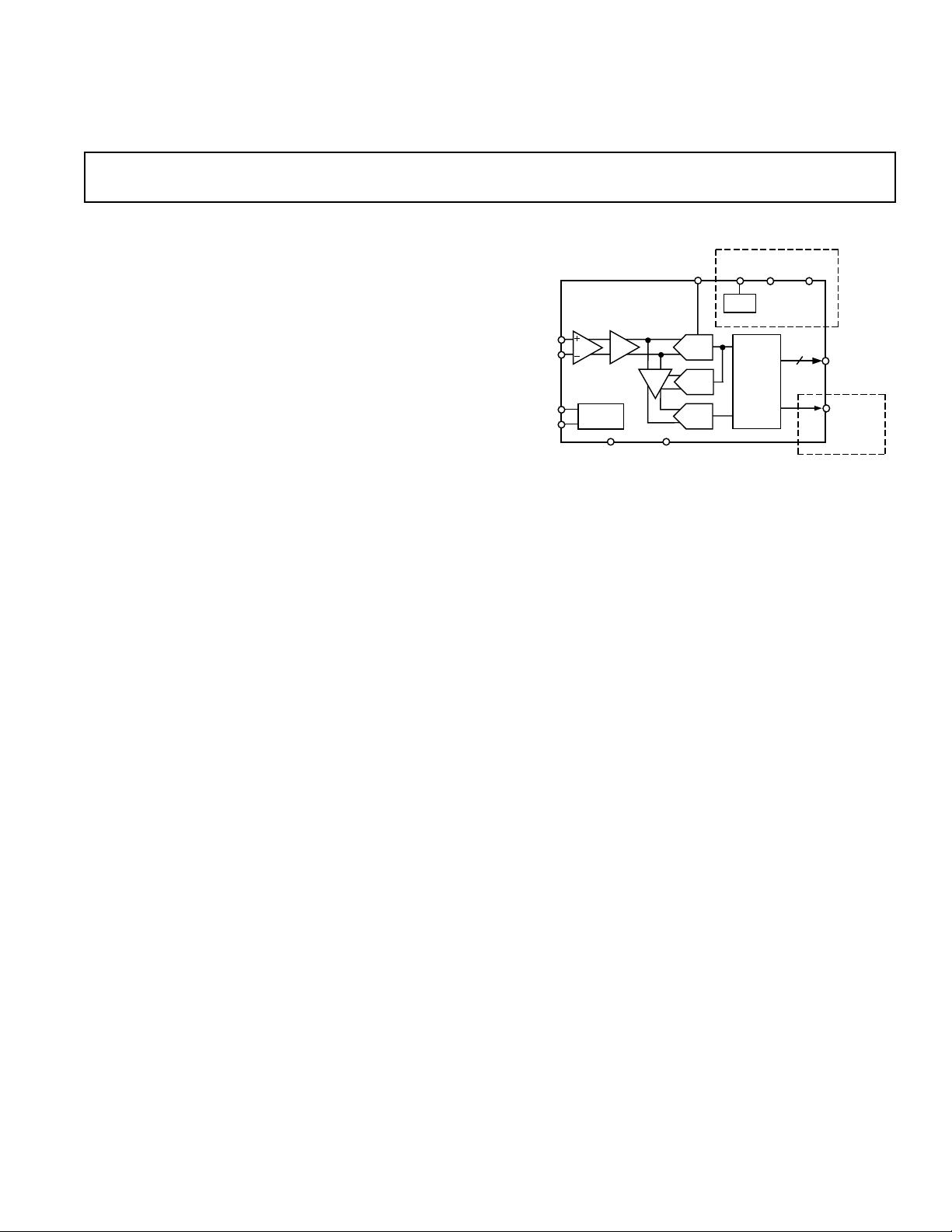
GENERAL DESCRIPTION
The AD9070 is a monolithic sampling analog-to-digital
converter with an on-chip track-and-hold circuit and ECL
digital interfaces. The product operates at a 100 MSPS
conversion rate with outstanding dynamic performance over
its full operating range.
The ADC requires only a single –5 V supply and an encode
clock for full performance operation. The digital outputs are
ECL compatible, while a differential clock input accommodates
a wide range of logic levels. The AD9070 may be operated in a
Positive ECL (PECL) environment with a single +5 V supply.
An Out-of-Range output (OR) is available in the DIP version to
indicate that a conversion result is outside the operating range.
In both package styles, the output data are held at saturation
levels during an out-of-range condition.
A/D Converter
AD9070
FUNCTIONAL BLOCK DIAGRAM
The input amplifier supports single-ended interfaces. An
internal –2.5 V reference is included in the SOIC packaged
device (an external voltage reference is required for the DIP
version).
Fabricated on an advanced bipolar process, the AD9070
is available in a plastic SOIC package specified over the
industrial temperature range (–40°C to +85°C), and a full
MIL-PRF-38534 QML version (–55°C to +125°C) in a
ceramic Dual-in-Line Package (DIP).
REV. B
Information furnished by Analog Devices is believed to be accurate and
reliable. However, no responsibility is assumed by Analog Devices for its
use, nor for any infringements of patents or other rights of third parties
which may result from its use. No license is granted by implication or
otherwise under any patent or patent rights of Analog Devices.
One Technology Way, P.O. Box 9106, Norwood, MA 02062-9106, U.S.A.
Tel: 781/329-4700 World Wide Web Site: http://www.analog.com
Fax: 781/326-8703 © Analog Devices, Inc., 2000
Page 2

(VEE = –5 V, ENCODE = 100 MSPS, outputs loaded with 100 ⍀ to –2 V unless
AD9070–SPECIFICATIONS
Parameter Temp Level Min Typ Max Min Typ Max Units
RESOLUTION 10 10 Bit
DC ACCURACY
Differential Nonlinearity +25°CI ± 0.6 +1.25/–1.0 ± 0.6 +1.25/–1.0 LSB
Integral Nonlinearity +25°CI ± 0.6 ± 1.5 ± 0.6 ± 1.5 LSB
No Missing Codes Full VI Guaranteed Guaranteed
Gain Error
Gain Tempco
ANALOG INPUT
Input Voltage Range (with Respect to AIN) Full V ± 512 ± 512 mV p-p
Common-Mode Voltage Full V –2.5 ± 0.2 –2.5 ± 0.2 V
Input Offset Voltage +25°CI ± 7 ± 18 ± 7 ± 18 mV
Input Resistance +25°C I 10 40 10 40 kΩ
Input Capacitance +25°CV 3 3 pF
Input Bias Current +25°C I 75 200 75 200 µA
Analog Bandwidth, Full Power +25°C V 230 230 MHz
1
1
otherwise noted)
Test AD9070BR 5962-9756301HXC
Full VI ± 0.7 +1.5/–1.0 ± 0.9 +2.00/–1.0 LSB
Full VI ± 0.9 ± 1.5 ± 2.25 LSB
+25°CI ± 1 ± 4 ± 1 ± 4% FS
Full VI ± 2 ± 6% FS
Full V 115 130 ppm/°C
Full I ± 8 ± 9 ± 20 mV
Full I 40 10 40 kΩ
Full I 75 75 200 µA
REFERENCE OUTPUT
Output Voltage Full VI –2.4 –2.5 –2.6 N/A V
Temperature Coefficient Full V 170 N/A ppm/°C
SWITCHING PERFORMANCE
Maximum Conversion Rate Full VI 100 100 MSPS
Minimum Conversion Rate Full IV 40 40 MSPS
Encode Pulse Width High (tEH) +25°CIV 4.5 13 4.5 13 ns
Encode Pulse Width Low (t
Aperture Delay (t
) +25°C V 0.85 0.85 ns
A
Aperture Uncertainty (Jitter) +25°C V 2.5 2.5 ps rms
Output Valid Time (tV)
Output Propagation Delay (t
Output Rise Time (t
) Full VI 0.5 0.5 1.2 ns
R
) +25°CIV 4.5 13 4.5 13 ns
EL
2
2
)
PD
Full VI 1.5 2.6 1.5 2.6 ns
Full VI 3.0 4.0 3.0 4.0 ns
Output Fall Time (tF) Full VI 0.5 0.5 1.2 ns
DIGITAL INPUTS
Logic “1” Voltage Full IV –1.1 –0.4 –1.1 –0.4 V
Logic “0” Voltage Full IV –1.5 –1.5 V
Logic “1” Current Full VI ±10 ± 10 µA
Logic “0” Current Full VI ±10 ± 10 µA
Input Capacitance +25°CV 3 3 pF
DIGITAL OUTPUTS
Logic “1” Voltage Full VI –1.1 –1.15 V
Logic “0” Voltage Full VI –1.65 –1.60 V
Output Coding Twos Complement Twos Complement
POWER SUPPLY
VEE Supply Current (VEE = –5 V) Full VI 80 120 150 80 120 150 mA
Power Dissipation
Power Supply Sensitivity
3
4
Full VI 400 600 750 400 600 750 mW
+25°C I 0.005 0.012 0.005 0.012 V/V
–2–
REV. B
Page 3
AD9070
Test AD9070BR 5962-9756301HXC
Parameter Temp Level Min Typ Max Min Typ Max Units
DYNAMIC PERFORMANCE
Transient Response +25°CV 3 3 ns
Overvoltage Recovery Time +25°CV 4 4 ns
Signal-to-Noise Ratio (SNR)
(Without Harmonics)
= 10.3 MHz +25°C I 55 57 55 57 dB
f
IN
fIN = 41 MHz +25°C I 54 56 54 56 dB
Signal-to-Noise Ratio (SINAD)
(With Harmonics)
= 10.3 MHz +25°C I 54 56 54 56 dB
f
IN
fIN = 41 MHz +25°C I 51 54 51 54 dB
Effective Number of Bit
= 10.3 MHz +25°C I 8.8 9.2 8.8 9.2 Bits
f
IN
= 41 MHz +25°C I 8.3 8.9 8.3 8.9 Bits
f
IN
2nd Harmonic Distortion
fIN = 10.3 MHz +25°C I 63 70 63 70 dBc
= 41 MHz +25°C I 58 63 58 63 dBc
f
IN
3rd Harmonic Distortion
fIN = 10.3 MHz +25°C I 65 71 65 71 dBc
= 41 MHz +25°C I 57 61 57 61 dBc
f
IN
Two-Tone Intermod Distortion (IMD)
fIN = 10.3 MHz +25°C V 70 70 dBc
fIN = 41 MHz +25°C V 60 60 dBc
NOTES
1
Gain error and gain temperature coefficient are based on the ADC only (with a fixed –2.5 V external reference).
2
tV and tPD are measured from the threshold crossing of the ENCODE input to the 50% levels of the digital outputs. The output ac load during test is 10 pF.
3
Power dissipation is measured under the following conditions: fS 100 MSPS, analog input is –1 dBfs at 10.3 MHz. Power dissipation does not include the current of
the external ECL pull-down resistors that set the current in the ECL output followers.
4
A change in input offset voltage with respect to a change in VEE.
5
SNR/harmonics based on an analog input voltage of –1.0 dBfs referenced to a 1.024 V full-scale input range.
Typical thermal impedance for the R style (SOIC) 28-lead package: θJC = 23°C/W, θCA = 48°C/W, θJA = 71°C/W.
Typical thermal impedance for the DH style (Ceramic DIP) 28-lead package: θJC = 8°C/W, θCA = 43°C/W, θJA = 51°C/W.
Contact DSCC to obtain the latest revision of the 5962-9756301 drawing.
Specifications subject to change without notice.
5
Full V 56 55 dB
Full V 55 54 dB
Full V 55 54 dB
Full V 53 52 dB
REV. B
AIN
D9–D0
ENCODE
ENCODE
SAMPLE N–1
SAMPLE N SAMPLE N+3 SAMPLE N+4
1/fs
SAMPLE N+2SAMPLE N+1
t
PD
t
V
t
A
t
t
EH
EL
DATA N–4 DATA N–3 DATA N–2 DATA N–1 DATA N DATA N+1
Figure 1. Timing Diagram
–3–
Page 4
AD9070
WARNING!
ESD SENSITIVE DEVICE
ABSOLUTE MAXIMUM RATINGS*
VEE . . . . . . . . . . . . . . . . . . . . . . . . . . . . . . . . . . . . . . . . . –6 V
Analog Inputs . . . . . . . . . . . . . . . . . . . . . V
Digital Inputs . . . . . . . . . . . . . . . . . . . . . . . . . . . V
VREF IN, VREF OUT . . . . . . . . . . . . . . . . . . . . V
–1 V to +1.0 V
EE
to 0.0 V
EE
to 0.0 V
EE
Digital Output Current . . . . . . . . . . . . . . . . . . . . . . . . 20 mA
Operating Temperature . . . . . . . . . . . . . . . . –55°C to +125°C
Storage Temperature . . . . . . . . . . . . . . . . . . –65°C to +150°C
Maximum Junction Temperature . . . . . . . . . . . . . . . +175°C
Maximum Case Temperature . . . . . . . . . . . . . . . . . . +150°C
*Stresses above those listed under Absolute Maximum Ratings may cause perma-
nent damage to the device. This is a stress rating only; functional operation of the
device at these or any other conditions outside of those indicated in the operation
sections of this specification is not implied. Exposure to absolute maximum ratings
for extended periods may affect device reliability.
EXPLANATION OF TEST LEVELS
Test Level
I – 100% production tested.
II – 100% production tested at +25°C and sample tested at
specified temperatures.
III – Sample tested only.
IV – Parameter is guaranteed by design and characterization
testing.
V – Parameter is a typical value only.
VI – 100% production tested at +25°C; guaranteed by design
and characterization testing for industrial temperature
range; 100% production tested at temperature extremes
for military devices.
Table I. Output Coding
Twos
Step AIN–AIN Code Complement OR
1024 ≥ 0.512 V >511 01 1111 1111 1
1023 0.511 V 511 01 1111 1111 0
1022 0.510 V 510 01 1111 1110 0
•• • • •
•• • • •
•• • • •
513 0.001 V 1 00 0000 0001 0
512 0.000 V 0 00 0000 0000 0
511 –0.001 V –1 11 1111 1111 0
•• • • •
•• • • •
•• • • •
1 –0.511 V –511 10 0000 0001 0
0 –0.512 V –512 10 0000 0000 0
–1 ≤ –0.513 V <512 10 0000 0000 1
ORDERING GUIDE
Model Temperature Range Package Option*
AD9070BR –40°C to +85°C R-28
AD9070/PCB +25°C Evaluation Board
5962-9756301HXC –55°C to +125°C DH-28
*DH = Ceramic DIP; R = Small Outline IC (SOIC).
CAUTION
ESD (electrostatic discharge) sensitive device. Electrostatic charges as high as 4000 V readily
accumulate on the human body and test equipment and can discharge without detection.
Although the AD9070 features proprietary ESD protection circuitry, permanent damage may
occur on devices subjected to high energy electrostatic discharges. Therefore, proper ESD
precautions are recommended to avoid performance degradation or loss of functionality.
–4–
REV. B
Page 5
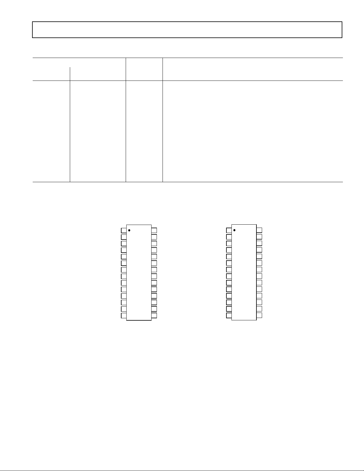
PIN FUNCTION DESCRIPTIONS
Pin Numbers
AD9070BR AD9070DIP
R Package D Package Name Function
AD9070
1, 7, 12, 21, 23 1, 7, 9, 14, 21 V
EE
Negative Power Supply. Nominally –5.0 V.
2, 8, 11, 20, 22 2, 6, 8, 10, 13, 15, 22 GND Ground.
3 N/A VREF OUT Internal Reference Output (–2.5 V typical); Bypass with 0.1 µF to Ground.
4 3 VREF IN Reference Input for ADC (–2.5 V typical).
5 N/A COMP Internal Amplifier Compensation, 0.1 µF to V
6 N/A REF BYPASS Reference Bypass Node, 0.1 µF to V
EE
.
EE
.
94 AIN Analog Input – Complement.
10 5 AIN Analog Input – True.
13 11 ENCODE Encode Clock for ADC (ADC Samples on Rising Edge of ENCODE).
14 12 ENCODE Encode Clock Complement (ADC Samples on Falling Edge of ENCODE).
28–24, 19–15 27–23, 20–16 D9–D0 Digital Outputs of ADC. D9 is the MSB. Data is twos complement.
N/A 28 OR Out-of-Range Output. Goes HIGH when the converted sample is more
positive than 1FFh or more negative than 200h (Twos Complement Coding).
PIN CONFIGURATIONS
SOIC Ceramic DIP
28
27
26
25
24
23
22
21
20
19
18
17
16
15
OR
D9 (MSB)
D8
D7
D6
D5
GND
V
EE
D4
D3
D2
D1
D0 (LSB)
GND
V
GND
VREF OUT
VREF IN
COMP
REF BYPASS
V
GND
AIN
AIN
GND
V
ENCODE
ENCODE
EE
EE
EE
1
2
3
4
5
6
AD9070BR
7
TOP VIEW
(Not to Scale)
8
9
10
11
12
13
14
28
27
26
25
24
23
22
21
20
19
18
17
16
15
D9 (MSB)
D8
D7
D6
D5
V
EE
GND
V
EE
GND
D4
D3
D2
D1
D0 (LSB)
V
GND
VREF IN
AIN
AIN
GND
V
GND
V
GND
ENCODE
ENCODE
GND
V
EE
EE
EE
EE
1
2
3
4
5
6
AD9070DIP
7
TOP VIEW
(Not to Scale)
8
9
10
11
12
13
14
REV. B
–5–
Page 6

AD9070–Typical Circuit Applications
D9 – D0
OR
V
EE
AIN AIN
V
EE
Figure 2. Equivalent Analog Input Circuit
VREF IN
V
EE
Figure 3. Equivalent Reference Input Circuit
ENCODE
ENCODE
V
EE
Figure 4. Equivalent Encode Input Circuit
Figure 5. Equivalent Digital Output Circuit
VREF
OUT
V
EE
Figure 6. Equivalent Reference Output Circuit
–6–
REV. B
Page 7

Typical Performance Characteristics–AD9070
0
–10
–20
–30
–40
–50
dB
–60
–70
–80
–90
–100
0505 1015202530354045
FUNDAMENTAL = –1.0dBfs
SNR = 58.5dB
SINAD = 58.0dB
2nd HARMONIC = –76.8dB
3rd HARMONIC = –68.1dB
MHz
Figure 7. Spectrum: fS = 100 MSPS, fIN = 10 MHz
0
FUNDAMENTAL = –1.0dBfs
–10
SNR = 56.8dB
SINAD = 55.0dB
–20
2nd HARMONIC = –66.6dB
3rd HARMONIC = –60.8dB
–30
–40
–50
dB
–60
–70
–80
–90
–100
0505 1015202530354045
MHz
Figure 8. Spectrum: fS = 100 MSPS, fIN = 40 MHz
0
–10
–20
–30
–40
–50
dB
–60
–70
–80
–90
–100
F1 = 40.1MHz
F2 = 41.0MHz
F1 = F2 = –7.0dBfs
0505 1015202530354045
MHz
Figure 10. Two Tone Intermodulation Distortion
60
55
50
45
40
dB
35
30
25
20
0 16020
SINAD
NYQUIST
FREQUENCY
(50 MHz)
40 60 80 100 120 140
FIN – MHz
SNR
Figure 11. SNR vs. fIN; fS = 100 MSPS
0
–10
–20
–30
–40
–50
dB
–60
–70
–80
–90
–100
0505 1015202530354045
F1 = 9.57MHz
F2 = 10.3MHz
F1 = F2 = –7.0dBfs
MHz
Figure 9. Two Tone Intermodulation Distortion
REV. B
–7–
60
58
56
54
52
50
dB
48
46
44
42
40
0 16020 40 60 80 100 120 140
FS – MSPS
SINAD
Figure 12. SNR vs. fS: fIN = 10.3 MHz
SNR
Page 8

AD9070
60
59
58
57
56
55
dB
54
53
52
51
50
–60 140–40
SNR
SINAD
FS = 100MSPS
= 10.1MHz
F
IN
–200 20406080
TC – ⴗC
100 120
Figure 13. SNR vs. TC: BR Package (SOIC)
60
59
58
57
56
55
dB
54
53
52
51
50
–60 140–40
SNR
SINAD
FS = 100MSPS
= 10.1MHz
F
IN
–200 20406080
T
– ⴗC
100 120
60
59
58
57
56
55
dB
54
53
52
51
50
0101
FS = 100MSPS
= 10.1MHz
F
IN
234567
ENCODE PULSEWIDTH – ns
89
Figure 15. SNR vs. Clock Pulse Width (tEH)
0
–1
–2
NYQUIST
dB
FREQUENCY
–3
–4
–5
50MHz
0 30050
100 150 200 250
FIN – MHz
Figure 14. SNR vs. TC: DIP Package
Figure 16. Frequency Response
–8–
REV. B
Page 9

AD9070
5
APPLICATION NOTES
Theory of Operation
The AD9070 employs a two-step subranging architecture with
digital error correction.
The sampling and conversion process is initiated by a rising
edge at the ENCODE input. The analog input signal is
buffered by a high speed differential amplifier and applied to a
track-and-hold (T/H) circuit that captures the value of the
input at the sampling instant and maintains it for the duration
of the conversion.
The coarse quantizer (ADC) produces a five-bit estimate of the
input value. Its digital output is reconverted to analog form by
the reconstruction DAC and subtracted from the input signal in
the SUM AMP. The second stage quantizer generates a six-bit
representation of the difference signal. The eleven bits are
presented to the ENCODE LOGIC, which corrects for range
overlap errors and produces an accurate ten-bit result.
Data are strobed to the output on the rising edge of the ENCODE
input, with the data from sample N appearing on the output
following ENCODE rising edge N+3.
USING THE AD9070
ENCODE Input
Any high speed A/D converter is extremely sensitive to the quality
of the sampling clock provided by the user. A Track/Hold circuit is
essentially a mixer, and any noise, distortion or timing jitter on
the clock will be combined with the desired signal at the A/D
output. For that reason, considerable care has been taken in the
design of the ENCODE input of the AD9070 and the user is
advised to give commensurate thought to the clock source.
The ENCODE input is fully differential and may be operated in
a differential or a single-ended mode. It has a common-mode
range of –1 V to –3 V, and is easily driven by a differential ECL
driver. Proper termination at the A/D is important.
–5V
V
GND
EE
CLK
(1Vp-p)
0.1F
IN
10k⍀
R
T
1k⍀
0.1F
3k⍀
V
–
AD9070
ENCODE
ENCODE
Figure 17. Single-Ended ENCODE: AC Coupled
In single-ended mode, the ENCODE input must be tied to an
appropriate reference voltage, generally midway between the
high and the low levels of the incoming logic signal. Many ECL
circuits provide a V
reference voltage intended for this
BB
purpose. If a reference voltage is produced by dividing the
power supply voltage, any noise on the supply used will couple
to the clock input and then to the output data. This is not
recommended. A better approach is to develop the required
voltage from the internal or external converter voltage reference
(VREF OUT).
Very small timing errors can reduce the performance of an A/D
dramatically. Total jitter of only 3.2 ps will limit the performance of an A/D sampling a full-scale 50 MHz signal to nine
effective bits. The AD9070’s specified aperture jitter of 2.5 ps
leaves only 2.0 ps of jitter budget for the clock source (an RSS
calculation).
The cleanest clock source is only a crystal oscillator producing a
pure sine wave. In this configuration, or with any roughly
symmetrical clock input, the input can be ac coupled and biased
to a reference voltage that also provides the ENCODE input
(Figure 17). This ensures that the reference voltage is centered
on the ENCODE signal.
Digital Outputs
The digital outputs are compatible with 10K ECL logic. The
suggested pull-down is 100 Ω to –2 V. However, to reduce
power consumption, higher value pull-down resistors can be
used when driving very low capacitance loads or at reduced
encode rates. The falling edge slew rate of the output bits will be
degraded with higher value pull-down resistors.
Analog Input
The analog input to the AD9070 is a differential amplifier, but
the design has been optimized for a single-ended input. The
AIN input should be connected or bypassed to the ground
reference of the input signal. For best dynamic performance,
impedances at AIN and AIN should match.
The circuit in Figure 18 illustrates a simple ac-coupled interface. The midscale input voltage and the AIN levels are both
provided by the internal reference (VREF OUT).
V
1Vp-p
ENCODE
ENCODE
0.1F
IN
500⍀
R
T
0.1F
500⍀
AIN
AIN
VREF OUT
VREF IN
ENCODE
ENCODE
COMP
0.1F
GND
AD9070
(MSB) D9
(LSB) D0
V
EE
–5V
REF
BYPASS
–5V
–5V
0.1F
D9
510⍀
(OR 100⍀ TO –2V)
D0
510⍀
(OR 100⍀ TO –2V)
Figure 18. AD9070 in –5 V (ECL) Environment
REV. B
–9–
Page 10

AD9070
Figure 19 shows typical connections for the analog inputs when
using the AD9070 in a dc-coupled system with single-ended
signals. The AD820 is used to offset the ground referenced
input signal to the level required by the AD9070. A very high
performance amplifier, such as the AD9631, is required to avoid
degrading the analog signal presented to the ADC. A buffered
ac interface is easily implemented, with even fewer components
(Figure 20).
–5V
V
EE
AIN
AD9070
AIN
VREF OUT
VREF IN
GND
V
ⴞ0.5V
350⍀
–5V
+5V
–5V
0.1F
AD9631
1k⍀
0.1F
R
T
0.1F
1k⍀
350⍀
1k⍀
AD820
IN
Figure 19. DC-Coupled Input
–5V
V
EE
AIN
AD9070
AIN
VREF OUT
VREF IN
GND
V
1Vp-p
350⍀
350⍀
IN
R
T
0.1F
+5V
–5V
AD9631
0.1F
500⍀
500⍀
0.1F
0.1F
Figure 20. AC-Coupled Input
Special care was taken in the design of the analog input section
of the AD9070 to prevent damage and corruption of data when
the input is overdriven. The nominal input range is –1.988 V to
–3.012 V (1.024 V p–p centered at –2.5 V). Out-of-range
comparators detect when the analog input signal is out of this
range and set the OR output signal HIGH. The digital outputs
are locked at plus or minus full scale (1FFh or 200h) for
voltages that are out of range but between –1 V and –5 V. Input
voltages outside of this range may result in invalid codes at the
ADCs output.
When the analog input signal returns to the nominal range, the
out-of-range comparators return the ADC to its active mode
and the device recovers in approximately 3 ns.
The input is protected to one volt outside of the power supply
rails. For nominal power (–5 V and ground), the analog input
will not be damaged with signals ranging from –6.0 V to +1.0 V.
Voltage Reference
A stable and accurate –2.5 V voltage reference is built into the
AD9070 (VREF OUT) in the SOIC (BR) package. In normal
operation, the internal reference is used by strapping Pins 3
and 4 of the AD9070 together. The internal reference can
provide 100 µA of extra drive current that may be used for other
circuits.
Some applications may require greater accuracy, improved
temperature performance or adjustment of the gain of the
AD9070, which cannot be obtained by using the internal
reference. For these applications, an external –2.5 V reference
can be connected to VREF IN, which requires 5 µA of drive
current (Figure 21).
–5V
GND
V
EE
VREF OUT
+V
V
IN
OUT
AD780
GND
1.25k⍀
–5V
NC
AD9070
VREF IN
0.1F
Figure 21. Using the AD780 Voltage Reference
The input range can be adjusted by varying the reference
voltage applied to the AD9070. No appreciable degradation in
performance occurs when the reference is adjusted ±4%. The
full-scale range of the ADC tracks reference voltage changes
linearly.
Timing
The performance of the AD9070 is insensitive to the duty cycle
of the clock over a wide range of operating conditions: pulse
width variations of as much as ±20% will cause no degradation
in performance (see Figure 15).
The AD9070 provides latched data outputs, with three pipeline
delays. Data outputs are available one propagation delay (t
PD
)
after the rising edge of the encode command (Figure 1). The
length of the output data lines and loads placed on them should
be minimized to reduce transients within the AD9070; these
transients can detract from the converter’s dynamic performance.
The minimum guaranteed conversion rate of the AD9070 is
40 MSPS. At clock rates below 40 MSPS, dynamic performance
may degrade. The AD9070 will operate in bursts, but the user
must flush the internal pipeline each time the clock restarts.
Valid data will be produced on the fourth rising edge of the
ENCODE signal after the clock is restarted.
–10–
REV. B
Page 11

AD9070
+5 V Operation
The AD9070 may be operated above ground, with a single +5 V
power supply. All power supply ground pins are connected to
+5 V, and V
pins are connected to ground (Figure 22). Care
EE
must be taken in connecting signals and determining bypass rails.
The reference voltage (REF OUT) is still generated with respect
to the positive rail, which is now +5 V. It is nominally +2.5 V,
but its voltage with respect to ground will vary directly with
changes in the power supply voltage (for example, if the power
supply goes to +5.1 V, the reference becomes +2.6 V). The
reference input is likewise processed with respect to +5 V. This
dictates that these pins be bypassed to +5 V as well. However,
the COMP and REF BYPASS pins must continue to be
bypassed to the most negative supply, which is now ground. The
AIN input must still be connected or bypassed to the ground
reference of the input signal.
+5V
0.1F
V
1Vp-p
ENCODE
ENCODE
IN
500⍀
R
T
10H
0.1F
0.1F
+5V
0.1F 0.1F
AIN
AD9070
AIN
VREF OUT
VREF IN
ENCODE
ENCODE
COMP
GND
V
EE
(MSB) D9
(LSB) D0
REF
BYPASS
D9
510⍀
(OR 100⍀ TO +3V)
D0
510⍀
(OR 100⍀ TO +3V)
Package Options
The AD9070 is available in two packages. The BR package is a
standard 28-lead Small Outline IC (SOIC). The DIP package is
a ceramic Dual-in-Line Hybrid. The SOIC is offered in a commercial grade, and specified over the industrial (–40°C to +85°C)
temperature range. The DIP is a full MIL-PRF-38534 QML
version that operates from (–55°C to +125°C).
The SOIC version includes the on-chip voltage reference,
whereas the DIP does not. The DIP, however, provides the
Overrange (OR) output, and includes reference and power
supply bypassing, along with an internal compensation capacitor.
Equivalent performance may be obtained with either part
though, due to the internal bypassing, the DIP is not as sensitive
to board layout and parasitics.
Figure 22. AD9070 in +5 V (PECL) Environment
REV. B
–11–
Page 12

AD9070
AD9070BR EVALUATION BOARD
E1
E2
E3
1k⍀
AIN
50⍀
CLK
J2
50⍀
CLKB
J4
50⍀
E19
1k⍀
–5V
10H176
RECVR
E9E8
ECL
AD780 REFERENCE
VREF OUT
VREF IN
COMP
BYPASS
AIN
AD9070
AIN
ENC
BUFFERED
AND
LATCHED
ON-CARD
ENCODE
ENC
E7 E5
E4 E6
1 OF 2
10H176
HEX D FF
PIN 2
TO CARD
CONNECT
1 OF 4
10H116
CARD
CONNECTOR
PIN 21
Figure 23.
The AD9070 evaluation board is a convenient and easy way to
evaluate the performance of the AD9070 in the SOIC package.
The board consists of an AD780 voltage reference (configured
for –2.5 V), two 10H176 (hex D flip flop) for capturing data
from the A/D converter and five 10H116 triple line receivers for
buffering the encode signal and driving the data via the edge
connector. Termination resistors (RP11, RP12, and RP14) are
provided for the data leaving the board via the connector; (they
can be removed if termination resistors are already provided by
the user).
Analog Input
The evaluation board requires a 1 V peak-to-peak signal
centered at ground (J1). This signal is ac coupled and then dc
shifted –2.5 V before it is input to the A/D converter.
Encode
The AD9070 encode inputs can be driven single ended
(connect E9 to E19 and drive J2 with an ECL signal) or
differentially (connect E8 to E19 and drive J2 and J4 with
differential ECL signals). The board is shipped in single ended
configuration. The differential encode signal leaving the board
via the connector can be inverted by interchanging E4, E5, E6,
and E7 (connect E4 to E7 and E5 to E6 or E4 to E6 and E7 to
E5). This ensures that the user will be able to capture the data
coming from the evaluation board.
Data Out
Data goes single-ended into the 10H116 flip flops but comes
out differentially. The data coming out of the AD9070 is in twos
complement format, but is changed to straight binary by
inverting the MSB at the connector (on the schematic Bit 1 and
Bit 1B are swapped).
Voltage Reference
The AD9070 can be operated using its internal bandgap
reference (connect E2 to E3) or the on board AD780 external
reference (connect E1 to E3). The board is shipped utilizing the
internal voltage reference.
Layout
The AD9070 is not layout sensitive if some important guidelines are met. The evaluation board layout provides an
example where these guidelines have been followed to
optimize performance.
• Provide a good ground plane connecting the analog and
digital sections.
• Excellent bypassing is essential. Chip caps with 0.1 µF values
and 0603 dimensions are placed flush against the pins.
Placing any of the caps on the bottom of the board can
degrade performance. These techniques reduce the amount
of parasitic inductance which can impact the bypassing ability
of the caps.
• Separate power planes and supplies for the analog and digital
sections are recommended.
The AD9070 evaluation board is provided as a design example
for customers of Analog Devices. ADI makes no warranties
express, statutory, or implied regarding merchantability or
fitness for a particular purpose.
–12–
REV. B
Page 13

D2
D1
D2
D1
D0
D0
Q2
Q2
Q1
Q1
Q0
Q0
BIT1
13
10
12
9
5
4
2
3
6
7
14
15
Q2
DR
DRB
Q1
VBB
11
BIT2B
E4
E5
E6
E7
ADRB
ADR
BIT2B
BIT1
C15
0.1F
C37DRPF
CON1
NC
+VIN
TEMP
GND
1
2
3
4
5
6
7
8
OP
NC
VOUT
TRIM
U2
AD780N
R1
1.25k⍀
C2
1F
VREFOUT
VREFIN
COMP
REF
BYPASS
AIN
AIN
ENCODE
ENCODE
V
EE
GND
GND
GND
3
4
5
6
U1
AD9070BR
9
10
–5V
–5V
–5V
GND
GND
GND
GND
GND
(MSB) D9
D8
D7
D5
D4
D3
D2
D1
(LSB) D0
D6
13
14
1
7
12
2
11
8
21
23
28
27
26
25
24
19
18
17
16
15
22
20
E2
E1
E3
–5V
C7
0.1F
C6
0.1F
–5V
R6
1.0k⍀
C3
0.1F
R5
50⍀
R4
1k⍀
GND
C8
0.1F
C4
0.1F
R2
50⍀
BNC
J1
CLK
R10
50⍀
CLKB
E19
9
10
6
7
U11
10H116
ENCENCB
R3
50⍀
E8 E9
U11
10H116
11
C16
0.1F
U11
10H116
CLKB
CLK
DRB
14
1512
13
DR
GND
GND
D0
D2
D1
D3
D4
D5
CLK
Q0
Q1
Q2
Q3
Q4
Q5
Q1
Q2
Q3
Q4
Q5
5
7
6
10
11
12
9
15
14
13
4
3
2
U5
10H176
LCLK
D0
D2
D1
D3
D4
D5
CLK
Q0
Q1
Q2
Q3
Q4
Q5
Q6
Q7
Q8
Q9
Q10
5
7
6
10
11
12
9
15
14
13
4
3
2
LCLK
U15
10H176
D2
D1
D2
D1
D0
D0
Q2
Q2
Q1
Q1
Q0
Q0
BIT5
13
10
12
9
5
4
2
3
6
7
14
15
U8
10H116
Q5
Q3
Q4
VBB
11
BIT5B
BIT4B
BIT4
C14
0.1F
BIT3
BIT3B
–5V
D2
D1
D2
D1
D0
D0
Q2
Q2
Q1
Q1
Q0
Q0
BIT8
13
10
12
9
5
4
2
3
6
7
14
15
U9
10H116
Q8
Q6
Q7
VBB
11
BIT8B
BIT7B
BIT7
C12
0.1F
BIT6
BIT6B
D2
D1
D2
D1
D0
D0
Q2
Q2
Q1
Q1
Q0
Q0
BIT10
13
10
12
9
5
4
2
3
6
7
14
15
U10
10H116
Q10
Q9
VBB
11
BIT10B
BIT9B
BIT9
C11
0.1F
TB1
GND
–5V
TB2
GND
–5.2V
2
3
4
5
6
7
8
9
ADRB
ADR
BIT1
BIT1B
BIT2B
BIT2
BIT3B
BIT3
10PT - 5.2
RP11
2
3
4
5
6
7
8
9
BIT4B
BIT4
BIT5B
BIT5
BIT6B
BIT6
BIT7B
BIT7
10PT - 5.2
RP12
2
3
4
5
6
7
8
9
BIT8B
BIT8
BIT9B
BIT9
BIT10B
BIT10
10PT - 5.2
RP14
2
3
4
5
6
7
8
9
DR
DRB
Q1
Q2
Q3
Q4
10PT - 5.2
RP15
2
3
4
5
6
7
8
Q6
Q7
Q8
Q9
Q10
10PB - 5.2
RP17
GND
2
3
4
5
6
7
8
D1
D2
D3
D4
D5
8PB - 5.2
RP1
GND
2
3
4
5
6
7
8
D1
D2
D3
D4
D5
8PB - 5.2
RP2
GND
2
3
4
5
6
ENC
ENCB
6PB - 5.2
RP9
GND
C41
0.1F
C42
0.1F
C38
0.1F
C39
0.1F
C40
0.1F
C43
0.1F
C44
0.1F
C17
0.1F
C18
0.1F
C20
0.1F
C22
0.1F
C28
0.1F
C23
0.1F
C24
0.1F
C25
0.1F
0.1F
C29
GND
–5.2V
C26
0.1F
C52
0.1F
C37
0.1F
C32
0.1F
C34
0.1F
GND
–5V
10F
C58
C35
0.1F
LCLK
–5.2
GND
R15
260⍀
R16
160⍀
1
2
3
4
5
6
7
8
9
10
11
12
13
14
15
16
17
18
19
20
21
22
23
24
25
26
27
28
29
30
31
32
33
34
35
36
37
GND
ADRB
BIT2B
BIT3B
BIT4B
BIT5B
BIT6B
BIT7B
BIT8B
BIT9B
BIT10B
GND
ADR
BIT1B
BIT2
BIT3
BIT4
BIT5
BIT6
BIT7
BIT8
BIT9
BIT10
BIT1B
U11
10H116
CLKB
CLK LCLK
2
34
5
U7
10H116
V
EE
V
EE
BNC
J2
BNC
J4
V
EE
V
EE
AD9070
REV. B
Figure 24. Evaluation Board Schematic
–13–
Page 14

AD9070
Figure 25. Component Side
Figure 26. Component Side Signal Traces
Figure 27. Bottom Side Trace + Components
Figure 28. Analog/Digital Split Power Plane
–14–
REV. B
Page 15

AD9070
Table II. Evaluation Board Bill of Materials
ITEM QTY REFD DESCRIPTION
1 5 U7–U11 10H116 – TRIPLE DIFFERENTIAL LINE RECEIVER
2 2 U5, U15 10H176 – 10KH HIGH SPEED ECL
3 4 RP11, RP12, RP14, RP15 10PT-5.2 – 10P TER RES NTWK
4 1 RP9 6PB-5.2 – 6P BUSED RES NTWK
5 2 TB1, TB2 8291Z2 – 2-PIN TERMINAL BLOCK
6 3 RP1, RP2, RP7 8PB-5.2 – 8P BUSED RES NTWK
7 1 U2 AD780N – HIGH PREC VOLT REF
8 1 U1 AD9070R – AD9070 SOIC ECL ADC
9 10 C3, C4, C6, C7, C8, C32, C34, C35, C37, C52 BCAP0603 – CER CHIP CAP 0603, .1 µF
10 24 C11, C12, C14–C18, C20, C22–C26, C28, BCAP0805 – CER CHIP CAP 0805, .1 µF
C38–C44
11 2 C29, C58 BCAPTAJD – CHIP TANT CAP, 10 µF
12 3 J1, J2, J4 BNC – BNC COAX CONN PCMT
13 1 R1 BRES1206 – SURF MT RES 1206, 1.25K
14 1 R16 BRES1206 – SURF MT RES 1206, 160
15 2 R4, R6 BRES1206 – SURF MT RES 1206, 1K
16 1 R15 BRES1206 – SURF MT RES 1206, 260
17 4 R2, R3, R5, R10 BRES1206 – SURF MT RES 1206, 50
18 1 CON1 C37DRPF – 37P D CONN RT ANG PLASTIC PCMT
FEMALE
19 1 C2 T330A – TANT CAP, 1 µF
20 10 E1–E9, E19 W-HOLE – WIRE HOLE
REV. B
–15–
Page 16

AD9070
OUTLINE DIMENSIONS
Dimensions shown in inches and (mm).
0.7125 (18.10)
0.6969 (17.70)
28 15
PIN 1
0.0500
0.0118 (0.30)
0.0040 (0.10)
(1.27)
BSC
0.0192 (0.49)
0.0138 (0.35)
28-Lead Hermetic Ceramic DIP
28–Lead SOIC
(R–28)
141
0.1043 (2.65)
0.0926 (2.35)
SEATING
PLANE
0.0125 (0.32)
0.0091 (0.23)
(DH-28)
0.2992 (7.60)
0.2914 (7.40)
0.4193 (10.65)
0.3937 (10.00)
0.0291 (0.74)
0.0098 (0.25)
0.0500 (1.27)
8°
0°
0.0157 (0.40)
C2996a–0–3/00 (rev. B)
x 45°
28
114
PIN 1 IDENTIFIERS
0.225
(5.72)
MAX
0.018 ± 0.002
(0.46 ± 0.05)
1.400 ± 0.014
(35.56 ± 0.35)
0.100 (2.54)
TYP
0.05 (1.27)
TYP
15
0.595 ± 0.010
(15.11 ± 0.25)
0.050 ± 0.010
(1.27 ± 0.25)
SEATING
PLANE
0.150
(3.81)
MIN
0.010 ± 0.002
(0.25 ± 0.05)
0.600 (15.24)
REF
PRINTED IN U.S.A.
–16–
REV. B
 Loading...