

Page 1
Dual 6-Bit, 60 MSPS
a
FEATURES
Two Matched ADCs on Single Chip
CMOS-Compatible I/O
Low-Power (400 mW) Dissipation
Single +5 V Supply
On-Chip Voltage Reference
Self-Biased for AC-Coupled Inputs
28-Lead SOIC and SSOP Packages
APPLICATIONS
Direct Broadcast Satellite (DBS) Receivers
QAM Demodulators
Wireless LANs
VSAT Receivers
PRODUCT DESCRIPTION
The AD9066 is a dual 6-bit ADC that has been optimized for
low-cost in-phase and quadrature (I and Q) demodulators.
Primary applications include digital direct broadcast satellite
applications where broadband quadrature phase shift keying
(QPSK) modulation is used. In these receivers the recovered signal
is separated into I and Q vector components and digitized.
To reduce total system cost and power dissipation, the AD9066
provides an internal voltage reference and operates from a
single +5 volt power supply. Digital outputs are CMOS compatible and rated to 60 MSPS conversion rates. The digital
input (ENCODE) utilizes a CMOS input stage with a TTL
compatible (1.4 V) threshold.
The AD9066 is housed in a 28-lead SOIC and a 28-lead SSOP
package and is available in two temperature grades. The
AD9066JR is rated for operation over the 0°C to 70°C commercial temperature range. The AD9066AR/ARS is rated for the
–40°C to +85°C industrial temperature range.
The internal voltage reference insures that the analog input is
biased to midscale with low offset when driven from an accoupled source. In dc-coupled applications, the midscale voltage
reference can be used to control external biasing amplifiers to
minimize offsets due to variations in temperature or supply voltage.
REV. A
Information furnished by Analog Devices is believed to be accurate and
reliable. However, no responsibility is assumed by Analog Devices for its
use, nor for any infringements of patents or other rights of third parties
which may result from its use. No license is granted by implication or
otherwise under any patent or patent rights of Analog Devices.
Monolithic A/D Converter
AD9066
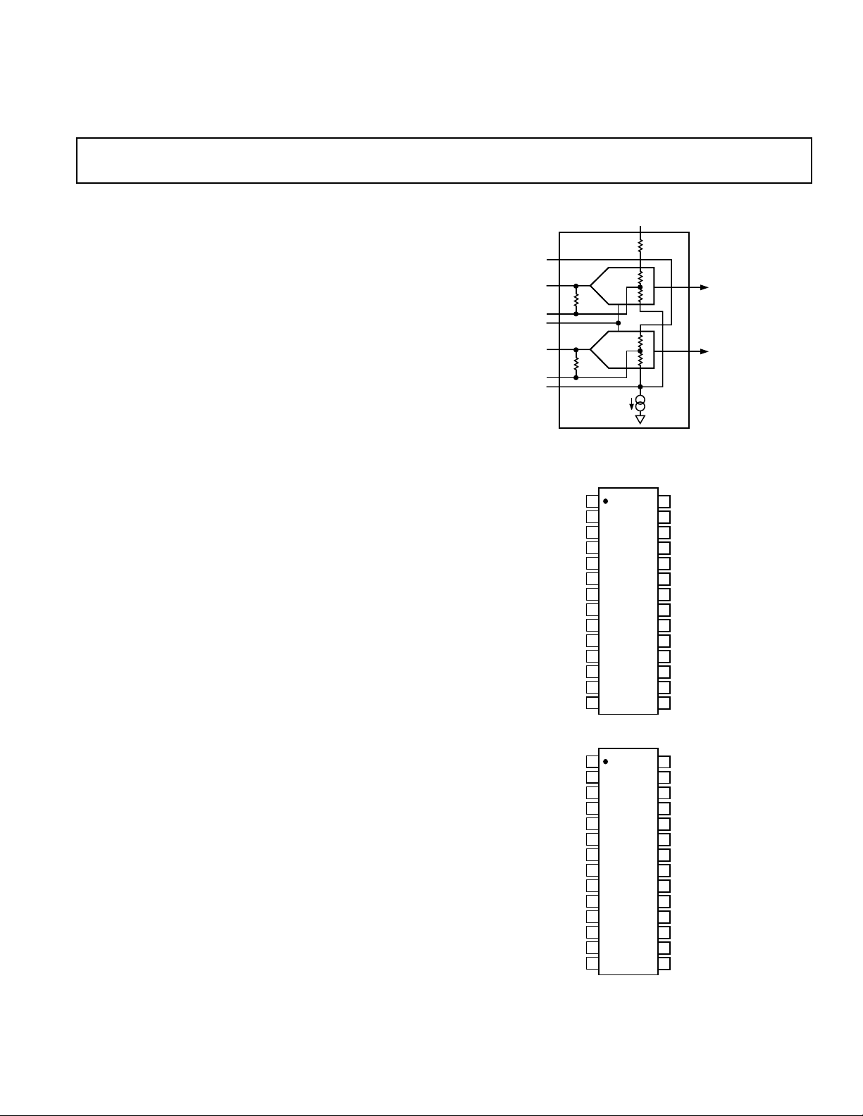
FUNCTIONAL BLOCK DIAGRAM
+V
S
AD9066
VT
INA
REF A
ENCODE
INB
REF B
VB
PIN CONFIGURATIONS
ENCODE D5A (MSB)
REF A D4B
REF B D2B
REF A
REF B
(LSB) D0B
(MSB) D5B
One Technology Way, P.O. Box 9106, Norwood, MA 02062-9106, U.S.A.
Tel: 781/329-4700 World Wide Web Site: http://www.analog.com
Fax: 781/326-8703 © Analog Devices, Inc., 2000
6-BIT
DAC
6-BIT
DAC
1
2
+V
S
3
GND D3A
4
GND D2A
5
+V
S
AD9066
6
INA D0A (LSB)
GND GND
+V
INB D3B
+V
INB
D1B
D2B
D3B
D4B
+V
(JR/AR)
7
TOP VIEW
(Not to Scale)
8
S
9
VT D5B (MSB)
10
11
12
13
VB D1B
14
NC D0B (LSB)
NC = NO CONNECT
1
S
2
VT
3
4
5
AD9066
6
VB
NC
(ARS)
7
TOP VIEW
(Not to Scale)
8
9
10
11
12
13
14
S
NC = NO CONNECT
28
D4A
27
26
25
D1A
24
23
22
+V
21
20
19
18
17
16
15
28
GND
27
INA
26
+V
25
GND
24
GND
+V
23
22
ENCODE
21
D5A (MSB)
20
D4A
19
D3A
18
D2A
17
D1A
16
D0A (LSB)
15
GND
S
S
S
D0A-D5A
D0B-D5B
Page 2

AD9066–SPECIFICATIONS
ELECTRICAL CHARACTERISTICS
(+VS = +5 V, AIN = 15.5 MHz, Encode Rate = 60 MSPS, TC = TA)
Test AD9066JR AD9066AR/ARS
Parameter Level Temp Min Typ Max Min Typ Max Unit
ANALOG INPUT
Full-Scale Input Range VI Full 475 500 525 450 500 530 mV
Gain Matching (FS Range) IV Full 16 16 mV
DC Input (Midscale)
Input Offset
1
1
V +25°C+V
– 1.1 +VS – 1.1 V
S
VI Full –1.0 +1.0 –1.0 +1.0 LSBs
Input Capacitance IV Full 10 15 10 15 pF
Input Resistance (DC) VI Full 25 45 55 22 45 57 kΩ
Input Bandwidth (3 dB) V +25°C 100 100 MHz
Gain Flatness (to 15 MHz) V +25°C 0.25 0.25 dB
Integral Linearity VI Full –1.0 +1.0 –1.0 +1.0 LSBs
Differential Linearity VI Full –0.5 +0.5 –0.5 +0.5 LSBs
Monotonicity VI Full Guaranteed Guaranteed
SWITCHING PERFORMANCE
Max Conversion Rate VI Full 60 60 MSPS
Output Delay (t
Output Delay (t
V
PD
2
)
2
)
IV Full 4 4 ns
IV Full 11 12 ns
Aperture Uncertainty (Jitter) V +25°C 10 10 ps rms
Aperture Time (tA) V +25°C 1.0 1.0 ns
DYNAMIC PERFORMANCE
3
Effective Number of Bits VI +25°C 5.3 5.7 5.2 5.7 Bits
SINAD VI +25°C3436 3336 dB
Harmonic Distortion (THD) VI +25°C4050 4050 dB
Crosstalk Rejection IV +25°C4050 4050 dBc
ENCODE INPUT
Logic High Voltage VI Full 2.0 2.0 V
Logic Low Voltage VI Full 0.8 0.8 V
Input High Current VI Full 500 500 µA
Input Low Current VI Full 500 500 µA
Pulsewidth High IV Full 7.0 7.0 ns
Pulsewidth Low IV Full 7.0 7.0 ns
DIGITAL OUTPUTS
Output Coding Full Offset Binary Offset Binary
Logic High Voltage (I
= 1 mA) VI Full 3.8 3.8 V
OH
Logic Low Voltage (IOL = 1 mA) VI Full 0.4 0.4 V
POWER SUPPLY
+VS Supply Voltage VI Full 4.75 5.25 4.75 5.25 V
Power Supply Rejection Ratio
Supply Current VI Full 80 120 80 120 mA
+V
S
Power Dissipation
NOTES
1
For ac coupled applications, the ADC is internally biased to insure that the midpoint transition of the ADC is within the limits specified with no signal applied. For
dc coupled applications, the dc value of the midpoint transition voltage will track the supply voltage within the limits shown for dc input (midscale) plus the dc offset.
Power Supply Rejection Ratio (PSRR) refers to the variation of the input signal range (gain) to supply voltage.
2
tV and tPD are measured from the 1.4 V level of the Clock and the 50% level between VOHand VOL. The ac load on all the digital outputs during test is 10 pF (max),
the dc load will not exceed ± 40 µA.
3
Effective number of bits (ENOB) and THD are measured using a FFT with a pure sine wave analog input @ 15.5 MHz, 1 dB below full scale. ENOB is calculated by
ENOB = (SNR – 1.76 dB)/6.02; THD is measured from full scale to the sum of the second through seventh harmonic of the input.
4
Typical thermal impedance for the “R” style (SOIC) 28-lead package is: θJC = 4°C/W, θCA = 41°C/W, θJA = 45°C/W, and the “RS” style (SSOP) 28-lead package is:
θJC = 26.97°C/W, θCA = 51.61°C/W, θJA = 78.58°C/W.
Specifications subject to change without notice.
4
1
IV Full 110 130 110 130 mV/V
VI Full 400 600 400 600 mW
–2–
REV. A
Page 3
AD9066
WARNING!
ESD SENSITIVE DEVICE
ABSOLUTE MAXIMUM RATINGS
Pin Min Max Unit
ENCODE –0.5 +V
+V
S
7.0 V
INA, INB –0.5 +V
VT 2.5 +V
REF A, REF B –0.5 +V
VB 0.0 +V
S
S
S
S
S
V
V
V
V
V
D0–D5 Current OUT 20 mA
EXPLANATION OF TEST LEVELS
Test Level Description
I 100% Production Tested
II 100% Production Tested at +25°C, and
Sample Tested at Specified Temperatures
III Sample Tested Only
IV Parameter Is Guaranteed by Design
V Parameter Is Typical Value Only
VI 100% Tested at +25°C
DIE LAYOUT AND MECHANICAL INFORMATION
Die Dimensions . . . . . . . . . . . . . . . . . 132 × 68 × 21 (±1) mils
Pad Dimensions . . . . . . . . . . . . . . . . . . . . . . . . . . . . 4 × 4 mils
Metalization . . . . . . . . . . . . . . . . . . . . . . . . . . . . . . Aluminum
Backing . . . . . . . . . . . . . . . . . . . . . . . . . . . . . . . . . . . . . . None
Substrate Potential . . . . . . . . . . . . . . . . . . . . . . . . . . . Ground
Transistor Count . . . . . . . . . . . . . . . . . . . . . . . . . . . . . . 5,810
Passivation . . . . . . . . . . . . . . . . . . . . . . . . . . . . Silicon Nitride
Die Attach . . . . . . . . . . . . . . . . . . . . . . . . . . . . . . Silver Filled
Bond Wire . . . . . . . . . . . . . . . . . . . . . . . . . . . . . . . . . . . . Gold
ORDERING GUIDE
Model Temperature Range Package Option*
AD9066AR –40°C to +85°C R-28
AD9066JR 0°C to +70°C R-28
AD9066ARS –40°C to +85°C RS-28
*R = “SO” Small Outline Package; RS = SSOP.
PIN DESCRIPTIONS
AR:JR ARS
Pin Pin
No. No. Name Function
1 22 ENCODE TTL Compatible CMOS Clock,
Samples on Rising Edge.
223+V
S
+5 V Supply for Digital Input.
3 24 GND Ground.
4 25 GND Ground.
526+V
S
+5 V Supply (Analog).
6 27 INA Channel A Analog Input.
7 28 GND Ground.
81+V
S
+5 V Supply (Analog).
9 2 VT Top of Voltage Reference, Bypass
to GND.
10 3 REF A Mid Reference to ADC A, Bypass
to GND.
11 4 INB Channel B Analog Input.
12 5 REF B Mid Reference to ADC B, Bypass
to GND.
13 6 VB Bottom of Reference Ladder, By-
pass to GND.
14 7 NC No Connect.
15 8 D0B (LSB) Digital Outputs Channel B,
CMOS Compatible.
16 9 D1B
17 10 D2B
18 11 D3B
19 12 D4B
20 13 D5B (MSB)
21 14 +V
S
+5 V Supply for Digital Outputs.
22 15 GND Ground.
23 16 D0A (LSB) Digital Outputs Channel A,
CMOS Compatible.
24 17 D1A
25 18 D2A
26 19 D3A
27 20 D4A
28 21 D5A (MSB)
CAUTION
ESD (electrostatic discharge) sensitive device. Electrostatic charges as high as 4000 V readily
accumulate on the human body and test equipment and can discharge without detection.
Although the AD9066 features proprietary ESD protection circuitry, permanent damage may
occur on devices subjected to high-energy electrostatic discharges. Therefore, proper ESD
precautions are recommended to avoid performance degradation or loss of functionality.
REV. A
–3–
Page 4

AD9066
5.8
5.7
5.6
5.5
ENOB – Bits
5.4
5.3
5.2
1
ENCODE = 60MSPS
10 100
MHz
Figure 1. ENOB vs. Analog Input Frequency
5.8
5.7
5.6
5.5
ENOB – Bits
5.4
ANALOG INPUT = 10.1MHz
Gain Variation
The full-scale input range is established by the current through
the two matched resistor ladders (620 ohms each nominal). Therefore the gain of the ADC may be modified by forcing different
voltages across the top and bottom voltage taps (VT and VB).
The easiest way to increase the input range will be to force VB
to a lower voltage. Using an external amplifier, the voltage at VB
may be forced as low as 3.0 V (3.58 nominal). Using the previously described relationship for full scale and the internal
resistor ladder values, 3.0 V at VB will result in a nominal fullscale input range of 705 mV.
A larger input range can be established by taking the VT voltage
all the way to the supply voltage level while pulling VB to 3.0 V.
This would force a 2 V potential across the ladder and create a
full-scale input range of 1.6 V.
Greater flexibility and improved power supply rejection can be
achieved by forcing external voltage references at both the top
and bottom of the resistor ladder.
111111
n
2
–2 = 62
100000
011111
5.3
5.2
10 100
MHz
Figure 2. ENOB vs. Encode Rate
USING THE AD9066
Analog Input and Voltage References
The AD9066 is optimized to allow ac coupled inputs with a fullscale input range of 500 mV ± 5%. An LSB weight is approximately 8 mV. The full-scale input range is defined as the voltage
range that accommodates 2
n
– 2 codes of equally weighted LSBs
(between the first and last code transitions). For the AD9066
there are 32 codes above and below the midscale voltage of the
A see Figure 3).
The full-scale input range of the AD9066 is equal to 500/620 ×
(VT – VB), or nominally 500 mV. For dc coupled applications,
the REF A and REF B voltages can be used to feed back offset
compensation signals. This will allow the midscale transition
voltage of the ADCs to track supply and temperature variations.
In the event that offset correction signals are generated digitally,
the REF pins would not be required. Figure 4a shows the
equivalent circuit for the internal references. All component
tolerances are ± 25%.
000001
000000
–FULL-SCALE MIDSCALE +FULL-SCALE
Figure 3.
+V
= 5V
S
310⍀
310⍀
400⍀
310⍀
310⍀
2mA
REF A
INPUT
VT
40k⍀ 40k⍀
REF B
VB
a. Reference Circuit
V
S
OUTPUTS
c. Output Bits
Figure 4. Equivalent Circuits
1.4V THRESHOLD
b. Encode Input
V
S
40k⍀
REF
d. Analog Input
V
S
–4–
REV. A
Page 5

Timing
+
+
+
+
AD9066
6 BITS
6 BITS
ENCODE
INA
REF A
OR REF B
INB
1/2
AD712
2k⍀
1/2
AD712
1/2
AD812
1/2
AD812
866⍀
866⍀
2k⍀
866⍀
866⍀
866⍀
866⍀
–15V
+15V
The duty cycle of the encode clock for the AD9066 is critical in
obtaining rated performance of the ADC. Rated maximum and
minimum pulse widths should be maintained, especially for
sample rates greater than 40 MSPS.
The AD9066 provides latched data outputs with three pipeline
delays. The length and load on the output data lines should be
minimized to reduce power supply transients inside the AD9066
which might diminish dynamic performance.
AD9066
ANALOG
INPUT
ENCODE
D0–D5
N
t
VALID DATA
FOR N–3
t
A
V
VALID DATA
t
PD
FOR N–2
N + 1
DATA
CHANGING
N + 2
VALID DATA
FOR N–1
Figure 5. Timing Diagram
The data is invalid during the period between tV and tPD. This
period refers to the time required for the AD9066 to fully switch
between valid CMOS logic levels. When latching the output
data, be careful to observe latch setup and hold time restrictions
as well as this data invalid period when designing the system
timing.
Layout and Signal Care
To insure optimum performance, a single low impedance
ground plane is recommended. Analog and digital grounds
should be connected together at the AD9066. Analog and digital power supplies should be bypassed, at the device, to ground
through 0.1 µF ceramic capacitors.
The use of sockets may limit the dynamic performance of the
part and is not recommended except for prototype or evaluation
purposes.
Driving the AD9066 with a Bipolar Input
The analog input range of the AD9066 is between 3.7 V and
4.2 V. Because the input is offset, the normal method of driving
the analog input is to use a blocking capacitor between the analog source and the AD9066 analog input pins. In applications
where DC coupling must be employed, the simple circuit shown
in Figure 6 will take a bipolar input and offset it to the operating
range of the AD9066.
To offset the input, the midpoint voltage of the AD9066 is buffered off chip and then inverted with an AD712, a low input bias
current dual op amp. This inverted midpoint is then fed to a
–5–
summation amplifier that combines the bipolar input with the
inverted offset voltage. The summation amplifier is an AD812, a
wideband current feedback amplifier that provides good bandwidth and low distortion.
REV. A
Figure 6. Bipolar Input Using AD812 Drive for AD9066
Layout should follow high frequency/high speed design guidelines. In addition the capacitance around the inverting input to
the AD812 should be minimized through a tight layout and the
use of low capacitance chip resistors for gain setting.
Quadrature Receiver Using the AD9066
Although any type of input signal may be applied, the AD9066
has been optimized for low cost in-phase and quadrature (I and
Q) demodulators. Primary applications include digital direct
broadcast satellite applications where broadband quadrature
phase shift keying (QPSK) modulation is used. In these receivers
the recovered signal is separated into I and Q vector components
and digitized.
AD9066
LPF
90ⴗIF IN
LPF
VCO
ADC
ADC
VCO
Figure 7. Simplified Block Diagram
For data symbol rates less than 10 Mbaud, the AD607 IF/RF
receiver subsystem provides an ideal solution for the second
conversion stage of a complete receiver system. Figure 8 shows
the AD9066 and AD607 used together.
The AD607 accepts inputs as high as 500 MHz which may be
the output of the first IF stage or RF signals directly. The IF/RF
signal is mixed with the local oscillator to provide an IF frequency of 400 kHz to 22 MHz. This signal is filtered externally
and then amplified with an on-chip AGC before being synchronously demodulated with an on-chip PLL carrier recovery
circuit. The outputs are digitized with the AD9066. The digital
outputs may be processed with a DSP chip such as the ADSP2171, ADSP-21062, general purpose DSP or ASIC.
Page 6

AD9066
LOCAL
OSCILLATOR
–16dBM
10⍀
RF INPUT
(ANTENNA)
+
MIDPOINT
GENERATOR
AD607
BIAS
BIAS
CIRCUIT
BANDPASS
FILTER
330⍀
4.7F
330⍀
100nF
100nF
AGC VOLTAGE
+
Figure 8. Digitizer with AD607 Receiver Circuit
Theory of Operation
The AD9066 dual ADC employs a patented interpolated flash
architecture. This architecture enables 64 possible quantization
levels with only 32 comparator preamplifiers. This keeps input
capacitance to a minimum. The midpoint of the reference ladder is fed back to the analog input, allowing easy biasing of the
ADC to midscale for ac coupled applications.
As shown in Figure 4d, a simple resistor is used to provide the
reference ladder midpoint to the analog input. The high impedance MOS inputs of the comparators insure no static voltage
drop across the resistor. This eliminates the need for an active
buffer (and its inherent offsets) to set the reference midpoint at
the analog input.
CLOCK
1
28
CLKIN
27
26
VMID
10⍀
PTAT
VOLTAGE
AGC
DETECTOR
OPTIONAL
BPF
OR LPF
PLL
6
V
INA
0ⴗ
AD9066
90ⴗ
11
V
INB
RECEIVED SIGNAL
STRENGTH INDICATOR
A OUTPUTS
25
(INPHASE)
24
23
20
19
18
B OUTPUTS
17
(QUADRATURE)
16
15
The outputs of the comparators are converted to a 6-bit word
and converted to CMOS levels. The digital signals are latched at
six stages (two pipeline delays) in the signal path. The digital
outputs are CMOS with approximately equal rise and fall times.
The encode clock utilizes a CMOS input stage with TTLcompatible (1.4 V) thresholds. Internal clock buffers minimize
external clock drive requirements.
–6–
REV. A
Page 7

OUTLINE DIMENSIONS
Dimensions shown in inches and (mm).
28-Lead Small Outline Package
(R-28)
0.7125 (18.10)
0.6969 (17.70)
AD9066
28 15
1
PIN 1
0.0118 (0.30)
0.0040 (0.10)
0.311 (7.9)
0.078 (1.98)
0.068 (1.73)
0.0500
(1.27)
BSC
0.407 (10.34)
0.397 (10.08)
28 15
0.301 (7.64)
PIN 1
0.0192 (0.49)
0.0138 (0.35)
28-Lead SSOP
(RS-28)
14
0.1043 (2.65)
0.0926 (2.35)
SEATING
PLANE
141
0.07 (1.79)
0.066 (1.67)
0.2992 (7.60)
0.2914 (7.40)
0.4193 (10.65)
0.3937 (10.00)
0.0125 (0.32)
0.0091 (0.23)
0.212 (5.38)
0.205 (5.21)
0.0291 (0.74)
0.0098 (0.25)
8ⴗ
0ⴗ
ⴛ 45ⴗ
0.0500 (1.27)
0.0157 (0.40)
C2019–0–6/00 (rev. A) 00566
0.008 (0.203)
0.002 (0.050)
0.0256
(0.65)
BSC
0.015 (0.38)
0.010 (0.25)
SEATING
PLANE
0.009 (0.229)
0.005 (0.127)
8°
0°
0.03 (0.762)
0.022 (0.558)
PRINTED IN U.S.A.
REV. A
–7–
 Loading...