

Page 1
8-Bit
a
40 MSPS/60 MSPS/80 MSPS A/D Converter
FEATURES
8-Bit, Low Power ADC: 200 mW Typical
120 MHz Analog Bandwidth
On-Chip +2.5 V Reference and T/H
1 V p-p Analog Input Range
Single +5 V Supply Operation
+5 V or +3 V Logic Interface
Power-Down Mode: < 10 mW
Three Performance Grades (40 MSPS, 60 MSPS, 80 MSPS)
APPLICATIONS
Digital Communications (QAM Demodulators)
RGB & YC/Composite Video Processing
Digital Data Storage Read Channels
Medical Imaging
Digital Instrumentation
PRODUCT DESCRIPTION
The AD9057 is an 8-bit monolithic analog-to-digital converter
optimized for low cost, low power, small size, and ease of use.
With a 40 MSPS, 60 MSPS or 80 MSPS encode rates capability and full-power analog bandwidth of 120 MHz, the component is ideal for applications requiring excellent dynamic
performance.
To minimize system cost and power dissipation, the AD9057
includes an internal +2.5 V reference and a track-and-hold
circuit. The user must provide only a +5 V power supply and an
encode clock. No external reference or driver components are
required for many applications.
The AD9057’s encode input is TTL/CMOS compatible and the
8-bit digital outputs can be operated from +5 V or +3 V supplies.
A power-down function may be exercised to bring total consumption to < 10 mW. In power-down mode the digital outputs
are driven to a high impedance state.
Fabricated on an advanced BiCMOS process, the AD9057 is
available in a space saving 20-lead surface mount plastic package (20 SSOP) and is specified over the industrial (–40°C to
+85°C) temperature range.
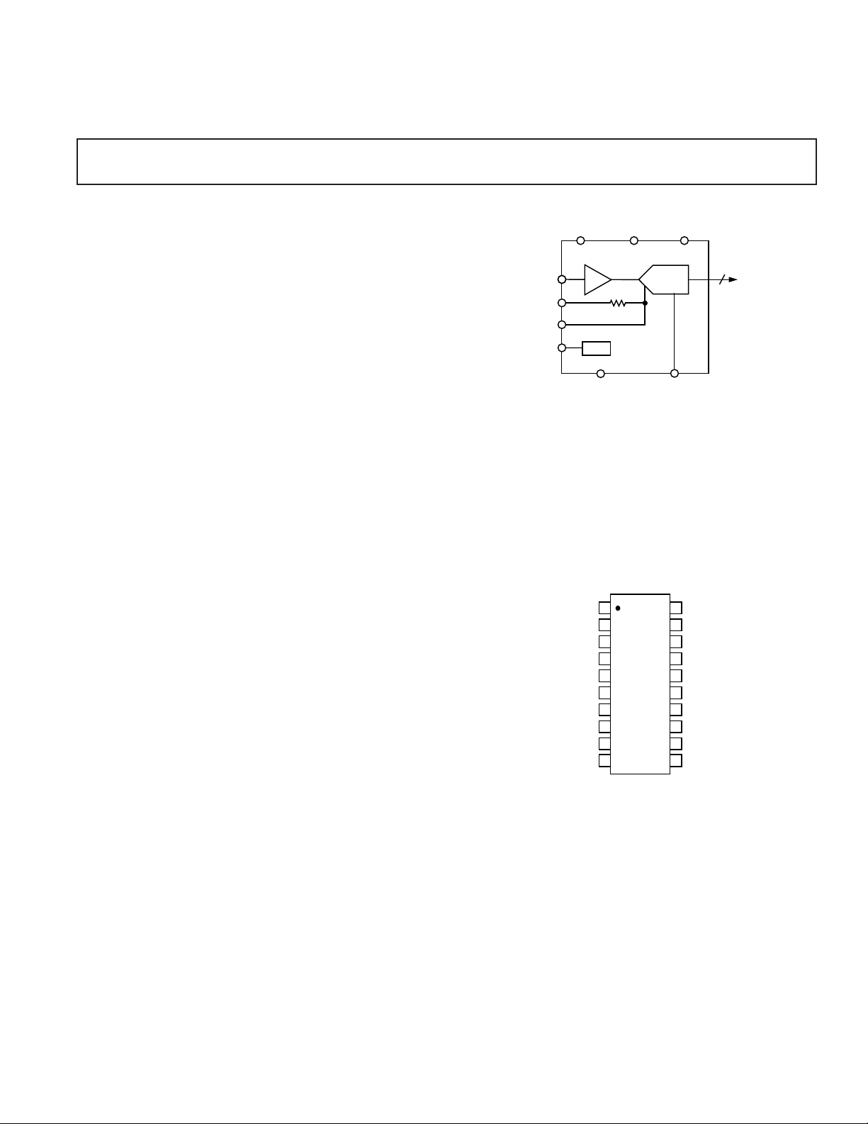
AD9057
FUNCTIONAL BLOCK DIAGRAM
V
AIN
BIAS OUT
VREF IN
VREF OUT
Customers desiring multichannel digitization may consider the
AD9059, a dual 8-bit, 60 MSPS monolithic based on the
AD9057 ADC core. The AD9059 is available in a 28-lead surface mount plastic package (28 SSOP) and is specified over the
industrial temperature range.
PIN CONFIGURATION
PWRDN
VREF OUT
VREF IN
BIAS OUT
ENCODE
D
+2.5V
GND
V
AIN
V
GND
AD9057
1kΩ
GND
1
2
3
4
5
D
6
7
8
D
9
10
(Not to Scale)
PWRDN V
ADCT/H
ENCODE
AD9057
TOP VIEW
20
19
18
17
16
15
14
13
12
11
DD
D0 (LSB)
D1
D2
D3
GND
V
DD
D4
D5
D6
D7 (MSB)
8
D7–D0
REV. B
Information furnished by Analog Devices is believed to be accurate and
reliable. However, no responsibility is assumed by Analog Devices for its
use, nor for any infringements of patents or other rights of third parties
which may result from its use. No license is granted by implication or
otherwise under any patent or patent rights of Analog Devices.
One Technology Way, P.O. Box 9106, Norwood, MA 02062-9106, U.S.A.
Tel: 617/329-4700 World Wide Web Site: http://www.analog.com
Fax: 617/326-8703 © Analog Devices, Inc., 1997
Page 2

AD9057–SPECIFICA TIONS
(VD = +5 V, VDD = +3 V; external reference)
Parameter Temp Level Min Typ Max Min Typ Max Min Typ Max Units
Test AD9057BRS-40 AD9057BRS-60 AD9057BRS-80
RESOLUTION 8 8 8 Bits
DC ACCURACY
Differential Nonlinearity +25°C I 0.75 1.9 0.75 1.9 0.75 1.9 LSB
Full VI 2.0 2.0 2.0 LSB
Integral Nonlinearity +25°C I 0.75 1.9 0.75 1.9 0.75 1.9 LSB
Full VI 2.0 2.0 2.0 LSB
No Missing Codes Full VI GUARANTEED GUARANTEED GUARANTEED
Gain Error
Gain Tempco
1
1
+25°C I –6 –2.5 +6 –6 –2.5 +6 –6 –2.5 +6 % FS
Full VI –8 +8 –8 +8 –8 +8 % FS
Full V ±70 ±70 ±70 ppm/°C
ANALOG INPUT
Input Voltage Range
(Centered at +2.5 V) +25°C V 1.0 1.0 1.0 V p-p
Input Offset Voltage +25°C I –15 ±0 +15 –15 ±0 +15 –15 ±0 +15 mV
Full VI –25 +25 –25 +25 –25 +25 mV
Input Resistance +25°C V 150 150 150 kΩ
Input Capacitance +25°CV222pF
Input Bias Current +25°CI 616 616 616µA
Full VI 25 25 25 µA
Analog Bandwidth +25°C V 120 120 120 MHz
BANDGAP REFERENCE
Output Voltage Full VI 2.4 2.5 2.6 2.4 2.5 2.6 2.4 2.5 2.6 V
Temperature Coefficient Full V ±10 ±10 ±10 ppm/°C
SWITCHING PERFORMANCE
Maximum Conversion Rate Full VI 40 60 80 MSPS
Minimum Conversion Rate Full IV 5 5 5 MSPS
Aperture Delay (t
Aperture Uncertainty (Jitter) +25°C V 5 5 5 ps, rms
Output Valid Time (t
) +25°C V 2.7 2.7 2.7 ns
A
2
)
V
Full IV 4.0 6.6 4.0 6.6 4.0 6.6 ns
Output Propagation Delay (tPD)2Full IV 11.5 18.0 9.5 14.2 8.0 11.3 ns
DYNAMIC PERFORMANCE
3
Transient Response +25°CV999ns
Overvoltage Recovery Time +25°CV999ns
Signal-to-Noise Ratio (SINAD)
(With Harmonics)
= 10.3 MHz +25°C I 42 45.5 42 45 41.5 45 dB
f
IN
= 76 MHz +25°C V 44.0 43.5 43.5 dB
f
IN
Effective Number of Bits
= 10.3 MHz +25°C I 6.7 7.2 6.7 7.2 6.6 7.2 Bits
f
IN
= 76 MHz +25°C V 7.0 6.9 6.9 Bits
f
IN
Signal-to-Noise Ratio (SNR)
(Without Harmonics)
= 10.3 MHz +25°C I 43 46.5 43 46 42.5 46 dB
f
IN
= 76 MHz +25°C V 45.5 45 45 dB
f
IN
2nd Harmonic Distortion
= 10.3 MHz +25°C I –50 –62 –50 –62 –50 –62 dBc
f
IN
= 76 MHz +25°C V –54 –54 –54 dBc
f
IN
3rd Harmonic Distortion
= 10.3 MHz +25°C I –46 –60 –46 –60 –46 –60 dBc
f
IN
= 76 MHz +25°C V –54 –54 –54 dBc
f
IN
Two Tone Intermodulation
Distortion (IMD) +25°C V –52 –52 –52 dBc
Differential Phase +25°C V 0.8 0.8 0.8 Degrees
Differential Gain +25°C V 1.0 1.0 1.0 %
DIGITAL INPUTS
Logic “1” Voltage Full VI 2.0 2.0 2.0 V
Logic “0” Voltage Full VI 0.8 0.8 0.8 V
Logic “1” Current Full VI ±1 ±1 ±1 µA
Logic “0” Current Full VI ±1 ±1 ±1 µA
Input Capacitance +25°C V 4.5 4.5 4.5 pF
Encode Pulse Width High (t
) +25°C IV 9.0 166 6.7 166 5.5 166 ns
EH
Encode Pulse Width Low (tEL) +25°C IV 9.0 166 6.7 166 5.5 166 ns
–2–
REV. B
Page 3
AD9057
Parameter Temp Level Min Typ Max Min Typ Max Min Typ Max Units
Test AD9057BRS-40 AD9057BRS-60 AD9057BRS-80
DIGITAL OUTPUTS
Logic “1” Voltage (V
= +3 V) Full VI 2.95 V
DD
Logic “1” Voltage (VDD = +5 V) Full IV 4.95 V
Logic “0” Voltage Full VI 0.05 V Output Coding
Offset Binary Code
POWER SUPPLY
V
Supply Current (VD = +5 V) Full VI 36 48 38 48 40 51 mA
D
VDD Supply Current (VDD = +3 V)4Full VI 4.0 6.5 5.5 6.5 7.4 8.8 mA
Power Dissipation
5, 6
Full VI 192 260 205 260 220 281 mW
Power-Down Dissipation Full VI 6 10 6 10 6 10 mW
Power Supply Rejection Ratio
(PSRR) +25°C I 15 15 15 mV/V
NOTES
1
Gain error and gain temperature coefficient are based on the ADC only (with a fixed +2.5 V external reference).
2
tV and tPD are measured from the 1.5 V level of the ENCODE to the 10%/90% levels of the digital output swing. The digital output load during test is not to exceed
an ac load of 10 pF or a dc current of ±40 µA.
3
SNR/harmonics based on an analog input voltage of –0.5 dBFS referenced to a 1.0 V full-scale input range.
4
Digital supply current based on VDD = +3 V output drive with <10 pF loading under dynamic test conditions.
5
Power dissipation is based on specified encode and 10.3 MHz analog input dynamic test conditions (V
6
Typical thermal impedance for the RS style (SSOP) 20-pin package: θJC = 46°C/W, θCA = 80°C/W, θJA = 126°C/W.
= +5 V ± 5%, VDD = +3 V ± 5%).
D
Specifications subject to change without notice.
EXPLANATION OF TEST LEVELS
Test Level Description
I 100% Production Tested
II 100% Production Tested at +25°C and Sample
Tested at Specified Temperatures
III Sample Tested Only
IV Parameter is Guaranteed by Design and Char-
acterization Testing
V Parameter is a Typical Value Only
VI 100% Production Tested at +25°C; Guaran-
teed by Design and Characterization Testing
for Industrial Temperature Range
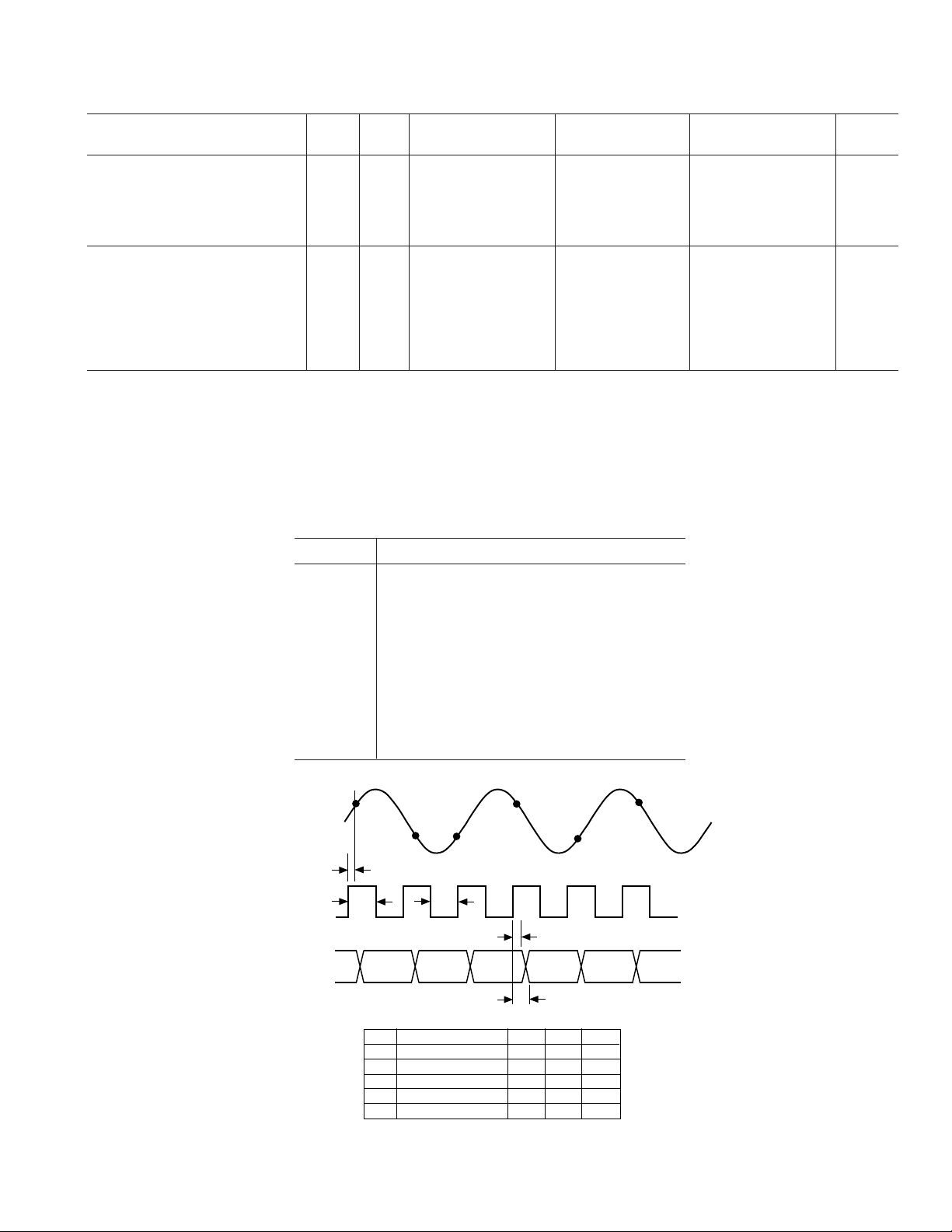
AIN
ENCODE
DIGITAL
OUTPUTS
N
N + 1
t
A
t
EH
N – 3 N – 2 N – 1 N N + 1 N + 2
N + 2
t
EL
N + 3
N + 4
t
V
t
PD
N + 5
REV. B
t
APERTURE DELAY
A
t
PULSE WIDTH HIGH
EH
t
PULSE WIDTH LOW
EL
t
V
OUTPUT VALID TIME
t
PD
OUTPUT PROP DELAY
Figure 1. Timing Diagram
–3–
MIN TYP MAX
2.7 ns
166 ns
166 ns
6.6 ns
4.0 ns
9.5 ns
Page 4
AD9057
WARNING!
ESD SENSITIVE DEVICE
ABSOLUTE MAXIMUM RATINGS
VD, VDD . . . . . . . . . . . . . . . . . . . . . . . . . . . . . . . . . . . . . +7 V
Analog Inputs . . . . . . . . . . . . . . . . . . . . –0.5 V to V
Digital Inputs . . . . . . . . . . . . . . . . . . . . –0.5 V to V
V
Input . . . . . . . . . . . . . . . . . . . . . . . –0.5 V to VD + 0.5 V
REF
+ 0.5 V
D
+ 0.5 V
DD
Digital Output Current . . . . . . . . . . . . . . . . . . . . . . . . 20 mA
Operating Temperature . . . . . . . . . . . . . . . –55°C to +125°C
Storage Temperature . . . . . . . . . . . . . . . . . –65°C to +150°C
Maximum Junction Temperature . . . . . . . . . . . . . . . . +175°C
Maximum Case Temperature . . . . . . . . . . . . . . . . . . +150°C
ORDERING GUIDE
Temperature
Model Range Package Option*
AD9057BRS–40, –60, –80 –40° C to +85°C RS-20
AD9057/PCB +25°C Evaluation Board
*RS = Shrink Small Outline (SSOP).
Table I. Digital Coding (VREF = +2.5 V)
Analog Input Voltage Level Digital Output
3.0 V Positive Full Scale 1111 1111
2.502 V Midscale +1/2 LSB 1000 0000
2.498 V Midscale –1/2 LSB 0111 1111
2.0 Negative Full Scale 0000 0000
PIN DESCRIPTIONS
Pin No. Name Function
1 PWRDN Power-Down Function Select;
Logic HIGH for Power-Down
Mode (Digital Outputs Go to
High Impedance State).
2 VREF OUT Internal Reference Output
(+2.5 V typ); Bypass with
0.1 µF to Ground.
3 VREF IN Reference Input for ADC (+2.5
V typ, ±10%).
4, 9, 16 GND Ground (Analog/Digital).
5, 8 V
D
Analog +5 V Power Supply.
6 BIAS OUT Bias Pin for AC Coupling
(1 kΩ to REF IN).
7 AIN Analog Input for ADC.
10 ENCODE Encode Clock for ADC (ADC
Samples on Rising Edge of
ENCODE).
11–14, 17–20 D7–D4, D3–D0 Digital Outputs of ADC.
15 V
DD
Digital Output Power Supply.
Nominally +3 V to +5
V.
PIN CONFIGURATION
PWRDN
VREF OUT
VREF IN
GND
BIAS OUT
AIN
GND
ENCODE
V
D
V
D
1
2
3
4
AD9057
5
TOP VIEW
(Not to Scale)
6
7
8
9
10
20
19
18
17
16
15
14
13
12
11
D0 (LSB)
D1
D2
D3
GND
V
DD
D4
D5
D6
D7 (MSB)
CAUTION
ESD (electrostatic discharge) sensitive device. Electrostatic charges as high as 4000 V readily
accumulate on the human body and test equipment and can discharge without detection.
Although the AD9057 features proprietary ESD protection circuitry, permanent damage may
occur on devices subjected to high energy electrostatic discharges. Therefore, proper ESD
precautions are recommended to avoid performance degradation or loss of functionality.
–4–
REV. B
Page 5

Typical Performance Characteristics–AD9057
ANALOG INPUT FREQUENCY – MHz
dB
–30
–70
0 16020 40 60 80 100 120 140
–35
–50
–55
–60
–65
–40
–45
ENCODE = 60MSPS
AIN = –0.5dBFS
3RD HARMONIC
2ND HARMONIC
0
–10
–20
–30
–40
dB
–50
–60
–70
–80
–90
030
Figure 2. Spectral Plot 60 MSPS, 10.3 MHz
0
ENCODE = 60MSPS
ANALOG IN = 76MHz, –0.5dBFS
–10
SINAD = 44.9dB
ENOB = 7.16 BITS
–20
SNR = 45.2dB
–30
–40
dB
–50
–60
–70
–80
–90
030
ENCODE = 60MSPS
ANALOG IN = 10.3MHz, –0.5dBFS
SINAD = 46.1dB
ENOB = 7.36 BITS
SNR = 46.5dB
FREQUENCY – MHz
FREQUENCY – MHz
Figure 5. Harmonic Distortion vs. AIN Frequency
0
–10
–20
–30
–40
dB
–50
–60
–70
–80
–90
03010 20
ENCODE = 60MSPS
F1 IN = 9.5MHz @ –7.0dBFS
F2 IN = 9.9MHz @ –7.0dBFS
2F1 - F2 = –52.0dBc
2F2 - F1 = –53.0dBc
FREQUENCY – MHz
Figure 3. Spectral Plot 60 MSPS, 76 MHz
48
46
44
42
40
dB
REV. B
ENCODE = 60MSPS
38
AIN = –0.5dBFS
36
34
32
30
0 16020 40 60 80 100 120 140
ANALOG INPUT FREQUENCY – MHz
Figure 4. SINAD/SNR vs. AIN Frequency
SINAD
SNR
–5–
Figure 6. Two-Tone Intermodulation Distortion
54
48
42
36
30
dB
AIN = 10.3MHz, –0.5dBFS
24
18
12
0
5 10 20304050607080 90
ENCODE RATE – MSPS
SNR
SINAD
Figure 7. SINAD/SNR vs. Encode Rate
Page 6

AD9057–
Typical Performance Characteristics
350
300
250
200
mW
150
100
AIN = 10.3MHz, –0.5dBFS
50
0
5 10 2030405060708090
ENCODE RATE – MSPS
VDD = +5V
VDD = +3V
Figure 8. Power Dissipation vs. Encode Rate
46.5
46.0
45.5
45.0
44.5
44.0
dB
43.5
43.0
42.5
42.0
41.5
–45 9002570
ENCODE = 60MSPS
AIN = 10.3MHz, –0.5dBFS
TEMPERATURE – °C
SNR
SINAD
12
11
10
9.5
9.0
8.5
– ns
PD
t
8.0
7.5
7.0
6.5
6.0
–45 9002570
Figure 11. t
46.5
46
45.5
45
44.5
dB
44
43.5
43
42.5
5.8 9.28.35
VDD = +3V
VDD = +5V
TEMPERATURE – °C
vs. Temperature/Supply (VDD = +3 V/+5 V)
PD
SNR
SINAD
ENCODE = 60MSPS
AIN = 10.3MHz, –05dBFS
ENCODE HIGH PULSE WIDTH –
10 10.96.7 7.5
ns
Figure 9. SINAD/SNR vs. Temperature
0
–0.2
–0.4
–0.6
–0.8
–1.0
GAIN ERROR – %
–1.2
–1.4
–1.6
–1.8
–45 9002570
TEMPERATURE – °C
Figure 10. ADC Gain vs. Temperature (with External
+2.5 V Reference)
Figure 12. SINAD/SNR vs. Encode Pulse Width
0
–1
–2
–3
–4
–5
–6
ADC GAIN – dB
–7
–8
–9
–10
1 10 100
ENCODE = 60MSPS
AIN = –0.5dBFS
2 5 20 50 200 500
ANALOG FREQUENCY – MHz
Figure 13. ADC Frequency Response
–6–
REV. B
Page 7

AD9057
THEORY OF OPERATION
The AD9057 combines Analog Devices’ proprietary MagAmp
gray code conversion circuitry with flash converter technology to
provide a high performance, low cost ADC. The design architecture ensures low power, high speed, and 8-bit accuracy. A
single-ended TTL/CMOS compatible ENCODE input controls
ADC timing for sampling the analog input pin and strobing the
digital outputs (D7–D0). An internal voltage reference (VREF
OUT) may be used to control ADC gain and offset or an external reference may be applied.
The analog input signal is buffered at the input of the ADC and
applied to a high speed track-and-hold. The T/H circuit holds
the analog input value during the conversion process (beginning
with the rising edge of the ENCODE command). The T/H’s
output signal passes through the gray code and flash conversion
stages to generate coarse and fine digital representations of the
held analog input level. Decode logic combines the multistage
data and aligns the 8-bit word for strobed outputs on the rising
edge of the ENCODE command. The MagAmp/Flash architecture of the AD9057 results in three pipeline delays for the output data.
USING THE AD9057
Analog Inputs
The AD9057 provides a single-ended analog input impedance of
150 kΩ. The input requires a dc bias current of 6 µA (typical)
centered near +2.5 V (±10%). The dc bias may be provided by
the user or may be derived from the ADC’s internal voltage
reference. Figure 14 shows a low cost dc bias implementation
allowing the user to capacitively couple ac signals directly into
the ADC without additional active circuitry. For best dynamic
performance, the VREF OUT pin should be decoupled to
ground with a 0.1 µF capacitor (to minimize modulation of
the reference voltage) and the bias resistor should be approximately 1 kΩ. A 1 kΩ bias resistor (±20%) is included within
the AD9057 and may be used to reduce application board size
and complexity.
+5V
2
REF OUT
REF IN
0.1µF
0.1µF
VIN
(1V p-p)
3
6
BIAS OUT
AIN
7
1kΩ
AD9057
Figure 14. Capacitively Coupled AD9057
Figure 15 shows typical connections for high performance dc
biasing using the ADC’s internal voltage reference. All components may be powered from a single +5 V supply (in the example
analog input signals are referenced to ground).
+5V
2
REF OUT
3
REF IN
AIN
7
AD9057
VIN
(–0.5V TO +0.5V)
1kΩ
+5V
10kΩ
AD8041
1kΩ
10kΩ
0.1µF
Figure 15. DC Coupled AD9057 (Inverted VIN)
Voltage Reference
A stable and accurate +2.5 V voltage reference is built into the
AD9057 (VREF OUT). The reference output may be used to
set the ADC gain/offset by connecting VREF OUT to VREF IN.
The internal reference is capable of providing 300µA of drive
current (for dc biasing the analog input or other user circuitry).
Some applications may require greater accuracy, improved
temperature performance, or gain adjustments which cannot be
obtained using the internal reference. An external voltage may
be applied to the VREF IN with VREF OUT disconnected for
gain adjustment of up to ±10% (the VREF IN pin is internally
tied directly to the ADC circuitry). ADC gain and offset will
vary simultaneously with external reference adjustment with a
1:1 ratio (a 2% or 50 mV adjustment to the +2.5 V reference
varies ADC gain by 2% and ADC input range center offset by
50 mV). Theoretical input voltage range versus reference input
voltage may be calculated from the following equations:
V
(p-p) = VREF IN/2.5
RANGE
V
MIDSCALE
V
TOP-OF-RANGE
V
BOTTOM-OF-RANGE
= VREF IN
= VREF IN + V
= VREF IN – V
RANGE
RANGE
/2
/2
Digital Logic (+5 V/+3 V Systems)
The digital inputs and outputs of the AD9057 can easily be
configured to interface directly with +3 V or +5 V logic systems.
The ENCODE and power-down (PWRDN) inputs are CMOS
stages with TTL thresholds of 1.5 V, making the inputs compatible with TTL, +5 V CMOS, and +3 V CMOS logic families.
As with all high speed data converters, the encode signal should
be clean and jitter free to prevent degradation of ADC dynamic
performance.
The AD9057’s digital outputs will also interface directly with
+5 V or +3 V CMOS logic systems. The voltage supply pin
(V
) for these CMOS stages is isolated from the analog V
DD
D
voltage supply. By varying the voltage on this supply pin the
digital output HIGH level will change for +5 V or +3 V systems.
Optimum SNR is obtained running the outputs at +3 V. Care
should be taken to isolate the V
supply voltage from the +5 V
DD
analog supply to minimize digital noise coupling into the ADC.
REV. B
–7–
Page 8

AD9057
The AD9057 provides high impedance digital output operation
when the ADC is driven into power-down mode (PWRDN,
logic HIGH). A 200 ns (minimum) power-down time should be
provided before a high impedance characteristic is required at
the outputs. A 200 ns power-up period should be provided to
ensure accurate ADC output data after reactivation (valid output
data is available three clock cycles after the 200 ns delay).
Timing
The AD9057 is guaranteed to operate with conversion rates
from 5 MSPS to 80 MSPS depending on grade. The ADC is
designed to operate with an encode duty cycle of 50%, but performance is insensitive to moderate variations. Pulse width variations of up to ±10% (allowing the encode signal to meet the
minimum/maximum HIGH/LOW specifications) will cause no
degradation in ADC performance (see Figure 1 timing diagram).
Power Dissipation
The power dissipation of the AD9057 is specified to reflect a
typical application setup under the following conditions: analog
input is –0.5 dBFS at 10.3 MHz, V
is +5 V, VDD is +3 V, and
D
digital outputs are loaded with 7 pF typical (10 pF maximum).
The actual dissipation will vary as these conditions are modified
in user applications. Figure 8 shows typical power consumption
for the AD9057 versus ADC encode frequency and V
supply
DD
voltage.
A power-down function allows users to reduce power dissipation
when ADC data is not required. A TTL/CMOS HIGH signal
(PWRDN) shuts down portions of the ADC and brings total
power dissipation to less than 10 mW. The internal bandgap
voltage reference remains active during power-down mode to
minimize ADC reactivation time. If the power-down function is
not desired, Pin 1 should be tied to ground.
APPLICATIONS
The wide analog bandwidth of the AD9057 makes it attractive
for a variety of high performance receiver and encoder applications. Figure 16 shows two ADCs in a typical low cost I & Q
demodulator implementation for cable, satellite, or wireless
LAN modem receivers. The excellent dynamic performance of
the ADC at higher analog input frequencies and encode rates
empowers users to employ direct IF sampling techniques (refer
to Figure 3 spectral plot). IF sampling eliminates or simplifies
analog mixer and filter stages to reduce total system cost and
power.
AD9057
AD9057
VCO
IF IN
90
VCO
BPF
°
BPF
Figure 16. I & Q Digital Receiver
The high sampling rate and analog bandwidth of the AD9057
are ideal for computer RGB video digitizer applications. With a
full-power analog bandwidth of 2× the maximum sampling
rate, the ADC provides sufficient pixel to pixel transient settling time to ensure accurate 60 MSPS video digitization. Figure 17 shows a typical RGB video digitizer implementation for
the AD9057.
RED
GREEN
BLUE
H-SYNC
AD9057
AD9057
AD9057
PLL
8
8
8
PIXEL CLOCK
Figure 17. RGB Video Encoder
Evaluation Board
The AD9057/PCB evaluation board provides an easy to use
analog/digital interface for the 8-bit, 60 MSPS ADC. The
board includes typical hardware configurations for a variety of
high speed digitization evaluations. On board components
include the AD9057 (in the 20-pin SSOP package), an optional
analog input buffer amplifier, a digital output latch, board
timing drivers, an analog reconstruction digital-to-analog converter, and configurable jumpers for ac coupling, dc coupling,
and power-down function testing. The board is configured at
shipment for dc coupling using the AD9057’s internal voltage
reference.
For dc coupled analog input applications, amplifier U2 is configured to operate as a unity gain inverter with adjustable offset
for the analog input signal. For full-scale ADC drive the analog
input signal should be 1 V p-p into 50 Ω (R1) referenced to
ground (0 V). The amplifier offsets the analog signal by
+VREF (+2.5 V typical) to center the voltage for proper ADC
input drive. For dc coupled operation, connect E1 to E2 (analog input to R2) and E11 to E12 (amplifier output to analog
input of AD9057) using the board jumper connectors. DC
offset of the analog input signal can be modified by adjusting
potentiometer R10.
For ac coupled analog input applications, amplifier U2 is
removed from the analog signal path. The analog signal is
coupled into the input of the AD9057 through capacitor C2.
The ADC pulls analog input bias current from the VREF IN
voltage through the 1 kΩ resistor internal to the AD9057
(BIAS OUT). The analog input signal to the board should be
1 V p-p into 50 Ω (R1) for full-scale ADC drive. For ac
coupled operation, connect E1 to E3 (analog input A to C2
feedthrough capacitor) and E10 to E12 (C2 to the analog input
and internal bias resistor) using the board jumper connectors.
The onboard reference voltage may be used to drive the ADC
or an external reference may be applied. To use the internal
voltage reference, connect E6 to E5 (VREF OUT to VREF
IN). To apply an external voltage reference, connect E4 to E5
(external reference from the REF banana jack to VREF IN).
The external voltage reference should be +2.5 V ± 10%.
–8–
REV. B
Page 9

AD9057
The power-down function of the AD9057 can be exercised
through a board jumper connection. Connect E7 to E9 (+5 V to
PWRDN) for power-down operation. For normal operation,
connect E8 to E9 (ground to PWRDN).
The encode signal source should be TTL/CMOS compatible
and capable of driving a 50 Ω termination (R7). The digital
outputs of the AD9057 are buffered through latches on the
evaluation board (U3) and are available for the user at connector Pins 30–37. Latch timing is derived from the ADC ENCODE clock and a digital clocking signal is provided for the
board user at connector Pins 2 and 21.
An onboard reconstruction digital-to-analog converter is
available for quick evaluations of ADC performance using an
+V
D
ENCODE
PWRDN
Digital Inputs
oscilloscope or spectrum analyzer. The DAC converts the
ADC’s digital outputs to an analog signal for examination at
the DAC OUT connector. The DAC is clocked at the ADC
ENCODE frequency. The AD9760 is a 10-bit/100 MSPS single
+5 V supply DAC. The reconstruction signal facilitates quick
system troubleshooting or confirmation of ADC functionality
without requiring external digital memory, timing, or display
interfaces. The DAC can be used for limited dynamic testing,
but customers should note that test results will be based on the
combined performance of the ADC and DAC (the best ADC
performance will be recognized by evaluating the digital outputs
of the ADC directly).
+V
D
AIN
500Ω
Analog Input
V
REFIN
, +3V TO +5V
+V
DD
D0–D7
Digital Outputs
+V
D
V
REFOUT
Output V
V
REF
Figure 18. Equivalent Circuits
V
REFIN
Bias Output
V
REFIN
1kΩ
REF
+V
D
Input
BIAS OUT
+V
D
3kΩ
2.5kΩ
REV. B
–9–
Page 10

AD9057
ANALOG IN
R1
50Ω
J7, V
E2
E1
DD
BNC
J1
E7
+5V
J6, REF
C17
DIS
+V
DD
NC
S
R7
50Ω
0.1µF
8
7
6
5
500Ω
R4
2kΩ
1
2
4
5
12
13
9
10
R10
U4
74AC00
U4
74AC00
U4
74AC00
U4
74AC00
R5
2kΩ
R6
10Ω
U2
ENCODE
C10
0.1µF
AD8041Q
1
NC
2
3
4
–V
BNC
J3
+
S
R3
1kΩ
C11
10µF
V
R2
1kΩ
E3
GND
E4
E5
E6
C1
E12
C2
0.1µF
GND
GND
0.1µF
E11
E10
3
6
11
8
E9
E8
+5V
+5V
PWRDN
1
PWRDN
2
REF OUT
3
REF IN
4
GND
5
V
D
6
BIAS OUT
7
AIN
8
V
D
9
GND
10
ENC
ANALOG
RECONSTRUCT
DAC OUT
(LSB) D0
(MSB) D7
DA7
DA6
DA5
DA4
DA3
DA2
DA1
DA0
GND
GND
BNC
J2
GND
V
10
D1
D2
D3
DD
D4
D5
D6
1
DB9
2
DB8
3
DB7
4
DB6
5
DB5
6
DB4
7
DB3
8
DB2
9
DB1
DB0
50Ω
20
D0
19
D1
18
D2
17
D3
16
GND
15
V
DD
14
D4
13
D5
12
D6
11
D7
28
CLK
(MSB)
(LSB)
IOUT
AB
22 21
R8
DAC
AD9760AR
DVDD
AVDD
COMP2
COMP1
FSADJ
REFIO
REFLO
SLEEP
R11
50Ω
C37DRPF
P2
DA0
DA1
DA2
DA3
DA4
DA5
DA6
DA7
1
2
3
4
5
6
7
8
9
10
11
12
13
14
15
16
17
18
19
20
21
22
23
24
25
26
27
28
29
30
31
32
33
34
35
36
37
U3
74ACQ574
9
D7
8
D6
7
D5
6
D4
5
D3
4
D2
3
D1
2
D0
27
24
23
19
18
17
16
15
8D
7D
6D
5D
4D
3D
2D
1D
+5V
+5V
CK
8Q
7Q
6Q
5Q
4Q
3Q
2Q
1Q
OE
111
C13
0.1µF
PWRDN
12
13
14
15
16
17
18
19
C18
0.1µF
R9
2kΩ
+5V
DA7
DA6
DA5
DA4
DA3
DA2
DA1
DA0
C19
0.1µF
J4, GND
J5, +5V
DECOUPLING CAPS
C3
0.1µF
C4
0.1µF
C7
0.1µF
C5
0.1µF
C8
0.1µF
C14
0.1µF
+
C9
0.1µF
C12
10µF
Figure 19. Evaluation Board Schematic
–10–
REV. B
Page 11

AD9057
REV. B
Figure 20. Evaluation Board Layout
–11–
Page 12

AD9057
OUTLINE DIMENSIONS
Dimensions shown in inches and (mm).
20-Lead SSOP
(RS-20)
0.295 (7.50)
0.271 (6.90)
20 11
0.311 (7.9)
0.301 (7.64)
0.078 (1.98)
0.068 (1.73)
0.008 (0.203)
0.002 (0.050)
PIN 1
0.0256
(0.65)
BSC
101
0.07 (1.78)
0.066 (1.67)
SEATING
PLANE
0.212 (5.38)
0.205 (5.21)
0.009 (0.229)
0.005 (0.127)
8°
0°
C2156b–2–4/97
0.037 (0.94)
0.022 (0.559)
–12–
PRINTED IN U.S.A.
REV. B
 Loading...