

Page 1
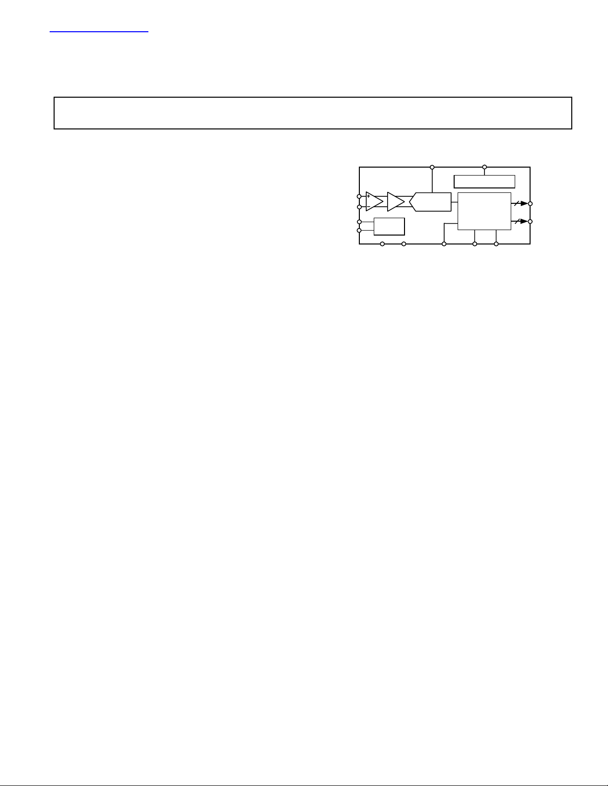
ENCODE
TIMING
ENCODE
AD9054
T/H
AIN
AIN
GND
12.5V REFERENCE
8
8
ENCODE
LOGIC
DEMULTIPLEXER
V
DD
DS
DS
DEMUX
QUANTIZER
VREF IN VREF OUT
DA7–DA
0
DB7–DB
0
查询AD9054供应商查询AD9054供应商
8-Bit, 200 MSPS
a
FEATURES
200 MSPS Guaranteed Conversion Rate
135 MSPS Low Cost Version Available
350 MHz Analog Bandwidth
1 V p-p Analog Input Range
Internal +2.5 V Reference and T/H
Low Power: 500 mW
+5 V Single Supply Operation
TTL Output Interface
Single or Demultiplexed Output Ports
APPLICATIONS
RGB Graphics Processing
High Resolution Video
Digital Data Storage Read Channels
Digital Communications
Digital Instrumentation
Medical Imaging
GENERAL DESCRIPTION
The AD9054 is an 8-bit monolithic analog-to-digital converter
optimized for high speed, low power, small size and ease of use.
With a 200 MSPS encode rate capability and full-power analog
bandwidth of 350 MHz, the component is ideal for applications
requiring the highest possible dynamic performance.
To minimize system cost and power dissipation, the AD9054
includes an internal +2.5 V reference and track-and-hold circuit.
The user provides only a +5 V power supply and an encode
clock. No external reference or driver components are required
for many applications.
A/D Converter
AD9054
FUNCTIONAL BLOCK DIAGRAM
The AD9054’s encode input interfaces directly to TTL, CMOS
or positive-ECL logic and will operate with single-ended or
differential inputs. The user may select dual-channel or singlechannel digital outputs. The dual (demultiplexed) mode interleaves ADC data through two 8-bit channels at one-half the
clock rate. Operation in demultiplexed mode reduces the speed
and cost of external digital interfaces while allowing the ADC to
be clocked to the full 200 MSPS conversion rate. In the singlechannel (nondemultiplexed) mode, all data is piped at the full
clock rate to the Channel A outputs.
Fabricated with an advanced BiCMOS process, the AD9054 is
provided in a space-saving 44-lead TQFP surface mount plastic
package (ST-44) and specified over the full industrial (–40°C to
+85°C) temperature range.
REV. 0
Information furnished by Analog Devices is believed to be accurate and
reliable. However, no responsibility is assumed by Analog Devices for its
use, nor for any infringements of patents or other rights of third parties
which may result from its use. No license is granted by implication or
otherwise under any patent or patent rights of Analog Devices.
One Technology Way, P.O. Box 9106, Norwood, MA 02062-9106, U.S.A.
Tel: 781/329-4700 World Wide Web Site: http://www.analog.com
Fax: 781/326-8703 © Analog Devices, Inc., 1997
Page 2

AD9054–SPECIFICA TIONS
ELECTRICAL CHARACTERISTICS
(VDD = +5 V, external reference, fS = max unless otherwise noted)
Test AD9054BST-200 AD9054BST-135
Parameter Temp Level Min Typ Max Min Typ Max Units
RESOLUTION 8 8 Bits
DC ACCURACY
Differential Nonlinearity +25°CI ±0.9 +1.5/–1.0 ±0.9 +1.5/–1.0 LSB
Full VI ±1.0 +2.0/–1.0 ±1.0 +2.0/–1.0 LSB
Integral Nonlinearity +25°CI ±0.6 ±1.5 ±0.6 ±1.5 LSB
Full VI ±0.9 ±2.0 ±0.9 ±2.0 LSB
No Missing Codes Full VI Guaranteed Guaranteed
Gain Error
Gain Tempco
1
1
+25°CI ±2 ±7 ±2 ±7% FS
Full V 160 160 ppm/ °C
ANALOG INPUT
Input Voltage Range
(With Respect to AIN) Full V ±512 ±512 mV p–p
Compliance Range AIN or AIN Full V 1.8 3.2 1.8 3.2 V
Input Offset Voltage +25°CI ±4 ±16 ±4 ±16 mV
Full VI ±8 ±19 ±8 ±19 mV
Input Resistance +25°C I 36 62 36 62 kΩ
Full VI 23 23 kΩ
Input Capacitance +25 °CV 4 4 pF
Input Bias Current +25°C I 25 50 25 50 µA
Analog Bandwidth, Full Power
2
Full VI 75 75 µA
+25°C V 350 350 MHz
REFERENCE OUTPUT
Output Voltage Full VI 2.4 2.5 2.6 2.4 2.5 2.6 V
Temperature Coefficient Full V 110 110 ppm/°C
SWITCHING PERFORMANCE
Maximum Conversion Rate (fS) Full VI 200 135 MSPS
Minimum Conversion Rate (f
Encode Pulsewidth High (t
Encode Pulsewidth Low (t
Aperture Delay (t
) +25°C V 0.5 0.5 ns
A
) Full IV 25 25 MSPS
S
) +25°C IV 2.0 15 3.0 15 ns
EH
) +25°C IV 2.0 15 3.0 15 ns
EL
Aperture Uncertainty (Jitter) +25°C V 2.3 2.3 ps rms
Data Sync Setup Time (t
Data Sync Hold Time (t
Data Sync Pulsewidth (t
Output Valid Time (t
Output Propagation Delay (tPD)
DIGITAL INPUTS
HIGH Level Current (IIH)
LOW Level Current (I
) +25°CIV 0 0 ns
SDS
) +25°C IV 0.5 0.5 ns
HDS
) +25 °C IV 2.0 2.0 ns
PWDS
3
)
V
IL
3
4
4
)
Full VI 2.7 5.1 2.7 5.7 ns
Full VI 5.9 7.9 7.5 8.5 ns
Full VI 500 625 500 625 µA
Full VI 500 625 500 625 µA
Input Capacitance +25 °CV 3 3 pF
DIFFERENTIAL INPUTS
Differential Signal Amplitude (VID) Full IV 400 400 mV
HIGH Input Voltage (V
LOW Input Voltage (V
IHD
ILD
Common-Mode Input (V
) Full IV 1.5 V
DD
) Full IV 0 VDD – 0.4 0 VDD – 0.4 V
) Full IV 1.5 1.5 V
ICM
1.5 V
DD
V
DEMUX INPUT
HIGH Input Voltage (VIH) Full IV 2.0 V
DD
2.0 V
DD
V
LOW Input Voltage (VIL) Full IV 0 0.8 0 0.8 V
DIGITAL OUTPUTS
HIGH Input Voltage (VOH) Full VI 2.4 2.4 V
LOW Input Voltage (V
) Full VI 0.4 0.4 V
OL
Output Coding Binary Binary
–2–
REV. 0
Page 3

AD9054
Test AD9054BST-200 AD9054BST-135
Parameter Temp Level Min Typ Max Min Typ Max Units
POWER SUPPLY
VDD Supply Current (IDD) Full VI 100 145 100 140 mA
Power Dissipation
5, 6
Full VI 500 725 500 700 mW
Power Supply Sensitivity
DYNAMIC PERFORMANCE
7
8
+25°C I 0.005 0.015 0.005 0.015 V/V
Transient Response +25°C V 1.5 1.5 ns
Overvoltage Recovery Time +25 °C V 1.5 1.5 ns
Signal-to-Noise Ratio (SNR)
(Without Harmonics)
fIN = 19.7 MHz +25°CIV 42 45 42 45 dB
Full V 45 45 dB
= 49.7 MHz +25°C I 42 45 42 45 dB
f
IN
Full V 45 45 dB
fIN = 70.1 MHz +25°C I 42 45 dB
Full V 45 dB
Signal-to-Noise Ratio (SINAD)
(With Harmonics)
= 19.7 MHz +25°CIV 40 43 40 43 dB
f
IN
Full V 43 43 dB
fIN = 49.7 MHz +25°C I 40 43 40 43 dB
Full V 43 43 dB
fIN = 70.1 MHz +25°C I 39 42 dB
Full V 42 dB
Effective Number of Bits
= 19.7 MHz +25°C IV 6.35 6.85 6.35 6.85 Bits
f
IN
= 49.7 MHz +25°C I 6.35 6.85 6.35 6.85 Bits
f
IN
= 70.1 MHz +25°C I 6.18 6.85 Bits
f
IN
2nd Harmonic Distortion
fIN = 19.7 MHz +25°C IV 58 63 58 63 dBc
= 49.7 MHz +25°C I 54 59 54 59 dBc
f
IN
f
= 70.1 MHz +25°C I 52 55 dBc
IN
3rd Harmonic Distortion
= 19.7 MHz +25°C IV 48 56 48 56 dBc
f
IN
f
= 49.7 MHz +25°C I 48 54 48 54 dBc
IN
= 70.1 MHz +25°C I 43 50 dBc
f
IN
Two-Tone Intermod Distortion
(IMD)
= 19.7 MHz +25°C V 60 60 dBc
f
IN
= 49.7 MHz +25°C V 55 55 dBc
f
IN
fIN = 70.1 MHz +25°C V 50 dBc
NOTES
1
Gain error and gain temperature coefficient are based on the ADC only (with a fixed +2.5 V external reference).
2
3 dB bandwidth with full-power input signal.
3
tV and tPD are measured from the threshold crossing of the ENCODE input to valid TTL levels of the digital outputs. The output ac load during test is 5 pF (Refer to
equivalent circuits Figures 5 and 6).
4
IIH and IIL are valid for differential input voltages of less than 1.5 V. At higher differential voltages, the input current will increase to a maximum of 1.25 mA.
5
Power dissipation is measured under the following conditions: analog input is –1 dBfs at 19.7 MHz.
6
Typical thermal impedance for the ST-44 (TQFP) 44–lead package (in still air): θJC = 20°C/W, θCA = 35°C/W, θJA = 55°C/W.
7
A change in input offset voltage with respect to a change in VDD.
8
SNR/harmonics based on an analog input voltage of –1.0 dBfs referenced to a 1.024 V full–scale input range.
Specifications subject to change without notice.
EXPLANATION OF TEST LEVELS
Test Level
I. 100% production tested.
II. 100% production tested at +25°C and sample tested at
specified temperatures.
III. Sample tested only.
IV. Parameter is guaranteed by design and characterization testing.
V. Parameter is a typical value only.
VI. 100% production tested at +25°C; guaranteed by design
and characterization testing for industrial temperature range.
–3–REV. 0
Page 4
AD9054
WARNING!
ESD SENSITIVE DEVICE
ABSOLUTE MAXIMUM RATINGS*
VDD . . . . . . . . . . . . . . . . . . . . . . . . . . . . . . . . . . . . . . . . +6 V
Analog Inputs . . . . . . . . . . . . . . . . . . . . . . . . . . V
Digital Inputs . . . . . . . . . . . . . . . . . . . . . . . . . . V
VREF IN, VREF OUT . . . . . . . . . . . . . . . . . . . V
to 0.0 V
DD
to 0.0 V
DD
to 0.0 V
DD
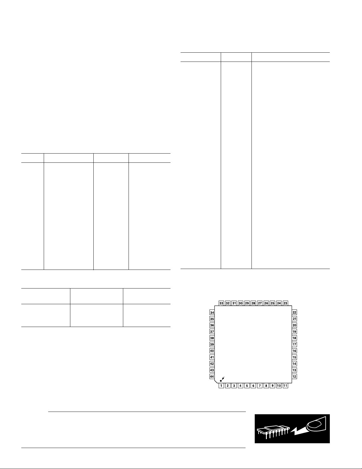
Pin Number Name Function
1 ENCODE Encode Clock for ADC (ADC
Digital Output Current . . . . . . . . . . . . . . . . . . . . . . . . 20 mA
Operating Temperature . . . . . . . . . . . . . . . . –55°C to +125°C
Storage Temperature . . . . . . . . . . . . . . . . . . –65°C to +150°C
2 ENCODE Encode Clock Complement
Maximum Junction Temperature . . . . . . . . . . . . . . . +175°C
Maximum Case Temperature . . . . . . . . . . . . . . . . . . +150°C
*Stresses above those listed under Absolute Maximum Ratings may cause perma-
nent damage to the device. This is a stress rating only; functional operation of the
device at these or any other conditions outside of those indicated in the operation
sections of this specification is not implied. Exposure to absolute maximum ratings
for extended periods may affect device reliability.
3, 5, 15, 18, 28, VDD Power Supply (+5 V).
30, 31, 36, 41
4, 6, 16, 17, 27, GND Ground.
29, 32, 35, 37, 40
14–7 DA
Table I. Output Coding
19–26 DB
Step AIN–AIN Code Binary
255 ≥0.512 V 255 1111 1111
33 VREF OUT Internal Reference Output
254 0.508 V 254 1111 1110
253 0.504 V 253 1111 1101
•• • •
34 VREF IN Reference Input for ADC (+2.5 V
•• • •
•• • •
38 AIN Analog Input—Complement.
129 0.006 V 129 1000 0001
128 0.002 V 128 1000 0000
127 –0.002 V 127 0111 1111
126 –0.006 V 126 0111 1110
•• • •
39 AIN Analog Input—True.
42 DEMUX Format Select. LOW = Dual.
•• • •
•• • •
2 –0.504 V 2 0000 0010
1 –0.508 V 1 0000 0001
43 DS Data Sync Complement.
44 DS Data Sync—Aligns output chan-
0 ≤–0.512 V 0 0000 0000
ORDERING GUIDE
Temperature Package
Model Range Option*
AD9054BST-200 –40°C to +85°C ST-44
AD9054BST-135 –40°C to +85°C ST-44
AD9054/PCB +25°C Evaluation Board
*ST = Plastic Thin Quad Flatpack (TQFP).
VREF IN
GND
VDD
GND
AIN
AIN
GND
VDD
DEMUX
DS
PIN FUNCTION DESCRIPTIONS
Samples on Rising Edge of
ENCODE).
(ADC Samples on Falling Edge
of ENCODE).
–DA
0
–DB
0
Digital Outputs of ADC Channel
7
A. DA
is the MSB, DA0 the LSB.
7
Digital Outputs of ADC Channel
7
B. DB
is the MSB, DB0 the LSB.
7
(+2.5 V typical); Bypass with
0.1 µF to Ground.
typical, ±4%).
Connect to input signal midscale
reference.
Channel Mode, HIGH = Single.
Channel Mode (Channel A Only).
nels in Dual-Channel Mode.
PIN CONFIGURATION
(MSB)
6DB5DB4
7
DB
VREF OUT
GND
VDD
GND
VDD
VDD
AD9054
TOP VIEW
(PINS DOWN)
DS
PIN 1
IDENTIFIER
GND
DB
DB
3
DB
2
DB
1
DB
(LSB)
0
VDD
GND
GND
VDD
DA0 (LSB)
DA
1
DA
2
CAUTION
ESD (electrostatic discharge) sensitive device. Electrostatic charges as high as 4000 V readily
accumulate on the human body and test equipment and can discharge without detection.
Although the AD9054 features proprietary ESD protection circuitry, permanent damage may
occur on devices subjected to high energy electrostatic discharges. Therefore, proper ESD
precautions are recommended to avoid performance degradation or loss of functionality.
–4–
ENCODE
ENCODE
VDD
GND
VDD
GND
6DA5DA4DA3
DA
(MSB)
7
DA
REV. 0
Page 5
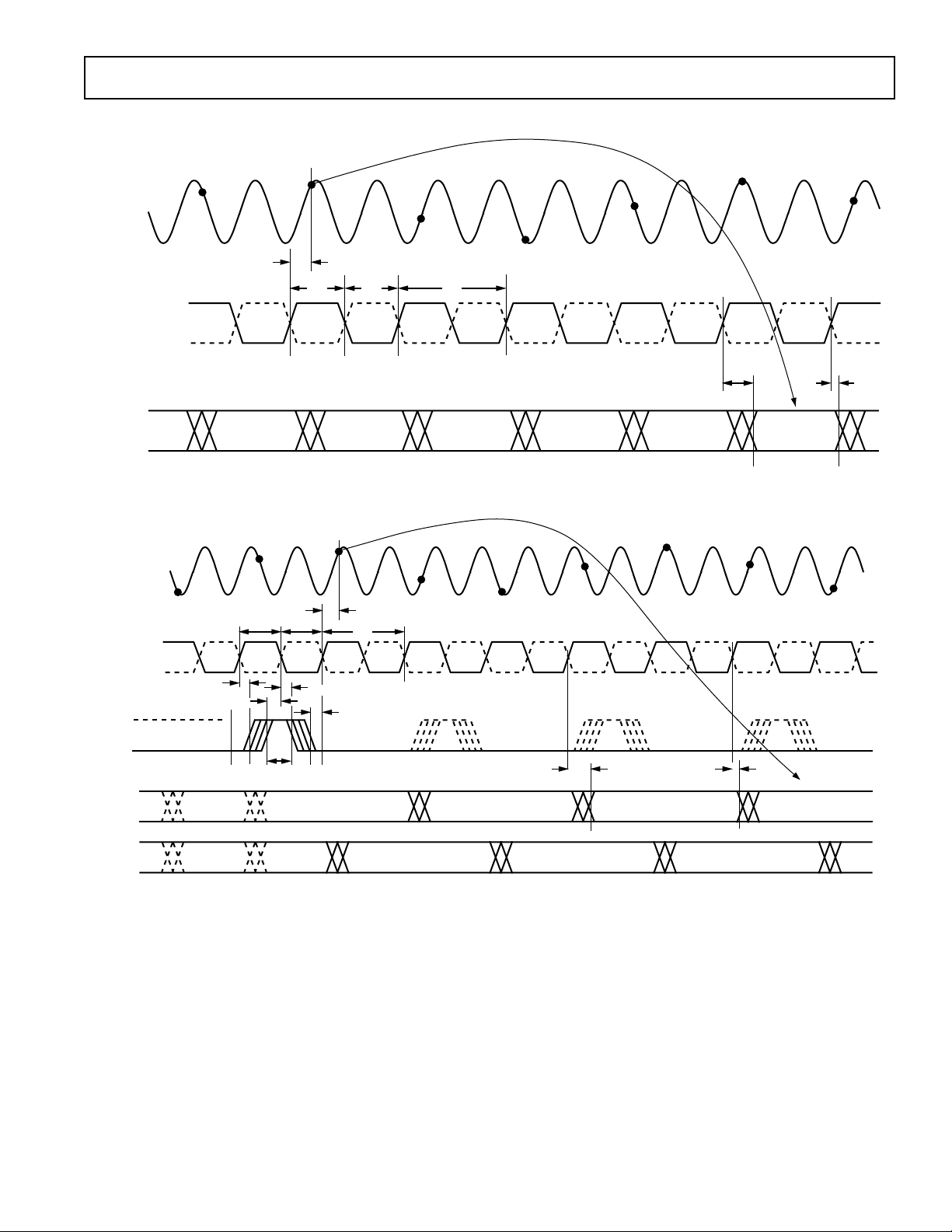
AD9054
AIN
ENCODE
ENCODE
D
7–D0
AIN
ENCODE
SAMPLE N–1
SAMPLE N–1
t
EH
SAMPLE N SAMPLE N+3 SAMPLE N+4
t
A
t
EH
t
EL
1/f
S
SAMPLE N+2SAMPLE N+1
t
DATA N–2DATA N–3DATA N–4DATA N–5
Figure 1. Timing—Single Channel Mode
t
EL
SAMPLE N
t
A
1/f
S
SAMPLE N+3 SAMPLE N+4 SAMPLE N+5
PD
t
V
DATA NDATA N–1
SAMPLE N+6SAMPLE N+2SAMPLE N+1SAMPLE N–2
ENCODE
DS
DS
PORT A
D7–D
PORT B
D
7–D0
t
HDS
t
SDS
DATA N–7
0
OR N–8
DATA N–8
OR N–7
t
PWDS
DATA N–6
OR N–7
t
HDS
DATA N–7
OR N–6
t
SDS
INVALID IF OUT OF SYNC
DATA N–5 IF IN SYNC
INVALID IF OUT OF SYNC
DATA N–4 IF IN SYNC
t
PD
DATA N–2
DATA N–3 DATA N–1
t
V
DATA N
DATA N+1
Figure 2. Timing—Dual Channel Mode
–5–REV. 0
Page 6
AD9054
V
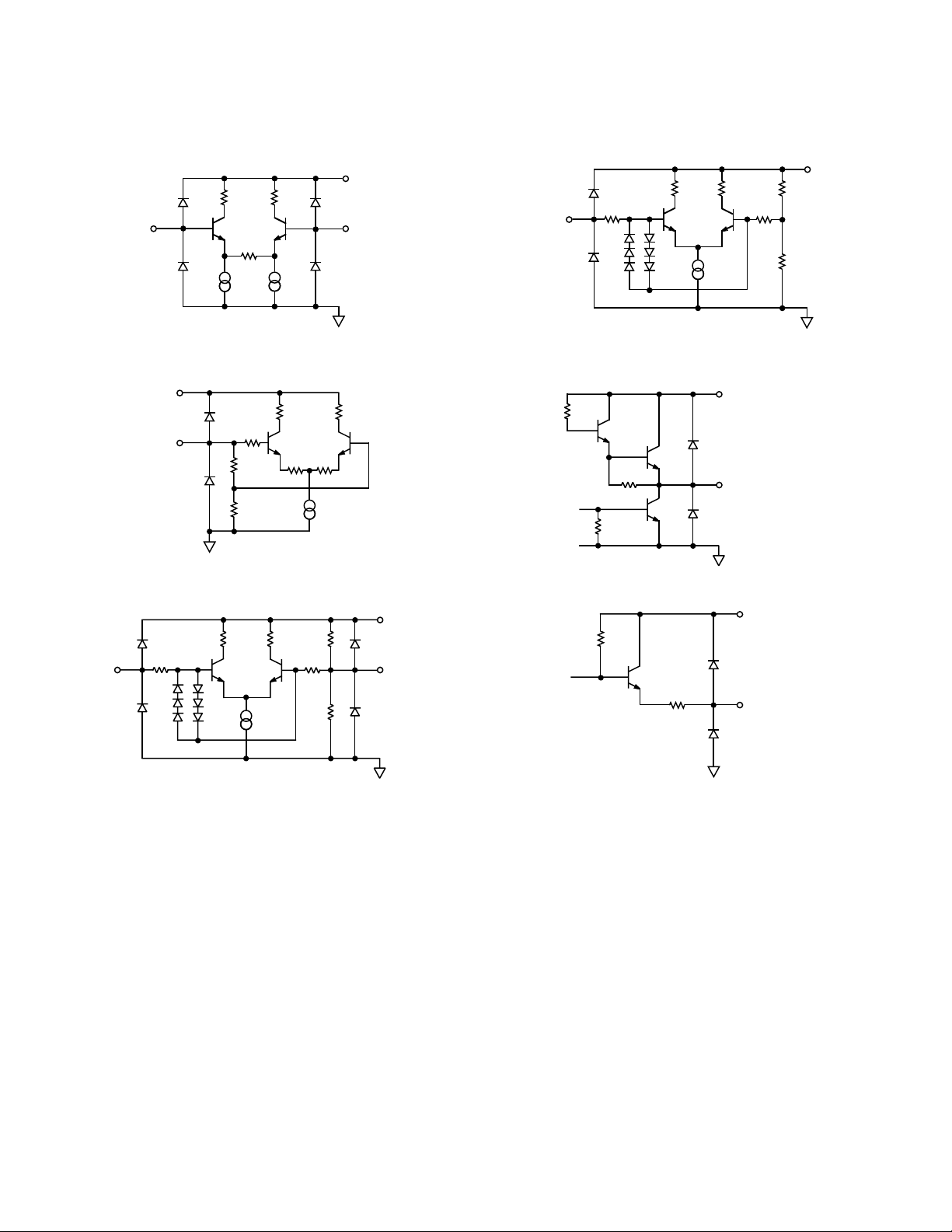
EQUIVALENT CIRCUITS
AIN
Figure 3. Equivalent Analog Input Circuit
V
DD
VREF IN
Figure 4. Equivalent Reference Input Circuit
17.5kV
ENCODE
OR DS
300V
300V
7.5kV
V
AIN
7.5kV
V
DD
DD
DEMUX
Figure 6. Equivalent
300V 300V
DEMUX
17.5kV
Input Circuit
V
DD
DIGITAL
OUTPUTS
Figure 7. Equivalent Digital Output Circuit
V
DD
ENCODE
OR DS
DD
VREF
OUT
Figure 5. Equivalent ENCODE and Data Select Input Circuit
–6–
Figure 8. Equivalent Reference Output Circuit
REV. 0
Page 7

55
dB
TC – 8C
44.0
–45
0
25 70 90
45.2
44.8
44.4
44.2
45.4
45.0
44.6
70MHz
20MHz
50MHz
dB
TC – 8C
46.0
44.0
–60 100–40 –20 0 20 40 60 80
45.8
45.2
44.8
44.4
44.2
45.6
45.4
45.0
44.6
20MHz
50MHz
70MHz
50
SNR
45
dB
40
35
30
0 14020 40 60 80 100 120
SINAD
NYQUIST
FREQUENCY
(100MHz)
fIN – MHz
Typical Performance Characteristics–
AD9054
Figure 9. SNR vs. fIN:fS = 200 MSPS
50
49
48
47
46
45
dB
44
43
42
41
40
25 50 100 150 200 250 300
75 125 175 225 270
Figure 10. SNR vs. fS: fIN = 19.7 MHz
50
45
40
35
dB
30
25
20
25
75 125 175 225 270
50 100 150 200 250 300
Figure 11. SNR vs. fS:fIN = 70.1 MHz
SINAD
fS – MSPS
SINAD
fS – MSPS
SNR
SNR
Figure 12. SNR vs. Temperature, fS = 135 MSPS
Figure 13. SNR vs. Temperature, fS = 200 MSPS
50
FS = 135MSPS
48
= 10.3MHz
F
IN
46
44
42
40
dB
38
36
34
32
30
0.0 8.01.0 2.0 3.0 4.0 5.0 6.0 7.0
ENCODE PULSEWIDTH – ns
Figure 14. SNR vs. Clock Pulsewidth, (t
–7–REV. 0
SNR
SINAD
): fS = 135 MSPS
PWH
Page 8

AD9054
50
FS = 200MSPS
48
= 10.3MHz
F
IN
46
44
42
40
dB
38
36
34
32
30
0.0 5.00.5 1.0 1.5 2.0 2.5 3.0 3.5 4.0 4.5
ENCODE PULSEWIDTH – ns
Figure 15. SNR vs. Clock Pulsewidth, (t
46
45
44
43
42
dB
41
40
39
38
–60 100–40 –20 0 20 40 60 80
TC – 8C
SNR
SINAD
70MHz
): fS = 200 MSPS
PWH
50MHz
Figure 16. SINAD vs. Temperature: fS = 135 MSPS
20MHz
–70
–68
–66
–64
–62
–60
–58
dBc
–56
–54
–52
–50
–48
–46
25 22550 100 150 200 250 300
2ND HARMONIC
3RD HARMONIC
75 125 175 270
fS – MSPS
Figure 18. Harmonic Distortion vs. fS:fIN = 19.7 MHz
–60
–50
–40
–30
–20
–10
2ND HARMONIC
3RD HARMONIC
0
25
50 100 150 225 27075 125 175 200 250
f
– MSPS
S
300
Figure 19. Harmonic Distortion vs. fS:fIN = 70.1 MHz
46
45
44
43
42
dB
41
40
39
38
–60 100–40 –20 0 20 40 60 80
70MHz
TC – 8C
20MHz
50MHz
Figure 17. SINAD vs. Temperature: fS = 200 MSPS
–40
–45
–50
–55
dB
–60
–65
–70
–60 100–40 –20 0 20 40 60 80
70MHz
50MHz
20MHz
TC – 8C
Figure 20. 2nd Harmonic vs. Temperature: fS = 135 MSPS
–8–
REV. 0
Page 9

AD9054
MHz
dB
0 10010 20 30 40 50 60 70 80 90
0
–10
–90
–50
–60
–70
–80
–30
–40
–20
FUNDAMENTAL = –0.5dBfs
SNR = 45.8dB
SINAD = 45.2dB
2ND HARMONIC = 69.8dB
3RD HARMONIC = 61.6dB
MHz
dB
0 10010 20 30 40 50 60 70 80 90
0
–10
–90
–50
–60
–70
–80
–30
–40
–20
FUNDAMENTAL = –0.5dBfs
SNR = 44.6dB
SINAD = 37.6dB
2ND HARMONIC = –63.1dB
3RD HARMONIC = –39.1dB
–40
–45
–50
–55
dB
–60
–65
–70
–60 100–40 –20 0 20 40 60 80
70MHz
50MHz
20MHz
TC – 8C
Figure 21. 2nd Harmonic vs. Temperature: fS = 200 MSPS
–40
–45
–50
–55
dB
–60
70MHz
50MHz
20MHz
0
–1
–2
–3
dB
–4
–5
–6
0 50050 100 150 200 250 300 350 400 450
NYQUIST FREQUENCY
100MHz
fIN – MHz
Figure 24. Frequency Response: fS = 200 MSPS
–65
–70
–60 100–40 –20 0 20 40 60 80
Figure 22. 3rd Harmonic vs. Temperature: fS = 135 MSPS
–40
–45
–50
–55
dB
–60
–65
–70
–60 100–40 –20 0 20 40 60 80
Figure 23. 3rd Harmonic vs. Temperature: fS = 200 MSPS
TC – 8C
Figure 25. Spectrum: fS = 200 MSPS, fIN = 19.7 MHz
70MHz
50MHz
20MHz
TC – 8C
Figure 26. Spectrum: fS = 200 MSPS, fIN = 70.1 MHz
–9–REV. 0
Page 10

AD9054
0
F1 = 55.0MHz
–10
F2 = 56.0MHz
F1 = F2 = –7.0dBfs
–20
–30
–40
–50
dB
–60
–70
–80
–90
–100
0 10010 20 30 40 50 60 70 80 90
MHz
Figure 27. Two Tone Intermodulation Distortion
5.0
4.5
4.0
3.5
3.0
2.5
– Volts
2.0
OH
V
1.5
1.0
0.5
0.0
0.0 –10.0–1.0 –2.0 –3.0 –4.0 –5.0 –6.0 –7.0 –8.0 –9.0
IOH – mA
Figure 28. Output Voltage HIGH vs. Output Current
7
t
6
5
4
ns
3
2
1
0
–60 100–40 –20 0 20 40 60 80
TC – 8C
PD
t
V
Figure 30. Output Delay vs. Temperature
2.55
2.54
2.53
2.52
2.51
2.50
2.49
VREF OUT – Volts
2.48
2.47
2.46
2.45
–20 2–18 –16 –14 –12 –10 –8 –6 –4 –2 0
IREF OUT – mA
Figure 31. Reference Voltage vs. Reference Load
1.0
0.9
0.8
0.7
0.6
0.5
– Volts
0.4
OL
V
0.3
0.2
0.1
0.0
0.0 8.01.0 2.0 3.0 4.0 5.0 6.0 7.0
IOL – mA
Figure 29. Output Voltage LOW vs. Output Current
2.502
2.501
2.500
VREF OUT – Volts
2.499
2.498
3.0 6.53.5 4.0 4.5 5.0 5.5 6.0
VDD – Volts
Figure 32. Reference Voltage vs. Power Supply Voltage
–10–
REV. 0
Page 11

AD9054
2.502
2.501
2.500
VREF OUT – Volts
2.499
2.498
–40 100–20 0 20 40 60 80
T
AMB
– 8C
Figure 33. Reference Voltage vs. Temperature
APPLICATION NOTES
THEORY OF OPERATION
The AD9054 combines Analog Devices’ patented MagAmp bitper-stage architecture with flash converter technology to create
a high performance, low power ADC. For ease of use the part
includes an onboard reference and input logic that accepts
TTL, CMOS or PECL levels.
The analog input signal is buffered by a high-speed differential
amplifier and applied to a track-and-hold (T/H) circuit. This
T/H captures the value of the input at the sampling instant and
maintains it for the duration of the conversion. The sampling
and conversion process is initiated by a rising edge on the
ENCODE input. Once the signal is captured by the T/H, the
four Most Significant Bits (MSBs) are sequentially encoded by
the MagAmp string. The residue signal is then encoded by a
flash comparator string to generate the four Least Significant
Bits (LSBs). The comparator outputs are decoded and combined into the eight-bit result.
If the user has selected Single Channel Mode (DEMUX =
HIGH), the eight-bit data word is directed to the Channel A
output bank. Data are strobed to the output on the rising edge
of the ENCODE input with four pipeline delays. If the user has
selected Dual Channel Mode (DEMUX = LOW) the data are
alternately directed between the A and B output banks and have
five pipeline delays. At power-up, the N sample data can appear at either the A or B port. To align the data in a known
state the user must strobe DATA SYNC (DS, DS) per the
conditions described in the Timing section.
Graphics Applications
The high bandwidth and low power of the AD9054 make it
very attractive for applications that require the digitization of
presampled waveforms, wherein the input signal rapidly slews
from one level to another and is relatively stable for a period of
time. Examples of these include digitizing the output of computer graphic display systems and very high speed solid state
imagers.
These applications require the converter to process inputs with
frequency components well in excess of the sampling rate (often
with subnanosecond rise times), after which the A/D must settle
and sample the input in well under one pixel time. The architecture of the AD9054 is vastly superior to older flash architectures, which not only exhibit excessive input capacitance (which
is very hard to drive) but can make major errors when fed a very
rapidly slewing signal. The AD9054’s extremely wide bandwidth
Track/Hold circuit processes these signals without difficulty.
Using the AD9054
Good high speed design practices must be followed when using
the AD9054. To obtain maximum benefit, decoupling capacitors should be physically as close to the chip as possible. We
recommend placing a 0.1 µF capacitor at each power-ground
pin pair (9 total) for high frequency decoupling, and including
one 10 µF capacitor for local low frequency decoupling. The
VREF IN pin should also be decoupled by a 0.1 µF capacitor.
The part should be located on a solid ground plane and output
trace lengths should be short (<1 inch) to minimize transmission line effects. This avoids the need for termination resistors
on the output bus and reduces the load capacitance that needs
to be driven, which in turn minimizes on-chip noise due to
heavy current flow in the outputs. We have obtained optimum
performance on our evaluation board by tying all V
pins to a
DD
quiet analog power supply system, and tying all GND pins to a
quiet analog system ground.
Minimum Encode Rate
The minimum sampling rate for the AD9054 is 25 MHz. To
achieve very high sampling rates, the track/hold circuit employs
a very small hold capacitor. When operated below the minimum
guaranteed sampling rate, the T/H droop becomes excessive.
This is first observed as an increase in offset voltage, followed by
degraded linearity at even lower frequencies.
Lower effective sampling rates may be easily supported by operating the converter in dual port output mode and using only one
output channel. A majority of the power dissipated by the AD9054
is static (not related to conversion rate) so the penalty for clocking at twice the desired rate is not high.
Reference
The AD9054 internal reference, VREF, provides a simple, cost
effective reference for many applications. It exhibits reasonable
accuracy and excellent stability over power supply and temperature variations. The VREF OUT pin can simply be strapped to
the VREF IN pin. The internal reference can be used to drive
additional loads (up to several mA), including multiple A/D converters as might be required in a triple video converter application.
When an external reference is desired for accuracy or other
requirements, the AD9054 should be driven directly by the
external reference source connected to pin VREF IN (VREF
OUT can be left floating). The external reference can be set to
2.5 V ± 0.25 V. If VREF IN is raised by 10% (set to 2.75 V) the
analog full-scale range will increase by 10% to 1.024 × 1.1 =
1.1264 V. The new input range will then be AIN ±0.5632 V.
Digital Inputs
SNR performance is directly related to the sampling clock stability in A/D converters, particularly for high input frequencies
and wide bandwidths. A low jitter clock (<10 ps @ 100 MHz)
is essential for optimum performance when digitizing signals
that are not presampled.
ENCODE and Data Select (DS) can be driven differentially or
single-ended. For single-ended operation, the complement
inputs (ENCODE, DS) are internally biased to V
/3 (~1.5 V)
DD
by a high impedance on-chip resistor divider (Figure 5), but
they may be externally driven to establish an alternate threshold
if desired. A 0.1 µF decoupling capacitor to ground is sufficient
to maintain a threshold appropriate for TTL or CMOS logic.
–11–REV. 0
Page 12

AD9054
When driven differentially, ENCODE and DS will accommodate differential signals centered between 1.5 V and 4.5 V with
a total differential swing ≥800 mV (V
≥ 400 mV).
ID
Note the 6-diode clock input protection circuitry in Figure 5.
This limits the differential input voltage to ~ ± 2.1 V. When the
diodes turn on, current is limited by the 300 Ω series resistor.
Exceeding 2.1 V across the differential inputs will have no impact on the performance of the converter, but be aware of the
clock signal distortion that may be produced by the nonlinear
impedance at the converter.
V
CLOCK
CLOCK
ENC
ENC
IH D
V
IC M
V
IL D
V
ID
a. Driving Differential Inputs Differentially
V
CLOCK ENC
0.1mF
ENC
IH D
V
IC M
V
IL D
V
ID
b. Driving Differential Inputs Single-Endedly
Figure 34. Input Signal Level Definitions
Single Port Mode
When operated in a Single Port mode (DEMUX = HIGH), the
timing of the AD9054 is similar to any high speed A/D Converter (Figure 1).
A sample is taken on every rising edge of ENCODE, and the
resulting data is produced on the output pins following the
FOURTH rising edge of ENCODE after the sample was taken
(four pipeline delays). The output data are valid t
rising edge of ENCODE, and remain valid until at least t
after the
PD
after
V
the next rising edge of ENCODE.
The maximum clock rate is specified as 100 MSPS. This is
recommended because the guaranteed output data valid time
equals the Clock Period (1/f
Delay (t
) plus the Output Valid Time (tV), which comes to
PD
) minus the Output Propagation
S
4.8 ns at 100 MHz. This is about as fast as standard logic is able
to capture the data with reasonable design margins. The AD9054
will operate faster in single-channel mode if you are able to
capture the data.
When operating in Single-Channel Mode, the outputs at Port B
are held static in a random state.
Figure 35 shows the AD9054 used in single-channel output
mode. The analog input (±0.5 V) is ac coupled and the ENCODE
input is driven by a TTL level signal. The chip’s internal reference is used.
1kV
VREF OUT
VREF IN
AIN
AD9054
AIN
DEMUX
DS
DS
NC
A PORT
ENC ENC
0.1mF
NC = NO CONNECT
0.1mF
VIN
0.1mF
+5V
CLOCK
Figure 35. Single Port Mode—AC-Coupled Input—SingleEnded Encode
Dual Port Mode
In Dual Port Mode (DEMUX = LOW), the conversion results
are alternated between the two output ports (Figure 2). This
limits the data output rate at either port to 1/2 the conversion
rate (ENCODE), and supports conversion at up to 200 MSPS
with TTL/CMOS compatible interfaces. Dual Channel Mode is
required for guaranteed operation above 100 MSPS, but may be
enabled at any specified conversion rate.
The multiplexing is controlled internally via a clock divider,
which introduces a degree of ambiguity in the port assignments.
Figure 2 illustrates that, prior to synchronization, either Port A
or Port B may produce the even or odd samples. This is resolved by exercising the Data Sync (DS) control, a differential
input (identical to the ENCODE input), which facilitates operation at high speed.
At least once after power-up, and prior to using the conversion
data, the part needs to be synchronized by a falling edge (or a
positive-going pulse) on DS (observing setup and hold times
with respect to ENCODE). If the converter’s internal timing is
in conflict with the DS signal when it is exercised, then two data
samples (one on each port) are corrupted as the converter is
resynchronized. The converter then produces data with a
known phase relationship from that point forward.
Note that if the converter is already properly synchronized, the
DS pulse has no effect on the output data. This allows the converter to be continuously resynchronized by a pulse at 1/2 the
ENCODE rate. This signal is often available within a system, as
it represents the master clock rate for the demultiplexed output
data. Of course, a single DS signal may be used to synchronize
multiple A/D converters in a multichannel system.
Applications that call for the AD9054 to be synchronized at
power-up or only periodically during calibration/reset (i.e., valid
data is not required prior to synchronization), need only be
concerned with the timing of the falling edge of DS. The falling
edge of DS must satisfy the setup time defined by Figure 2 and
–12–
REV. 0
Page 13

AD9054
VIN
0.1mF
1kV
0.1mF
0.1mF
NC
CLOCK
VREF OUT
VREF IN
AIN
AIN
DEMUX
AD9054
DS
DS
ENC ENC
A PORT
DS
'573
B PORT
'74
DIVIDE
BY 2
NC = NO CONNECT
the specification table. In this case the DS hold time specification on the rising edge can be ignored.
Applications that will continuously update the synchronization
command need to treat the DS signal as a pulse and satisfy
timing requirements on both rising and falling edges. It is easiest
to consider the DS signal in this case to be a pulse train at one
half the encode rate, the positive pulse nominally bracketing the
ENCODE falling edge on alternate cycles as shown in the timing diagram (Figure 2). The falling/rising edge of DS has to
satisfy a minimum setup time (T
) before the rising/falling
SDS
edge of ENCODE; similarly, the rising/falling edge of DS has to
satisfy a minimum hold time (T
edge of ENCODE. DS can fall a minimum of T
ENCODE falls and a maximum of T
ENCODE rises. DS can rise a minimum of T
ENCODE rises and a maximum of T
) relative to the rising/falling
HDS
before the next
SDS
before ENCODE
SDS
HDS
after
HDS
after
falls. This timing requirement produces a tight timing window
at higher encode rates. Synchronization by a single reset edge
results in a simpler timing solution in many applications. For
example, synchronization may be provided at the beginning of
each graphics line or frame.
The data are presented at the output of the AD9054 in a pingpong (alternating) fashion to optimize the performance of the
converter. It may be aligned for presentation as sixteen bits in
parallel by adding a register stage to the output.
In Dual Channel Mode, the converted data is produced five
clock cycles after the rising edge of ENCODE on which the
sample is taken (five pipeline delays).
Figure 36. Dual Port Mode—Aligned Output Data
In Figure 36, the converter is operating in Dual Port Mode,
with data coming alternately out of Port A and Port B. The
figure illustrates how the output data may be aligned with an
output latch to produce a 16-bit output at 1/2 the conversion
clock rate. The Data Sync input must be properly exercised to
time the A Port with the synchronizing latch.
–13–REV. 0
Page 14

AD9054
EVALUATION BOARD
The AD9054 evaluation board offers an easy way to test the
AD9054. It provides dc biasing for the analog input, generates
the latch clocks for both full speed and demuxed modes, and includes a reconstruction DAC. The board has several different
modes of operation, and is shipped in the following configuration:
• DC-Coupled Analog Input
• Demuxed Outputs
• Differential Clocks
• Internal Voltage Reference.
VREF EXT
VREF OUT
VREF IN
AIN
A PORT
'574
AIN
50V
DC BIAS
S102
S103
AD9054
S104
ENC
ENC
AIN
DEMUX
DSDSENC ENC
CLOCKING
CLK A
CLK B
A PORT
'574
DAC
S105
ENC
ENC
RESET
BUTTON
D
D FF
C
CLK A
CLK B
5V
50V
50V
Figure 37. PCB Block Diagram
Analog Input
The evaluation board accepts a 1 V input signal centered at
ground. The board’s input circuitry then biases this signal to
+2.5 V in one of two ways:
1. DC-coupled through an AD9631 op amp; this is the mode in
which it is shipped. Potentiometer R7 provides adjustment
of the bias voltage.
2. AC-coupled through C1.
These two modes are selected by jumpers S101 and S103. For
dc coupling, the S101 jumper is connected between the two left
pins and the S103 jumper is connected between the two lower
pins. For ac coupling, the S101 jumper is connected between
the two right pins and the S103 jumper is connected between
the two upper pins.
ENCODE
The AD9054 ENCODE input can be driven two ways:
1. Differential TTL, CMOS, or PECL; it is shipped in this
mode.
2. Single-ended TTL or CMOS. To use in this mode, remove
R11, the 50 Ω chip resistor located next to the ENCODE
input, and insert a 0.1 µF ceramic capacitor into the C5 slot.
C5 is located between the ENC connector and the ENCODE
input to the DUT and is marked on the back side of the
board. In this mode, ENCODE is biased with internal resistors to 1.5 V, but it can be externally driven to any dc voltage.
–14–
Voltage Reference
The AD9054 has an internal 2.5 V voltage reference. An external reference may be employed instead. The evaluation board is
configured for the internal reference. To use an external reference, connect it to the (VREF) pin on the power connector and
move jumper S102.
Single Port Mode
Single Port Mode sets the AD9054 to produce data on every
clock cycle on output port A only. To test in this mode, jumper
S104 should be set to single channel and S106 and S107 must
be set to F (for Full). The maximum speed in single port mode
is 100 MSPS.
Dual Port Mode
Dual Port or half speed output mode sets the ADC to produce
data alternately on Port A and Port B. In this mode, the reset
function should be implemented. To test in this mode, set
jumper S104 to Dual Channel, and set S106 and S107 to D (for
Dual Port). The maximum speed in this mode is 200 MSPS.
RESET
RESET drives the AD9054’s Data Sync (DS) pins. When
operating in Single Port Mode, RESET is not used. In DualChannel Mode it is needed for two reasons: to synchronize the
timing of Port A data and Port B data with a known clock edge,
as described in the data sheet, and to synchronize the evaluation
board’s latch clocks with the data coming out of the AD9054.
Reset can be driven in two ways: by pushing the reset button on
the board, or externally, with a TTL pulse through connector J5
or J6.
DAC Out
The DAC output is a representation of the data on output Port
A only. Output Port B is not reconstructed.
Troubleshooting
If the board does not seem to be working correctly, try the following:
• Check that all jumpers are in the correct position for the
desired mode of operation.
• Push the reset button. This will align the 9054’s data output
with the half speed latch clocks.
• Switch the jumper S105 from A-R to R-B or vice-versa, then
push the reset button. In demuxed mode, this will have the
effect of inverting the half speed latch clocks.
• At high encode rates, the evaluation board’s clock generation
circuitry is sensitive to the +5 V digital power supply. At
high encode rates, the +5 V digital power should be kept
below +5.2 V. This is an evaluation board sensitivity and
not an AD9054 sensitivity.
The AD9054 Evaluation Board is provided as a design example
for customers of Analog Devices, Inc. ADI makes no warranties, express, statutory, or implied, regarding merchantability or
fitness for a particular purpose.
REV. 0
Page 15

GND–5.2V
4
3
2
7
6
S1
Q1D1
Q1
R1
5PB
RP1
510
5
U6
10H131
2
1
3
S105
JUMPER
2
1
3
S107
JUMPER
2
1
3
S106
JUMPER
10H125
U7
10H125
U7
10H125
U7
10H125
U7
6
7
4
2
3
10
11
12
14
15
13
VREF
+5VA
–5.2V
GND
+5V
TB1
11
AD96685R
U3
12
6
4
3
R11
49.9V
BNC
J3
ENC
R10
49.9V
BNC
J2
ENC
+5V
1
4
+5V
6
5
2
3
U2
74F74
PR
QD
Q
CL
C
+5VA
GND
GND
+5VA
GND
+5VA
+5VA
GND
+5VA
GND
2333
+5VA
GND
+5VA
GND
11
2221201918171615141312
VREF IN
GND
VDD
GND
AIN
AIN
GND
VDD
DS
DB3
DB2
DB1
(LSB) DB0
VDD
GND
GND
VDD
(LSB) DA0
DA1
DA2
ENC
VREF
OUT
GND
VDD
VDD
GND
VDD
GND
DB7
DB6
DB5
DB4
VDD
GND
VDD
GND
DA7
DA6
DA5
DA4
DA3
ENC
UA1
AD9054BST
DEMUX
DS
2
1
3
S104
JUMPER
GND
+5VA
R9
100V
GND
RST
C4
0.1mF
+5V
B1
BUTTON
+5V
3435363738394041424344
GND
+5VA
GND
GND
+5VA
C1
0.1mF
R12
1kV
C36, C37, AND R17-R20
NOT INSTALLED FOR
STANDARD OPERATION
2
1
3
S103
JUMPER
U1
AD9631R
2
3
2
1
3
S101
JUMPER
6
R4
140V
R2
140V
R1
49.9V
BNC
J1
AIN
C2
0.1mF
C35
0.1mF
R7
1kV
R5
10V
R8
2kV
R6
2kV
2
1
3
S102
JUMPER
C3
10mF
VREF
1Q2Q3Q4Q5Q6Q7Q
8Q
12131415161718
19
OE
U4
74F574DW
C5
1D2D3D4D5D6D7D
8D
9876543
2
CK
11 1
12131415161718
19
U5
74F574DW
9876543
2
11 1
1 2 3 4 5 6 7 8 9 10
C9
10mF
C10
0.1mF
C11
0.1mF
C12
0.1mF
C13
0.1mF
C14
0.1mF
C15
0.1mF
C16
0.1mF
C17
0.1mF
C18
0.1mF
C19
0.1mF
C20
0.1mF
C21
0.1mF
C22
0.1mF
C28
0.1mF
+5V
C8
0.1mF
R14
2kV
C6
0.1mF
C7
0.1mF
+5V
DB9
DB8
DB7
DB6
DB5
DB4
DB3
DB2
DB1
DB0
(LSB)
27 24 23 19 18 17 16 15
DVDD
AVDD
COMP2
COMP1
FSADJ
REFIO
REFLO
SLEEP
R15
49.9V
21
22
A
I OUT
B
1
R3
100V
1Q2Q3Q4Q5Q6Q7Q
8Q
OE
1D2D3D4D5D6D7D
8D
CK
28
5
+5V
RST
U8
AD9760AR
GND
11
10
98765
4
1
12
H20SM
J5
13141516171819
20
2
3
R21-R39
100V
R21
R39
C37 DRPF
J6
20
29282726252423
22
2
30313233343536
37
21
RESET
B8A
B7A
B6A
B5A
B4A
B3A
B2A
B1A
DRB
DRA
B1B
B2B
B3B
B4B
B5B
B6B
B7B
B8B
R16
49.9V
BNC
J4
DAC
OUT
VREF
+5V ANALOG
–5.2V
GROUND
+5V DIGITAL
12345
C23
10mF
C24
0.1mF
C25
0.1mF
C26
0.1mF
C27
0.1mF
C29
0.1mF
+5VA
C30
10mF
C31
0.1mF
C32
0.1mF
C33
0.1mF
C34
0.1mF
–5.2V
1 2 3 4 5 6
CLK
AD9054
–15–REV. 0
Figure 38. Evaluation Board Schematic
Page 16

AD9054
Figure 39. Assembly—Top View
Figure 40. Assembly—Bottom View
Figure 41. Conductors—Top View
Figure 42. Conductors—Bottom View
–16–
REV. 0
Page 17

AD9054
BILL OF MATERIALS
GS00104 REV. B
ITEM QTY PART NUMBER REFERENCE DESCRIPTION MFG/DISTRIBUTOR
11 30 GRM40Z5U104M050BL C1, C2, C4, C6–8, 0.1 µF CER CHIP CAP 0805 TTI
C10–C22, C24–C29,
C31–C35
12 1 P10FBK-ND R5 10 Ω SURFACE MT RES 1206 DIGI-KEY
13 21 P100FBK-ND R3, R9, R21–R39 100 Ω SURFACE MT RES 1206 DIGI-KEY
14 4 T491C106M016AS C3, C9, C23, C30 10 µF TANTALUM CHIP CAP TTI
15 2 P140FBK-ND R2, R4 140 Ω SURFACE MT RES 1206 DIGI-KEY
16 1 P1KFBK-ND R12 1 kΩ SURFACE MT RES 1206 DIGI-KEY
17 3 P2KFBK-ND R6, R8, R14 2 kΩ SURFACE MT RES 1206 DIGI-KEY
18 1 3296W-102-ND R7 1k TRIM POT TOP ADJ, 25 TURN DIGI-KEY
19 1 K44-C37S-QJ J6 37P D CONN RT ANG PCMT FEM CENTURY ELEC
10 5 P49.9FBK-ND R1, R10, R11, 49.9 Ω SURFACE MT RES 1206 DIGI-KEY
R15, R16
11 1 CSC06A-01-511G RP1 510 Ω 6P BUSED RES NETWORK TTI
12 1 51F54113 TB1 8291Z 3-PIN TERMINAL BLOCK NEWARK
13 1 51F54112 TB1 8291Z 2-PIN TERMINAL BLOCK NEWARK
14 4 AMP-227699-2 J1–J4 BNC COAX CONN PCMT 5 LEAD TIME ELEC
15 1 MC10H131P U6 DIP-16 DUAL D FLIP-FLOP HAMILTON/HALLMARK
16 1 MC10H125P U7 DIP-16 QUAD ECL TO TTL TRANS HAMILTON/HALLMARK
17 1 74F74SC-ND U2 SO-14 FAST TTL DUAL D FLIP-FLOP DIGI-KEY
18 1 TSW-120-08-G-S J5 HEADER STRIP 20P GOLD MALE SAMTEC
ALT: 1/2 90F3987 J5 40P HEADER NEWARK
19 1 AD96685BR U3 HIGH SPEED COMP SOIC-16 ANALOG DEVICES, INC.
20 7 S90F9280 S101–S107 SHORTING JUMPER NEWARK
21 8 89F4700 S101–S107, GND 3-PIN HEADER (DIVIDE 1 OF THE NEWARK
8 FOR 3 GND HOLES)
22 2 MC74F574DW U4, U5 SO-20 OCTAL D TYPE FLIP-FLOP HAMILTON/HALLMARK
23 1 AD9631AR U1 SOIC-8 OP AMP ANALOG DEVICES, INC.
24 1 AD9760AR U8 10-BIT CMOS DAC SOIC-28 ANALOG DEVICES, INC.
25 1 AD9054ST UA1 TQFP-44 DUAL 8-BIT ADC ANALOG DEVICES, INC.
26 1 P8002SCT-ND B1 SURFACE MOUNT MOMENTARY DIGI-KEY
PUSHBUTTON
27 4 90F1533 – BUMPON PROTECTIVE BUMPER NEWARK
PARTS NOT ON BILL OF MATERIALS, AND NOT TO BE INSTALLED: C5, C36, C37, R17–R20.
–17–REV. 0
Page 18

AD9054
OUTLINE DIMENSIONS
Dimensions shown in inches and (mm).
44-Lead Plastic Thin Quad Flatpack (TQFP)
(ST-44)
0.063 (1.60)
0.030 (0.75)
0.018 (0.45)
SEATING
PLANE
MAX
33
34
0.472 (12.00) SQ
TOP VIEW
(PINS DOWN)
23
22
0.394
(10.0)
SQ
0.006 (0.15)
0.002 (0.05)
0.057 (1.45)
0.053 (1.35)
44
1
0.031 (0.80)
BSC
12
11
0.018 (0.45)
0.012 (0.30)
–18–
REV. 0
Page 19

–19–
Page 20

C3146–8–10/97PRINTED IN U.S.A.
–20–
 Loading...