

Page 1
a
9-Bit, 30 MSPS ADC
AD9049
FEATURES
Low Power: 300 mW
On-Chip T/H, Reference
Single +5 V Power Supply Operation
Selectable 5 V or 3 V Logic I/O
Wide Dynamic Performance
APPLICATIONS
Digital Communications
Professional Video
Medical Imaging
Instrumentation
PRODUCT DESCRIPTION
The AD9049 is a complete 9-bit monolithic sampling analogto-digital converter (ADC) with an onboard track-and-hold and
reference. The unit is designed for low cost, high performance
applications and requires only +5 V and an encode clock to
achieve 30 MSPS sample rates with 9-bit resolution.
The encode clock is TTL compatible and the digital outputs
are CMOS; both can operate with 5 V/3 V logic, selected by the
user. The two-step architecture used in the AD9049 is optimized to provide the best dynamic performance available while
maintaining low power consumption.
A 2.5 V reference is included onboard, or the user can provide
an external reference voltage for gain control or matching of
multiple devices. Fabricated on an advanced BiCMOS process,
the AD9049 is packaged in space saving surface mount packages (SOIC, SSOP) and is specified over the industrial
(–40°C to +85°C) temperature range.
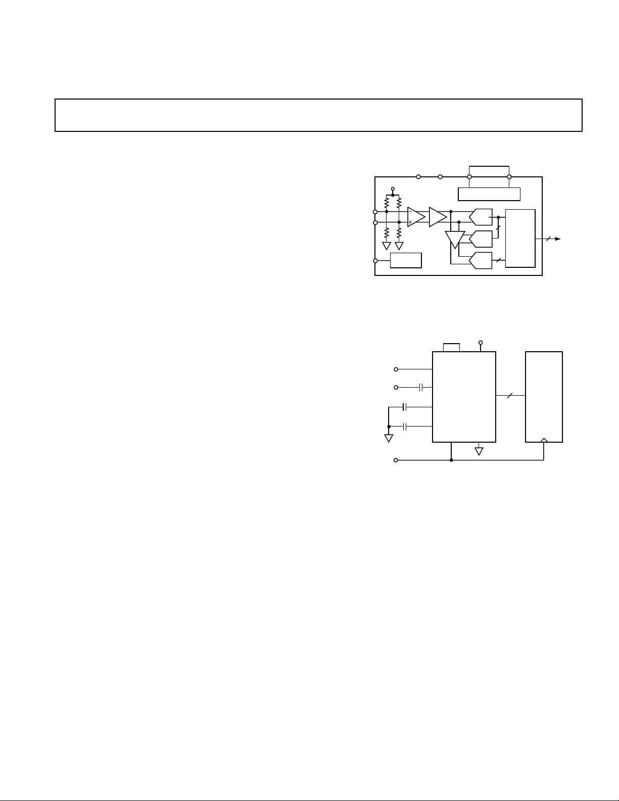
FUNCTIONAL BLOCK DIAGRAM
AINB
AIN
ENCODE
(+3.3V ± 0.512V)
ENCODE
GND
+5V
+5V
AD9049
T/H
TIMING
AIN
0.1µF
+5V
0.1µF
0.1µF
SUM
AMP
10
5
6
9
3
13
REFERENCE CKTS
ADC
DAC
ADC
+5V
2, 8, 11,
4
20, 22
AD9049
1, 7, 12,
21, 23
Figure 1. Typical Connections
DECODE
9 BITS
LOGIC
9
(2)
74AC574
REV. A
Information furnished by Analog Devices is believed to be accurate and
reliable. However, no responsibility is assumed by Analog Devices for its
use, nor for any infringements of patents or other rights of third parties
which may result from its use. No license is granted by implication or
otherwise under any patent or patent rights of Analog Devices.
One Technology Way, P.O. Box 9106, Norwood, MA 02062-9106, U.S.A.
Tel: 617/329-4700 World Wide Web Site: http://www.analog.com
Fax: 617/326-8703 © Analog Devices, Inc., 1996
Page 2

AD9049–SPECIFICATIONS
ELECTRICAL CHARACTERISTICS
(VD, VDD = +5 V; internal reference; ENCODE = 30 MSPS unless otherwise noted)
Test AD9049BR/BRS
Parameter Temp Level Min Typ Max Units
RESOLUTION 9 Bits
DC ACCURACY
Differential Nonlinearity +25°C I 0.5 1.0 LSB
Full V 0.5 LSB
Integral Nonlinearity +25°C I 0.5 1.0 LSB
Full V 0.5 LSB
No Missing Codes Full IV GUARANTEED
Gain Error +25°CI ±1.0 ±7.5 % FS
Gain Tempco
1
Full V ±100 ppm/°C
ANALOG INPUT
Input Voltage Range +25°C V 1.024 V p-p
Input Offset Voltage +25°C I –10 +7 +25 mV
Full IV –32 +51 mV
Input Resistance +25°C I 3.5 5.0 6.5 kΩ
Input Capacitance +25°CV 5 pF
Analog Bandwidth +25°C V 100 MHz
BANDGAP REFERENCE
Output Voltage +25°C I 2.4 2.5 2.6 V
Temperature Coefficient
1
Full V ± 50 ppm/°C
SWITCHING PERFORMANCE
Maximum Conversion Rate +25°C I 30 MSPS
Minimum Conversion Rate +25°C IV 1.5 3 MSPS
Aperture Delay (t
Aperture Uncertainty (Jitter) +25°C V 5 ps, rms
Output Propagation Delay (tPD)
) +25°C V 2.7 ns
A
2
Full IV 5 15 ns
DYNAMIC PERFORMANCE
Transient Response +25°CV 10 ns
Overvoltage Recovery Time +25°CV 10 ns
ENOBS
f
= 2.3 MHz +25°C V 8.56 ENOBs
IN
f
= 10.3 MHz +25°C I 8.01 8.51 ENOBs
IN
Signal-to-Noise Ratio (SINAD)
f
= 2.3 MHz +25°C V 53.3 dB
IN
f
= 10.3 MHz +25°C I 50 53 dB
IN
3
Signal-to-Noise Ratio
(Without Harmonics)
f
= 2.3 MHz +25°C V 53.5 dB
IN
f
= 10.3 MHz +25°C I 51 53.3 dB
IN
2nd Harmonic Distortion
f
= 2.3 MHz +25°C V –69 dBc
IN
f
= 10.3 MHz +25°C I –67 –60 dBc
IN
3rd Harmonic Distortion
f
= 2.3 MHz +25°C V –75 dBc
IN
f
= 10.3 MHz +25°C I –66 –58 dBc
IN
Two-Tone Intermodulation
Distortion (IMD)
4
+25°C V 65 dBc
Differential Phase +25°C V 0.15 Degrees
Differential Gain +25°C V 0.35 %
–2–
REV. A
Page 3

AD9049
Test AD9049BR/BRS
Parameter Temp Level Min Typ Max Units
ENCODE INPUT
Logic “1” Voltage Full IV 2.0 V
Logic “0” Voltage Full IV 0.8 V
Logic “1” Current Full IV 1 µA
Logic “0” Current Full IV 1 µA
Input Capacitance +25°C V 10 pF
Encode Pulse Width High (t
Encode Pulse Width Low (t
DIGITAL OUTPUTS
Logic “1” Voltage Full IV 4.95 V
Logic “0” Voltage Full IV 0.05 V
Logic “1” Voltage (3.0 V
Logic “0” Voltage (3.0 V
Output Coding Offset Binary Code
) +25°C IV 10 166 ns
EH
) +25°C IV 10 166 ns
EL
) Full IV 2.95 V
DD
) Full IV 0.05 V
DD
POWER SUPPLY
V
, VDD Supply Current
D
Power Dissipation
Power Supply Rejection Ratio
(PSRR)
NOTES
1
“Gain Tempco” is for converter only; “Temperature Coefficient” is for bandgap reference only.
2
Output propagation delay (tPD) is measured from the 50% point of the rising edge of the encode command to the midpoint of the digital outputs with 10 pF
maximum loads.
3
RMS signal to rms noise with analog input signal 0.5 dB below full scale at specified frequency.
4
Intermodulation measured relative to either tone with analog input frequencies of 9.5 MHz and 9.9 MHz at 7 dB below full scale.
5
Power dissipation is measured at 30 MSPS with AIN of 10.3 MHz and digital outputs loaded with 10 pF maximum. See Figure 4 for power dissipation at other
conditions.
6
Measured as the ratio of the change in offset voltage for 5% change in +VD.
Specifications subject to change without notice.
6
EXPLANATION OF TEST LEVELS
Test Level
I – 100% Production Tested.
IV – Parameter is guaranteed by design and characteriza-
tion testing.
V – Parameter is a typical value only.
5
5
Full IV 40 60 80 mA
Full IV 300 400 mW
+25°CI ±10 mV/V
ABSOLUTE MAXIMUM RATINGS*
VD, VDD . . . . . . . . . . . . . . . . . . . . . . . . . . . . . . . . . . . . . .+7 V
ANALOG IN . . . . . . . . . . . . . . . . . . . . . . –1.0 V to V
Digital Inputs . . . . . . . . . . . . . . . . . . . . . . . . . . . . –0.5 V to V
V
Input . . . . . . . . . . . . . . . . . . . . . . . . . . . . . . –0.5 V to V
REF
+ 1.0 V
D
D
D
Digital Output Current . . . . . . . . . . . . . . . . . . . . . . . . . 20 mA
Operating Temperature
AD9049BR/BRS . . . . . . . . . . . . . . . . . . . . . –40°C to +85°C
Storage Temperature . . . . . . . . . . . . . . . . . . . –65°C to +150°C
*Stresses above those listed under “Absolute Maximum Ratings” may cause
permanent damage to the device. This is a stress rating only and functional
operation of the device at these or any other conditions above those indicated in the
operational sections of this specification is not implied. Exposure to absolute
maximum ratings for extended periods may effect device reliability.
REV. A
ORDERING GUIDE
Model Temperature Range Package Option*
AD9049BR – 40°C to +85°C R-28
AD9049BRS –40°C to +85°C RS-28
*R = Small Outline (SO); RS = Shrink Small Outline (SSOP).
–3–
Page 4
AD9049
Table I. AD9049 Digital Coding (Single Ended Input AIN, AINB Bypassed to GND)
Digital Output
Analog Input Voltage Level MSB . . . LSB Digital Output
3.810 Positive Full Scale 111111111
3.300 Midscale 011111111
2.790 Negative Full Scale 000000000
PIN DESCRIPTIONS
Pin No Name Function
1, 7, 12, 21, 23 GND Ground.
2, 8, 11 V
3 VREF
4 VREF
D
OUT
IN
5 COMP Internal compensation pin, 0.1 µF bypass connected here to V
6 REF
BP
9 AINB Complementary analog input pin (Analog input bar).
10 AIN Analog input pin.
13 ENCODE Encode clock input to ADC. Internal T/H is placed in hold mode (ADC is encoding)
14 NC Not internally connected.
15 D8 (MSB) Most significant bit of ADC output.
16–19 D7–D4 Digital output bits of ADC.
20, 22 V
DD
24–26 D3–D1 Digital output bits of ADC.
27 D0 (LSB) Least significant bit of ADC output.
28 NC Not internally connected.
Analog +5 V ± 5% power supply.
Internal bandgap voltage reference (nominally +2.5 V).
Input to reference amplifier. Voltage reference for ADC is connected here.
(+5 V).
D
External connection for (0.1 µF) reference bypass capacitor.
on rising edge of encode signal.
Digital output power supply (only used by digital outputs).
PIN CONNECTIONS
GND
1
V
2
D
VREF
3
OUT
VREF
4
IN
5
6
REF
BP
GND
AINB
GND
ENCODE
AD9049
7
TOP VIEW
8
V
(Not to Scale)
D
9
AIN D4
10
V
11
D
12
13
NC
14
NC = NO CONNECT
28
27
26
25
24
23
22
21
20
19
18
17
16
15
NC
D0 (LSB)
D1
D2
D3COMP
GND
V
DD
GND
V
DD
D5
D6
D7
D8 (MSB)
CAUTION
ESD (electrostatic discharge) sensitive device. Electrostatic charges as high as 4000 V readily
accumulate on the human body and test equipment and can discharge without detection.
Although the AD9049 features proprietary ESD protection circuitry, permanent damage may
occur on devices subjected to high energy electrostatic discharges. Therefore, proper ESD
precautions are recommended to avoid performance degradation or loss of functionality.
WARNING!
ESD SENSITIVE DEVICE
–4–
REV. A
Page 5

AIN
ENCODE
DIGITAL
OUTPUTS
N N + 1 N + 2 N + 3 N + 4 N + 5
t
A
tEHt
EL
t
PD
N – 5 N – 4 N – 3 N – 2 N – 1 N
Figure 2. Timing Diagram
t
APERTURE DELAY 2.7ns
A
t
PULSE WIDTH HIGH 10ns 166ns
EH
t
PULSE WIDTH LOW 10ns 166ns
EL
t
OUTPUT PROP DELAY 5.0ns 8.2ns 15.0ns
PD
MIN TYP MAX
AD9049
AINB (Pin 9)
AIN (Pin 10)
V
D
INPUT
8k
8k
16k
V
REF
16k
V
D
Output
BUFFER
VREF
OUT
(Pin 3)
VDD (Pins 20, 22)
+3V to +5V
Output Stage
VREF
IN
(Pin 4)
Reference Circuit
D0–D8
V
D
ENCODE
(Pin 13)
Encode InputAnalog Input
V
D
A
V
VREF
BF
(Pin 6)
Figure 3. Equivalent Circuits
REV. A
–5–
Page 6

AD9049–Typical Performance Curves
361
342
323
304
285
266
247
DISSIPATION – mW
228
209
190
171
0
AIN = 10.3 MHz
OUTPUTS @ 5V
OUTPUTS @ 3V
10 20 30
CLOCK RATE – MSPS
Figure 4. Power Dissipation vs. Clock Rate
80
74
HARMONIC DISTORTION
68
62
dB
SIGNAL-TO-NOISE
56
50
44
38
1 10 100
ANALOG INPUT FREQUENCY – MHz
ENCODE = 30 MSPS
58
57
56
55
54
53
(SINAD)
52
51
SIGNAL-TO-NOISE RATIO – dB
50
49
48
– 20
–40
0
ENCODE = 30 MSPS
A
= 10.3 MHz
IN
20 40 60 80
TEMPERATURE – °C
Figure 7. SNR vs. Temperature
0
ENCODE = 30 MSPS
–10
f1 IN = 9.5 MHz @ –7 dBFS
f2 IN = 9.9 MHz @ –7 dBFS
–20
2f1–f2 = –65.4 dBc
2f2–f1 = –65.0 dBc
–30
–40
–50
–60
dB
–70
–80
–90
–100
–110
–120
0152.5 5 7.5 10 12.5
FREQUENCY – MHz
90
Figure 5. SNR/Distortion vs. Frequency
60
58
56
54
(SINAD)
52
50
SIGNAL-TO-NOISE RATIO – dB
48
46
0
AIN = 10.3 MHz
5
10 15 20 25 30
CLOCK RATE – MSPS
Figure 6. SNR vs. Clock Rate
Figure 8. Two-Tone IMD
0.50
0.25
0.00
–0.25
DIFF GAIN – %
–0.50
–0.25
DIFF PHASE – Degrees
–0.50
123456
0.50
0.25
0.00
123456
Figure 9. Differential Gain/Differential Phase
–6–
REV. A
Page 7

AD9049
TEMPERATURE – °C
15.0
10.0
–40
–20
t
PD
–
ns
020406080
14.0
11.0
9.0
8.0
13.0
12.0
[1] - 5V DATA RISING EDGE
[2] - 5V DATA FALLING EDGE
[3] - 3V DATA RISING EDGE
[4] - 3V DATA FALLING EDGE
7.0
6.0
5.0
100
[3]
[1]
[4]
[2]
0
–10
–20
–30
–40
–50
–60
dB
–70
–80
–90
–100
–110
–120
0152.5 5 7.5 10 12.5
FREQUENCY – MHz
ENCODE = 30 MSPS
ANALOG IN = 2.3 MHz
SNR = 53.0 dB
SNR (W/O HAR) = 53.3 dB
2ND HARMONIC = 69.3 dB
3RD HARMONIC = 72.9 dB
Figure 10. FFT Plot 30 MSPS, 2.3 MHz
0
–10
–20
–30
–40
–50
–60
dB
–70
–80
–90
–100
–110
–120
0152.5 5 7.5 10 12.5
FREQUENCY – MHz
ENCODE = 30 MSPS
ANALOG IN = 4.3 MHz
SNR = 53.0 dB
SNR (W/O HAR) = 53.3 dB
2ND HARMONIC = 69.0 dB
3RD HARMONIC = 72.6 dB
55.0
54.5
54.0
53.5
53.0
(SINAD)
52.5
SIGNAL-TO-NOISE – dB
52.0
51.5
51.0
25 30
35 4540 50 55
DUTY CYCLE – %
Figure 13. SNR vs. Clock Pulse Width
1.0
0.5
0.0
–0.5
–1.0
–1.5
–2.0
ADC GAIN – dB
–2.5
–3.0
–3.5
–4.0
–4.5
1
10
ANALOG INPUT FREQUENCY – MHz
ENCODE = 30 MSPS
A
= 2.3 MHz
IN
60 65 70 75
ENCODE = 30 MSPS
100
1000
REV. A
Figure 11. FFT Plot 30 MSPS, 4.3 MHz
0
ENCODE = 30 MSPS
–10
ANALOG IN = 10.3 MHz
SNR = 52.7 dB
–20
SNR (W/O HAR) = 53.1 dB
2ND HARMONIC = 66.4 dB
–30
3RD HARMONIC = 70.5 dB
–40
–50
–60
dB
–70
–80
–90
–100
–110
–120
0152.5 5 7.5 10 12.5
Figure 12. FFT Plot 30 MSPS, 10.3 MHz
FREQUENCY – MHz
–7–
Figure 14. ADC Gain vs. A
Frequency
IN
Figure 15. tPD vs. Temperature 3 V/5 V
Page 8

+5V
AD8041
1kΩ
1kΩ
+5V
AD9049
9
10
+5V
1kΩ
AD820
V
IN
–0.5V to +0.5V
1kΩ
0.1µF
0.1µF
+5V
AD8011
1kΩ
1kΩ
+5V
9
10
–5V
V
IN
–0.5V to +0.5V
0.1µF
AD9049
T1-1T
50Ω
V
IN
–0.5V to +0.5V
1
2
3
4
AD830
+15V
–5V
710
9
0.1µF
+5V
AD9049
AD9049
THEORY OF OPERATION
Refer to the block diagram on the front page.
The AD9049 employs a subranging architecture with digital
error correction. This combination of design techniques ensures
true 9-bit accuracy at the digital outputs of the converter.
At the input, the analog signal is buffered by a high speed differential buffer and applied to a track-and-hold (T/H) that holds
the analog value which is present when the unit is strobed with
an ENCODE command. The conversion process begins on the
rising edge of this pulse. The two stage architecture completes a
coarse and then a fine conversion of the T/H output signal.
Error correction and decode logic correct and align data from
the two conversions and present the result as a 9-bit parallel
digital word. Output data are strobed on the rising edge of the
ENCODE command. The subranging architecture results in
five pipeline delays for the output data. Refer to the AD9049
Timing Diagram.
USING THE AD9049
3 V System
The digital input and outputs of the AD9049 can easily be
configured to directly interface to 3 V logic systems. The encode
input (Pin 13) is TTL compatible with a logic threshold of 1.5
V. This input is actually a CMOS stage (refer to Equivalent Encode Input Stage) with a TTL threshold, allowing operation
with TTL, CMOS and 3 V CMOS logic families. Using 3 V
CMOS logic allows the user to drive the encode directly without
the need to translate to +5 V. This saves the user power and
board space. As with all high speed data converters, the clock
signal must be clean and jitter free to prevent the degradation of
dynamic performance.
The AD9049 outputs can also directly interface to 3 V logic
systems. The digital outputs are standard CMOS stages (refer to
AD9049 Output Stage) with isolated supply pins (Pins 20, 22
V
). By varying the voltage on the VDD pins, the digital output
DD
levels vary respectively. By connecting Pins 20 and 22 to the
3 V logic supply, the AD9049 will supply 3 V output levels.
Care should be taken to filter and isolate the output supply of
the AD9049 as noise could be coupled into the ADC, limiting
performance.
Analog Input
The analog input of the AD9049 is a differential input buffer
(refer to AD9049 Equivalent Analog Input). The differential inputs are internally biased at +3.3 V, obviating the need for
external biasing. Excellent performance is achieved whether the
analog inputs are driven single-ended or differential. (For best
dynamic performance, impedances at AIN and AINB should
match.)
Figure 16 shows typical connections for the analog inputs when
using the AD9049 in a dc coupled system with single ended
signals. All components are powered from a single +5 V supply.
The AD820 is used to offset the ground referenced input signal
to the level required by the AD9049.
AC coupling of the analog inputs to the AD9049 is easily accomplished. Figure 17 shows capacitive coupling of a single ended
signal while Figure 18 shows transformer coupling differentially
into the AD9049.
–8–
Figure 16. Single Supply, Single Ended, DC Coupled
AD9049
1kΩ
V
IN
–0.5V to +0.5V
1kΩ
+5V
–5V
0.1µF
AD8011
0.1µF
+5V
10
AD9049
9
Figure 17. Single Ended, Capacitively Coupled AD9049
Figure 18. Differentially Driven AD9049 Using Transformer Coupling.
The AD830 provides a unique method of providing dc level shift
for the analog input. Using the AD830 allows a great deal of
flexibility for adjusting offset and gain. Figure 19 shows the
AD830 configured to drive the AD9049. The offset is provided
by the internal biasing of the AD9049 differential input (Pin 9).
For more information regarding the AD830, see the AD830
data sheet.
Figure 19. Level Shifting with the AD830
REV. A
Page 9

AD9049
Overdrive of the Analog Input
Special care was taken in the design of the analog input section
of the AD9049 to prevent damage and corruption of data when
the input is overdriven. The nominal input range is +2.788 V to
3.812 V (1.024 V p-p centered at 3.3 V). Out-of-range comparators detect when the analog input signal is out of this range
and shut the T/H off. The digital outputs are locked at their
maximum or minimum value (i.e., all “0” or all “1”). This precludes the digital outputs from changing to an invalid value
when the analog input is out of range.
When the analog input signal returns to the nominal range, the
out-of-range comparators switch the T/H back to the active
mode and the device recovers in approximately 10 ns.
The input is protected to one volt outside the power supply
rails. For nominal power (+5 V and ground), the analog input
will not be damaged with signals from +6.0 V to –1.0 V.
Timing
The performance of the AD9049 is very insensitive to the duty
cycle of the clock. Pulse width variations of as much as ±10%
will cause no degradation in performance (see Figure 13, SNR
vs. Clock Pulse Width).
The AD9049 provides latched data outputs, with five pipeline
delays. Data outputs are available one propagation delay (t
PD
)
after the rising edge of the encode command (refer to the
AD9049 Timing Diagram). The length of the output data lines
and loads placed on them should be minimized to reduce transients within the AD9049; these transients can detract from the
converter’s dynamic performance.
The minimum guaranteed conversion rate of the AD9049 is
3 MSPS. Below a nominal of 1.5 MSPS the internal T/H
switches to a track function only. This precludes the T/H from
drooping to the rail during the conversion process and minimizes saturation issues. At clock rates below 3 MSPS dynamic
performance degrades. The AD9049 will operate in burst mode
operation, but the user must flush the internal pipeline each
time the clock stops. This requires 5 clock pulses each time the
clock is restarted for the first valid data output (refer to Figure 2 Timing Diagram).
Power Dissipation
The power dissipation specification in the parameter table is
measured under the following conditions: encode is 30 MSPS,
analog input is –1 dBFS at 10.3 MHz, the digital outputs are
loaded with approximately 7 pF (10 pF maximum), and V
DD
is
5 V. These conditions intend to reflect actual usage of the device.
As shown in Figure 4, the actual power dissipation varies based
on these conditions. For instance, reducing the clock rate will
reduce power as expected for CMOS type devices. Also the
loading determines the power dissipated in the output stages.
From an ac standpoint, the capacitive loading will be the key
(refer to Equivalent Output Stage).
The analog input frequency and amplitude in conjunction with
the clock rate determine the switching rate of the output data
bits. Power dissipation increases as more data bits switch at
faster rates. For instance, if the input is a dc signal that is out of
range, no output bits will switch. This minimizes power in the
output stages but is not realistic from a usage standpoint.
The dissipation in the output stages can be minimized by interfacing the outputs to 3 V logic (refer to USING THE AD9049,
3 V System). The lower output swings minimize consumption.
Refer to Figure 4 for performance characteristics.
Voltage Reference
A stable and accurate +2.5 V voltage reference is built into the
AD9049 (Pin 3, V
Output). In normal operation the internal
REF
reference is used by strapping Pins 3 and 4 of the AD9049 together. The internal reference has 500 µA of extra drive current
that can be used for other circuits.
Some applications may require greater accuracy, improved temperature performance or adjustment of the gain of the AD9049,
which cannot be obtained by using the internal reference. For
these applications, an external +2.5 V reference can be used to
connect to Pin 4 of the AD9049. The VREF
requires 5 µA of
IN
drive current.
The input range can be adjusted by varying the reference volt-
age applied to the AD9049. No appreciable degradation in performance occurs when the reference is adjusted ± 5%. The
full-scale range of the ADC tracks reference voltage changes
linearly.
REV. A
–9–
Page 10

AD9049
Figure 20. Evaluation Board Top Layer
Figure 21. Evaluation Board Ground Layer
Figure 22. Evaluation Board Bottom Layer
–10–
REV. A
Page 11

AD9049
U3
74AC574R
9
C14
0.1µF
8D
8
7D
7
6D
6
5D
5
4D
4
3D
3
2D
2
1D
9
8D
8
7D
7
6D
6
5D
5
4D
4
3D
3
2D
2
1D
CK
11
U4
74AC574R
CK
11
C15
0.1µF
U1
AD9049R
R5
1k
3
OUT
Y1
SW41
C9
0.1µF
6
GND
+5V
C7
0.1µF
TP3
2
R2
2k
+5V
2
IN
IN
3
R1
50
+5V
12
13
U6:D
74AC00R
J1
U2
AD9631Q
OUT
4
5
4
J6
+
C5
10µF
6
U6:B
74AC00R
VCC
11
R4
J2
1k
R3
50
J7
C1
0.1µF
C2
0.1µF
C3
0.1µF
+5V
3
4
5
6
9
10
13
VREFOUT
VREFIN
COMP
REFBP
AINB
AIN
ENC
+5V
C10
0.1µF
U6:A
74AC00R
1
2
9
10
U6:C
74AC00R
D8/MSB
NC
+5V
+5V
E1
C12
0.1µF
15
16
D7
17
D6
18
D5
19
D4
24
D3
25
D2
26
D1
27
D0
20
22
TP2
+5V
3
8
C13
0.1µF
12
8Q
13
7Q
14
6Q
15
5Q
16
4Q
17
3Q
18
2Q
19
1Q
OE
1
12
8Q
13
7Q
14
6Q
15
5Q
16
4Q
17
3Q
18
2Q
19
1Q
OE
1
C16
C17
C22
0.1µF
0.1µF
0.1µF
C23
0.1µF
+5V
HDR20
20
19
18
17
16
15
14
13
12
11
10
9
8
7
6
5
4
3
2
1
C24
0.1µF
J3
J5
C6
10µF
+
C8
0.1µF
–5.2V
–5.2V
C20
0.1µF
Figure 23. Evaluation Board Schematic
REV. A
–11–
Page 12

AD9049
OUTLINE DIMENSIONS
Dimensions shown in inches and (mm).
28-Lead SOIC
(R-28)
0.7125 (18.10)
0.6969 (17.70)
29 15
141
0.2992 (7.60)
0.2914 (7.40)
0.4193 (10.65)
0.3937 (10.00)
C2104a–2–12/96
PIN 1
0.0118 (0.30)
0.0040 (0.10)
0.311 (7.9)
0.078 (1.98)
0.068 (1.73)
0.008 (0.203)
0.002 (0.050)
0.0500
(1.27)
BSC
28 15
0.301 (7.64)
PIN 1
0.0256
(0.65)
BSC
0.0192 (0.49)
0.0138 (0.35)
28-Lead SSOP
0.407 (10.34)
0.397 (10.08)
0.015 (0.38)
0.010 (0.25)
0.1043 (2.65)
0.0926 (2.35)
SEATING
PLANE
(RS-28)
141
0.07 (1.79)
0.066 (1.67)
SEATING
PLANE
0.0125 (0.32)
0.0091 (0.23)
0.212 (5.38)
0.205 (5.21)
0.009 (0.229)
0.005 (0.127)
0.0291 (0.74)
0.0098 (0.25)
8°
0°
8°
0°
x 45°
0.0500 (1.27)
0.0157 (0.40)
0.03 (0.762)
0.022 (0.558)
–12–
PRINTED IN U.S.A.
REV. A
 Loading...