

Page 1
High Speed
a
FEATURES
77 MSPS Encode Rate
Bipolar Input Range
Low Error Rate
Overflow Bit
MIL-STD-883 Compliant Versions Available
APPLICATIONS
QAM Telecommunications
Electronic Warfare (ECM, ECCM, ESM)
Radar Guidance Digitizers
GENERAL DESCRIPTION
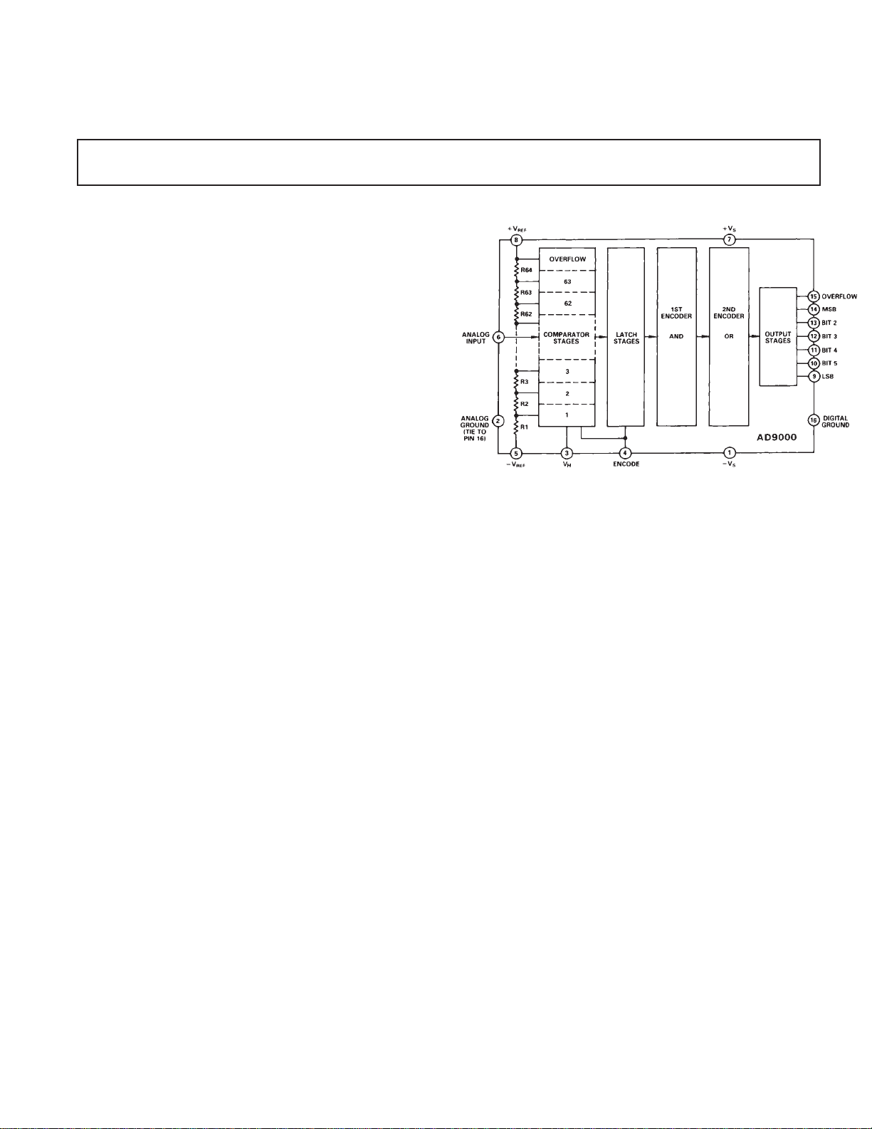
The AD9000 is a 6-bit, high speed, analog-to-digital converter
with ECL compatible outputs and a bipolar input stage. The
AD9000 is fabricated in a high performance bipolar process that
allows encode rates up to 77 MSPS.
The AD9000 employs the standard flash converter architecture
based on 64 individual comparators which simultaneously
determine the precise analog signal level. The comparators are
followed by two stages of decoding logic, allowing the AD9000
to operate with a very low error rate. The low 35 pF input
capacitance of the AD9000 greatly simplifies the analog driver
stage. An overflow output bit is also incorporated into the
AD9000 design as is a hysteresis control pin to modify comparator sensitivity.
6-Bit A/D Converter
AD9000
FUNCTIONAL BLOCK DIAGRAM
The AD9000 is offered as both a commercial temperature range
device, 0°C to +70°C, and as an extended temperature range
device, –55°C to +125°C. Both versions are available packaged
in a 16-pin ceramic DIP. The extended temperature range
device is also available in a 28-pin ceramic LCC package. The
extended temperature range versions are offered as fully compliant MIL-STD-883 Class B devices.
REV. A
Information furnished by Analog Devices is believed to be accurate and
reliable. However, no responsibility is assumed by Analog Devices for its
use, nor for any infringements of patents or other rights of third parties
which may result from its use. No license is granted by implication or
otherwise under any patent or patent rights of Analog Devices.
One Technology Way, P.O. Box 9106, Norwood, MA 02062-9106, U.S.A.
Tel: 617/329-4700 World Wide Web Site: http://www.analog.com
Fax: 617/326-8703 © Analog Devices, Inc., 1997
Page 2

AD9000–SPECIFICATIONS
(Supply Voltages = –5.2 V and +5.0 V; Differential Reference Voltage = 2.0 V
ELECTRICAL CHARACTERISTICS
Parameter Temp Min Typ Max Min Typ Max Units
RESOLUTION 6 6 Bits
DC ACCURACY
Differential Linearity +25°C 0.25 0.5 0.25 0.5 LSB
Integral Linearity +25°C 0.25 0.5 0.25 0.5 LSB
No Missing Codes Full GUARANTEED GUARANTEED
INITIAL OFFSET ERROR
Top of Reference Ladder +25°C 0.3 7/8 0.3 7/8 LSB
Bottom of Reference Ladder +25°C 0.25 7/8 0.25 7/8 LSB
Offset Drift Coefficient Full 145 145 µV/°C
ANALOG INPUT
Input Voltage Range Full ±2.0 V ±2.0 V V
Input Bias Current (Sampling)
Input Bias Current (Latched)
Input Resistance +25°C 3.0 3.0 kΩ
Input Capacitance +25°C3550 3550pF
Full Power Bandwidth
REFERENCE INPUT
2
3, 4
Reference Ladder Resistance +25°C 80 200 80 200 Ω
Ladder Temperature Coefficient 0.275 0.275 Ω/°C
Reference Input Bandwidth +25°C 20 20 MHz
DYNAMIC PERFORMANCE
Conversion Rate +25°C5070 7577 MHz
Conversion Time (+ 1 Clock) +25°C 20 13.3 ns
Aperture Delay (t
) +25°C2 2 ns
D
Aperture Uncertainty (Jitter) +25°C25 25 ps
Output Propagation Delay (t
Output Hold Time (t
Transient Response
Overvoltage Recovery Time
Output Rise Time
Output Fall Time
OH
8
10
10
Output Time Skew +25°C 0.4 0.4 ns
1
1
5
6
)
PD
7
)
9
unless otherwise noted)
Commercial Military
08C to +708C –558C to +1258C
AD9000JD AD9000SD/SE
Full 1.0 1.0 LSB
Full 1.0 1.0 LSB
Full 1.5 1.5 LSB
Full 1.5 1.5 LSB
Full 800 800 µA
Full 20 20 µA
+25°C 20 20 MHz
+25°C8 12 8 12 ns
+25°C8 14 8 14 ns
+25°C13 13 ns
+25°C11 11 ns
+25°C 5.0 4.5 ns
+25°C 5.0 4.5 ns
ENCODE INPUT
Logic “l” Voltage Full –1.1 –1.1 V
Logic “0” Voltage Full –1.5 –1.5 V
Logic “1” Current Full 100 100 µA
Logic “0” Current Full 100 100 µA
Input Capacitance +25°C 2.5 5.0 2.5 5.0 pF
ENCODE Pulse Width High (t
ENCODE Pulse Width Low (t
) +25°C 6.6 6.6 ns
PWH
) +25°C 6.6 6.6 ns
PWL
–2–
REV. A
Page 3

AD9000
ELECTRICAL CHARACTERISTICS
(Continued)
Commercial Military
08C to +708C –558C to +1258C
AD9000JD AD9000SD/SE
Parameter Temp Min Typ Max Min Typ Max Units
AC LINEARITY
Dynamic Linearity
11
12
+25°C 0.5 0.5 LSB
In-Band Harmonics
(DC to l MHz) +25°C 44 44 dBc
(l MHz to 5 MHz) +25°C 42 42 dBc
(5 MHz to 8 MHz) +25°C 38 38 dBc
Signal-to-Noise Ratio
Signal-to-Noise Ratio
Two Tone Intermodulation Rejection
Noise Power Ratio (NPR)
DIGITAL OUTPUTS
13
14
16
5
+25°C3133 3133 dB
+25°C4042 4042 dB
15
+25°C 46 46 dBc
+25°C 30 30 dBc
Logic “l” Voltage Full –1.1 –1.1 V
Logic “0” Voltage Full –1 .5 –1.5 V
POWER SUPPLY
17
Positive Supply Current (+5.0 V) +25°C6070 6070mA
Full 75 75 mA
Negative Supply Current (–5.2 V) +25°C6880 6880mA
Full 85 85 mA
Nominal Power Dissipation +25°C 675 675 mW
Reference Ladder Dissipation +25°C20 20 mW
NOTES
1
AIN = +V
2
Determined by 3 dB reduction in reconstructed output at 75 MSPS.
3
Under normal operating conditions, the analog input voltages should not
exceed nominal ±2 V operating range, nor the supply voltages (+VS and –VS),
whichever is smaller.
4
Under normal operating conditions the differential reference voltage may
range from ±0.5 V to ±2 V; +V
5
Output terminated with 100 Ω resistors to –2.0 V.
6
Measured from the leading edge of ENCODE to data out on Bit 1 (MSB).
7
Measured from the trailing edge of ENCODE to data out on Bit 1 (MSB).
8
For full-scale step input, 6-bit accuracy is attained in specified time.
ABSOLUTE MAXIMUM RATINGS
REF
.
≥ –V
REF
.
1
REF
Positive Supply Voltage . . . . . . . . . . . . . . . . . . . 0.3 V to +6 V
Negative Supply Voltage . . . . . . . . . . . . . . . . . 6.0 V to +0.3 V
Analog-to-Digital Ground Voltage Differential . . . . . . . . . 0.5
Analog Input Voltages (A
Differential Reference Voltage (+V
ENCODE Input Voltage . . . . . . . . . . . . . . . . . . . . – V
IN
, +V
REF
, –V
)2 . . . . . . . . . . +3 V
REF
REF
to –V
)3 . . . . . . . 6 V
REF
to 0 V
S
HYSTERESIS Control Voltage . . . . . . . . . . . . 0 V to + 3.0 V
Digital Output Current . . . . . . . . . . . . . . . . . . . . . . . . 20 mA
Power Dissipation (+25°C Free Air)
4
. . . . . . . . . . . . 745 mW
Operating Temperature Range
AD9000JD . . . . . . . . . . . . . . . . . . . . . . . . . . . . 0°C to +70°C
9
Recovers to 6-bit accuracy in specified time, after 150% full-scale input
overvoltage.
10
Measured on Bit 1 (MSB) only.
11
Measured at 50 MSPS encode rate.
12
Analog input frequency = 15 MHz.
13
RMS signal to RMS noise, with 540 kHz analog input signal.
14
Peak-to-peak signal to rms noise, with 540 kHz analog input signal.
15
f1 = 9.3 MHz, f2 = 7.6 MHz; Encode = 42 MHz.
16
DC to 8.2 MHz noise bandwidth with 3.886 MHz slot.
17
Supply voltage should remain stable within ±5% for normal operation.
Specifications subject to change without notice.
NOTES
1
Absolute maximum ratings are limiting values, to be applied individually, and
beyond which serviceability of the circuit may be impaired. Functional operability under any of these conditions is not necessarily implied. Exposure to
absolute maximum rating conditions for extended periods may affect device
reliability.
2
Under normal operating conditions, the analog input voltages should not
exceed nominal +2 V operating range, nor the supply voltages (+VS and –VS),
whichever is smaller.
3
Under normal operating conditions the differential reference voltage may range
from ±0.5 V to ±2 V; +V
4
Typical thermal impedances . . .
16-Pin Ceramic θJA = 67°C/W; θJC = 7°C/W
28-Pin LCC θJA = 62°C/W; θJC = 14°C/W
REF
≥ –V
REF.
AD9000SD/SE . . . . . . . . . . . . . . . . . . . . . . –55°C to +125°C
Storage Temperature Range . . . . . . . . . . . . –65°C to +150°C
Junction Temperature . . . . . . . . . . . . . . . . . . . . . . . . +175°C
Lead Soldering Temperature (10 sec) . . . . . . . . . . . . +300°C
REV. A
–3–
Page 4

AD9000
DIE LAYOUT
ORDERING GUIDE
1
Temperature Package
Device Range Description Option
AD9000JD 0°C to +70°C 16-Pin DIP, Industrial D-16
AD9000SD –55°C to +125°C 16-Pin DIP D-16
AD9000SE –55°C to +125°C 28-Pin LCC E-28A
NOTES
1
MIL-STD-883 versions available, contact factory.
2
D = Ceramic DIP; E = Leadless Ceramic Chip Carrier.
PIN DESIGNATIONS
2
MECHANICAL INFORMATION
Die Dimensions . . . . . . . . . . . . . . . . 129 × 217 × 15 (±2) mils
Pad Dimensions . . . . . . . . . . . . . . . . . . . . . . . . . . . . 4 × 4 mils
Metalization . . . . . . . . . . . . . . . . . . . . . . . 10,000Å Aluminum
Backing . . . . . . . . . . . . . . . . . . . . . . . . . . . . . . . . . . . . . None
Substrate Potential . . . . . . . . . . . . . . . . . . . . . . . . . . . . . . –V
S
Passivation . . . . . . . . . . . . . . . . . . . . . . . . 10,000Å Oxynitride
Die Attach . . . . . . . . . . . . . . . . . . . . . . . . . . . . . Gold Eutectic
Bond Wire . . . . . . . . 1.25 mil Aluminum; Ultrasonic Bonding
or 1 mil Gold; Gold Ball Bonding
PIN DESCRIPTIONS
Pin Name Description
–V
S
Negative supply terminal, nominally –5.2 V.
ANALOG GROUND Analog ground return. All grounds should be connected together near the AD9000.
V
H
The hysteresis control voltage varies the comparator hysteresis from 15 mV to 50 mV, for a change of 0 V
to +3 V at the hysteresis control pin.
ENCODE The ENCODE pin controls the conversion cycle. Encode is rising edge sensitive and should be driven
with a 50% duty-cycle waveform under normal conditions.
–V
A
+V
+V
REF
IN
S
REF
The most negative reference voltage for the internal resistor ladder.
Analog input pin.
Positive supply terminal, nominally +5.0 V.
Most positive reference voltage of the internal resistor ladder.
BIT 6 (LSB) One of six digital outputs. BIT 6 (LSB) is the least-significant-bit of the digital output.
BIT 5 – BIT 2 One of six digital outputs.
BIT 1 (MSB) One of six digital outputs. BIT 1 (MSB) is the most-significant-bit of the digital output.
OVERFLOW Overflow data output. Logic high indicates an input overvoltage (A
≥ +V
IN
REF
).
DIGITAL GROUND Digital ground return. All grounds should be connected together near the AD9000.
CAUTION
ESD (electrostatic discharge) sensitive device. Electrostatic charges as high as 4000 V readily
accumulate on the human body and test equipment and can discharge without detection.
Although the AD9000 features proprietary ESD protection circuitry, permanent damage may
occur on devices subjected to high energy electrostatic discharges. Therefore, proper ESD
precautions are recommended to avoid performance degradation or loss of functionality.
–4–
WARNING!
ESD SENSITIVE DEVICE
REV. A
Page 5

Figure 1. Functional Block Diagram
AD9000
Figure 2. System Timing Diagram
Figure 3. Burn-ln Test Circuit
REV. A
–5–
Page 6

AD9000
ABOUT THE AD9000
Analog Bandwidth
Quantifying the high frequency analog performance of the
AD9000 is somewhat difficult because of the various criteria
that can be applied. At one extreme there is the analog input
bandwidth of a single input comparator (which tends to be
extremely high). At the other end of the performance criteria is
the “no missing codes” restriction, which tends to be the most
conservative measure of analog bandwidth.
The “no missing codes” criteria simply means that the converter
is capable of generating all 64 output codes for an analog and
ENCODE frequency. At higher ENCODE rates to analog
frequencies, the converter continues to function, but with
reduced resolution. The graph below details the “no missing
codes” region of operation for the AD9000 at several reference
levels. Note that nearly all analog-to-digital converter applications operate in the oversampled region to avoid generation of
indeterminate data (aliasing).
Figure 4. Analog Input vs. Encode Rate “No Missing
Codes”
High-Speed Performance Enhancements
The AD9000 employs a hysteresis control pin which affects
comparator sensitivity. The error rate (number of full-scale
errors in a given period) is directly affected by the comparator
sensitivity. By varying the voltage on the hysteresis control pin,
the error rate can be reduced. The AD9000 is capable of extremely low error rate operation, which makes it ideal for error
sensitive applications such as QAM demodulation. If the
hysteresis control pin is used, it should be decoupled to
ground through a 0.1 µF capacitor, otherwise it may be left
floating.
At the highest encode rates, overall accuracy can be improved
by skewing the ENCODE signal duty-cycle to allow more time
in the “latch” mode. Specifically, extending the logic HIGH
portion of the ENCODE signal allows the comparators more
time to achieve an appropriate logic level prior to the decoding
cycle that begins on the rising edge of the ENCODE pulse.
Figure 5. Comparator Switching vs. Hysteresis Voltage
Layout Considerations
The AD9000, like all high-speed circuits, requires certain
precautions be taken to ensure optimum performance. The
foremost of these is the use of a substantial low impedance
ground plane around and under the AD9000. Just as important
are high quality ground connections to the AD9000 itself. It is
probably more effective to keep the analog and digital grounds
separate, except at the AD9000 where they should be connected
together. Sockets should generally be avoided due to the increased interlead capacitance they induce. If socketing must be
used, pin sockets are preferred.
Decoupling is especially important to high-speed analog circuits.
Each supply should be decoupled to ground with 0.1 µF ceramic
and 0.001 µF mica capacitors. The ladder reference pins should
be treated in a similar manner. In addition to decoupling the
reference ladder, the reference ladder should be driven from a
low output impedance source for the best noise rejection. In
all cases where practical, chip capacitors are recommended to
reduce the effects of lead inductance associated with standard
discrete capacitors.
MIL-STD-883 Compliance Information
The AD9000SE/SD/883C are classified within microcircuits
group 57-technology group D (bipolar A/D converters), and are
constructed in accordance with the latest revision of MIL-STD-
883. The AD9000 is electrostatic sensitive and falls within
electrostatic sensitivity classification Category A. PDA (Percent
Defective Allowance) is computed based on Subgroups 1 of the
specified Group A test list. QA screening is in accordance with
“Alternate Method A” of method 5005. The following apply:
Burn-In per 1015, Life Test per 1005, Electrical Testing per
5004. (Note: Group A electrical Testing assumes T
A = TC = TJ
.)
–6–
REV. A
Page 7

AD9000
TYPICAL APPLICATION
The AD9000 is a relatively flexible device that can be configured in a number of ways. One very useful feature of the
AD9000 is the open emitter outputs. The open emitters allow
the outputs of several AD9000s to be OR-wired in stacking
applications for increased resolution. This kind of application
depends on the return-to-zero nature of the output bits when
AIND≥ + V
(overflow). In circuits that employ only one
REF
AD9000, this is not always an advantage. The circuit below
illustrates one method of converting the outputs to nonreturnto-zero.
The 10197 (standard 10K ECL logic) hex-AND group senses
the active OVERFLOW output and forces all other bits to logic
HIGH. The 10151 latch is not required for AD9000 applications, but it may ease data transfer sensitivities in asynchronous
data collection systems.
The reference driver circuits should provide a low source impedance to prevent noise on the reference inputs from affecting
the AD9000’s accuracy. This is accomplished to a large extent
by adequately decoupling the reference pins to ground. An
improved method is employed below. The reference voltages
(+V
, –V
REF
) are buffered by a transistor/amplifier combina-
REF
tion. This has the advantages of wide bandwidth (hence low
impedance over a wide frequency range to eliminate high
frequency noise components), and improved temperature
stability.
REV. A
Figure 6.
–7–
Page 8

AD9000
AD9000/PCB EVALUATION AND TEST BOARD
Evaluating and testing the AD9000 is greatly simplified with the
AD9000/PCB evaluation board. The printed circuit board
contains all of the driver and buffering circuits needed to test
and evaluate the AD9000. The board outputs include both a
high quality reconstructed representation of the input waveform,
and a dc error waveform output that can be used to determine
device linearities.
Inputs to the AD9000/PCB evaluation board include the analog
signal to be digitized, as well as an optional ENCODE input for
high stability measurements. All components, except the AD9000,
are soldered onto the 8.5" × 6.3" board. The AD9000 is socketed to facilitate moderate volume testing. The evaluation board
is offered with either a commercial temperature range AD9000,
or an extended temperature range device installed.
The respective ordering numbers are AD9000JD/PCB and
AD9000SD/PCB.
C807a–21–8/87
16-Pin Ceramic
Figure 7. PCB Block Diagram
OUTLINE DIMENSIONS
Dimensions shown in inches and (mm).
–8–
28-Pin LCC
PRINTED IN U.S.A.
REV. A
 Loading...