

Page 1
8-Bit Octal, 4-Quadrant
V
IN
RR
V
OUT
V
OUT
= VIN • (D/128 – 1)
a
FEATURES
Low Cost
Replaces 8 Potentiometers
50 kHz 4-Quadrant Multiplying Bandwidth
Low Zero Output Error
Eight Individual Channels
3-Wire Serial Input
500 kHz Update Data Loading Rate
±3 V Output Swing
Midscale Preset, Zero Volts Out
APPLICATIONS
Automatic Adjustment
Trimmer Replacement
Vertical Deflection Amplitude Adjustment
Waveform Generation and Modulation
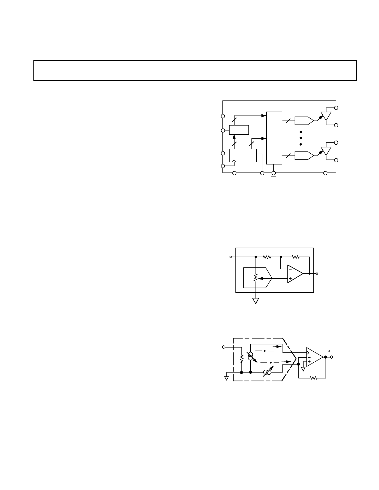
GENERAL DESCRIPTION
The AD8842 provides eight general purpose digitally controlled
voltage adjustment devices. The TrimDAC® capability allows
replacement of the mechanical trimmer function in new designs.
The AD8842 is ideal for ac or dc gain control of up to 50 kHz
bandwidth signals. The four-quadrant multiplying capability is
useful for signal inversion and modulation often found in video
vertical deflection circuitry.
Internally the AD8842 contains eight voltage output digital-toanalog converters, each with separate voltage inputs. A new
current conveyor amplifier design performs the four-quadrant
multiplying function with a single amplifier at the output of the
current steering digital-to-analog converter. This approach offers an improved constant input resistance performance versus
previous voltage switched DACs used in TrimDAC circuits,
eliminating the need for additional input buffer amplifiers.
Each DAC has its own DAC register that holds its output state.
These DAC registers are updated from an internal serial-toparallel shift register that is loaded from a standard 3-wire serial
input digital interface. Twelve data bits make up the data word
clocked into the serial input register. This data word is decoded
where the first 4 bits determine the address of the DAC register
to be loaded with the last 8 bits of data. A serial data output pin
at the opposite end of the serial register allows simple daisy
chaining in multiple DAC applications without additional external decoding logic.
Multiplying, CMOS TrimDAC
AD8842
FUNCTIONAL BLOCK DIAGRAM
DECODED
V
LD
SDI
CLK
DD
ADDRESS
8
LOGIC
4
SERIAL
REGISTER
GND
8
DATA
8 X 8
DAC
R
E
G
I
S
T
E
R
S
PRSDO
8
DAC A
AD8842
8
DAC H
The AD8842 consumes only 95 mW from ±5 V power supplies.
For single 5 V supply applications consult the DAC-8841. The
AD8842 is pin compatible with the 1 MHz multiplying bandwidth DAC8840. The AD8842 is available in 24-pin plastic
DIP and surface mount SOL-24 packages.
Figure 1. Functional Circuit of One 4-Quadrant
Multiplying Channel
CURRENT CONVEYOR
I1
I2
AMPLIFIER
= VIN (D/128–1)
R
V
IN
REF
R
256
D
(1- D)
256
V
IN
R
V
IN
R
VINA
G
V
A
OUT
VINH
G
V
H
OUT
V
SS
V
OUT
TrimDAC is a registered trademark of Analog Devices, Inc.
The current conveyor amplifier is a patented circuit belonging to Analog
Devices, Inc.
REV. 0
Information furnished by Analog Devices is believed to be accurate and
reliable. However, no responsibility is assumed by Analog Devices for its
use, nor for any infringements of patents or other rights of third parties
which may result from its use. No license is granted by implication or
otherwise under any patent or patent rights of Analog Devices.
Figure 2. Actual Current Conveyor Implementation of
Multiplying DAC Channel
One Technology Way, P.O. Box 9106, Norwood. MA 02062-9106, U.S.A.
Tel: 617/329-4700 Fax: 617/326-8703
Page 2
AD8842–SPECIFICATIONS
ELECTRICAL CHARACTERISTICS
(VDD = +5 V, V
= –5 V, All VINx = +3 V, TA = –40°C to +85°C, unless otherwise noted.)
SS
Parameter Symbol Conditions Min Typ Max Units
STATIC ACCURACY—All Specifications Apply for DACs A, B, C, D, E, F, G, H
Resolution N 8 Bits
Integral Nonlinearity Error INL ±0.2 ±1 LSB
Differential Nonlinearity DNL All Devices Monotonic ±0.4 ±1 LSB
Full-Scale Gain Error G
Output Offset V
Output Offset Drift TCV
VOLTAGE INPUTS—Applies to All Inputs V
Input Voltage Range
1
Input Resistance R
Input Capacitance C
DAC OUTPUTS—Applies to All Outputs V
Voltage Range
1
Output Current I
Capacitive Load C
DYNAMIC PERFORMANCE—Applies to All DACs
Full Power Gain Bandwidth
1
FSE
BZE
PR = 0, Sets D = 80
PR = 0, Sets D = 80
BZ
x
IN
IVR ±3 ±4V
IN
IN
x
OUT
OVR RL = 10 kΩ±3±4V
OUT
L
∆V
No Oscillation 500 pF
GBW VINx = ± 3 VP, RL = 2 kΩ, CL = 10 pF 10 50 kHz
H
H
12 19 kΩ
< 1.5 LSB ±3mA
OUT
2 LSB
525mV
5 µV/°C
9pF
Slew Rate Measured 10% to 90%
Positive SR+ ∆V
Negative SR– ∆V
Total Harmonic Distortion THD V
Spot Noise Voltage e
Output Settling Time t
Channel-to-Channel Crosstalk C
N
S
T
x = +5.5 V 0.5 1.0 V/µs
OUT
x = –5.5 V 1.0 1.8 V/µs
OUT
x = 4 V p-p, D = FFH, f = 1 kHz, 0.01 %
IN
= 80 kHz, RL = 1 kΩ
f
LPF
f = 1kHz, VIN = 0 V 78 nV/√Hz
±1 LSB Error Band, D = 00H to FF
D = FF
H
to 00
H
H
2.9 µs
5.4 µs
Measured Between Adjacent
Channels, f = 100 kHz 72 dB
Digital Feedthrough Q VINx = 0 V, D = 0 to 255
10
5 nV-s
POWER SUPPLIES
Positive Supply Current I
Negative Supply Current I
Power Dissipation
2
P
DD
SS
DISS
Power Supply Rejection PSRR
PR = 0 V 10 14 mA
PR = 0 V 9 13 mA
95 135 mW
PR = 0 V, ∆VDD = ±5% 0.0001 0.01 %/%
Power Supply Range PSR VDD, |VSS| 4.75 5.00 5.25 V
DIGITAL INPUTS
Logic High V
Logic Low V
Input Current I
Input Capacitance C
IH
IL
L
IL
2.4 V
7pF
Input Coding Offset Binary
DIGITAL OUTPUT
Logic High V
Logic Low V
TIMING SPECIFICATIONS
1
Input Clock Pulse Width tCH, t
Data Setup Time t
Data Hold Time t
CLK to SDO Propagation Delay t
DAC Register Load Pulse Width t
Preset Pulse Width t
Clock Edge to Load Time t
Load Edge to Next Clock Edge t
NOTES
1
Guaranteed by design, not subject to production test.
2
Calculated limit = 5 V × (IDD + ISS).
Specifications subject to change without notice.
DS
DH
PD
LD
PR
CKLD
LDCK
OH
OL
IOH = –0.4 mA 3.5 V
IOL = 1.6 mA 0.4 V
CL
60 ns
40 ns
20 ns
70 ns
50 ns
30 ns
60 ns
0.8 V
±10 µA
80 ns
REV. 0–2–
Page 3

1
SDI
0
1
CLK
0
1
LD
0
+3V
V
OUT
0V
DETAIL SERIAL DATA INPUT TIMING (PR = “1”)
1
SDI
(DATA IN)
(DATA OUT)
0
1
SDO
0
1
CLK
0
1
LD
0
+3V
V
OUT
0V
PRESET TIMING
1
PR
0
+3V
V
OUT
0V
A3 A2 A1 A0 D7 D6 D5 D4 D3 D2 D1 D0
t
CH
t
PR
t
S
±1 LSB ERROR BAND
t
CL
Ax or Dx
t
DS
t
DH
t
PD
t
CKLD
±1 LSB
t
LD
t
S
±1 LSB ERROR BAND
t
AD8842
DAC REGISTER LOAD
LDCK
±1 LSB
Figure 3. Timing Diagram
ABSOLUTE MAXIMUM RATINGS
(TA = +25°C unless otherwise noted)
VDD to GND . . . . . . . . . . . . . . . . . . . . . . . . . . . . –0.3 V, +7 V
V
to GND . . . . . . . . . . . . . . . . . . . . . . . . . . . . . +0.3 V, –7 V
SS
x to GND . . . . . . . . . . . . . . . . . . . . . . . . . . . . . . . VDD, V
V
IN
V
x to GND . . . . . . . . . . . . . . . . . . . . . . . . . . . . . VDD, V
OUT
Short Circuit I
x to GND . . . . . . . . . . . . . . . . . Continuous
OUT
Digital Input & Output Voltage to GND . . . . . . . . . . V
DD
SS
SS
, 0 V
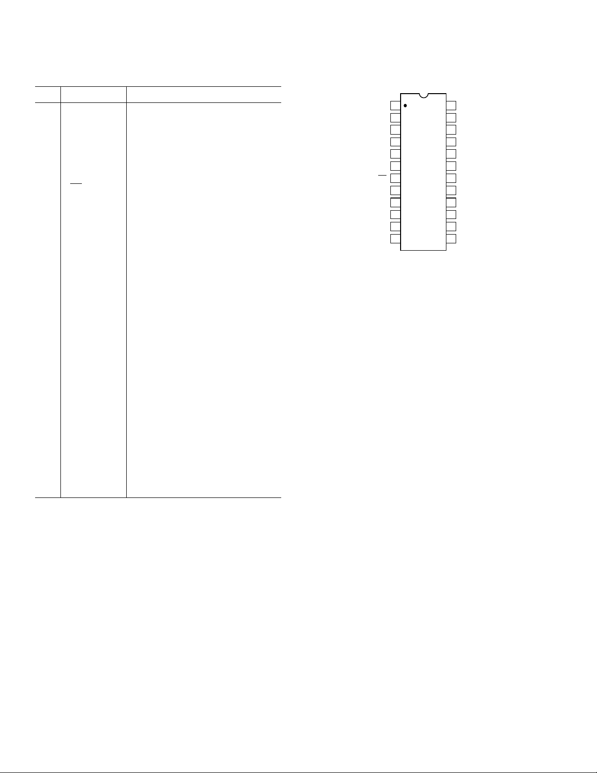
Model Range* Description Option
AD8842AN XIND 24-Pin 300mil P-DIP N-24
AD8842AR XIND 24-Pin 300mil SOIC SOL-24
*XIND = –40°C to +85°C. The AD8842 contains 2452 transistors.
ORDERING GUIDE
Temperature Package Package
Operating Temperature Range . . . . . . . . . . . . –40°C to +85°C
Maximum Junction Temperature (T
Max) . . . . . . . . . +150°C
J
Storage Temperature . . . . . . . . . . . . . . . . . . . –65°C to +150°C
Lead Temperature (Soldering, 10 sec) . . . . . . . . . . . . +300°C
Package Power Dissipation . . . . . . . . . . . . . . .(T
Thermal Resistance θ
JA,
Max–T
J
)/θ
A
JA
SOIC (SOL-24) . . . . . . . . . . . . . . . . . . . . . . . . . . . . 70°C/W
P-DIP (N-24) . . . . . . . . . . . . . . . . . . . . . . . . . . . . . 57°C/W
CAUTION
ESD (electrostatic discharge) sensitive device. Electrostatic charges as high as 4000 V readily
accumulate on the human body and test equipment and can discharge without detection.
Although the AD8842 features proprietary ESD protection circuitry, permanent damage may
occur on devices subjected to high energy electrostatic discharges. Therefore, proper ESD
precautions are recommended to avoid performance degradation or loss of functionality.
WARNING!
ESD SENSITIVE DEVICE
REV. 0 –3–
Page 4
AD8842
PIN DESCRIPTION
Pin Mnemonic Description
1V
2V
3V
4V
5V
C DAC C Output
OUT
B DAC B Output
OUT
A DAC A Output
OUT
B DAC B Reference Input
IN
A DAC A Reference Input
IN
6 GND Ground
7
8V
9V
10 V
11 V
12 V
13 V
14 V
15 V
PR Preset Input, active low, all DAC
registers = 80
E DAC E Reference Input
IN
F DAC F Reference Input
IN
E DAC E Output
OUT
F DAC F Output
OUT
G DAC G Output
OUT
H DAC H Output
OUT
G DAC G Reference Input
IN
H DAC H Reference Input
IN
H
16 LD Load DAC Register Strobe, active-
high input that transfers the data
bits from the serial-input register
into the decoded DAC register.
SDI and CLK inputs are disabled
when LD is high. See Tables I and II
17 CLK Serial Clock Input, positive edge
triggered
18 SDO Serial Data Output, active totem
pole output
19 V
SS
Negative 5 V Power Supply
20 SDI Serial Data Input
21 V
22 V
23 V
24 V
DD
D DAC D Reference Input
IN
C DAC C Reference Input
IN
D DAC D Output
OUT
Positive 5 V Power Supply
PIN CONFIGURATION
V
C
1
OUT
V
B
2
OUT
V
A
3
OUT
VINB
4
5
VINA
GND
PR
VINE CLK
VINF LD
V
OUT
V
OUT
V
OUT
AD8842
6
TOP VIEW
7
(Not to Scale)
817
916
E VINH
10 15
F VING
11
11
G VINH
12 13
24
23
22
21
20
19
18
14
V
OUT
VINC
VIND
V
DD
SDI
V
SS
SDO
D
REV. 0–4–
Page 5

LAST
LSB
D1 D2 D3 D4 D5 D6
D0
Table I. Serial Input Decode Table
FIRST
MSBD7LSB
A0
ADDRESSDATA
A1 A2
MSB LSB
MSB
A3
A3 A2 A1 A0
0
0
0
0
0
0
1
1
1
0
0
0
0
1
0
1
1
0
•
•
•
0
0
0
0
•
•
•
1
1
DAC UPDATED
NO OPERATION
0
DAC A
1
DAC B
0
DAC C
1
DAC D
0
DAC H
0
NO OPERATION
1
NO OPERATION
1
AD8842
MSB
D7 D6 D5 D4 D3 D2 D1 D0
0
0
0
0
0
0
0
0
1
1
1
1
1
1
0
0
0
0
1
1
1
1
0
0
0
•
•
•
1
1
0
0
0
0
•
•
•
1
1
1
1
LSB
DAC OUTPUT VOLTAGE
V
= (D/128 –1) x V
OUT
0
0
0
0
0
1
1
0
0
0
0
1
1
1
1
–V
IN
1
(1/128–1) x V
1
(127/128–1) x V
0
(128/128–1) x VIN = 0V; (PRESET VALUE)
1
(129/128–1) x V
0
(254/128–1) x V
1
(255/128–1) x VIN ≈ V
IN
IN
IN
IN
IN
IN
Table II. Input Logic Control Truth Table
CLK LD PR Input Shift Register Operation
L L H No Operation
↑ L H Shift One Bit in from SDI (Pin 20), Shift One Bit* Out from SDO (Pin 18)
X L L All DAC Registers = 80
H
X Η H Load Serial Register Data into DAC(X) Register
X H X Serial Data Input Register Loading Disabled
*Data shifted into the SDI pin appears twelve clocks later at the SDO pin.
REV. 0 –5–
Page 6

AD8842–Typical Performance Characteristics
–75 –50 –25 0
25 50 75 100 125
TEMPERATURE – °C
8
0
VINX = –3V
6
4
2
–2
–4
–8
–10
V
OUT
HALF SCALE – mV
VINX = +3V
VDD = +4.75V
VSS = –4.75V
3
2
–75 –50 –25
25
VDD = +4.75V
VSS = –4.75V
∆VIN = ±3V
1
0
4
0
50 75 100 125
TEMPERATURE – °C
SR+
SR–
V
OUT
– SLEW RATE – V/µs
1
0.4
0
10
100 100k10k1k
0.2
0.6
0.8
FREQUENCY – Hz
e
n
– NOISE VOLTAGE (µV/√Hz)
TA = +25°C
VIN = 0V
0.4
+1/2
+1/2
LINEARITY ERROR – LSB
–1/2
DACs A, B, C, D SUPERIMPOSED
0
–1/2
0
DACs E, F, G, H SUPERIMPOSED
DIGITAL INPUT CODE – Decimal
TA = +25°C
VDD = +5V
V
= – 5V
SS
VINX = +3V
2560 19212864
0.3
0.2
0.1
0
–0.1
–0.2
LINEARITY ERROR – LSB
–0.3
–0.4
TA = +125 °C
TA = –55 °C
DAC A
0 64 128
DIGITAL INPUT CODE – Decimal
TA = +25 °C
VDD = +5V
VSS = –5V
VINX = +3V
192 256
REFERENCE INPUT RESISTANCE – kΩ
–135
–180
PHASE – Degrees
–225
–270
–315
–360
Figure 4. Linearity Error vs.
Digital Code
21
VIN = +3V
20
19
18
17
16
–75 –50 100 125
AVG +2σ
AVG
AVG –2σ
VDD = +4.75V
VSS = –4.75V
–25 0 25 50 75
TEMPERATURE – °C
Figure 7. Input Resistance (V
vs. Temperature
GAIN
0
PHASE
–45
CODE = ALL ONES
–90
PHASE
CODE = ALL ZEROS
VIN = ± 100mV
TA = +25°C
10k 10M
100k 1M
FREQUENCY – Hz
Figure 10. Gain and Phase vs.
Frequency (Code = 00H or FFH)
–FS
+FS
Figure 5. Linearity Error vs.
Digital Code vs. Temperature
100
V
= +4Vp-p
IN
f
= 80kHz
LPF
10
CODE = FFH
1
0.1
0.01
TOTAL HARMONIC DISTORTION – %
0.001
10 100 1k 10k 100k
)
IN
0
–10
–20
–30
–40
Figure 8. Total Harmonic Distortion
vs. Frequency
INPUT A
0
OUTPUT B
15
30
GAIN – dB
45
60
75
90
CROSSTALK – dB
105
120
135
1k
RL = 2kΩ
FREQUENCY – Hz
dB
VINA = 100mV
VINB = 0V
TA = +25°C
10k 100k 1M 10M
FREQUENCY – Hz
pp
Figure 11. DAC Crosstalk
vs. Frequency
Figure 6. V
Half Scale (80H)
OUT
vs. Temperature
Figure 9. V
Slew Rate
OUT
vs. Temperature
Figure 12. Voltage Noise Density
vs. Frequency
REV. 0–6–
Page 7

AD8842
10
90
100
0%
2V
5µs
5V
10
90
100
0%
50ns
10mV
5µs
100
100
90
90
10
10
0%
0%
2V
2V
5µs
5µS
5µs
Figure 13. Pulse Response—Upper Trace V
Lower Trace V
100
100
90
90
10
10
0%
0%
OUT
5V
50mV
2V
@2 V/Div
5µs
5µs
500ns
5µS
@ 2 V/Div
IN
Figure 16. Settling Time—Upper Trace LD @ 5 V/Div,
Lower Trace V
@ 2 V/Div
OUT
Figure 14. Worst Case 1 LSB Step Change Code 80
Upper Trace LD @ 5 V/Div, Lower Trace V
5µs
5V
100
100
90
90
10
10
0%
0%
5mV
2V
Figure 15. Crosstalk—V
OUT
OUT
5µs
5µS
50ns
@ 5 mV/Div Figure 18. Clock Feedthrough—V
to 7FH,
H
@ 50 mV/Div
Figure 17. Digital Feedthrough—V
V
= 0 V; Code 7FH to 80
IN
100
90
10
0%
5mV
H
@ 10 mV/Div,
OUT
2µs
@ 5 mV/Div
OUT
REV. 0 –7–
Page 8

AD8842
40
30
20
10
0
100 1k 10k 100k 1M
FREQUENCY – Hz
POWER SUPPLY REJECTION – dB
+ PSRR
–PSRR
+ PSRR: VDD = +5V±250mV
–PSRR: VSS = –5V±250mV
5
4
1
3
2
0 100 300
0
–1
–6
6
200 400 500 600
T = HOURS OF OPERATION AT 150°C
HALF SCALE OFFSET – mV
–2
–3
–4
–5
χ
χ
– 2σ
χ
+ 2σ
VIN = +3V
2V
100
90
10
0%
2V
Figure 19. 10 kHz Sawtooth Waveform,
Upper Trace V
300
200
100
0
–100
–200
OUTPUT AMPLITUDE – mV
–300
–400
0
–3dB FREQUENCY
500 mVp-p INPUT AMPLITUDE
FREQUENCY – MHz
, Lower Trace V
IN
5
4321
20µs
Figure 20. AC Sweep Frequency 100 mV p-p Amplitude
OUT
12
11
10
SUPPLY CURRENT – mA
IDD @ VDD = +6V
AND V
IDD @ VDD = +4V
AND V
9
–ISS @ V
AND V
8
VINX = +3V
7
–75 –50 –25 0 25 50 75 100 125
Response
= –5V
SS
= –5V
SS
= +5V
DD
= –4V OR –6V
SS
TEMPERATURE – °C
80
60
40
20
0
–20
–40
OUTPUT AMPLITUDE – mV
–80
–100
0
–3dB FREQUENCY
100 mVp-p INPUT AMPLITUDE
FREQUENCY – MHz
5
4321
Figure 21. AC Sweep Frequency
500 mV p-p Amplitude Response
24
12
DATA = ØØ
0
–12
–24
GAIN – dB
–36
–48
–60
–72
1k 10M10k 1M100k
Figure 24. Gain (V
Feedthrough vs. Frequency
H
CØ
H
AØ
H
9Ø
H
88
H
84
H
82
H
81
H
80
H
FREQUENCY – Hz
OUT/VIN
VIN = 100mV
TA = +25°C
VDD = +5V
VSS = –5V
) and
AC
Figure 22. Supply Current vs.
Voltage and Temperature
TA = +25°C
15
VDD = +5V
VSS = –5V
10
CODE = 80
5
0
– mA
OUT
I
–5
–10
–15
–4 –3 –2 0–1 1 2 3 4
H
SHORT CIRCUIT
CURRENT
LIMITING
V
OUT
SHORT CIRCUIT
X – Volts
CURRENT
LIMITING
Figure 25. Short Circuit Limit
Output Current vs. Voltage
Figure 23. PSRR vs. Frequency
Figure 26. Output Voltage Drift
Accelerated by Burn-In
REV. 0–8–
Page 9

AD8842
CIRCUIT OPERATION
The AD8842 is a general purpose 8-channel ac or dc signallevel adjustment device designed to replace potentiometers used
in the three-terminal connection mode. Eight independent
channels of programmable signal level control are available in
this 24-pin package device. The outputs are completely buffered
providing up to 3 mA of output drive-current to drive external
loads. The functional equivalent DAC and amplifier combination shown in Figure 27 produces four-quadrant multiplication
of the signal inputs applied to V
times the digital input control
IN
word. In addition the AD8842 provides a 50 kHz full power
bandwidth in each four-quadrant multiplying channel. Operating from plus and minus 5 V power supplies, analog inputs and
outputs of ±3 V are easily accommodated.
V
IN
V
DAC
V
OUT
= 2 (D/256) × V
= (D/128 – 1) × V
AD8842 INPUT-OUTPUT VOLTAGE RANGE
4
RR
= D/256 × V
= 2 × V
DAC
IN
– V
IN
– V
IN
IN
IN
V
OUT
V
DAC
D = FFH
can be activated at any time to force the DAC registers to the
half-scale code 80
. This is generally the most convenient place
H
to start general purpose adjustment procedures.
Achieving 4-Quadrant Multiplying with a Current Conveyor
Amplifier
The traditional current output CMOS digital-to-analog converter requires two amplifiers to perform the current-to-voltage
translation and the half-scale offset to achieve four-quadrant
multiplying capability. The circuit shown in Figure 28 shows
one such traditional connection.
R/2
R/2
A1
R
A2
V
O
I
1
REF
V
IN
CURRENT OUT
DAC
GND
I
2
Figure 28. One Traditional Technique to Achieve FourQuadrant Multiplying with a Complementary Current
Output DAC
A single new current conveyor amplifier design emulates amplifiers A1 and A2 shown in Figure 28. Figure 29 shows the connection and equations that define this new circuit that achieves
four-quadrant multiplication with only one amplifier.
2
– Volts
0
OUT
V
–2
–4
–4 –2 0
V
= VIN (D/128 – 1), WHERE D = 0 TO 255
OUT
VIN – Volts
D = C0H
D = 80H
D = 40H
D = 00H
24
Figure 27. Functional Equivalent Circuit to the AD8842
Results in a 4-Quadrant Multiplying Channel
In order to simplify use with a controlling microprocessor a
PCB space saving three-wire serial data interface was chosen.
This interface can be easily adapted to almost all microcomputer and microprocessor systems. A clock (CLK), serial data
input (SDI) and a load (LD) strobe pins make up the three-wire
interface. The 12-bit input data word used to change the value
of the internal DAC registers contains a 4-bit address and 8-bits
of data. Using this word combination any DAC register can be
changed at a given time without disturbing the other channels.
A serial data output SDO pin simplifies cascading multiple
AD8842s without adding address decoder chips to the system.
During system power up a logic low on the preset
all DAC registers to 80
which in turn forces all the buffer am-
H
plifier outputs to zero volts. This asynchronous input pin
PR pin forces
PR
V
IN
REF
R
256
D
(1- D)
256
V
REF
R
V
REF
R
CURRENT CONVEYOR
AMPLIFIER
I
1
I
2
R
V
X
OUT
V
OUT
= VIN (D/128–1)
Figure 29. Current Conveyor Amplifier
Using the equations given in Figure 29 one can calculate the
final output equation as follows:
V
O
= –1–
=
=
D
256
D
256
2D
256
D
128
×
–1
–1
–1
V
IN
R
V
IN
V
IN
V
IN
× R –
+
256
–D
256
D
×V
V
IN
×
IN
× R
R
REV. 0 –9–
Page 10

AD8842
ADJUSTING AC OR DC SIGNAL LEVELS
The four-quadrant multiplication operation of the AD8842 is
shown in Figure 27. For dc operation the equation describing
the relationship between V
V
(D) = (D/128-1) × V
OUT
IN
, digital inputs and V
(1)
IN
OUT
is:
where D is a decimal number between 0 and 255
The actual output voltages generated with a fixed 3 V dc input
applied to V
are summarized in this table.
IN
Table III.
Decimal Comments
Input (D) V
(D) (VIN = 3 V)
OUT
0 –3.00 V Inverted FS
1 –2.98
127 –0.02
128 0.00 Zero Output
129 0.02
254 2.95
255 2.98 Full Scale (FS)
Notice that the output polarity is the same as the input polarity
when the DAC register is loaded with 255 (in binary = all ones).
Also note that the output does not exactly equal the input voltage. This is a result of the R-2R ladder DAC architecture chosen. When the DAC register is loaded with 0, the output
polarity is inverted and exactly equals the magnitude of the input voltage V
. The actual voltage measured when setting up a
IN
DAC in this example will vary within the ±1 LSB linearity error
specification of the AD8842. The calculated voltage error would
be ± 0.023 V (= ±3 V/128).
is an ac signal such as a sine wave, then we can use Equa-
If V
IN
tion 2 to describe circuit performance.
where
(t, D) = (D/128-1) × A sin (
V
OUT
ω
= 2 πf, A = sine wave amplitude, and D = decimal
ω
t) (2)
input code.
This transfer characteristic Equation 2 lends itself to amplitude
and phase control of the incoming signal V
. When the DAC is
IN
loaded with all zeros, the output sine wave is shifted by 180°
with respect to the input sine wave. This powerful multiplying
capability can be used for a wide variety of modulation, waveform adjustment and amplitude control.
SIGNAL INPUTS (VINA, B, C, D, E, F, G, H)
The eight independent VIN inputs have a constant inputresistance nominal value of 19 kΩ as specified in the electrical
characteristics table. These signal-inputs are designed to receive
not only dc, but ac input voltages. The signal-input voltage
range can operate to within one volt of either supply. That is,
the operating input-voltage-range is:
+ 1 V < VINx < (VDD – 1 V) (3)
V
SS
DAC OUTPUTS (V
A, B, C, D, E, F, G, H)
OUT
The eight D/A converter outputs are fully buffered by the
AD8842’s internal amplifier. This amplifier is designed to drive
up to 1 kΩ loads in parallel with 100 pF. However, in order to
minimize internal device power consumption, it is recommended whenever possible to use larger values of load resis-
tance. The amplifier output stage can handle shorts to GND;
however, care should be taken to avoid continuous short circuit
operation.
The low output impedance of the buffers minimizes crosstalk
between analog input channels. A graph (Figure 11) of analog
crosstalk between channels is provided in the typical performance characteristics section. At 100 kHz 70 dB of channel-tochannel isolation exists. It is recommended to use good circuit
layout practice such as guard traces between analog channels
and power supply bypass capacitors. A 0.01 µF ceramic in paral-
lel with a 1 µF–10 µF tantalum capacitor provides a good power
supply bypass for most frequencies encountered.
DIGITAL INTERFACING
The four digital input pins (CLK, SDI, LD, PR) of the AD8842
were designed for TTL and 5 V CMOS logic compatibility. The
SDO output pin offers good fanout in CMOS logic applications
and can easily drive several AD8842s.
The Logic Contro Input Truth Table II describes how to shift
data into the internal 12-bit serial input register. Note that the
CLK is a positive-edge sensitive input. If mechanical switches
are used for breadboard evaluation, they should be debounced
by a flipflop or other suitable means. The basic three-wire serial
data interface setup is shown in Figure 30.
ZERO VOLTAGE
OUTPUT PRESET
SERIAL DATA
CLOCK
LOAD STROBE
7
20
17
16
PR
AD8842
SDI
CLK
LD
21
+5V
6
19
–5V
Figure 30. Basic Three-Wire Serial Interface
The required address plus data input format is defined in the serial input decode Table I. Note there are 8 address states that
result in no operation (NOP) or activity in the AD8842 when
the positive edge triggered load-strobe (LD) is activated. This
NOP can be used in cascaded applications where only one DAC
out of several packages needs updating. The packages not requiring data changes would receive the NOP address, that is, all
zeros. It takes 12 clocks on the CLK pin to fully load the serialinput shift-register. Data on the SDI input pin is subject to the
timing diagram (Figure 3) data setup and data hold time requirements. After the twelfth clock pulse the processor needs to
activate the LD strobe to have the AD8842 decode the serialregister contents and update the target DAC register with the 8bit data word. This needs to be done before the thirteenth
positive clock edge. The timing requirements are provided in
the electrical characteristic table and in the Figure 3 timing diagram. After twelve clock edges, data initially loaded into the
shift register at SDI appears at the shift register output SDO. A
multiple package interface circuit is shown in Figure 31. In this
topology all the devices are clocked with the new data; however,
only the decoded package address signal updates the target
package LD strobe which is being used as a chip select.
REV. 0–10–
Page 11

AD8842
U
O
CLOCK
DATA
CODED
PACKAGE
ADDRESS
WR
ANALOG CONNECTIONS OMITTED FOR CLARITY
ADDRESSS
DECODE
EN
•
•
•
LD
CLK
SDI
LD
CLK
SDI
LD
CLK
SDI
AD8842
#1
AD8842
#2
•
•
•
AD8842
#N
Figure 31. Addressing Multiple AD8842 Packages
There is some digital feedthrough from the digital input pins.
Operating the clock only when the DAC registers require updating minimizes the effect of the digital feedthrough on the analog
signal channels. Measurements of DAC switch feedthrough
shown in the electrical characteristics table were accomplished
by grounding the V
x inputs and cycling the data codes be-
IN
tween all zeros and all ones. Under this condition 5 nV-s of
feedthrough was measured on the output of the switched DAC
channel. An adjacent channel measured less than 1 nV-s of digital crosstalk. The digital feedthrough and crosstalk photographs
shown in the typical performance characteristics section display
these characteristics (Figures 15 and 17).
Figure 32 shows a three-wire interface for a single AD8842 that
easily cascades for multiple packages. This circuit topology often
called daisy chaining requires preformating all the serial data for
each package in the chain. In the case of the 3 packages shown a
36 bit data word must be completely clocked into all the
AD8842 serial data input registers then the LD strobe would
transfer the data bits into the DAC registers updating one DAC
in each package.
µC
DATA
PA0
CLOCK
PA1
LD
PA2
SDI
CLK
LD
CLK
LD
CLK
LD
DAC A
AD8842 #1
SDO DAC H
DAC ASDI
AD8842 #2
SDO DAC H
DAC ASDI
AD8842 #3
SDO DAC H
V
O
•
•
•
V
•
•
Figure 32. Three-Wire Interface Updates Multiple
AD8842s
REV. 0 –11–
Page 12

AD8842
OUTLINE DIMENSIONS
Dimensions shown in inches and (mm).
24-Pin Narrow Body Plastic DIP Package
PIN 1
0.210
(5.33)
MAX
0.160 (4.06)
0.115 (2.92)
24
1
0.022 (0.558)
0.014 (0.356)
PIN 1
13
0.280 (7.11)
0.240 (6.10)
12
1.275 (32.30)
1.125 (28.60) 0.015
0.100 (2.54)
BSC
0.070 (1.77)
0.045 (1.15)
(0.38)
MIN
SEATING
PLANE
24-Pin Wide Body SOIC Package
24
1
0.6141 (15.60)
0.5985 (15.20)
13
12
0.2992 (7.60)
0.2914 (7.40)
0.1043 (2.65)
0.0926 (2.35)
0.130
(3.30)
MIN
0.4193 (10.65)
0.3937 (10.00)
0.325 (8.25)
0.300 (7.62)
0.0291 (0.74)
0.0098 (0.25)
0.195 (4.95)
0.115 (2.93)
0.015 (0.381)
0.008 (0.203)
C1904–18–4/94
x 45°
0.0118 (0.30)
0.0040 (0.10)
0.0500
(1.27)
BSC
0.0192 (0.49)
0.0138 (0.35)
0.0125 (0.32)
0.0091 (0.23)
0.0500 (1.27)
8°
0.0157 (0.40)
0°
PRINTED IN U.S.A.
REV. 0–12–
 Loading...